66
© 2010 by Maryam Sayyah. All rights reserved

© 2010 by Maryam Sayyah. All rights reserved

ELECTROCHEMICAL MULTIPHASE MICROSENSOR FOR DETECTION
OF ACETYLCHOLINESTERASE INHIBITORS
BY
MARYAM SAYYAH
THESIS
Submitted in partial fulfillment of the requirements
for the degree of Master of Science in Chemical Engineering
in the Graduate College of the
University of Illinois at Urbana-Champaign, 2010
Urbana, Illinois
Adviser:
Professor Richard I. Masel

ii
Abstract
In the present work, we utilize a microscale gas-liquid interface for use in a
selective gas microdetector for detection of toxic organophosphates (OP) compounds.
Previous work in our lab has demonstrated that OP compounds can be selectively
detected using such a sensor fabricated in polycarbonate; however, the sensor material is
not inert and cannot be integrated with other MEMS-based silicon devices. In this work
we focus on the design of a MEMS-based silicon sensor using both experiments and
COMSOL simulations. A Teflon nanoporous membrane is used to enhance the stability
of gas-liquid interface as well as sensitivity of detection. A toxic gas of interest is injected
into the vapor microchannel and reacts with an alkaline oxime solution as it dissolves in
the liquid phase. In the reaction cyanide ions are produced and detected using a gold
electrode on the nanoporous membrane. Response is measured as change in open circuit
potential between the working and reference electrodes integrated on a single chip. Due
to the toxicity of OP compounds, an OP simulant (e.g. acetic anhydride) which undergoes
a similar reaction mechanism has been used. The detection limit of this sensor design is
in the parts per trillion levels or approximately 3×10⁹ molecules.
In order to investigate the influences of important geometric parameters on
detector performance, a finite element based commercial software, COMSOL 3.4
(Stockholm, Sweden) has been utilized. A 2D simulation of the system consists of gas
and liquid microchannels with a nanoporous gas-liquid interface. Coupled steady state
Navier-Stokes, continuity and unsteady state mass transfer equations with chemical
reaction have been numerically solved to establish a realistic model of the system.
Simulation results indicate that using a nanoporous gas-liquid interface tremendously
reduces diffusion time of cyanide ions, leading to a fast response of the detector
compared to micron size membrane. Furthermore, it has been shown that the liquid
channel depth and nano-membrane porosity are amongst the main parameters affecting
the microsensor performance.
Experimental and simulation results demonstrate that the silicon based micro-
detector proposed in this work can be a promising way to selectively detect ultra low
levels of hazardous materials.

iii
Dedicated to my beloved father and mother

iv
Acknowledgments
I am heartily thankful to my advisor, Professor Richard I. Masel for his guidance
and support throughout this work. His insight and assistance throughout enabled me to
develop a thorough understanding of the subject.
I would also like to thank all of my colleagues in Professor Masel research group,
especially Kevin I. Lin, Dr. Amin Salehi-khojin, Dr. Chelsea N. Monty, Dr. Ilwhan Oh
and Nicolos Londono for helpful discussions. It was a great pleasure to having this
opportunity to work and share my thoughts with them.
I would also like to thank all the Mechanical Engineering cleanroom staff,
especially Mike Hansen and Glennys Mensing and also Dr. Junghoon Yeom, post-doc
associate in Professor Mark Shannon’s research group whose help and knowledge in
MEMS fabrication has guided me a lot in this project.
I owe my deepest gratitude to my family for their continued love and support.
They have always been a precious resource of encouragement in every aspect of my life.
This project would not have been possible without funding resource from Defense
Advanced Research Projects Agency (DARPA) under U.S. Air Force grant FA8650-04-
1-7121. Any opinions, findings, and conclusions or recommendations expressed in this
manuscript are those of the authors and do not necessarily reflect the views of the
Defense Advanced Projects Research Agency, or the U.S. Air Force.

v
Table of Contents
Chapter 1: Introduction ................................................................................................... 1
1.1 References ................................................................................................................. 2
Chapter 2: Literature review ........................................................................................... 4
2.1 Introduction ............................................................................................................... 4
2.2 Physical-based methods ............................................................................................ 5
2.2.1 Surface acoustic wave sensors ........................................................................... 5
2.2.2 Carbon nanotubes............................................................................................... 7
2.3 Chemical-based sensors .......................................................................................... 11
2.3.1 Overview of acetylcholinesterase enzyme ....................................................... 11
2.3.2 Chemical detection methods based on enzyme inhibition ............................... 13
2.4 Current methods limitations .................................................................................... 16
2.5 Oxime chemistry-based sensor ............................................................................... 17
2.6 Conclusion .............................................................................................................. 20
2.7 References ............................................................................................................... 21
Chapter 3: Statement of Purpose .................................................................................. 25
Chapter 4: Design and fabrication of the multiphase microdetector......................... 26
4.1 Introduction ............................................................................................................. 26
4.2 Mask design ............................................................................................................ 27
4.3 Microfabrication process sequence ......................................................................... 29
4.4 Sensor chip integration ........................................................................................... 31
4.5 Microreactor Simulation modeling with COMSOL 3.4 ......................................... 33
4.6 Conclusions ............................................................................................................. 36
4.7 References ............................................................................................................... 37
Chapter 5: Experimental testing of the fabricated microdetector ............................. 38
5.1 Introduction ............................................................................................................. 38
5.2 Materials and methods ............................................................................................ 38
5.2.1 Chemical preparation ....................................................................................... 38
5.2.2 Experimental set-up ......................................................................................... 39
5.3 Results and discussion ............................................................................................ 40
5.3.1 Experimental results......................................................................................... 40
5.3.2 Simulation results............................................................................................. 44
5.4 Conclusion .............................................................................................................. 49
5.5 References ............................................................................................................... 49
Chapter 6: Concluding remarks and future direction ................................................ 50
6.1 Concluding remarks ................................................................................................ 50
6.2 Future direction ....................................................................................................... 51
6.3 References ............................................................................................................... 54
Appendix A: Fabrication procedures............................................................................ 55
A.1 Sensor chip fabrication........................................................................................... 55
A.2 PDMS channel fabrication ..................................................................................... 56
Appendix B: Adhesive Transfer technique................................................................... 58
B.1 PDMS puck fabrication .......................................................................................... 58

vi
B.2 Recipe of bonding using adhesive .......................................................................... 58
B.3 D75 Adhesive recipe .............................................................................................. 58

1
Chapter 1
Introduction
Nowadays, there is a great need for an inexpensive, portable and fast sensor for
hazardous gas detection (chemical warfare agents, toxins, explosives). These sensors
should possess several characteristics1;
Vapor detection: the analyte of interest is in the gas phase
Sensitivity: the detection limit has to be in the order of part per billion (ppb) or
lower
Selectivity: it has to be highly reliable with the minimum false positives
Portability: the sensor should be light and easy to be carried by a person.
To achieve the criteria mentioned above, it is noticeable that the mechanism of
detection dictates the possibility to meet the first three points. Microfabrication
techniques can be employed to make a microsensor to be light enough to meet the
portability criteria. Over the last decade, microfabrication techniques are extensively used
in different aspects of chemistry and biology. Miniaturized analytical, sensing and
chemical synthesis in micro-total analytical systems (μTAS) and microreactors,
respectively represent the major extensions of microfabrication technology into chemical
and biological applications2-6
.
In addition to portability, sensors need to be selective and sensitive enough to be
able to detect the hazardous compounds before the human body can be affected. The
sensors based on specific chemistry/biochemistry show much higher selectivity toward
accurately recognizing target molecules from ambient air, which is particularly important
in the case of hazardous materials sensors.

2
Among different methods proposed in literature7-10
, electrochemical based
techniques can be a promising way for highly sensitive, selective and relatively simple
detection of OP molecules.
In this work, we report design and microfabrication of a novel electrochemical
microsensor which utilizes a composite gas-liquid interface for use in a selective
detection of toxic organophosphates (OP) compounds. Previous work in our lab11
has
demonstrated that OP compounds can be selectively detected using such a sensor
fabricated in polycarbonate; however, the sensor material is not inert and cannot be
integrated with other MEMS-based silicon devices. In this work we focus on the design
of a MEMS-based silicon sensor using both experiments and COMSOL simulations.
1.1 References
1. Oh, I.; Monty, C. N.; Masel, R. I., Electrochemical Multiphase Microreactor as
Fast, Selective, and Portable Chemical Sensor of Trace Toxic Vapors. Sensors
Journal, IEEE 2008, 8, (5), 522-526.
2. Jensen, K. F., Microreaction engineering- is small better? Chemcial Engineering
Science 2001, 56, 293-303.
3. Burns, M. A.; Johnson, B. N.; Brahmasandra, S. N.; Handique, K.; Webster, J. R.;
Krishnan, M.; Sammarco, T. S.; Man, P. M.; Jones, D.; Heldsinger, D.;
Mastrangelo, C. H.; Burke, D. T., An Integrated Nanoliter DNA Analysis Device
Science 1998, 282, 484 - 487.
4. Lagally, E. T.; Emrich, C. A.; Mathies, R. A., Fully integrated PCR-capillary
electrophoresis microsystem for DNA analysis. Lab Chip 2001, 1, 102-107.
5. Lagally, E. T.; Medintz, I.; Mathies, R. A., Single-Molecule DNA Amplification
and Analysis in an Integrated Microfluidic Device. Anal. Chem. 2001, 73, (3),
565-570.
6. Johnson, R. D.; Gavalas, V. G.; Daunert, S.; Bachas, L. G., Microfluidic ion-
sensing devices Analytica Chimica Acta 2008, 613, (1), 20-30.
3
7. Edward J. Staples; Viswanathan, S., Detection of Contrabands in Cargo
Containers Using a High-Speed Gas Chromatograph with Surface Acoustic Wave
Sensor. Industrial and Engineering Chemistry Research 2008, 47, (21), 8361-
8367.
8. Lee, C. Y.; Sharma, R.; Radadia, A. D.; Masel, R. I.; Strano, M. S., On-Chip
Micro Gas Chromatograph Enabled by a Noncovalently Functionalized Single-
Walled Carbon Nanotube Sensor Array. Angewandte Chemie-International
Edition, 2008, 47, (27), 5018-5021.
9. Lee, Y.; Choi, D.; Koh, W.-G.; Kim, B., Poly(ethylene glycol) hydrogel
microparticles containing enzyme-fluorophore conjugates for the detection of
organophosphorus compounds. Sensors and Actuators B: Chemical 2009, 137,
209-214.
10. Oh, I.; Masel, R. I., Electrochemical Organophosphate Sensor Based on Oxime
Chemistry. Electrochemical and Solid-State Letters 2007, 10, (2), J19-J22.
11. Oh, I.; Monty, C. N.; Masel, R. I., Electrochemical multiphase microreactor as
fast, selective, and portable chemical sensor of trace toxic vapors. . IEEE Sensors
Journal 2008, 8, (5), 522-526.
4
Chapter 2
Literature review
2.1 Introduction
Over the last decade, microfabrication is extensively used in different aspects of
chemistry and biology. Miniaturized analytical, sensing and chemical synthesis in micro-
total analytical systems (μTAS) and microreactors, respectively represent the major
extensions of microfabrication technology into chemical and biological applications1-5
.
Miniaturized analytical devices offer various advantages over traditional analytical
devices (e.g. ionization mobility spectrometry (IMS) and GC/MS) including smaller
sample consumption, enhanced sensitivity, shorter analysis time, low cost, and capability
of performing on-site analysis. These outstanding potentials can be used to develop high
sensitive and selective microsensors to detect trace toxic vapors such as
organophosphonate (OP) molecules (the case for this study).
Organophosphorus reagents which can be found in agricultural pesticides and
chemical warfare agents are extremely hazardous to human body as they inhibit primary
hydrolysis function of acetylcholinesterase enzyme (AChE). Hence, detection of
antiacetylcholinesterase agents is essential before the human body can be affected.
In this chapter, current methods for detection of organophosphorus pesticides,
advantages and disadvantages of each and lastly the proposed method of detection in this
work will be discussed.
In the laboratory setting, gas chromatography-mass spectroscopy (GC/MS) and
ion mobility spectroscopy (IMS) are two common ways of detection of gas phase
hazardous materials. High cost, low portability and high false positives (due to lack of
5
selectivity in IMS) make these methods not ideal for detection of ultra low level of
organophosphates.6 These methods need bulky and expensive instruments and also
require sampling and pre concentration and cannot be done in real time fashion. Besides,
there are strong demands for portable sensors to perform on-site analysis for a wide range
of oraganophosphates compounds in ambient air.
In this regard, some developed detection schemes are physical-based and some make
direct use of inhibition mechanism of acetylcholinesterase enzymes.
2.2 Physical-based methods
Two major categories of physical-based methods for detection of nerve agents are
surface acoustic waves7, 8
and carbon nanotubes9, 10
.
2.2.1 Surface acoustic wave sensors
Surface acoustic waves (SAW) sensors are a type of physical-based method of
detection which is extensively researched for the past decades. They have been used as
chemical vapor sensors. Upon molecules adsorption on a thin layer of sorbent, the mass
loading will change and causes changes in SAW characteristics such as amplitude, delay
and phase of the SAW device. To cancel out the environmental effect on the response the
identical uncoated SAW is used next to the working one which is exposed to the analyte
of interest11
. They operate in rf oscillation frequency ranges of a few MHz to GHz. By
properly choosing the sorbent, the response could be engineered toward recognizing a
particular analyte. Figure 2.1 shows the interaction of polymer coating with sarin in the
SAW device developed by McGill et al7.
6
Figure 2.1: Polymer coating interaction with sarin in SAW device. Adapted from reference7
In this device, an array of SAW devices each coated with specific polymer shows
a wide range of response to different analyte. Figure 2.2 illustrates the typical response of
SAW sensors to the mixture of water, DMMP (dimethyl methyl phosphate), Toluene and
bischloroether (CE). The combined response of each gives a specific response pattern
toward recognizing a particular analyte. To distinguish among different analytes, a
complex data analysis is necessary7.
Figure 2.2: Typical respone of SAW array sensors to mixture of water, DMMP,toluene and
bischloroether (CE). Adapted from reference 7
This method of detection is not very attractive for detection of specific chemicals. As
mentioned, this method is not selective. Moreover it is not so sensitive (in the order of
ppm).

7
2.2.2 Carbon nanotubes
Since carbon nanotubes possess especial characteristics such as high aspect ratio
(length to diameter) and their high fraction of surface atom, they seem ideal
nanomaterials to be incorporated into solid-state sensor technologies9. Molecular binding
events occurring at their interface can be electrically transduced as they form a
conduction channel between electrodes. They demonstrate a large change in resistance
when exposed to certain types of analytes. In such sensors, the adsorption of an analyte
molecule with strong electron donor or acceptor properties results in a partial charge
transfer between the analyte and the nanotube that changes its electrical resistance12
.
They are being extensively researched for use in environmental sensors (mainly
for detection of NH3, NO2, H2, CH4, CO, SO2, H2S), medical diagnostics (CO2, NO,
EtOH, organic vapors) and also for military and defense applications (CWAs and
explosives).
Novak et al.12
reported sub-ppb detection of DMMP, a stimulant of sarin by single
wall carbon nanotube (SWNT) based sensors. In this approach, they incorporated the
typical SWNT into the quartz flow cell and used Ag paint as contacts at the end (figure
2.3a). The resistance of this chemiresistor is between 1-10 MΩ. By this configuration
they were able to detect 1 ppb of DMMP (see figure 2.3 b).

8
a b
Figure 2.3: a) SWCNT flow-cell chemiresistor sensor made from 1/8 in. outer diameter quartz tubing b)
Response of the sensor to 1 ppb DMMP expressed as the relative change in resistance ∆R/R; adapted from
reference9
Strano et al.13
utilized the metallic nanotube FET devices with contact passivated
electrodes. By passivating the metal-nanotube contact, they could confirm the negligible
effect of metal-nanotube contact in signal transduction. In this study the response of the
sensors to SOCl2 and DMMP, simulants of nerve-agent precursors and sarin was
researched. Figure 2.4a shows a typical conductance change of nanotube sensor due to 3
mL of 100 ppm SOCl2 pulse for 10 sec. It clearly shows a partially irreversible response.
In order to have a reversible response, they injected water vapor onto the sensor set-up as
water hydrolyzes adsorbed SOCl2 and causes fast regeneration of the sensor.

9
Figure 2.4: a) Typical conductance change due to 3 mL of 100 ppm SOCl2 pulsed for 10 s. b) Rapid
regeneration of the sensor via adsorbed SOCl2 hydrolysis, adapted from reference13
One of the major problems associated with carbon nanotube sensor is that the
molecular adsorption is irreversible. Recently, carbon nanotube with specifically coated
polymers has been shown to engineer the sensor response and reversibility toward
detection of dimethyl methyl phosphonate (DMMP) vapor14
. In this study specific
polymer, polypyrrole, an amine with pKb~5.4 was used to functionalize carbon nanotube.
By doing that, sensitivity increased by three orders of magnitude while retaining
reversibility. Figure 2.5 shows the response of PPy functionalized SWNT to 1 ml DMMP
pulses.

10
Figure 2.5: a) Reversible conductance response from PPy-functionalized SWNT sensor upon exposure to 1-
mL DMMP pulses. b) DMMP response curve. Adapted from reference 14
Integration of miniaturized gas chromatography columns with various sensors
such as carbon nanotube14
, chemiresistive sensors15
or surface acoustic wave sensors8
based on non-specific bulk material properties such as resistivity change or frequency
change, respectively are amongst important non-selective detection schemes. The major
drawback of these methods lies in non-selective nature of detection. Although polymer
functionalization has improved sensitivity of the sensor response14
it still lacks selectivity
in detection. Polymer coated carbon nanotube or other chemiresistive methods show a
wide range of response to polar molecules as well as nonpolar ones16
. So the major
challenge is selectivity issues. To circumvent this problem and get the analyte specific
response, an array of sensor along with some data analysis is used. In this method,
multiple sensor elements each decorated with different sensing materials (e.g. polymers15
,
non-polymer sorbents15, 17
, metals18
) are used simultaneously. The combined response of
each gives a specific response pattern toward recognizing a particular analyte. Usually
11
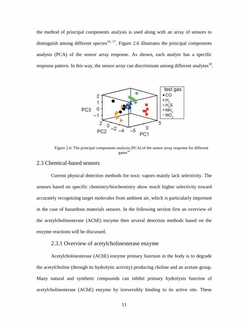
the method of principal components analysis is used along with an array of sensors to
distinguish among different species16, 17
. Figure 2.6 illustrates the principal components
analysis (PCA) of the sensor array response. As shown, each analyte has a specific
response pattern. In this way, the sensor array can discriminate among different analytes18
.
Figure 2.6: The principal components analysis (PCA) of the sensor array response for different
gases18
2.3 Chemical-based sensors
Current physical detection methods for toxic vapors mainly lack selectivity. The
sensors based on specific chemistry/biochemistry show much higher selectivity toward
accurately recognizing target molecules from ambient air, which is particularly important
in the case of hazardous materials sensors. In the following section first an overview of
the acetylcholinesterase (AChE) enzyme then several detection methods based on the
enzyme reactions will be discussed.
2.3.1 Overview of acetylcholinesterase enzyme
Acetylcholinesterase (AChE) enzyme primary function in the body is to degrade
the acetylcholine (through its hydrolytic activity) producing choline and an acetate group.
Many natural and synthetic compounds can inhibit primary hydrolysis function of
acetylcholinesterase (AChE) enzyme by irreversibly binding to its active site. These

12
compounds such as nerve gases particularly organophosphates (e.g. sarin) and
insecticides are called acetylcholinesterase inhibitors. Increased amount of acetylcholine
(Ach) in central and peripheral sites of nerve systems due to inhibition of AChE causes
convulsion and paralysis of the respiratory muscles19, 20
.
Figure 2.7 illustrates the three major domains of AChE enzyme: 1) the Esteratic
Locus with histidine and serine residues, 2) Anionic region with glutamic residue where
the quaternary ammonium pole of acetylcholine binds and 3) the hydrophobic regions
where it is important in binding aryl substrates21
.
Figure 2.7: Active sites of AChE enzyme21
Acetylcholinesterase inhibitors exert their biological effects on the enzyme by
irreversible binding to its active sites. Some of the inhibitors only bind to Esteratic
domain or Anionic regions. Some binds to both sites. Some compounds which have
quaternary structures such as decamethonium, tetraethylammonium,
tetrepropylammonium, and endrophonium bind to anionic region and inhibit the substrate
to attach. Majority of inhibitors only binds to esteratic sites and the phosphorylated
enzyme is hard to hydrolyze reversibly. Paraoxon, malathion, parathion, and ethion are
those organophosphates which only binds to esteratic site.

13
2.3.2 Chemical detection methods based on enzyme inhibition
In a recent study, Lee et al.22
developed an optical biosensor with hydrogel
microparticles containing enzyme-fluorophore conjugate which works based on the
inhibition of AChE activity by organophosporous compounds. Reaction between AChE
and acetylcholine chloride (AChCl) produces acetic acid which affects PH. In the
presence of AChE inhibitor, the concentration of AChCl is increased and it in turn
changes the emission density of AChE and SNAFL-1 mixture solution as emission peaks
of SNAFL-1 varies according to pH changes. SNAFL-1 is carboxy
seminaphthofluorescein, a pH-sensitive fluorophore, which has been utilized in this study.
Figure 2.8 illustrates the change in emission density as a function of AChCl.
Figure 2.8: The change in emission density as a function of acetylcholine chloride (AChCl).
This method involves synthesis and preparation of conjugated particles and use of
fluorescent spectrophotometer for detection. The detection scheme is so selective but the
reaction happens all in the liquid phase which imposes mass transfer limitation. Therefore,
14
this method cannot be used for fast detection of organophosporous compounds in the
ambient air.
In some other studies, in order to stabilize the AChE enzyme and thus increase the
sensor performances, its immobilization on various nanomaterial surfaces such as carbon
nanotubes23-26
, gold nanoparticles (AuNPs), etc.27-29
have been studied. By doing that,
electron transfer reactions happen at a lower overpotential due to their structure
dependent metallic character and their high surface area. They provide a ground for
unique biochemical sensing systems23
.
Liu et al.24
reported immobilization of AChE on negatively charged CNT by Layer by
layer assembly method via cationic poly (diallyldimethylammonium chloride) PDDA. As
illustrated in figure 2.9 unique sandwich-like structure (PDDA/AChE/PDDA) on the
CNT surface formed by self-assembling provides a favorable microenvironment to keep
the bioactivity of AChE24
.

15
Figure 2.9: Schematic of Layer by layer assembly of AChE on CNT via PDDA. A) Deposition of
PDDA, B) assembling negatively charged AChE C) deposition the second layer of PDDA. Adapted from
Reference 24
The reaction mechanism is illustrated in the equation below. Inhibition of AChE
by Paraoxon reduces the rate at which the reaction occurs as the available active sites are
blocked by paraoxon.
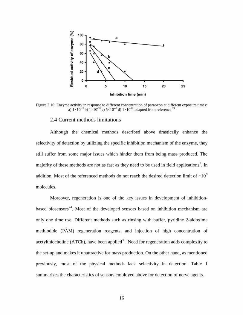
2acetylthiocholine H OAChE thiocholine acetate acid (1)
Incubation of biosensor by Paraoxon for certain duration causes decrease in
enzyme activity as shown in figure 2.10.
16
Figure 2.10: Enzyme activity in response to different concentration of paraoxon at different exposure times:
a) 1×10-12
b) 1×10⁻¹⁰
c) 5×10--9
d) 1×10⁻⁸
. adapted from reference 24
2.4 Current methods limitations
Although the chemical methods described above drastically enhance the
selectivity of detection by utilizing the specific inhibition mechanism of the enzyme, they
still suffer from some major issues which hinder them from being mass produced. The
majority of these methods are not as fast as they need to be used in field applications9. In
addition, Most of the referenced methods do not reach the desired detection limit of ~109
molecules.
Moreover, regeneration is one of the key issues in development of inhibition-
based biosensors24
. Most of the developed sensors based on inhibition mechanism are
only one time use. Different methods such as rinsing with buffer, pyridine 2-aldoxime
methiodide (PAM) regeneration reagents, and injection of high concentration of
acetylthiocholine (ATCh), have been applied30
. Need for regeneration adds complexity to
the set-up and makes it unattractive for mass production. On the other hand, as mentioned
previously, most of the physical methods lack selectivity in detection. Table 1
summarizes the characteristics of sensors employed above for detection of nerve agents.

17
Type Analyte Detection limit Response time Reversibility Reference
SWNTs DMMP <1 ppb 1000 sec Reversible
(3V gate bias)
Novak et al.12
SWNTs SOCl2, DMMP 100 ppm 10 sec Irreversible Lee et al. 13
Polymer-
coated SWNT
DMMP, DIMP 25-50 ppm 10 min Reversible
(vacuum)
Cattanach et
al.31
SAW DMMP ppm 50 sec Reversible McGill et al.7
CNT-enzyme Paraoxon 1×10-12
M min Reversible(regeneration
reagents)
Liu et al. 24
Table 1: Current sensor characteristics in detection of nerve agents
The issues of current methods hinder them to be used in field application. Speed,
simplicity, selectivity, sensitivity and ability to detect in gas phase are all important
aspects of a portable sensor.
2.5 Oxime chemistry-based sensor
Oxime compounds were found to mimic the active sites of AChE enzyme.
Therefore it could reactivate the phosphorylated enzyme. Oxime compounds are highly
reactive to organophosphates and restore the activity of the inhibited enzyme. In previous
work by Dr. Ilwhan Oh in our research group, 1-Phenyl-1,2,3,-butanetrione 2-oxime
(PBO) was used in order to hydrolyze toxic phosphonates in the beaker-scale32
. The
reaction of hydroxamic acids with organophosphorus antiacetylcholinesterase in neutral
or slightly alkaline aqueous solutions can be used as an effective way of detection.
Different oxime compounds such as 1-phenyl- 1,2,3-butanetrione 2-oxime (PBO),
1,3-diphenyl-1,2,3-propanetrione 2-oxime (DPO), anti-pyruvic aldehyde 1-oxime (PAO),
2-isonitrosoacetophenone (IAP) have been studied. PBO has been identified as the one

18
which shows a large and sharp response upon injection of acetic anhydride (AA), a
stimulant of organophosphates which undergoes the similar reaction mechanism (figure
2.11).
Figure 2.11: Electrode potential response of CN ISE in 25 mM borate buffer,(pH 10), 5 mM
solution of different oximes(1-phenyl- 1,2,3-butanetrione 2-oxime (PBO), 1,3-diphenyl-1,2,3-propanetrione
2-oxime (DPO), anti-pyruvic aldehyde 1-oxime (PAO), 2-isonitrosoacetophenone (IAP)). Adapted from
reference 32
Although no simple and generalized mechanism for the reaction between
hydroxamic acids (e.g. diketo-oxime) and organophosphorous was observed34
, it was
shown that it involves an overall rate limiting attack of an oxime anion on to the
phosphorus compound and formation of a complex intermediate (oxime phosphonate)
followed by a rapid split of oxime phosphonate into acidic products33
.
As illustrated in figure 2.1232
, hydrogen cyanide is one of the acidic products
from which the amount of phosphorous present in the sample can be obtained. The
production of cyanide ion in the reaction can be electrochemically detected by a potential
change from cyanide ion selective electrode (CN ISE)32
. More complex reaction
mechanism between oxime and antiacetylcholinesterase agents is described elsewhere34
.
In the figure 2.13, other pathways have also considered for the breakdown of
phosphorylOX to yield cyanide ion via benzoyl cyanide(step 2), reaction with more OX

19
to yield cyanide ion via both benzoyl cyanide and finally reaction with hydroxide ion to
yield OX and phosphorous acid(step 5).
Figure 2.12: Mechanism of the reaction between monoketo-oxime and organophosphate
compound.32

20
Figure 2.13: More rigorous reaction mechanism which accounts for the breakdown of
phosphorylOX in different pathways34
.
2.6 Conclusion
Current detection methods lack selectivity, sensitivity, speed and stability for long
term applications in field. The sensors based on specific chemistry/biochemistry show
much higher selectivity toward accurately recognizing target molecules from ambient air,
which is particularly important in the case of hazardous materials sensors. Among
different methods proposed in literature8, 14, 22
electrochemical based techniques can be a
promising way for highly sensitive, selective and relatively simple detection of OP
molecules. In this work, we aim to utilize the chemical reaction between hydroxamic
acids and analyte of interest, antiacetylcholinesterase which is well studied in our group32,
33. The reaction of hydroxamic acids with organophosphorus antiacetylcholinesterase in
neutral or slightly alkaline aqueous solutions can be used as an effective way of detection.

21
This thesis will highlight the development of oxime chemistry into a micro-scale
device as well as sensor optimization and integration. This scheme will present a
promising way for detection of hazardous chemicals in the gas phase which alleviates
most of the limitations associated with current physical and chemical methods.
2.7 References
1. Jensen, K. F., Microreaction engineering- is small better? Chemcial Engineering
Science 2001, 56, 293-303.
2. Burns, M. A.; Johnson, B. N.; Brahmasandra, S. N.; Handique, K.; Webster, J. R.;
Krishnan, M.; Sammarco, T. S.; Man, P. M.; Jones, D.; Heldsinger, D.;
Mastrangelo, C. H.; Burke, D. T., An Integrated Nanoliter DNA Analysis Device
Science 1998, 282, 484 - 487.
3. Lagally, E. T.; Emrich, C. A.; Mathies, R. A., Fully integrated PCR-capillary
electrophoresis microsystem for DNA analysis. Lab Chip 2001, 1, 102-107.
4. Lagally, E. T.; Medintz, I.; Mathies, R. A., Single-Molecule DNA Amplification
and Analysis in an Integrated Microfluidic Device. Anal. Chem. 2001, 73, (3),
565-570.
5. Johnson, R. D.; Gavalas, V. G.; Daunert, S.; Bachas, L. G., Microfluidic ion-
sensing devices Analytica Chimica Acta 2008, 613, (1), 20-30.
6. Sun, Y.; Ong, K. Y., Detection technologies for chemical warfare agents and
toxic vapors. CRC press: Boca Raton, FL, 2005.
7. McGill, R. A.; Nguyen, V. K.; Chung, R.; Shaffer, R. E.; DiLella, D.; Stepnowski,
J. L.; Mlsna, T. E.; Venezky, D. L.; Dominguez, D., The ‘‘NRL-SAWRHINO’’: a
nose for toxic gases. Sensors and Actuators B: Chemical 2000, 65, (10-13).
8. Edward J. Staples; Viswanathan, S., Detection of Contrabands in Cargo
Containers Using a High-Speed Gas Chromatograph with Surface Acoustic Wave
Sensor. Industrial and Engineering Chemistry Research 2008, 47, (21), 8361-8367.
9. Kauffman, D. R.; Star, A., Carbon Nanotube Gas and Vapor Sensors. Angewandte
Chemie 2008, 47, 6550 - 6570.
10. Ting Zhang; Mubeen, y.; Myung, N. V.; Deshusses, M. A., Recent progress in
carbon nanotube-based gas sensors. Nanotechnology 2008, 19.

22
11. Nimala, A. T.; Mittala, U.; Singha, M.; Khanejaa, M.; Kannanb, G. K.; J.C.
Kapoorb; Dubeyc, V.; Gutchc, P. K.; Lal, G.; Vyasc, K. D.; Gupta, D. C.,
Development of handheld SAWvapor sensors for explosives and CW agents.
Sensors and Actuators B: Chemical 2009, 135 399-410.
12. Novak, J. P.; Snow, E. S.; Houser, E. J.; Park, D.; Stepnowski, J. L.; McGill, R. A.,
Nerve agent detection using networks of single-walled carbon nanotubes. Applied
Physics Letters 2003, 83, (19), 4026-4028.
13. Lee, C. Y.; Baik, S.; Zhang, J.; Masel, R. I.; Strano, M. S., Charge Transfer from
Metallic Single-Walled Carbon Nanotube Sensor Arrays. Journal of Physical
Chemistry B 2006, 110, 11055-11061.
14. Lee, C. Y.; Sharma, R.; Radadia, A. D.; Masel, R. I.; Strano, M. S., On-Chip
Micro Gas Chromatograph Enabled by a Noncovalently Functionalized Single-
Walled Carbon Nanotube Sensor Array. Angewandte Chemie-International
Edition, 2008, 47, (27), 5018-5021.
15. Gao, T.; Woodka, M. D.; Brunschwig, B. S.; Lewis, N. S., Chemiresistors for
Array-Based Vapor Sensing Using Composites of Carbon Black with Low
Volatility Organic Molecules. Chemistry of Materials 2006, 18, 5193-5202.
16. Patrash, S. J.; Zellers, E. T., Characterization of Polymeric Surface Acoustic Wave
Sensor Coatings and Semiempirical Models of Sensor Responses to Organic
Vapors. Analytical Chemistry 1995, 65, 2055-2066.
17. Peng, G.; Tisch, U.; Adams, O.; Hakim, M.; Shehada, N.; Broza, Y. Y.; Billan, S.;
Abdah-Bortnyak, R.; Kuten, A.; Haick, H., Diagnosing lung cancer in exhaled
breath using gold nanoparticles. Nature Nanotechnology 2009, 4, 669 - 673.
18. Star, A.; Joshi, V.; Skarupo, S.; Thomas, D.; Gabriel, J.-C. P., Gas Sensor Array
Based on Metal-Decorated Carbon Nanotubes. Journal of Physical Chemistry B
2006, 110, 21014-21020.
19. Marrs, T. C., Organophosphate poisoning. Pharmacology & Therapeutics 1993,
58, (1), 51-66.
20. Kim, T. H.; Oh, K. A.; Park, N. J.; Kim, Y. J.; Yum, E. K.; Jung, T. S.,
Reactivation study of pyridinium oximes for acetylcholinesterases inhibited by
paraoxon or DFP. J. Appl. Biomed. 2006, 4, 67-72.
21. Quinn, D. M., Acetylcholinesterase: enzyme structure, reaction dynamics, and
virtual transition states. Chemical Reviews 1987, 87, (5), 955-979.

23
22. Lee, Y.; Choi, D.; Koh, W.-G.; Kim, B., Poly(ethylene glycol) hydrogel
microparticles containing enzyme-fluorophore conjugates for the detection of
organophosphorus compounds. Sensors and Actuators B: Chemical 2009, 137,
209-214.
23. Joshi, K. A.; Tang, J.; Haddon, R.; Wang, J.; Chen, W.; Mulchandania, A., A
disposable biosensor for organophosphorus nerve agents based on carbon
nanotubes modified thick film strip electrode. Electroanalysis 2005, 17, 54-58.
24. Liu, G.; Lin, Y., Biosensor based on self-assembling acetylcholinesterase on
carbon nanotubes for flow injection/amperometric detection of organophosphate
pesticides and nerve agents. Analytical Chemistry 2006, 78, 835-843.
25. Du, D.; Huang, X.; Cai, J.; Zhang, A.; Ding, J.; Chen, S., An amperometric
acetylthiocholine sensor based on immobilization of acetylcholinesterase on a
multiwall carbon nanotube–crosslinked chitosan composite. Analytical and
Bioanalytical Chemistry 2007, 387, 1059-1065.
26. Dua, D.; Huanga, X.; Cai, J.; Zhang, A., Amperometric detection of triazophos
pesticide using acetylcholinesterase biosensor based on multiwall carbon
nanotube–chitosan matrix. Sensors and Actuators B: Chemical 2007, 127, (2),
531–535.
27. Dua, D.; Ding, J.; Cai, J.; Zhang, A., Electrochemical thiocholine inhibition sensor
based on biocatalytic growth of Au nanoparticles using chitosan as template
Sensors and Actuators B: Chemical 2007, 127, (2), 317-322
28. Dua, D.; Chena, S.; Songa, D.; Lia, H.; Chen, X., Development of
acetylcholinesterase biosensor based on CdTe quantum dots/gold nanoparticles
modified chitosan microspheres interface. Biosensors and Bioelectronics 2008, 24,
(3), 475-479.
29. Gong, J.; Wang, L.; Zhang, L., Electrochemical biosensing of methyl parathion
pesticide based on acetylcholinesterase immobilized onto Au–polypyrrole
interlaced network-like nanocomposite. Biosensors and Bioelectronics 2009, 24,
(7), 2285-2288.
30. Martya, J. L.; Mionettoa, N.; Lacorteb, S.; Barceló, D., Validation of an enzymatic
biosensor with various liquid chromatographic techniques for determining
organophosphorus pesticides and carbaryl in freeze-dried waters. Analytica
Chimica Acta 1995, 311, (3), 265-271
31. Cattanach, K.; Kulkarni, R. D.; Kozlov, M.; Manohar, S. K., Flexible carbon
nanotube sensors for nerve agent simulants. Nanotechnology 2006, 17, 4123–4128.

24
32. Oh, I.; Masel, R. I., Electrochemical Organophosphate Sensor Based on Oxime
Chemistry. Electrochemical and Solid-State Letters 2007, 10, (2), J19-J22.
33. Green, A. L.; Sainsbury, G. L.; Saville, B.; Stansfield, M., The Reactivity of Some
Active Nucleophilic Reagents with Organophosphorus Anticholinesterases.
Journal of the Chemical Society 1958, 1583-1587.
34. Ford, B. W.; Watts, P., Reaction of isopropyl methylphosphonofluoridate with 1-
phenylbutane-1,2,3-trione 2-oxime. Journal of the Chemical Society, Perkin
Transactions 2: Physical Organic Chemistry 1974, 9, 1009-13.

25
Chapter 3
Statement of Purpose
In this work, we report design and microfabrication of a novel electrochemical
microsensor which utilizes a composite gas-liquid interface for use in a selective
detection of toxic organophosphates (OP) compounds. Previous work in our lab19
has
demonstrated that OP compounds can be selectively detected using such a sensor
fabricated in polycarbonate; however, the sensor material is not inert and cannot be
integrated with other MEMS-based silicon devices. In this work we focus on the design
of a MEMS-based silicon sensor using both experiments and COMSOL simulations.
A Teflon nanoporous membrane in addition to perforated Si membrane is used to
enhance the stability of gas-liquid interface as well as sensitivity of detection. A toxic gas
of interest is injected into the vapor microchannel and reacts with an alkaline oxime
solution as it dissolves in the liquid phase. In the reaction cyanide ions are produced and
detected using a gold electrode on the nanoporous membrane. Results demonstrate
superior sensitivity of our sensor to OP molecules compared to previously reported
sensors.
Moreover, in order to investigate the influences of important geometric
parameters on detector performance, a finite element based commercial software,
COMSOL 3.4 (Stockholm, Sweden) will be utilized. A 2D simulation of the system
consists of gas and liquid microchannels with a nanoporous gas-liquid interface. Coupled
steady state Navier-Stokes, continuity and unsteady state mass transfer equations with
chemical reaction have been numerically solved to establish a realistic model of the
system.

26
Chapter 4
Design and fabrication of the multiphase microdetector
4.1 Introduction
In this chapter, design of masks for microfabrication and also the procedure to
fabricate the device will be discussed. In addition, a simple 2-D model representing the
system of interest is created in the commercial software, COMSOL 3.4. Using this model,
the influence of some important geometrical parameters on the sensor will be discussed.
The simulation results along with experimental testing of the microdetector are presented
in the next chapter.
The toxic gas of interest is injected into the vapor microchannel and reacts with an
alkaline oxime solution as it dissolves in the liquid phase. In the reaction cyanide ions are
produced and detected using a gold electrode on the nanoporous membrane. One of the
main challenges lies in the design of the multiphase microreactor which possesses a
stable gas-liquid interface. Unlike solid-liquid or solid-gas phase reactions which has a
stable interface, gas-liquid interface holds a fluidic interface. In addition, the device
serves as a sensor where the output signal is obtained from the interfacial electrode as
soon as the reaction happens. Therefore the membrane plays a dual role: stability of the
interface and output signal collector. As depicted in the figure 4.1, the proposed design of
the system mainly consists of two flow channels, separated by a thin membrane. The
membrane itself is a composite of two layers: Teflon nanoporous membrane and Si
membrane. The Si membrane is perforated and serves as a structural support for the
active element of the membrane, the Teflon nanoporous membrane.

27
PDMS liquid microchannelTeflon Nano-porous membrane
with deposited gold
Gold
SOI wafer with grown thermal
oxide on topGas microchannel
Si sealing piece
Gas inlet Gas outlet
Figure 4.1 Schematic of composite membrane design of the detector chip
4.2 Mask design
In design of the sensor, AutoCAD 2008 was employed to design all the chromium
masks needed for fabrication. As previously mentioned, the sensor mainly consists of
three layers. The top layer is the liquid channel made out of PDMS, the middle layer is
the gas-liquid interface and the bottom layer is a flat Si piece which seals the gas
channels. The middle layer on the front side is the Si perforated membrane and the back
side is the gas channel etched in the Si. Two masks are required for fabrication of this
layer. Figure 4.2 a and b show the back and front side design, respectively.
a b
Figure 4.2: middle layer mask design a) back side, showing gas channel design b) front side, showing
membrane perforations and inlet/outlet, the figure inset shows the view of pores with 30μm diameter.
28
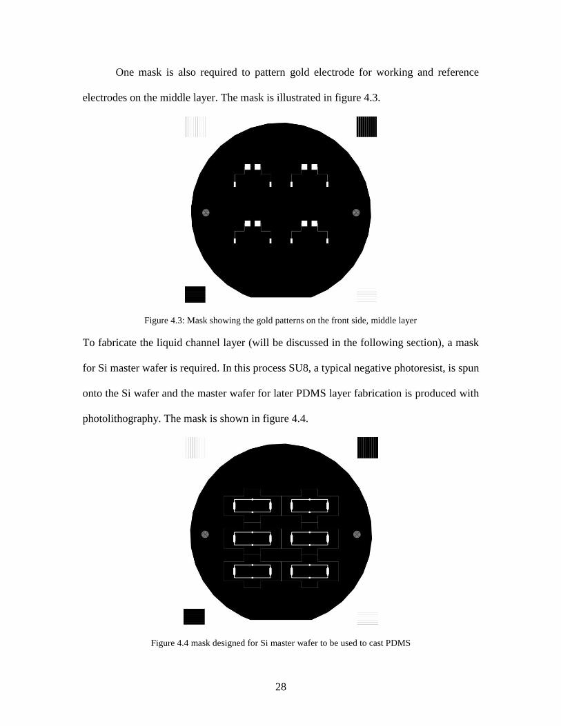
One mask is also required to pattern gold electrode for working and reference
electrodes on the middle layer. The mask is illustrated in figure 4.3.
Figure 4.3: Mask showing the gold patterns on the front side, middle layer
To fabricate the liquid channel layer (will be discussed in the following section), a mask
for Si master wafer is required. In this process SU8, a typical negative photoresist, is spun
onto the Si wafer and the master wafer for later PDMS layer fabrication is produced with
photolithography. The mask is shown in figure 4.4.
Figure 4.4 mask designed for Si master wafer to be used to cast PDMS

29
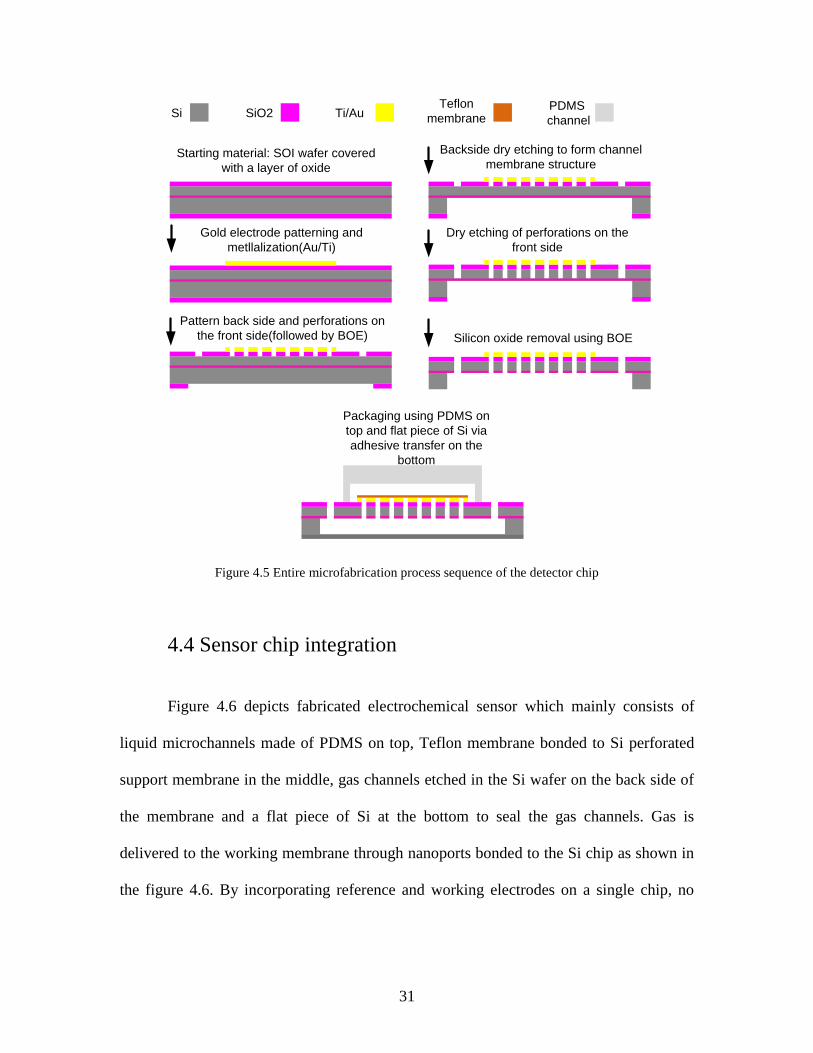
4.3 Microfabrication process sequence
The entire microfabrication process sequence of the detector chip is summarized
in figure 4.5. A three-mask process is used to produce the bottom half of the device. A
SOI Si wafer (Ultrasil, 20 μm device layer, 300 μm handle layer, 0.5 μm BOX)
preferably double side polished was used to fabricate the sensor chip. A 0.5 μm of SiO2
was grown in tube furnace using dry oxidation technique to electrically insulate the gold
electrode from Si substrate. A sputtered deposited Au/Ti film and a standard lift off
process are subsequently used to pattern gold electrodes (working and reference) on the
wafer front side. To promote adhesion a 100 Å Titanium is used under gold layer.
The front and back side of the wafer are patterned via double side
photolithography followed by dry etching of Si with Bosch process using ICP-DRIE
machine (SLR 770, Plasma-Therm). To prevent features from distortion if PR is etched
away during long etching process, additional protective layers of Chromium and
Aluminum are deposited on front and back sides of the wafer, respectively. Back side is
first etched away to form the gas channels followed by making perforated Si membrane
in DRIE. Wet buffered oxide etch (BOE) is used to remove the SOI layer in perforations.
A flat Si piece is bonded to the back side of the wafer using an intermediate adhesive
layer. The adhesive is typically an epoxy, which can be either cured by exposure to UV
light or by heating1. To provide consistent gas flow through channels, inlet/outlet gas
access holes are attached to nanoport assemblies (Upchurch Scientific) via adhesive ring.
Adhesive ring and nanoport assembly are aligned carefully to the drilled holes in Silicon
and clamped to be cured at 177°C for 1 hr.

30
The oxime aqueous solution flows through the second channel which is formed by
bonding PDMS microchannels to the top side of the device. The PDMS channel in the
device is fabricated using a molding process. First, negative photoresist, SU8-2100
(MicroChem Corporation, Newton, MA) was used to fabricate master of liquid
microchannels via standard photolithography. The spinner speed was adjusted to result in
the positive features with 150 μm height. Negative relief features in PDMS were obtained
by replica molding2, 3
. Inlet and outlet holes are then drilled in PDMS.
Gold is deposited onto the Teflon nanoporous membrane with a thin Ti film
serving as an adhesion layer. This membrane is sandwiched between the Si membrane
and the PDMS microchannel layer on top of the device. The composite membrane design
enhances the stability of gas-liquid interface as well as sensitivity of detection through
reducing diffusion time of electroactive species (to be described in the following
sections).
Both the Si sensor chip and the PDMS were exposed to oxygen plasma treatment
for 5 min to help permanently bond the liquid layer channel to the Si membrane. PDMS
channels width is wider than the Si membrane, leaving room for error in misalignment.
After bonding, the chip was cured at 60 °C for half an hour.
Gas permeability of polymeric channel does not allow it to be used in the final
design. Nonetheless they offer attractive features which can be utilized in early stages of
device development. These features include low cost, ease of manufacture and optical
transparency, enabling visual inspection of the membrane even after the whole device is
assembled4.
31
SiO2Si Ti/Au
Starting material: SOI wafer covered
with a layer of oxide
Gold electrode patterning and
metllalization(Au/Ti)
Pattern back side and perforations on
the front side(followed by BOE)
Backside dry etching to form channel
membrane structure
Dry etching of perforations on the
front side
Silicon oxide removal using BOE
Packaging using PDMS on
top and flat piece of Si via
adhesive transfer on the
bottom
Teflon
membranePDMS
channel
Figure 4.5 Entire microfabrication process sequence of the detector chip
4.4 Sensor chip integration
Figure 4.6 depicts fabricated electrochemical sensor which mainly consists of
liquid microchannels made of PDMS on top, Teflon membrane bonded to Si perforated
support membrane in the middle, gas channels etched in the Si wafer on the back side of
the membrane and a flat piece of Si at the bottom to seal the gas channels. Gas is
delivered to the working membrane through nanoports bonded to the Si chip as shown in
the figure 4.6. By incorporating reference and working electrodes on a single chip, no

32
separate reference electrode (such as Ag/AgCl) is necessary for open circuit potential
measurements.
Figure 4.6: Photograph of assembled sensor chip developed for detection of hazardous compounds
Figure 4.7 shows an SEM image of Si perforated membrane on the middle layer.
The pores are 30 μm in diameter. The gas channel and reaction chamber are also clearly
shown. The width of gas channel is 100 μm and the reaction chamber is a 800μm × 2500
μm rectangle. Figure 4.8 depicts the cross section of the Teflon membrane bonded to the
perforated Si membrane. The Teflon nanoporous membrane is 50 μm thick and consists
of pure PTFE laminated to a polypropylene support for improved durability and easy
handling.

33
Figure 4.7: Top view of the Si perforated membrane
Figure 4.8: Cross sectional view of the perforated Si membrane with Teflon membrane bonded on top.
4.5 Microreactor Simulation modeling with COMSOL 3.4
Although the liquid was gently injected into the microchannel and was stagnant
during the experiment, liquid leakage into gas chamber was the main issue associated

34
with the Si perforated membrane with 30 μm diameter as it tested without having a
nanoporous membrane. In the experiments, nanoporous Teflon membrane (purchased
from GE Osmonics' Labstore) bonded to the Si perforated membrane enhanced the
stability of the gas and liquid interface. It was thought that using composite nanoporous
membrane not only avoids liquid leakage into the gas channel but also improves
sensitivity of detection through reducing diffusion time of electroactive species (cyanides
ions). We were unable to prove this hypothesis experimentally as all experiments with
perforated Si membrane failed due to liquid leakage. Therefore, finite element method
software FEMLAB 3.4 (COMSOL, Stockholm, Sweden) has been employed to
investigate the performance of the detector with and without nanoporous membrane. A
simple 2D model of the vapor and liquid micro-channels is shown in figure 4.9.
Gas channel outletGas channel inlet
Teflon nanoporous
membrane
Liquid channel
Figure 4.9: Two dimensional model of the vapor and liquid micro-channels in COMSOL
First, coupled incompressible Navier-Stokes equation (eqn (1)) and continuity
equation (eqn (2)) were solved in steady state manner in the gas channel.
T
u u u u p F (1)
0u (2)
In these equations, μ is the viscosity, u the velocity, ρ the density, p the pressure,
F the sum of the body forces. The fluid (He carrier gas) density (ρ) was set to 0.164
kg/m3
and the fluid viscosity (μ) to 1.9×10⁻⁴
Pa.sec. For the Navier-Stokes equation, inlet

35
flow rate of 1 ml/min and flow rate at the outlet defined by the pressure equaling to zero
were used. On all other surfaces, the no slip boundary condition was used. The x and y
components of velocity profile in the gas channel was saved for solving convection and
diffusion equation as described below.
Mass balance equations (eqn(3)) in three domains (gas channel, Teflon membrane
and liquid channel) coupled with reaction kinetics in the liquid phase, assumed to be
second order (eqn (4)) were solved simultaneously in an unsteady state fashion upon
injection of the vapor pulse.
ii i
cD c R u c
t
(3)
*
AA OxR k c c (4)
In these equations, D is the diffusion coefficient for each three phases, k reaction
rate constant, ci the concentration of compounds and u is the velocity. The velocity is
given by the stationary solution of Navier-Stokes equations. There are four main
compounds in the system with assigned concentrations, CAA (acetic anhydride in the gas
phase), C*
AA(dissolved acetic anhydride in the liquid), Cox(oxime compound
concentration in the liquid and CCN-(cyanide ion concentration in the liquid phase). Acetic
anhydride is injected into the vapor microchannel and reacts with an alkaline oxime
solution as it dissolves in the liquid phase, which implies a concentration discontinuity at
the porous membrane-liquid interface. It’s assumed that acetic anhydride in the gas and
liquid phase reach equilibrium rapidly and Henry’s law constant has been used to
determine acetic anhydride concentration in liquid upon reaction. C*AA is the
concentration of dissolved acetic anhydride. In eqn (3) reaction terms in gas and
membrane phases are zero and all convective transport terms in membrane and liquid

36
phases are zero. The diffusion coefficients, Dg (of acetic anhydride in gas), Dm (of acetic
anhydride in the Teflon membrane) and Dl (of any species in the liquid phase) were set to
3.86×10⁻⁵
, 2.4×10⁻⁵
and 1×10⁻⁹
m2sec
-1, respectively. Henry’s law constant for acetic
anhydride5 was set to 1.353×10
5 and k
6 to 90 m
3mol
-1 sec
-1.
We defined the time-dependant inlet boundary condition inlet as a Gaussian pulse
with the maximum concentration of 4.46×10⁻⁶
M and width of 0.1 sec at half height.
Initial concentration of oxime in the liquid phase was set to 5 mM. In the gas channel the
exit boundary condition was set to convective flux stating that all mass transport over the
boundary occurs through convection.
4.6 Conclusions
A silicon based gas-liquid interface membrane for oxime chemistry based
electrochemical sensor was successfully fabricated using MEMS techniques. All three
layers were integrated along with nanoport connectors. Herein, the design and fabrication
of the microdetector have been discussed and the challenges in design have been
determined. Two microchannels, one for oxime solution and the other for gas containing
the analyte of interest are the major components of the detector construction. Gas and
liquid channels interface has a dual role: stability of the interface and output signal
collector. Standard lithography, dry etching as well as wet chemistry techniques have
been utilized to fabricate the sensor. In order to determine some geometrical parameters
such as liquid depth and also gas-liquid interface properties, finite element method
software, COMSOL 3.4, has been used. A simple 2-D model representing the system of
interest was created in the software and transport phenomena in three domains (gas,

37
liquid and the membrane) were solved. The simulation results along with experimental
testing of the microdetector are presented in the next chapter.
4.7 References
1. Flachsbart, B. R.; Wong, K.; Iannacone, J. M.; Abante, E. N.; Vlach, R. L.;
Rauchfuss, P. A.; Bohn, P. W.; Sweedler, J. V.; Shannon, M. A., Design and
fabrication of a multilayered polymer microfluidic chip with nanofluidic
interconnects via adhesive contact printing. Lab on a Chip 2006, 6, 667–674.
2. Duffy, D. C.; McDonald, J. C.; Schueller, O. J. A.; Whitesides, G. M., Rapid
Prototyping of Microfluidic Systems in Poly(dimethylsiloxane). Analytical
Chemistry 1998, 70, 4974–4984.
3. McDonald, J. C.; Duffy, D. C.; Anderson, J. R.; Chiu, D. T.; Wu, H.; Schueller, O.
J. A.; Whitesides, G. M., Fabrication of microfluidic systems in
poly(dimethylsiloxane). Electrophoresis 2000, 21, 27-40.
4. Aleksander J. Franz; Jensen, K. F.; Schmidts, M. A. In Palladium based
micromembranes for hydrogen seperation and hydrogenation/dehydrogenation
reactions, Twelfth IEEE International Conference on Micro Electro Mechanical
Systems.
5. Sander, R. Henry's Law Constants (Solubilities). http://www.mpch-
mainz.mpg.de/~sander/res/henry.html
6. Ford, B. W.; Watts, P., Reaction of isopropyl methylphosphonofluoridate with 1-
phenylbutane-1,2,3-trione 2-oxime. Journal of the Chemical Society, Perkin
Transactions 2: Physical Organic Chemistry 1974, 9, 1009-13.

38
Chapter 5
Experimental testing of the fabricated microdetector
5.1 Introduction
In this chapter, Experimental testing of the detector along with the results of
simulation modeling in COMSOL 3.4 will be discussed. In the course of experiments the
liquid phase (oxime solution) remains stagnant while the carrier gas (Helium) is blowing
onto the membrane. The analyte of interest is injected to the sensor set-up using gas
chromatography unit (Agilent 6890 GC/MS) equipped with 7683B auto-sampler. The
sensor output is recorded as a difference in open circuit potential between working and
reference electrodes.
5.2 Materials and methods
5.2.1 Chemical preparation
Chemical structure of oxime and phosphorous compounds, PH, temperature and
type of solvent are the major factors affecting the rate of reaction between oxime and
phosphorous compounds1. In a previous work, we have shown that using 1-phenyl-1, 2,
3,-butanetrione 2-oxime (PBO) oxime compound in PH 10 borate buffer gives the rapid
biggest potential change 2. To make borate buffer solution, 25 mM NaB4O7·10H2O
(Fisher) is dissolved, and the solution pH is adjusted by adding concentrated NaOH. Due
to oxime compound degradability over time and therefore less reactivity toward the target
molecule, the fresh solution is prepared for each run of experiments. The oxime solution

39
is 5 mM (1 mg/ml) 1-phenyl-1, 2, 3,-butanetrione 2-oxime (PBO, Aldrich) in PH 10
borate buffer.
In the course of experiments, we used an OP stimulant (acetic anhydride) to test
the sensor. The structure of acetic anhydride is similar to that of acetylcholine; in
particular it binds strongly to acetylcholinesterase. Previous work from our laboratory
has shown that the response of our sensors to acetic anhydride tracks the response to a
number of organophosphorous pesticides3, 4
.
5.2.2 Experimental set-up
The chemical vapors which are passed along the gas microchannel are sampled
from pure liquid chemical and automatically diluted to the desired vapor concentration
using split injection mode of gas chromatography unit (Agilent 6890 GC/MS) equipped
with 7683B auto-sampler.
The temperature of GC unit was maintained on 40 °C and desired concentration
of analyte was injected into an inert carrier, He, stream to the micro-sensor in a controlled
way. The microsensor setup with amplifier and filter electronics run by 9 V battery was
placed in the GC oven and connected to the split inlet using Restek deactivated guard
columns with 0.15 mm inner diameter. The injector and oven temperature were held at
150°C and 40°C, respectively. The oxime solution is passed along the liquid
microchannels using a manually-operated syringe. Oxime liquid remains static during
electrochemical measurements. After each run, oxime is replaced by injecting fresh
oxime solution to avoid data interference. Reference and working gold electrode were

40
attached to the Solartron SI 1287 potentiostat to measure the open circuit potential upon
injection of vapor pulses of acetic anhydride.
5.3 Results and discussion
5.3.1 Experimental results
Response is measured as change in open circuit potential between the active and
reference membrane electrodes integrated on a single chip. GC auto-sampler enabled us
to inject the desired amount of vapor concentration using split mode injection as most of
vaporized sample goes to split vent. The responses of our previously reported detector
fabricated in polycarbonate5 and this newly assembled microdetector fabricated in Si for
4.6×10¹⁰
injected molecules are shown in figure 5.1 for the sake of comparison.
Polycarbonate is not totally inert to phosphorus compounds and adsorption of target
molecule to polycarbonate channels causes decreases in sensitivity of the device. It can
be seen that fabrication of the sensor in Si shows a drastic improvement in the sensor
response.

41
0 3
0
5
10
Re
sp
on
se
(m
V/s
ec
)
Time (sec)
Polycarbonate Sensor
Silicon Sensor
Figure 5.1: Comparison between the responses of our previously reported detector fabricated in
polycarbonate5 and the newly assembled microdetector fabricated in Si for 4.6×10
10 injected molecules, no
amplifier or filter used.
Figure 5.2 shows the raw data obtained for different concentration of acetic anhydride
pulses injected to the Micro-sensor set up which correspond to different number of
molecules. The figure legend indicates the split ratio that has been used in the
experiments to achieve the desired number of molecule injection. Data analysis has been
done using Origin Pro 8 software to filter out the noise and smooth the data.

42
50 100 150
0
100
200
300
400
500
Po
ten
tia
l(m
V)
time(sec)
3000
5000
6000
10000
15000
20000
25000
30000
37500
50 60 70 80 90 100-10
0
10
20
30
40
50
60
Pote
ntial(m
V)
time(sec)
Figure 5.2: Raw output signal of microdetector set-up for different concentration of acetic anhydride pulses
injected to the Micro-sensor set up. Figure legend shows the split value used in GC set-up to inject the
desired amount of the analyte.
Figure 5.3 illustrates the first derivative of the raw data for different concentration
of acetic anhydride pulses injected to the micro-sensor set up which correspond to
different number of molecules as indicated in the figure. When the target molecule
reaches the liquid-membrane interface, it reacts with oxime solution to form cyanide ions
which generates the potential difference between working and reference electrodes. The
actual output peak of the sensor (potential difference vs. time) rises up corresponding to
formation and accumulation of cyanide ions onto the gold membrane upon reaction
taking place, but then as cyanide ions diffuse away from the membrane surface, it falls
back down to reach the stable potential baseline again. Response is measured as change
in open circuit potential between the active and reference membrane electrodes integrated
on a single chip.

43
The figure inset also shows the sensor’s sensitivity to the lowest achievable
concentration of acetic anhydride with a gas chromatography unit (3.51×10⁹ injected
number of molecules). For the lowest concentration level, it clearly shows a very
discernible response with negligible noise compared to the signal. It implies that the
microsensor setup can be even used for detection of much lower concentration of target
molecules.
40 45 50 55 60 65 70
-100
0
100
200
300
400
500
600
700
800
40 42 44 46 48 50 52 54 56 58 60
0
10
20
Time(sec)
First
de
riva
tive(m
V/s
ec)
Time(Sec)
4.39E10
2.64E10
2.20E10
1.32E10
8.78E9
6.59E9
5.27E9
4.40E9
3.51E9
Fir
st
de
riv
ati
ve
(mV
/se
c)
Number of molecules injected: 3.51E9
Figure 5.3: First derivative of output signal of microdetector set-up for different concentration of acetic
anhydride pulses injected to the Micro-sensor set up which correspond to different number of molecules as
indicated in the figure.
The detection limit could be extrapolated from the figure above assuming the
signal to noise ratio of 3mV/sec. Therefore, the estimated detection limit will be 2.75×10⁹
number of molecules injected.

44
5.3.2 Simulation results
For further investigation of the obtained results, we carried out a systematic
numerical study to realize the role of the composite membrane in the sensitivity level of
our device. The simulation domain and governing equations were well described in the
previous chapter.
Teflon nanoporous membrane was simulated as a homogenous medium with
diffusion coefficient equal to 2.4×10⁻⁵
m2s
-1 from the equation
6
4
3m gasD D where ε is the
porosity of nanoporous membrane (0.7 from experimental value). Velocity profile in the
gas channel obtained from Navier-Stokes equation was saved and convection and
diffusion equations in three domains in an unsteady state fashion upon injection of the
vapor pulse were solved simultaneously.
Figure 5.4 illustrates the snapshot of the system at 0.2 sec where the maximum of
pulse reaches the inlet of the gas channel. As time elapses, the concentration distribution
develops to parabolic form as a result of established velocity profile in the gas channel.
The concentration pulse travels through the gas channel and due to concentration gradient,
it diffuses toward the membrane. The red arrows indicate the total flux of target
molecules toward the membrane as a result of concentration gradient.

45
Figure 5.4: The snapshot of the acetic anhydride concentration field at t=0.2 sec. pulse of acetic anhydride
enters in the gas channel and red arrows indicate the total flux of target molecules toward the membrane.
In the experimental set-up, the total concentration of adsorbed cyanide ions onto
the electrode reveals the response of the sensor in the form of potential difference. In the
simulation modeling, by defining the integration coupling variable c_int which integrate
cyanide ion concentration over the membrane boundary we obtained the accumulated
concentration of cyanide ions on the membrane surface vs. time. In the case that we have
Teflon membrane bonded to the Si perforated membrane, the integration is done over the
entire boundary where as in the case of Si perforated membrane, integration is carried out
only on the peripheral areas of pores. The result of two simulation modelings where it
enables us to compare the sensor response in two cases, with and without Teflon
membrane is shown in the figure below (see figure 5.5)

46
0.0 0.2 0.4 0.6 0.8 1.0 1.2 1.4 1.6
0.0
3.0x10⁻¹²
6.0x10⁻¹²
9.0x10⁻¹²
1.2x10⁻¹¹
1.5x10⁻¹¹
To
tal
cy
an
ide
s i
on
s c
on
ce
ntr
ati
on
on
ele
ctr
od
e(M
)
Time(Sec)
With Teflon membrane
Without Teflon membrane
Figure 5.5: Accumulated concentration of cyanide ions on the membrane surface vs. time. The result is
obtained by defining the integration coupling variables in two models where it integrates the cyanide ions
concentration over entire membrane boundary and over peripheral areas of the Si pores in with and without
Teflon membrane cases, respectively.
Comparing the two curves reveals that using nanoporous Teflon membrane
bonded to the Si perforated membrane tremendously enhances sensor response. As
mentioned earlier, target molecules diffuse into the liquid, chemical reaction takes place
and cyanide ions will form. If the ions upon formation instantly adsorb to the gold
electrode, the response is significant. But if they have to diffuse into the liquid to reach to
the electrode surface, the signal will be attenuated. Using nanoporous membrane
extremely reduces diffusion time of ions to reach to the electrode. As they form they are
adsorbed onto the electrode and accumulation of cyanide ions onto the gold electrode is
conducive to the abrupt change in open circuit potential. In the case of Si perforated
membrane, the ions formed need to diffuse in the liquid to reach to the gold electrode

47
deposited onto the peripheral areas of Si pores. Diffusion time can be calculated using
2
2 l
d
D where d is the diffusion distance and Dl is the diffusion coefficient
7. Therefore,
time required for the ions formed in the center of the pores to diffuse to the electrode
surface in micropore membrane and nanoporous membrane cases were calculated to be
0.11 sec and 5×10⁻⁶
sec, respectively. By employing FEMLAB simulation, we were able
to show that using composite nanoporous membrane not only avoids liquid leakage into
the gas channel in the experiment but also improves sensitivity of detection through
reducing diffusion time of electroactive species (cyanides ions).
Liquid channel depth is another major design parameter affecting the sensor
response that can be investigated with the model we defined in COMSOL software. The
micro-detector set up should be capable of multiple uses before it needs oxime solution
replacement. Figure 5.6 illustrates the results of performing simulations for several
different liquid depth channels.

48
0.0 0.2 0.4 0.6 0.8 1.0 1.2 1.4 1.6
0.00
3.50x10⁻¹²
7.00x10⁻¹²
1.05x10⁻¹¹
1.40x10⁻¹¹
To
tal
cy
an
ide
io
n c
on
ce
ntr
ati
on
on
th
e e
lctr
od
e(M
)
Time(sec)
25m
35m
50m
150m
300m
Figure 5.6: Sensor response for several different liquid channel depths, in shallow liquid channels the
sensor does not regenerate itself whereas in deep enough channels, it regenerates in couple of seconds after
injection and reaches the stable baseline.
As can be seen, in shallow liquid channels the sensor does not regenerate itself
whereas in deep enough channels, it regenerates in couple of seconds after injection and
reaches the stable baseline. However, at around 75 μm and above, change in liquid
channel does not affect much on the sensor response as the responses of 150 μm and 300
μm are hardly distinguishable (see figure 5.6). In a shallow liquid channel, as the cyanide
ions diffuse away, ions concentration is equilibrated within the liquid medium side faster
than that in a deep enough liquid channel. High enough liquid depth allows the sensor to
regenerate itself for multiple uses in couple of seconds.

49
5.4 Conclusion
Experimental and simulation results demonstrate that the silicon based micro-
detector proposed in this work can be a promising way to selectively detect ultra low
levels of hazardous materials. Instant adsorption of eletroactive species onto the surface
membrane electrode upon formation is a necessity to detect ultra low levels of target
materials. We have shown that Teflon nanoporous membrane in this work plays dual role
in the sensor performance: stability enhancement of gas-liquid interface and sensitivity of
detection.
5.5 References
1. Green, A. L.; Saville, B., Reaction of Oxime with
isoPropylMethylphosphonofluoridate. Journal of the Chemical Society 1956,
3887-3892.
2. Oh, I.; Masel, R. I., Electrochemical Organophosphate Sensor Based on Oxime
Chemistry. Electrochemical and Solid-State Letters 2007, 10, (2), J19-J22.
3. Monty, C. N. Biological Mimics: A New Paradigm in the Detection of Toxic
Compounds. University Of Illinois Urbana Champaign, Urbana-Champaign Il,
2009.
4. Monty, C. N.; Oh, I.; Masel, R. I., Enzyme-based electrochemical multiphase
microreactor for detection of trace toxic vapors. IEEE Sensors Journal 2008, 8,
(5), 580-586.
5. Oh, I.; Monty, C. N.; Masel, R. I., Electrochemical multiphase microreactor as
fast, selective, and portable chemical sensor of trace toxic vapors. . IEEE Sensors
Journal 2008, 8, (5), 522-526.
6. MILLINGTON, R. J., Gas Diffusion in Porous Media Science 1959, 130(3367),
100-102.
7. Squires, T. M.; Quake, S. R., Microfluidics: Fluid physics at the nanoliter scale.
Reviews of modern physics 2005, 77, (3), 977-1026.

50
Chapter 6
Concluding remarks and future direction
6.1 Concluding remarks
In this work we have demonstrated fabrication and testing of a microdetector for
detection of organophosphorus agents. The reaction of hydroxamic acids with
organophosphorus antiacetylcholinesterase in alkaline aqueous solutions has been used as
a selective way of detection. The production of cyanide ion in this reaction was an
electroactive marker for the presence of organophosphorus agents in the sample. This fact
could be electrochemically detected by an open circuit potential change between working
and reference electrode incorporated in a single chip. Two microchannels, one for oxime
solution and the other for gas containing the analyte of interest were the major
components of the detector construction. A Teflon nano-porous membrane in the middle
of channels on Si perforated membrane was used to enhance the stability of gas-liquid
interface as well as sensitivity of detection. Teflon membrane in between creates a
clearance which prevents complete binding between the Si chip and PDMS channel on
top. Substitution of composite membrane with a submicron holes membrane etched in Si
would eliminate the difficulties associated with packaging the chip with PDMS liquid
channels.
Experimental results demonstrate that the silicon based micro-detector proposed
in this work can be a promising way to selectively detect ultra low levels of hazardous
materials. The detection limit of this sensor design is in the parts per trillion levels or
approximately 2.75×10⁹ molecules.
51
In order to investigate the influences of important geometric parameters on
detector performance, a finite element based commercial software, COMSOL 3.4
(Stockholm, Sweden) has been utilized. A 2D simulation of the system consists of gas
and liquid micro-channels with a nanoporous gas-liquid interface. Coupled steady state
Navier-Stokes, continuity and unsteady state mass transfer equations with chemical
reaction have been numerically solved to establish a realistic model of the system.
Simulation results indicated that using a nanoporous gas-liquid interface tremendously
reduces diffusion time of cyanide ions, leading to a fast response of the detector
compared to micron size membrane. Furthermore, it has been shown that the liquid
channel depth and nanomembrane porosity are amongst the main parameters affecting the
micro-sensor performance.
6.2 Future direction
In order for the developed microdetector to move beyond laboratory tool, it must
be integrated with other μTAS components such as gas preconcentrator and separators
(e.g. microfabricated GC). To reach to this end, membrane with sub micron holes for gas-
liquid interface has to be fabricated in Si ship to eventually substitute composite
membrane design presented here. As mentioned earlier, it also circumvents the problems
associated with packaging of the device. There are several ways suggested in the
literature to create submicron patterns such as using electron beam lithography1, block
copolymer2, 3
and porous Si4, etc. Since the membrane here requires high aspect ratios in
the order of 400:1 to have enough mechanical stability in gas and liquid interface, the
porous Si option looks promising. However, there are still some issues need to be

52
addressed: since the membrane itself has to play dual roles as gas-liquid interface and
also as an electrode, deposition of gold should not block the pores but also provide
enough conductivity. One way to address this issue is to sputter thin layer of gold (10
nm) on the die after fabrication of porous Si and then mask all over the membrane area
but the edges to ensure it does not get deposited in the next run of sputtering gold. (See
figure1, step i) Continuing on the sputtering assures that it has enough connectivity for
measuring purposes. In the figure 6.1 the tentative plan to design and fabricate the micro-
detector is shown. Future research needs to be focused on how to fabricate a porous Si
membrane with the desired pore size and pores density for sensor applications4. Different
Parameters in anodization process allow us to acquire a range of nanopores
characteristics. Among the important ones are: HF concentration, current density and
characteristics of the Si wafer.
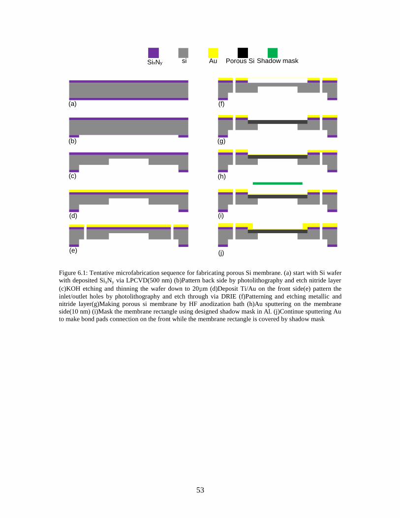
53
(a)
(b)
(c)
(d)
(e)
(f)
(g)
(h)
(i)
(j)
siSixNy Au Shadow maskPorous Si
Figure 6.1: Tentative microfabrication sequence for fabricating porous Si membrane. (a) start with Si wafer
with deposited SixNy via LPCVD(500 nm) (b)Pattern back side by photolithography and etch nitride layer
(c)KOH etching and thinning the wafer down to 20μm (d)Deposit Ti/Au on the front side(e) pattern the
inlet/outlet holes by photolithography and etch through via DRIE (f)Patterning and etching metallic and
nitride layer(g)Making porous si membrane by HF anodization bath (h)Au sputtering on the membrane
side(10 nm) (i)Mask the membrane rectangle using designed shadow mask in Al. (j)Continue sputtering Au
to make bond pads connection on the front while the membrane rectangle is covered by shadow mask

54
6.3 References
1. Madou, M., Fundamentals of Microfabrication: The Science of Miniaturization,
Second Edition. 2 ed.; CRC press: Boca Raton, FL, 2002.
2. Harrison, C.; Park, M.; Chaikin, P. M.; Register, R. A.; Adamson, D. H.,
Lithography with a mask of block copolymer microstructures. Journal of Vacuum
Science & Technology B: Microelectronics and Nanometer Structures 1998, 16,
(2), 544-552.
3. Park, M.; Harrison, C.; Chaikin, P. M.; Register, R. A.; Adamson, D. H., Block
Copolymer Lithography: Periodic Arrays of ~1011
Holes in 1 Square Centimeter.
Science 1997, 276, (5317), 1401 - 1404.
4. Taliercioa, T.; Dilhanb, M.; Massonea, E.; Guéc, A. M.; Fraissed, B.; Foucaran,
A., Realization of porous silicon membranes for gas sensor applications. Thin
Solid Films 1995, 255, (1-2), 310-312.

55
Appendix A: Fabrication procedures
A.1 Sensor chip fabrication
Thermal oxidation
1. Dry oxidation in furnace to get 500 nm of oxide on the SOI wafer.
Create gold contacts 2. Degrease the wafer (acetone, IPA, DI, IPA, N2 dry)
3. Bake out wafer on hotplate at 150C for 2 min.
4. Spin coat AP8000 promoter (recipe 3, 3000rpm, 30 sec)
5. Spin coat pore side of wafer with PR1518(recipe 3, 3000rpm, 30 sec)
6. soft bake on Al ring 3 minutes 110 C with heat shield
7. expose mask #1 (20 sec exposure) using aligner preset#3
8. develop in AZ400 K developer (4:1 developer, 100 ml DI) about 90 sec
9. DI quench then rinse low pressure DI, N2 dry
10. check with microscope for developing result
11. hard back 30 sec at 110 C
12. sputter Ti for 10 nm at 300 W
13. sputter Au for 100 nm at 300 W
14. lift off in 1165PR stripper in ultrasound for at least 15 min then DI rinse, then
transfer
15. acetone bath in ultrasound for 2 min, IPA bath in ultrasound for 2 min N2 dry
16. Check with the microscope and make sure there are no remaining particles
Double side lithography
17. Spin coat top side with AP8000 promoter and PR 4620 (recipe 3, 3000rpm, 7-
9μm)
18. Soft bake 60C/1min, 110C/1min
19. Spin coat PR 4620 on the back side (recipe 3, 3000rpm, 7-9μm)
20. Soft bake 60C/1min, 110C/1min
21. flip wafer and soft bake at 110 C for 2 min
22. Do lithography for the pore side. Expose with make #2on top, 20 sec in aligner
23. develop alignment marks in AZ400Kdeveloper(4:1 of DI/developer )
24. Do lithography for the gas channel side with back alignment. Expose with make
#3, 20 sec in aligner
25. develop entire wafer in AZ400K 1:4 for 3 min
26. DI quench for at least 1 min and N2 blow dry
27. Wet etch Al with etchant
28. Wet etch Au with etchant
29. Wet etch Ti with etchant
30. Freon RIE to SiO2

56
Etching in DRIE
31. hard back on hotplate at 110 C for 2 min with heat shield
32. Set hotplate at 160C and begin timing when hotplate reaches 150C for 5 min.
33. ICP-DRIE, using Recipe BOSCH-1 on the back side(gas channel first) Abort the
process at the end of etch step to prevent the top surface from getting covered
with PTFE.
34. ICP-DRIE, using Recipe BOSCH-1 on the pore side. Abort the process at the end
of etch step to prevent the top surface from getting covered with PTFE.
35. Cleaning up the channels by etching 2min additionally. This additional etching is
required to clean up the residues which were deposited during etching the other
side (pore side).
36. Strip photoresist in 400T at 125C for 15 min, ultrasound for 5 min with heat on,
DI quench.
37. Wet etch Cr etchant
38. Acetone bath in ultrasound for 2 min, IPA bath in ultrasound for 2 min, N2 dry.
Adhesive bonding afterwards
A.2 PDMS channel fabrication
SU8 Master Wafer fabrication
1. Clean the wafer
2. Prebake wafer for 5 min at 200 C
3. Dispense 4 ml of SU-2100 on the wafer
4. Ramp up to 500rpm @100rpm/sec
i. Hold for 5-10 sec
5. Ramp up to final speed(2000 rpm)@300 rpm/sec and hold for 30 seconds
6. Soft bake to evaporate solvents. Prebake @65C-5 min Softbake @95C-20 min
7. Expose for 11 sec (240 mJ/cm2/(21mW/cm
2)=11 sec)
8. Post exposure bake Prebake @65C-5min, Soft bake @95C-10-12 min
9. develop for 10-15 min
10. after development, the substrate should be rinsed briefly with IPA and then N2 dry
blow
11. Rinse tip: If a white film is produced during rinse, this is an indication that the
substrate has been under developed. Simply immerse or spray the substrate with
SU-8 developer to remove the film and complete the development process. Repeat
the rinse step
12. Hard bake the substrate for 5 min at 150 C
Transfer the SU8 master wafer to PDMS
1. Mix 50 gr of 184 silicon elastomeric base and 5 gr of curing agent in a plastic cup
using the scale

57
2. Stir the solution well enough for about 5 min by using a plastic spoon (5 min)
3. Place in the vacuum chamber and pump bubbles out(20 min)
4. Pour the solution on the Su8 master wafer until it covers the features.
5. Set the convection oven temperature at 60 C and check the level
6. Place the mold on it and cast the solution in the mold
7. Cover the solution and leave it overnight.

58
Appendix B: Adhesive Transfer technique
B.1 PDMS puck fabrication
8. Mix 50 gr of 184 silicon elastomeric base and 5 gr of curing agent in a plastic cup
using the scale
9. Stir the solution well enough for about 5 min by using a plastic spoon (5 min)
10. Place in the vacuum chamber and pump bubbles out(20 min)
11. Set the convection oven temperature at 60 C and check the level
12. Place the mold on it and cast the solution in the mold
13. Cover the solution and leave it overnight.
B.2 Recipe of bonding using adhesive
1. Drop much of VM652 adhesion promoter following by methanol on PDMS
2. Blow and dry the solution
3. Spin the adhesive on PDMS puck using recipe #1
4. Prepare a piece of glass on 50~ 60 C hotplates, put the sample on the glass.
5. Face the adhesive of PDMS down and contact the sample. Remove bubble from
the center to border if any. Count 3 min.
6. Prepare 2 cooling chucks. Leave the sample+pdms stack between them for 3 min.
7. Try to peel off pdms very smoothly, the adhesive is transferred.
8. Solvent vaporize on 110 for 1 min
9. Prepare the edge chuck on 110 C hotplate. Put the sample in the trench of the
chuck, align the sample
10. Once aligned, push the sample using the other end of the twizer. You can use the
Teflon or steel ball to promote the adhesion for 2 min
11. Put weight materials on the sample for keeping force on the sample
12. Increase temp to 140 C once 140 C hits count 15 min
B.3 D75 Adhesive recipe
1. Rinse 4 oz amber bottle with acetone and IPA and dry thoroughly with N2 gun
2. turn on weigh scale and tare with empty bottle placed on cellulose wipe
3. add first batch of ingredients
a. 0.1 gr Methylimidizole
b. 3.35 gr DEH 87
c. 8.35 gr DER 672
d. 32 gr Anisole
4. place clean magnetic stir bar in the bottle
5. Tighen up and place on stirrer at 300 rpm. Watch until stir bar can spin freely and
that no solid ”chunks” are stuck to the sides of the bottle

59
6. Mix on stirrer for at leat 20 hrs.
7. place in ultrasound for 5 min, making sure the top of the bottle is not submerged
8. add second batch of ingredients
a. 20 gr 2- methoxyethanol
b. 5 gr PGMEA
9. repeat steps 5-7


