http://www.diva-portal.org This is the published version of a paper published in 2D Materials. Citation for the original published paper (version of record): Del, S K., Bornemann, R., Bablich, A., Schaefer-Eberwein, H., Li, J. et al. (2015) Optimizing the optical and electrical properties of graphene ink thin films by laser-annealing. 2D Materials, 2(1): 011003 http://dx.doi.org/10.1088/2053-1583/2/1/011003 Access to the published version may require subscription. N.B. When citing this work, cite the original published paper. Permanent link to this version: http://urn.kb.se/resolve?urn=urn:nbn:se:kth:diva-196129
Transcript
http://www.diva-portal.org
This is the published version of a paper published in 2D Materials.
Citation for the original published paper (version of record):
Del, S K., Bornemann, R., Bablich, A., Schaefer-Eberwein, H., Li, J. et al. (2015)Optimizing the optical and electrical properties of graphene ink thin films by laser-annealing.2D Materials, 2(1): 011003http://dx.doi.org/10.1088/2053-1583/2/1/011003
Access to the published version may require subscription.
N.B. When citing this work, cite the original published paper.
Permanent link to this version:http://urn.kb.se/resolve?urn=urn:nbn:se:kth:diva-196129
This content has been downloaded from IOPscience. Please scroll down to see the full text.
Download details:
IP Address: 130.237.22.54
This content was downloaded on 11/11/2016 at 17:38
Please note that terms and conditions apply.
You may also be interested in:
Achieving concentrated graphene dispersions in water/acetone mixtures by the strategy of tailoring
Hansen solubility parameters
Min Yi, Zhigang Shen, Xiaojing Zhang et al.
Scalable, printable, surfactant-free graphene ink directly from graphite
X Han, Y Chen, H Zhu et al.
Graphene oxide: from fundamentals to applications
F Perrozzi, S Prezioso and L Ottaviano
Nanoscale reduction of graphene oxide thin films and its characterization
M Lorenzoni, A Giugni, E Di Fabrizio et al.
Gamma ray–assisted irradiation of few-layer graphene films: a Raman spectroscopy study
D N Kleut, Z M Markovi, I D Holclajtner Antunovi et al.
Production of graphene by exfoliation of graphite in a volatile organic solvent
Eun-Young Choi, Won San Choi, Young Boo Lee et al.
Laser heat treatment of aerosol-jet additive manufactured graphene patterns
Elahe Jabari and Ehsan Toyserkani
Optimizing the optical and electrical properties of graphene ink thin films by laser-annealing
View the table of contents for this issue, or go to the journal homepage for more
2015 2D Mater. 2 011003
(http://iopscience.iop.org/2053-1583/2/1/011003)
Home Search Collections Journals About Contact us My IOPscience
1 University of Siegen, Institute of Graphene-basedNanotechnology, Hölderlinstr. 3, D-57076 Siegen, Germany2 University of Siegen, Institute ofHigh Frequency andQuantumElectronics,Hölderlinstr. 3, D-57076 Siegen, Germany3 KTH-Royal Institute of Technology, School of Information andCommunicationTechnology, Electrum229, SE-164 40Kista, Sweden4 University of Siegen, Institut ofMaterials Chemistry, Paul-Bonatz-Str. 9-11, D-57076 Siegen, Germany
AbstractWedemonstrate a facile fabrication technique for graphene-based transparent conductive films.Highlyflat and uniform graphene films are obtained through the incorporation of an efficient laserannealing techniquewith one-time drop casting of high-concentration graphene ink. The resultingthinfilms are uniform and exhibit a transparency ofmore than 85% at 550 nmand a sheet resistanceof about 30 kΩ/□. These values constitute an increase of 45% in transparency, a reduction of surfaceroughness by a factor of four and a decrease of 70% in sheet resistance compared to un-annealed films.
Graphene dispersions are potential candidates for avariety of applications in printed electronics and assurface coatings. Transparent conductors made fromgraphene dispersions showpromising properties com-pared to traditionally usedmetallic oxide thin films. Incontrast to many metal oxides, graphene-based trans-parent films are flexible, chemically stable and exhibituniformbroadband absorption/transmission. In addi-tion, their production may ultimately be more costefficient. Recently,many groups investigated transpar-ent graphene conductors made from graphene disper-sions by inkjet printing [1–3], vacuum filtration [4–6]and spray coating [7]. Here, we propose a laserannealing technique for the fabrication of high perfor-mance transparent conductive films made from gra-phene dispersion. This technique is simple, fast and ondemand in comparison with other methods com-monly used. In addition, this technique can be appliedfor lithographic definition of transparent thin filmconductors made from graphene ink. Uniform, trans-parent and conductive graphene thin films werefabricated by simple drop casting of graphene disper-sion combined with a laser annealing process. Thelaser annealing method is primarily investigated withdrop-casted graphene dispersions and its universalityis confirmedwith inkjet printed graphenefilms.
Graphene ink with multiple graphene layers wasproduced by a solvent exchange technique [8], where
graphite powders were first exfoliated in dimethylfor-mamide (DMF) and stabilized with ethyl cellulose.Then, DMFwas exchanged by terpineol to increase thegraphene concentration, as well as to adjust the inkviscosity and to reduce solvent toxicity [9]. The gra-phene concentration in the final inks is as high asaround 1 mgmL−1.
In order to form multilayer graphene films, thegraphene ink was dispersed on a glass slide by con-trolled drop-casting (1 μL droplets). The high-con-centration inks allow efficient fabrication of graphenefilms through one-time drop casting. After ink drying,the obtained films were baked at 400 °C for 30 min toremove the stabilizing polymer which is necessary toprevent graphene flake aggregation during ink drying.Subsequently, the films were treated by scanning witha continuous wave laser beam (500 mW, 532 nm)across the surface with a power density of55MW cm−2 for a duration of 1–4 ms and a spot sizeof 1 μm. Figure 1(a) shows a schematic of the lasertreatment process. In addition, this laser system wasset up to conduct Raman measurements to enablein situ characterization throughout the process, albeitat lower laser power.
The graphene thin films were characterized by acombination of optical microscopy, laser scanningmicroscope, scanning electron microscope (SEM),Raman spectroscopy and x-ray powder diffraction
OPEN ACCESS
RECEIVED
4December 2014
REVISED
16 January 2015
ACCEPTED FOR PUBLICATION
29 January 2015
PUBLISHED
20 February 2015
Content from this workmay be used under theterms of theCreativeCommonsAttribution 3.0licence.
Any further distribution ofthis workmustmaintainattribution to theauthor(s) and the title ofthework, journal citationandDOI.
(XRD). Moreover, the electrical properties and thetransparency of thefilmswere characterized.
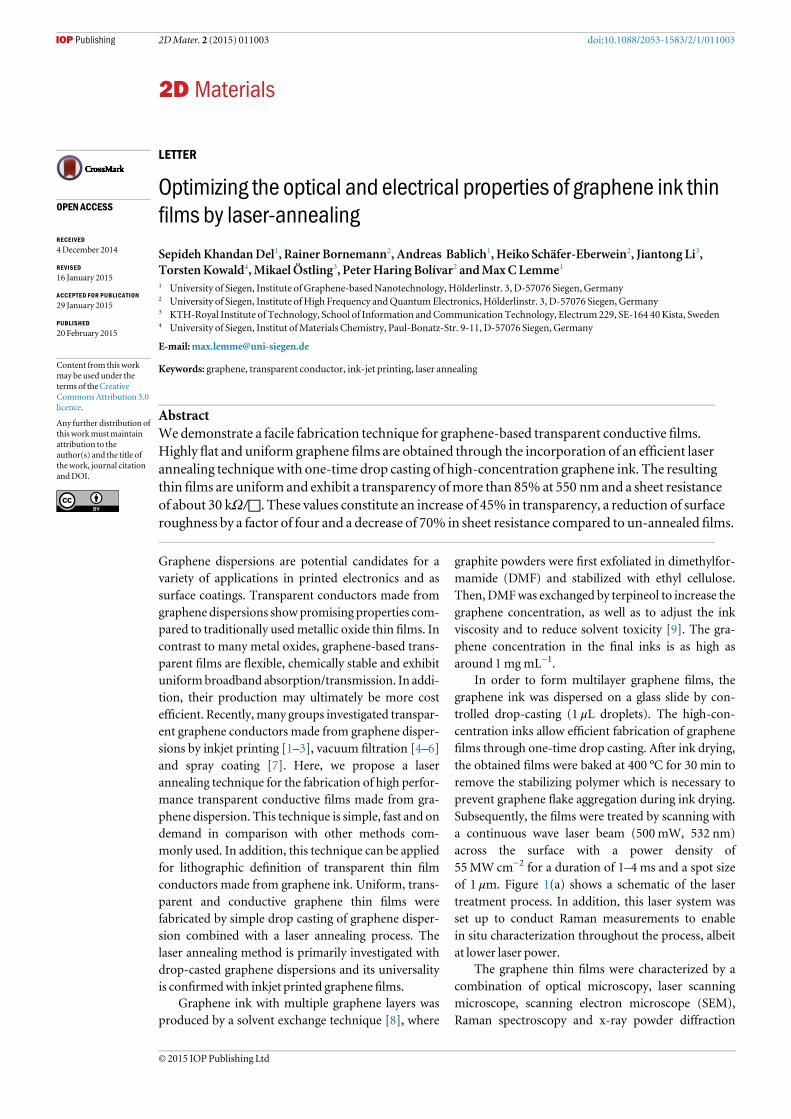
Figure 1(b) shows an optical micrograph of thefilm, including the areas where the laser annealingprocess was performed (marked by the dashed rec-tangles). In contrast to the untreated areas, the opticalimage shows improved transparency and homo-geneity after laser annealing.
The topography of the films was studied with aKEYENCE VK-X 200 laser scanning microscope(figure 1(c)). The roughness of the laser treated film(RRMS) is about 11 nm, which is about four timessmaller than that of as-deposited film (∼60 nm). Theaverage step height between the two areas infigure 1(c) is approximately 200 nm. These two resultsindicate a severe flattening effect of the laser annealingprocess on themultilayer grapheneflake film.
We carried out a systematic study of the influenceof the laser annealing power. Different areas of drop-casted graphene films were exposed to the laser withdifferent power and exposure times. The results areshown in figure 2(a), where the power ranges from55MW cm−2 to 17MW cm−2 and the exposure timeranges from 4ms to 1 ms. At 17MW cm−2, there is nooptically discernible effect of the laser on the film. Wetherefore chose to carry out Raman spectroscopy forboth annealed and un-annealed films at this laserpower. Figure 2(b) shows the average transmittancefor light with a wavelength of λ= 550 nm for the un-annealed (light blue background) and the annealed
regions of the film (patterned logo of the University ofSiegen). The transparency of the film increased from40% to over 85% after the laser annealing process.
SEM images (figure 3(a)) of annealed and un-annealed films were taken under a tilt angle of 52° toenhance surface topography. The insets show therespective regions with higher magnification. Theseimages demonstrate the topographical changes in thefilm due to the laser annealing process. In the annealedregion, graphene flakes are finer, smoother and morecompact, which results in a significantly improvedsurface homogeneity.
Figure 3(b) shows Raman spectra of the grapheneink drop-casted on a glass slide before and after laserannealing, but including thermal annealing at 400 °Cin both cases. In order to obtain Raman data for theun-annealed area, a low laser power was chosen, i.e.less than the threshold power required for a visibleannealing effect as discussed in figure 2. The spectraclearly show the signatures of graphitic films, i.e. the Gand the 2D bands. In addition, we observe D and D′intensities in the spectra. While the G peak is linked tothe relative motion of sp2 carbon atoms and indicatesthe presence of graphene, the D peak is due to thebreathing modes and requires defects for its activation(double resonance effect) [10–12]. The 2D peak is thesecond order of the D peak and is always seen even inthe absence of the D peak [11]. The origin of the D′peak is due to an intravalley double resonance effect[13]. Both the D and the D′ peak can be attributed to
Figure 1. (a) Schematic of the laser annealing process, where a green laser scans across the drop-castedmultilayer graphene film. (b)Opticalmicroscope image of as-deposited film, laser treated areas aremarked by dotted rectangle. The inset shows the border areawith highermagnification (c) 3D image of the surface topography by Laser scanningmicroscope, the step size between two dottedrectangles is around 200 nmwhich indicates the difference between average heights in the two areas.
2
2DMater. 2 (2015) 011003 SKDel et al
either the presence of a considerable amount of defectswithin the graphitic flakes or to disorder at the edges offlakes [13, 14]. The full-width at half-maximum of theG peak, FWHM(G), increases with structural disorder[15, 16]. Moreover, the intensity ratio I(D)/I(G)increases with increasing edge disorder [15]. There-fore, combining I(D)/I(G) with FWHM(G) can helpto discriminate between disorder localized at the edgesand disorder within the flakes. In the latter case, chan-ges in I(D)/I(G) would correlate with FWHM(G). Inthe laser annealed samples, both FWHM(G) and I(D)/I(G) decreased, from 40 cm−1 to 27 cm−1 and from0.62 to 0.34 respectively, indicating that the laserannealing process significantly reduces structural dis-order in the film.
XRD spectra were recorded to investigate the effectof the laser annealing on the structure of the film. Theresults are shown in figure 3(c). The peak at 2ʘ= 26.7°corresponds to the 002 plane of graphite layers with aninter-layer spacing of 0.334 nm. The intensity of thispeak is higher for laser treated samples, indicative of ahigher degree of graphene flake overlap in the (002)crystalline direction. This higher XRD count supportsthe hypothesis of a flattening effect of the laser anneal-ing process that was posed based on the SEM imagesand the laser scanningmicroscope data.
The sheet resistance of the graphene films wasassessed with a 4-point probe technique [17, 18]. Theun-annealed films exhibit a high sheet resistance ofapproximately 1 MΩ/□. The laser treatment process
Figure 2. (a)Opticalmicrograph of a drop-casted graphene film exposed to a laser (λ= 532 nm)with different power and exposuretime. (b) Laser lithography: transparencymap of the graphene film. The patternedUniversity of Siegen logo (red) represents the laserannealed filmwhile the background (green/blue) corresponds to the un-treated film.
Figure 3. (a) SEM image of treated and un-treated areas, the insets show the areas with highermagnification on the order of 150 000with horizontalfieldwidth on the order of 2 μm. (b) Raman Spectra of the un-treated (red) and the laser annealedfilm (black). Thefull-width at half-maximumof theGpeak and the intensity ratio ofD andGpeak decrease after laser annealing, indicating reducedstructural disorder after annealing. (c) XRDdiffractogramof laser annealed and un-treated films.
3
2DMater. 2 (2015) 011003 SKDel et al
reduces this value considerably by three to four ordersof magnitude to approximately 30 kΩ/□. We haveestablished by analytical methods that the laserannealing process results in a flattening effect of thegraphene layers. The considerable reduction of sheetresistance confirms this assessment: electrical trans-port in graphene films is dominated by the inter-flakejunction resistance and the number of junctions in thepercolation paths [19]. As the graphene films are flat-tened, the flake overlap/the junction area increases(compare SEM of untreated film in figure 3(a)) andthe inter-flake resistance decreases drastically. More-over, since most graphene lies flat on the substrate,much less flakes are needed to form a percolation path.As a result, the film sheet resistance is significantlydecreased.
In addition to flattening the graphene films, laserannealing may play a role in removing remainingpolymer (ethyl cellulose) trapped between the flakesby local heating. The heat flow in the cross-planedirection of the graphene layers and graphite flakes isstrongly limited by weak inter-plane van der Waalsforces. The drop-casted films mainly consist of ran-domly oriented graphene flakes. Therefore, in linewith the poor electrical conductivity, we conclude thatthe heat induced by the laser hardly dissipates, givingrise to a rapid local temperature increase in the film.
The removal of polymer likely contributes to thedramatic thickness decrease of the film after anneal-ing: there is a step of 200 nm between the laserannealed area and the un-annealed area in figure 1(c).Such a loss of material would certainly contribute toimproved transparency, in addition to an improve-ment due to better flake alignment and—conse-quently-reduced scattering. Polymer removal wouldalso contribute to a reduced sheet resistance in theflake percolation network.
Finally, the lasermay burn highly defective parts ofthe graphene flakes, since the experiments have beencarried out in ambient air. This would result in anoverall improved sheet resistance. Note that whilethere is no direct experimental evidence for this aspect,a chemical vapor deposited graphene film (withmuch less defects) was annealed by the laser in a
control experiment. This film did not change its con-ductive properties after annealing.
Figure 4(a) compares the sheet resistance andtransmittance of the drop-casted graphene filmsbefore and after laser annealing. The laser treatmentimproves both electrical and optical properties of thefilm significantly. In order to verify the universality ofthe laser annealing technique, we performed anexperiment on inkjet printed graphene films (6 print-ing passes) based on the same ink [2]. The result issimilar, if less pronounced, with a decrease in sheetresistance from ∼180 kΩ/□ to ∼60 kΩ/□ and anincrease in transmittance from 52% to 54%(λ= 550 nm).
The inkjet printed films are initially smoother andmore homogenous than drop casted samples. AFMmeasurements show an initial surface roughness forthe as printed sample of about 37 nm (RMS), and thisvalue drops to about 26 nm after laser annealing. Incontrast, the roughness (RMS) of drop casted samplesdropped from 53 nm to 22 nm through laser anneal-ing. This serves to explain the lower degree ofimprovement in the inkjet printed films, as these haveless potential for further improvement of the opticaland electrical properties.
Table 1 compares the sheet resistance and thetransparency of the reported graphene films atλ= 550 nm with literature data fabricated from gra-phene dispersion with variousmethods. These includeinkjet printing of graphene ink with further thermalannealing at 400 °C [2, 3], vacuum filtration through apolytetrafluoroethylene membrane [4] vacuum filtra-tion through mixed cellulose ester membranes (Milli-pore) and further annealing at 250 °C [5], vacuumfiltration with an alumina membrane followed bythermal annealing at 250 °C in argon atmosphere [6]and spray coating with subsequent thermal annealingat 250 °C in argon atmosphere [7] The films fabricatedby the method in this work exhibit electrical and opti-cal properties comparable to that of the state of the art.
In conclusion, we investigated transparent con-ductive graphene thin films fabricated by drop-castingof graphene ink, baking and subsequent annealingwith a scanning laser beam. The laser annealed films
90
80
70
60
50
40100 1000
Annealed
Annealed Un-Annealed Un-Annealed
Drop-casted sample
Printed sample
Sheet Resistance [kΩ/sq]
Tran
smis
sion
at 5
50 n
m [%
]
Figure 4.Optical transmission versus sheet resistance before and after laser annealing for drop casted (squares) and inkjet-printedgraphene films (dots).
4
2DMater. 2 (2015) 011003 SKDel et al
show low sheet resistance and high transmittance,which make them suitable candidates for electronicapplications such as transparent electrostatic dissipa-tion [20]. The laser annealing technique is transfer-rable to graphene inks obtained with other methods,as demonstrated with inkjet printed graphene films.This work introduces a fast, on-demand and econom-ical method to improve graphene ink properties andalso to controllably transform an insulating coatinginto a transparent conductive film. Moreover, it pro-vides the opportunity for large-scale fabrication and, ifa pattern generator is used, a basis for lithographicallydefined transparent conductors. Our workmay lead tothe development of a new generation of transparentconductive films with thermal and chemical stabilityand lowproduction cost.
Methods
The graphene inks were prepared through a solventexchange technique as detailed in Li et al [9] a mixtureof 2 mgmL−1 of natural graphite flakes (Sigma-Aldrich, Product No. 332461) andDMFwas sonicatedin a Branson 2510E-MTHbath ultrasonicator for 20 h,followed by centrifugation for 30 min at >10 000 rpmto sediment thick flakes. The supernatant was har-vested and a small amount of polymer (ethyl cellulose)was added to protect the graphene flakes fromagglomeration. The solution was then mixed withterpineol. A vacuum distillation process to ensure thatdistillation occurs at a temperature lower than thesolvents’ boiling points was used to remove DMF: thedispersion was heated to 80 °C in a water bath. As thepressure was reduced to 30 mbar, only the DMFevaporated. After the DMFwas boiled off, the remain-ing graphene/terpineol dispersion was harvested.Finally, a rough sonication for severalminutes sufficedto obtain pure, particle-free graphene dispersion.
The Raman spectra and the transmission imagewere taken with a self-built Raman micro spectro-meter, which can also be used for multispectral imageacquisition. The optical setup is built around a com-mercial inverted microscope (TE 300, Fa. Nikon). ForRaman excitation and the laser treatment, a green CWDPSS laser (532 nm, 500 mW, Fa. CNI) was used. Thelaser was coupled in the optical setup in the path forepi-fluorescence illumination. For multispectral
transmission imaging the original tungsten lamp wasused as a broad band light source. The spatiallyresolved spectra were taken with an imagingspectrograph and a liquid nitrogen cooled CCD cam-era (Triax 320 with a synergy CCD camera, Fa. HoribaJobinYvon). This detection part was attached to themicroscope at the back reflection port. For the anneal-ing and the imaging the samples were sampled step-wise with a motorized scanning stage (SCAN IM120× 100, Fa. Märzhäuser). The stepper motors ofthis microscope stage are trigged by the CCD camera,which acts as the master pixel clock for the completeimage acquisition.
Acknowledgments
The authors gratefully acknowledge funding by theEuropean Research Council through the Grant Inte-GraDe (No. 307311) and the Proof of Concept GrantiPUBLIC (No. 641416), as well as the GermanResearch Foundation (DFG, LE 2440/1-1, HA 3022/7-2), the Swedish Research Council through the grantiGRAPHENE, the Framework grant (No. 2014–6160)and the Göran Gustafsson Foundation through theYoungResearcher Prize (No. 1415 B).
References
[1] ShinKY,Hong J Y and Jang J 2011Adv.Mater. 23 2113[2] Li J, Ye F, Vaziri S,MuhammedM, LemmeMCandÖstlingM
2013Adv.Mater. 25 3985[3] Torrisi F et al 2012ACSNano. 6 2992[4] Parvez K, Li R, Puniredd SR,Hernandez Y,Hinkel F,Wang S,
FengX andMüllenK 2013ACSNano. 7 3598[5] Green AA andHersamMC2009Nano Lett. 9 4031[6] Hernandez Y et al 2008Nat. Nanotechnol. 3 563[7] Blake P et al 2008Nano Lett. 8 1704[8] Li J, Lemme M C and Östling M 2014 ChemPhysChem
15 3427[9] Li J, Ye F, Vaziri S,MuhammedM, LemmeMCandÖstlingM
2012Carbon 50 3113[10] Ferrari AC et al 2006Phys. Rev. Lett. 97 187401[11] Ferrari AC2007 Solid State Commun. 143 47[12] Tuinstra F andKoenig J L 2003 J. Chem. Phys. 53 1126[13] EckmannA, FeltenA,MishchenkoA, Britnell L, Krupke R,
Novoselov K S andCasiraghi C 2012Nano Lett. 12 3925[14] Casiraghi C, Pisana S,Novoselov K S, GeimAK and
Ferrari AC2007Appl. Phys. Lett. 91 233108[15] Canca̧do LG, Jorio A, Ferreira EHM, Stavale F, Achete CA,
Capaz RB,MoutinhoMVO, LombardoA, Kulmala T S andFerrari AC2011Nano Lett. 11 3190
Table 1.Comparison of the sheet resistance and transparency of conductive films fabricated fromgraphene dispersion.