13
*0DJD]]X· * $0DUFKLRURDQG30RUHLUD &(51(30,&*HQHYD6ZLW]HUODQG ,1)1²6H]LRQHGL3LVD3LVD,WDO\ December 6, 2001 7HFKQLFDOFRQWDFWSHUVRQHPDLO*XLGR0DJD]]X#SLLQIQLW
9������� �� �
����������*�������� ��������������������
����������������������������� ������!��"��������������#�����#����� $�
December 6, 2001
�
�
������������������������������������������������������������������������
%�� ���� ���������&��#�����'�� (��������������)&����*�����
9������� �� �
���+�%�%��+%����
�,������#���������##��������*�������#�� ����� ������#����*����� $�#��������#����-�-�
9������� �� �
�
,QWURGXFWLRQ� � '&8�$UFKLWHFWXUH� � 6SHFLILFDWLRQV� � '&8��,QWHUQDO�5HJLVWHUV� � 5HJLVWHU�'HILQLWLRQV� � &21752/�5(*,67(5��5�:�� � ([WHQGHG�&RQWURO�DQG�7HVW�5HJLVWHU��5�:��� $X[LOLDU\�5HJLVWHU��5�:�� � 6WDWXV��'DWD�+LJK�5HJLVWHU��5�:�� � 'DWD�/RZ�5HJLVWHU��5�:�� � '&8��2SHUDWLRQV� � +:�5HVHW� � 6:�5HVHW� � $FTXLUH� � 5HDG�5HVXOW� � '&8�&RQYHUVLRQ�2SHUDWLRQV� �� '&8��3LQ�/D\RXW��3DFNDJH�DQG�3LQ�$VVLJQPHQWV� �� '&8��3DG�$VVLJQPHQW� �� '&8��3DFNDJHG�9HUVLRQ� �� '&8��HYDOXDWLRQ�SDFNDJH� �� �
�
�
9������� �� �
�
�
& + $ 3 7 ( 5 � � �
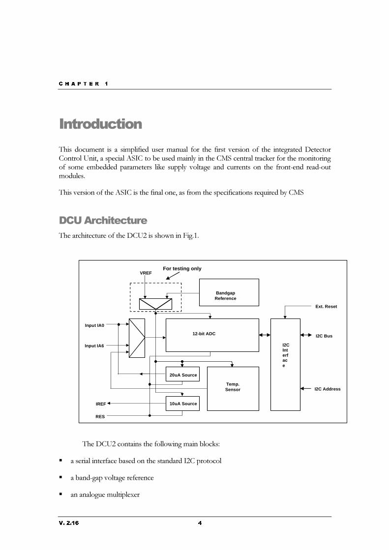
�����������
% �#� ����'���� �#� �� #�'& �*���� �#��� '���� � *��� � �� *��#�� ���#���� �*� � �� ����������� .�������������� �/�������#&���� ��������0���#���'��� $����� ������������ �����1���*���� ��'�����������*� #�'�� �'0������ &���'����#� �1�� #�&& $� �� ����� ���� �������#� ��� � �� *��������� ���������'��� �#���
% �#����#�����*�� �������#�� ��*��� �������#�*��'�� ��#&���*�������#���2������0$�����
�� �����������% ����� ����������*�� ��.�/,��#�# �������!���-��
�
% ��.�/,��������#�� ��*� ������'����0 ��1#(�
����#���� ������*����0�#������� ��#���������,��&������ �
����0������&��� �������*�������
�������� �����'� ��& �3���
12-bit ADC
BandgapReference
I2CInterface
Temp.Sensor
Input IA6
I2C Bus
VREF
Ext. Reset
IREF
RES
I2C Address
For testing only
Input IA0
20uA Source
10uA Source
9������� �� �
����-4�����#�������������#������
����-,�0���.��
��+�������������� ���5� ����/������� ���#� *��#�#�����#���#&���� �� ���� ���&�0 ��*�����#�����������&����� ��#����#��*�� ���� �����/�� ���� #6�
��������� �&���'&��������#��#���
����,4�����#�������������#�������#����� �0 ����������*�� ���� �����'��#���'������&���&��#��
% ������##����� ��������� �����#���#��*�� ��.�/��#����� �0 ��� ��� �����,�������*������% ���#�������#� ���������*�� ��.����&���� ���� #��#��������.����2��#���������������� ��.�����&���#�'& $�0$�����##������**�������,������#���#���
�0������&��� �������*�����������#����� ��.����#��0 ����*��������� ���������3����� ��� �����7��*� ���� 0�� �&& ���� ��� � �� .�/� ��#������*� � ���������������� *��'� � ��0������&� *��� ��#��&��&�#�#��� $��% ��.�/�&������#�����-4�����������,4�����������#�����#�� �������0���#�������������3����� �� ��'�#���#�*�����'&��������'��#���'�����
�������������.����� ������*������+(��,������������������ ���� �,�8�7���+�� ��� #�
��.���&���*�������#�
����&���� ���� #(�9�5�� $�:����� �0 �����&��1��������#���6�
����&��������(�,4�'7�→�;�,�8�7�������������#��
����*������� *��� �� ����� '��#���'���#(� ��.� ��� 7..� 5���������� ��� � �� #� �������&��������'���6�
����#� ������;�4�8�'7�
�����<�=��-�<�>���.�<�=��-�<�>�5'���������.������'�##��������#6�
��%���#���������#������=�4�8�<�>�
����3�������#����%�'��?�4�,8��#���
��+&����������'&�������������(��84���@�A84��
�����������#�'&����(�=�B4'C�
����&& $��� ����(�#��� ��7..�)�,�87�
��� ��1�*��2����$(�B4�D��
��.���#���(�,3,''�
9������� �� �
������*�&��#(�,9�5�� $�,B��#������&��1��������#���6�
����� �0 �����,B�&���<����&��1��������#���1��������
& + $ 3 7 ( 5 � � �
�� �����������������
���������������% ��.�/,��������#�� ��*� ������E�0���������� �����#���#(�
�������� �����#����� � � � 5����6�
���3� ���$�����#����� � � � 5���6�
��%�#������#����� � � � 5%���6�
�������#�F�.����D�� �����#������ 5�D���6�
��.����<�������#����� � � � 5<���6�
% ��������#���#�5��������������%���6�������CG�� ����'�����������5�D��������<���6������������ $���
% ������##����� ��B�����#���#�*� ��#�� ���,��#��������&������ ��% ��B���>#��*�� ��9�0����,�������##������#�����������##�� ��� �&��������,��0�#G�� ����'�������H�0��#������#�����������##�� ��*����������� �����#���#��������������� ��*� ��������0 �(�
Register I2C address <A2:A0>
CREG 000
AREG 010
TREG 100
SHREG 001
LREG 011
�
% ��*� ������##��*��� ����#���� �#� � ���*����������0$� � �����������������*� � �� �� �B��3����� $�#����0 �������##�#���� �� ��� ����������� �����#���������##��
#��#�� ��������,��0�#��*���0�� ������##����������� ����>��#�����#'������*��#���
9������� �� �
��������������� �!"#% ��0���� ���������*�� �������� �����#�����#���#���0���0� ��(�
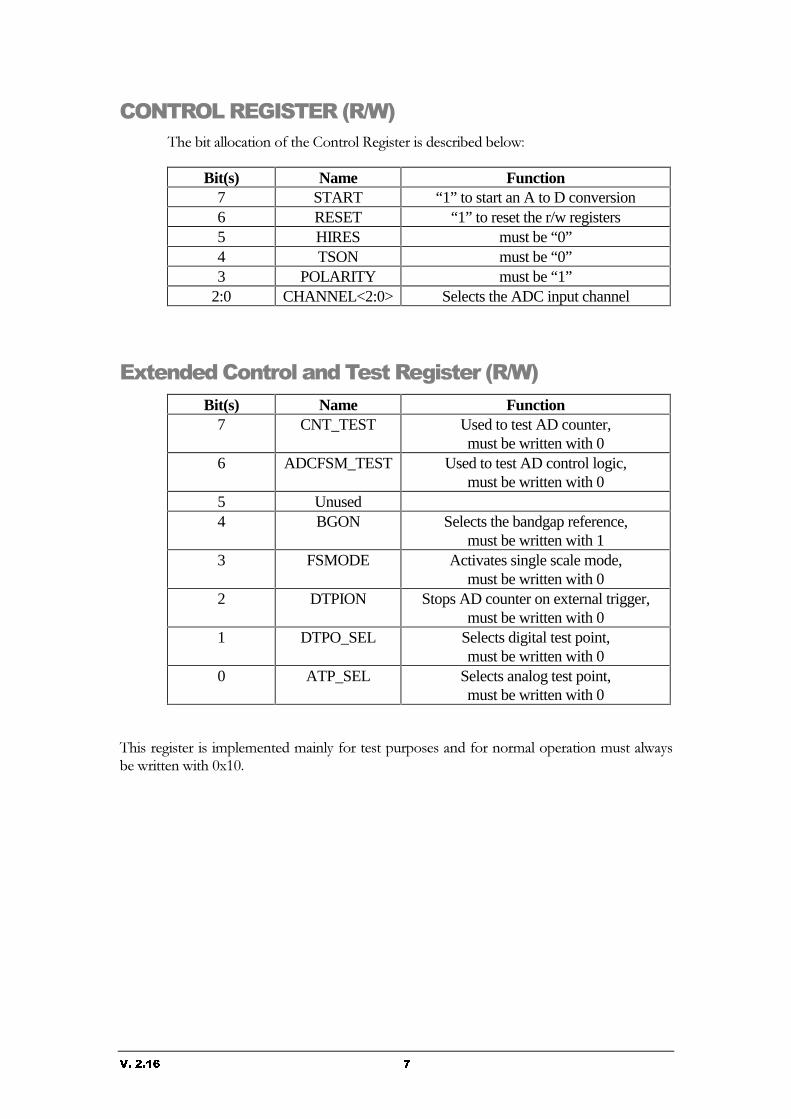
Bit(s) Name Function 7 START “1” to start an A to D conversion 6 RESET “1” to reset the r/w registers 5 HIRES must be “0” 4 TSON must be “0” 3 POLARITY must be “1”
2:0 CHANNEL<2:0> Selects the ADC input channel �
�$��������������������������� �!"#
Bit(s) Name Function 7 CNT_TEST Used to test AD counter,
must be written with 0 6 ADCFSM_TEST Used to test AD control logic,
must be written with 0 5 Unused 4 BGON Selects the bandgap reference,
must be written with 1 3 FSMODE Activates single scale mode,
must be written with 0 2 DTPION Stops AD counter on external trigger,
must be written with 0 1 DTPO_SEL Selects digital test point,
must be written with 0 0 ATP_SEL Selects analog test point,
must be written with 0 �
% �#�����#�����#��'& �'������'��� $�*�����#��&��&�#�#�����*������'� ��&��������'�#��� ��$#�0������������� �43-4��
9������� �� �
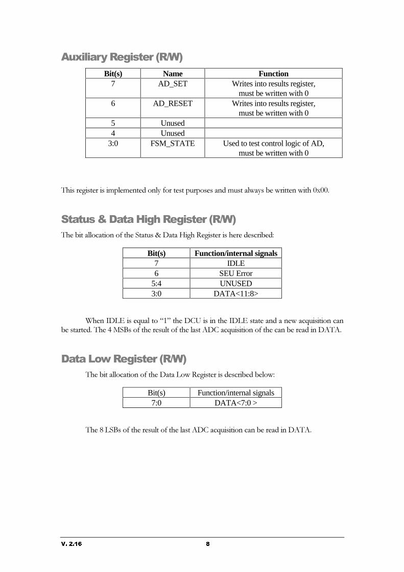
��$���%������� �!"#
Bit(s) Name Function 7 AD_SET Writes into results register,
must be written with 0 6 AD_RESET Writes into results register,
must be written with 0 5 Unused 4 Unused
3:0 FSM_STATE Used to test control logic of AD, must be written with 0
% �#�����#�����#��'& �'�������� $�*�����#��&��&�#�#�����'�#��� ��$#�0������������� �4344��
������&����'��������� �!"#% ��0���� ���������*�� �������#�F�.����D�� �����#�����#� ������#���0��(�
Bit(s) Function/internal signals 7 IDLE 6 SEU Error
5:4 UNUSED 3:0 DATA<11:8>
�
C ����.<���#��2�� ����I-J�� ��.�/��#����� ���.<��#�����������������2��#����������0��#��������% ��B���>#��*�� ����#� ���*�� �� �#��.����2��#�������*�� ������0����������.%��
������(������� �!"#% ��0���� ���������*�� ��.����<�������#�����#���#���0���0� ��(�
Bit(s) Function/internal signals 7:0 DATA<7:0 >
�
% ��E�<�>#��*�� ����#� ���*�� �� �#��.����2��#����������0����������.%��
�
�
9������� �� �
& + $ 3 7 ( 5 � � �
�� ����������
'"������ �������� ��#��� �*� � �� .�/,� ��C� ����#���#� �#� &��*��'��� *������� ��� I4J� � ��
����%�&�����
�"������#�*��������#����*�� ��.�/,���������#���#��#�&��*��'���� �����K-��#��������������� ��
0���:��*�� �������� �����#���������5����=:@6���
��)�������2��#�������#�#�������� �����K-� �#��������������� ��0���4��*�� �������� �����#����
�����5����=9@6��
% ��0�������=,(4@�#� ���#�� ����&���� ���� �������������� �� ��*� ��������0 �(�
CREG<2:0> ADC input channel 000 IA0 001 IA1 010 IA2 011 IA3 100 IA4 101 IA5 110 IA6 111 Temperature channel
����������C ���� ��0���4��*�� �������#�F�.����D�� �����#�����D���=9@��������#���K-��� ��
.�/-��#����� ���.<��#���������� ����#� ���*�� �� �#��.����2��#����������0������(�
�����=--(E@�?��D���=H(4@�
�����=9(4@�?�<���=9(4@�
�
9������� ��� �
�� ���*���������������������#�����$� ���*�� ��.������#�'& $�0��#�������0$�#�������� ��&��&���� ���� ������##����� �� ������ � ����#���� ���� #������� � �� #����� ������#���� 0��� ��� � �� #�'�� ����#����� % �� #�����������#���� 0��� 5�%�%6� �#� � ������ ����'����� $� ��� � �� ��'& ������ �*� � �� ������#����� !�����#������� �� ������#������� � �� ��&���� ���� �H�����0�� #�������0$�����������I--4--44-J� 5�����43.L6������� �������� �����#�����
& + $ 3 7 ( 5 � � �
�� �+���%���,+��-������+������.����
�� �+�������.���% ��.�/,�����#�����#�,�3�,�''G�� ��������,9����'� �&��#���� ���,,8�'�&��� �����H�
�3�����������&��#�*�����#�����&��&�#�#��� $���
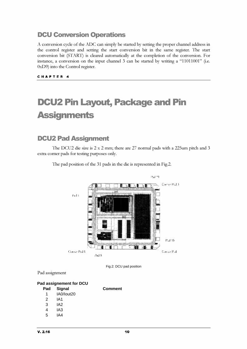
% ��&���&�#�������*�� ��H-�&��#����� �������#���&��#���������!���,��
�
Fig.2: DCU pad position
�����##���'����
Pad assignement for DCU Pad Signal Comment
1 IA0/Iout20 2 IA1 3 IA2 4 IA3 5 IA4
3DG���
3DG���
3DG����
3DG����
&RUQHU�3DG�&RUQHU�3DG���
&RUQHU�3DG���
9������� ��� �
6 IA5 7 IA6
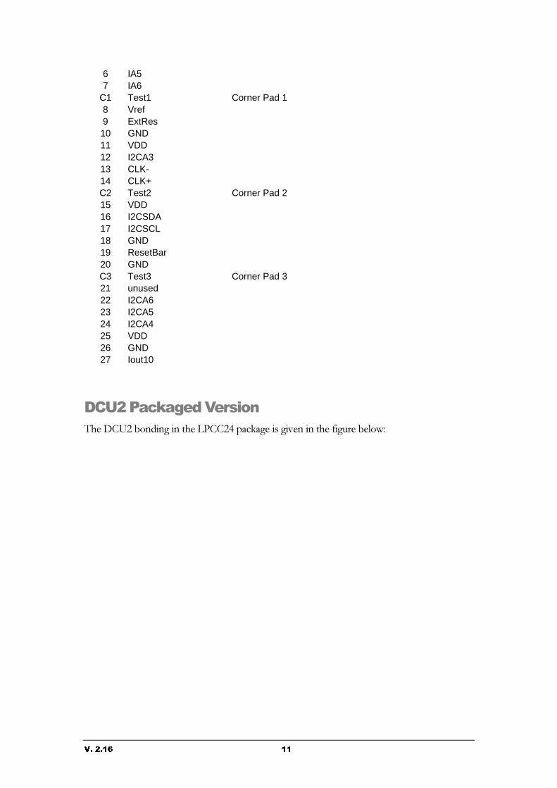
C1 Test1 Corner Pad 1 8 Vref 9 ExtRes 10 GND 11 VDD 12 I2CA3 13 CLK- 14 CLK+ C2 Test2 Corner Pad 2 15 VDD 16 I2CSDA 17 I2CSCL 18 GND 19 ResetBar 20 GND C3 Test3 Corner Pad 3 21 unused 22 I2CA6 23 I2CA5 24 I2CA4 25 VDD 26 GND 27 Iout10
�
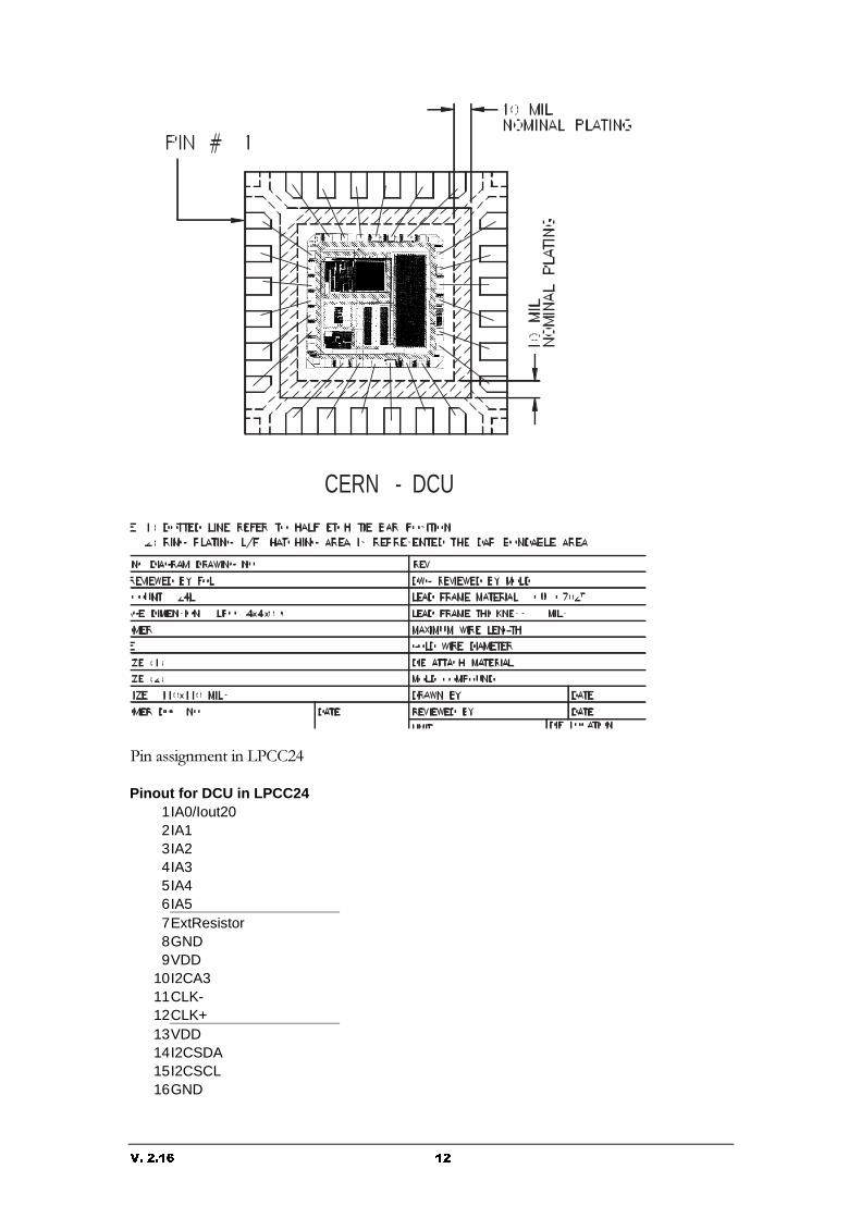
�� �+��-����/�����% ��.�/,�0����������� ��<���,B�&��1�����#����������� ��*������0� ��(�
9������� ��� �
CERN - DCU
�
�����##���'�������<���,B�
Pinout for DCU in LPCC24 1IA0/Iout20 2IA1 3IA2 4IA3 5IA4 6IA5 7ExtResistor 8GND 9VDD
10I2CA3 11CLK- 12CLK+ 13VDD 14I2CSDA 15I2CSCL 16GND
9������� ��� �
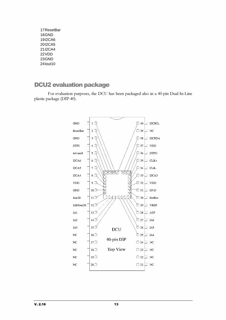
17ResetBar 18GND 19I2CA6 20I2CA5 21I2CA4 22VDD 23GND 24Iout10
�
�� ��*����������-���!������ �������&��&�#�#��� ��.�/� �#�0����&��1������ #�������B4�&���.�� ����<����
& �#����&��1����5.���B46���
�
��


