– EmbeddedICE-RT™ Logic for Real-Time• HighlightsDebug– High-Performance Digital Media
• ARM9 Memory ArchitectureSystem-On-Chip (DMSoC)– 16K-Byte Instruction Cache– Up to 216-MHz ARM926EJ-S™ Clock Rate– 8K-Byte Data Cache– Digital HDTV (720p/1080i) output for
connection to external encoder – 32K-Byte RAM– Video Processing Subsystem – 8K-Byte ROM
• Hardware IPIPE for Real-Time Image – Little EndianProcessing • Video Processing Subsystem
• Up to 14-bit CCD/CMOS Digital Interface – Front End Provides:• Histogram Module • Hardware IPIPE for Real-Time Image• Resize Image 1/16x to 8x Processing• Hardware On-Screen Display • Up to 14-bit CCD/CMOS Digital Interface• Up to 75-MHz Pixel Clock • 16-/8-bit Generic YcBcR-4:2 Interface
(BT.601)• Composite NTSC/PAL video encoderoutput • 10-/8-bit CCIR6565/BT655 Interface
– Peripherals include DDR and mDDR SDRAM, • Up to 75-MHz Pixel Clock2 MMC/SD/SDIO and SmartMedia Flash Card • Histogram ModuleInterfaces, USB 2.0, 3 UARTs and 3 SPIs • Resize Engine
– Enhanced Direct-Memory-Access (EDMA) – Resize Images From 1/16x to 8x– Configurable Power-Saving Modes – Separate Horizontal/Vertical Control– On-Chip ARM ROM Bootloader (RBL) to Boot – Two Simultaneous Output Paths
From NAND Flash, MMC/SD, or UART – Back End Provides:– 3.3-V and 1.8-V I/O, 1.3-V Core • Hardware On-Screen Display (OSD)– Debug Interface Support • Composite NTSC/PAL video encoder– Up to 104 General-Purpose I/O (GPIO) Pins output– 337-Pin Ball Grid Array at 65 nm Process • 8-/16-bit YCC and Up to 18-Bit RGB666
Technology Digital Output• High-Performance Digital Media • BT.601/BT.656 Digital YCbCr 4:2:2
System-on-Chip (DMSoC) (8-/16-Bit) Interface– 135-, 216-MHz ARM926EJ-S™ Clock Rate • Digital HDTV (720p/1080i) output for– Fully Software-Compatible With ARM™ connection to external encoder– Extended Temperature 135- and 216-MHz • External Memory Interfaces (EMIFs)
Devices are Available – DDR2 and mDDR SDRAM 16-bit wide EMIF• ARM926EJ-S Core With 256 MByte Address Space (1.8-V I/O)
– Support for 32-Bit and 16-Bit (Thumb Mode) – Asynchronous16-/8-bit Wide EMIF (AEMIF)Instruction Sets • Flash Memory Interfaces
– DSP Instruction Extensions and Single Cycle – NAND (8-/16-bit Wide Data)MAC – OneNAND(16-bit Wide Data)
Please be aware that an important notice concerning availability, standard warranty, and use in critical applications of TexasInstruments semiconductor products and disclaimers thereto appears at the end of this data sheet.
2Windows is a trademark of Microsoft.3All other trademarks are the property of their respective owners.
– Two Multimedia Card (MMC) / Secure Digital • Four Pulse Width Modulator (PWM) Outputs(SD/SDIO) • Four RTO (Real Time Out) Outputs
– SmartMedia • Up to 104 General-Purpose I/O (GPIO) Pins• Enhanced Direct-Memory-Access (EDMA) (Multiplexed with Other Device Functions)
Controller (64 Independent Channels) • On-Chip ARM ROM Bootloader (RBL) to Boot• USB Port with Integrated 2.0 High-Speed PHY from NAND Flash (with SPI EEPROM Boot
that Supports option), MMC/SD, or UART– USB 2.0 Full and High-Speed Device • Configurable Power-Saving Modes– USB 2.0 Low, Full, and High-Speed Host • Crystal or External Clock Input (typically
24 MHz or 36 MHz)• Three 64-Bit General-Purpose Timers (eachconfigurable as two 32-bit timers) • Flexible PLL Clock Generators
• One 64-Bit Watch Dog Timer • Debug Interface Support• Three UARTs (One fast UART with RTS and – IEEE-1149.1 (JTAG)
CTS Flow Control) Boundary-Scan-Compatible• Three Serial Port Interfaces (SPI) each with two – ETB™ (Embedded Trace Buffer™) with
Chip-Selects 4K-Bytes Trace Buffer memory• One Master/Slave Inter-Integrated Circuit (I2C) – Device Revision ID Readable by ARM
Bus® • 337-Pin Ball Grid Array (BGA) Package• Two Audio Serial Port (ASP) (ZCE Suffix), 0.65-mm Ball Pitch
– I2S and TDM I2S • 90nm Process Technology– AC97 Audio Codec Interface • 3.3-V and 1.8-V I/O, 1.3-V Internal– S/PDIF via Software • Community Resources– Standard Voice Codec Interface (AIC12) – TI E2E Community– SPI Protocol (Master Mode Only) – TI Embedded Processors Wiki
The DM335 processor is a low-cost, low-power processor providing advanced graphical user interface fordisplay applications that do not require video compression and decompression. Coupled with a videoprocessing subsystem (VPSS) that provides 720p display, the DM335 processor is powered by a135/216-MHz ARM926EJ-S core so developers can create feature-rich graphical user interfaces allowingcustomers to interact with their portable, electronic devices such as video-enabled universal remotecontrols, Internet radio, e-books, video doorbells, and digital telescopes. The new DM335 is packed withthe same peripherals as its predecessor, the TMS320DM355 device, including high-speed USB 2.0on-the-go, external memory interface (EMIF), mobile DDR/DDR2, two SDIO ports, three UART Ports, twoAudio Serial Ports, three SPI Ports, and SLC/MCL NAND Flash memory support. These peripherals helpcustomers create DM335 processor-based designs that add video and audio excitement to a wide rangeof today's static user-interface applications while keeping silicon costs and power consumption low. Thenew digital media processor is completely scalable with the DM355 processor and Digital Video EvaluationBoard (DVEVM), allowing customers to utilize their same code for their new DM335 processor focuseddesigns.
The new DM335 device delivers a sophisticated suite of capabilities allowing for flexible image captureand display. Through its user interface technology, such as a four-level on-screen display, developers areable to create picture-within-picture and video-within-video as well as innovative graphic user interfaces.This is especially important for portable products that require the use of button or touch screen, such asportable karaoke, video surveillance and electronic gaming applications. Additional advanced capture andimaging technologies include support for CCD/CMOS image sensors, resize capability and videostabilization. The 1280-by-960-pixel digital LCD connection runs on a 75-MHz pixel clock and supports TVcomposite output for increased expandability. This highly integrated device is packaged in a 13 x 13 mm,337 pin , 0.65 mm pitch BGA package.
The DM335 processor core is an ARM926EJ-S RISC processor. The ARM926EJ-S is a 32-bit processorcore that performs 32-bit and 16-bit instructions and processes 32-bit, 16-bit, and 8-bit data. The coreuses pipelining so that all parts of the processor and memory system can operate continuously. The ARMcore incorporates:• A coprocessor 15 (CP15) and protection module• Data and program Memory Management Units (MMUs) with table look-aside buffers.• Separate 16K-byte instruction and 8K-byte data caches. Both are four-way associative with virtual
index virtual tag (VIVT).
The DM335 device has a Video Processing Subsystem (VPSS) with two configurable video/imagingperipherals:• A Video Processing Front-End (VPFE)• A Video Processing Back-End (VPBE)
The VPFE port provides an interface for CCD/CMOS imager modules and video decoders. The VPBEprovides hardware On Screen Display (OSD) support and composite NTSC/PAL and digital LCD output.
The DM335 peripheral set includes:• An inter-integrated circuit (I2C) Bus interface• Two audio serial ports (ASP)• Three 64-bit general-purpose timers each configurable as two independent 32-bit timers• A 64-bit watchdog timer• Up to 104-pins of general-purpose input/output (GPIO) with programmable interrupt/event generation
modes, multiplexed with other peripherals• Three UARTs with hardware handshaking support on one UART• Three serial port Interfaces (SPI)• Four pulse width modulator (PWM) peripherals• Four real time out (RTO) outputs
DMA /Data and configuration busDMA/Data and configuration bus
DDR
MH
z )
DDRcontroller
DLDLL/PHY
16 bit
32bit Configuration Bus
CCDCIPIPE
VPBE
Vide
oEncod
er
VideoEncoder
10bDAC OS
D
OSD
erc
ARMARM INTC
Enhanced
channels3PCC /TC
(100 MHz
Enhanced DMA64 channels
Composite video
Digital RGB/YUV
Nand /Nand/SM/Async/One Nand
(AEMIF)
USB 2.0USB2.0 PHY
Speakermicrophone
ASP (2x)
Bu
ffe
r L
og
ic
VPSS
MMC/SD (x2)
SPI I/F (x3)
UART (x3)
I2C
Timer/WDT (x4 - 64)
GIO
PWM (x4)
RTO
VPFE
TMS320DM335
SPRS528C–JULY 2008–REVISED JUNE 2010 www.ti.com
• Two Multi-Media Card / Secure Digital (MMC/SD/SDIO) interfaces• Wireless interfaces (Bluetooth, WLAN, WUSB) through SDIO• A USB 2.0 full and high-speed device and host interface• Two external memory interfaces:
– An asynchronous external memory interface (AEMIF) for slower memories/peripherals such asNAND and OneNAND,
– A high speed synchronous memory interface for DDR2/mDDR.
For software development support the DM335 has a complete set of ARM development tools whichinclude: C compilers, assembly optimizers to simplify programming and scheduling, and a Windows™debugger interface for visibility into source code execution.
1.3 Functional Block Diagram
The below figure shows the functional block diagram of the DM335 device.
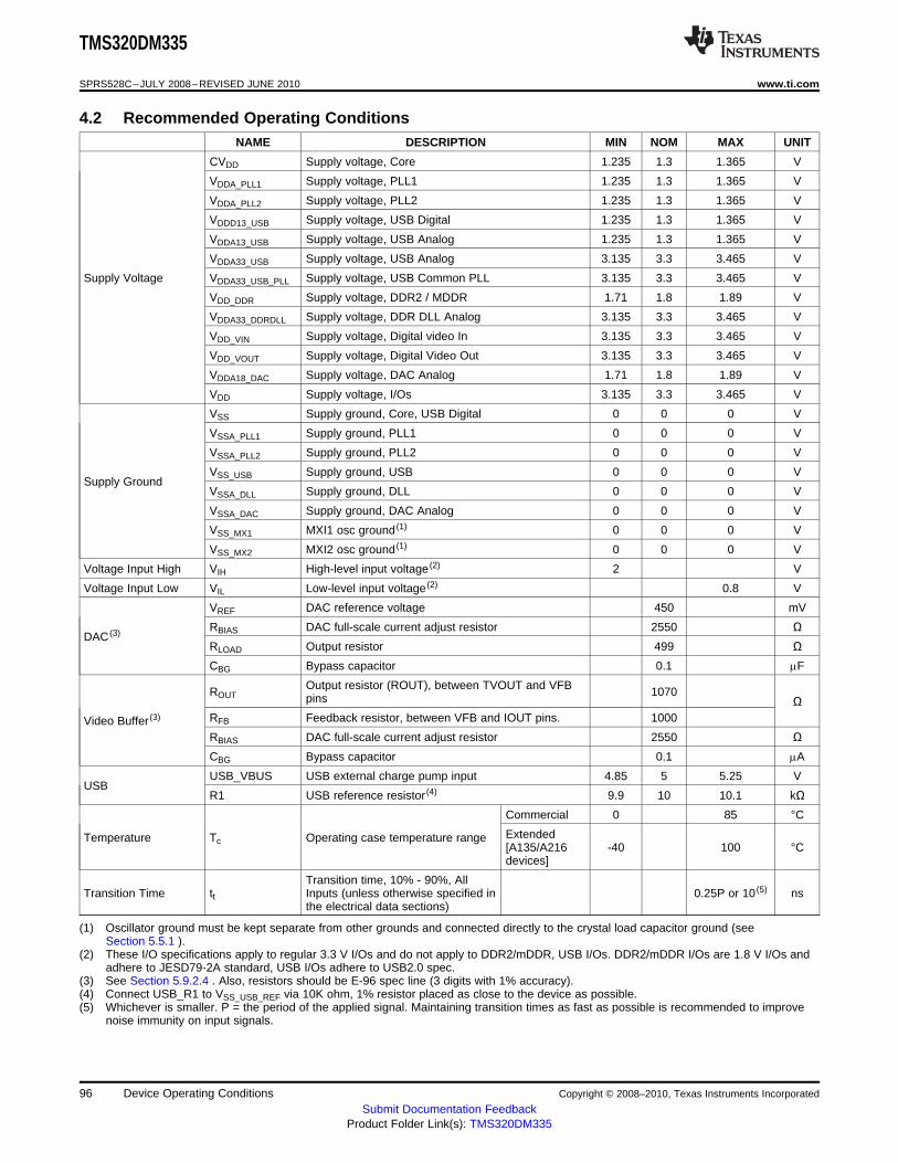
4.1 Absolute Maximum Ratings Over Operating Case2.3 Pin Assignments .................................... 10 Temperature Range2.4 Pin Functions ....................................... 14 (Unless Otherwise Noted) ................................. 952.5 Image Data Output - Video Processing Back End 4.2 Recommended Operating Conditions .............. 96
(VPBE) .............................................. 16 4.3 Electrical Characteristics Over Recommended2.6 Asynchronous External Memory Interface (AEMIF) Ranges of Supply Voltage and Operating Case
...................................................... 19 Temperature (Unless Otherwise Noted) ............ 97
5 DM335 Peripheral Information and Electrical2.7 DDR Memory Interface ............................. 21Specifications .......................................... 98
2.8 GPIO ................................................ 235.1 Parameter Information Device-Specific Information
2.9 Multi-Media Card/Secure Digital (MMC/SD) ...................................................... 98Interfaces ........................................... 28 5.2 Recommended Clock and Control Signal Transition
2.10 Universal Serial Bus (USB) Interface ............... 29 Behavior ............................................ 99
2.11 Audio Interfaces .................................... 30 5.3 Power Supplies ..................................... 99
Revision HistoryNOTE: Page numbers for previous revisions may differ from page numbers in the current version.
This data sheet revision history highlights the technical changes made to the SPRS528B device-specificdata sheet to make it an SPRS528C revision.
Scope: Applicable updates to the DM335 device family, specifically relating to the DM335 device, havebeen incorporated. The A135 and A216 DM335 devices both support extended temperature.
Revision C UpdatesADDS/CHANGES/DELETES
Global Added SPI EEPROM Boot option to NAND.
Section 1.1 Changed Feature bullet from NAND Flash to NAND Flash (with SPI EEPROM Boot option).
Section 2.4 Table 2-9 and Table 2-11:• Added "Used to drive boot status LED signal (active low) in ROM boot modes." to pin number
P16.• Deleted "Used to drive boot status LED signal (active low) in ROM boot modes." from pin
number V19.
Section 2.20 Updated Table 2-23, changed Reset State values.
Section 3.12 Added Section 3.12.2, "RBL NAND Boot Process" and associated Standard and Compatibilitymode references throughout the document.
Section 3.12.1 Added ARM ROM Boot - SPI boot in NAND Mode bullet and sub-bullets.
Figure 3-6 Added SPI Flash to Diagram.
Section 4.2 Added last row to table including table note.
Section 4.3 Updated/Changed the following values in Section 4.3:• IOH MAX value from "-100 mA" to "-4000 mA"• IOZ TYP (IPU disabled) value from "±10 µA" to "±20 µA"• IOZ TYP (IPU enabled) added value of ±100 µA"
Added "Test Conditions" for IOH and IOL parameters
Table 5-5 Changed parameter 4 on table and added table note.
Table 5-6 Changed parameter 4 on table and added table note.
Table 5-45 Changed parameter 4 on table and added table note.
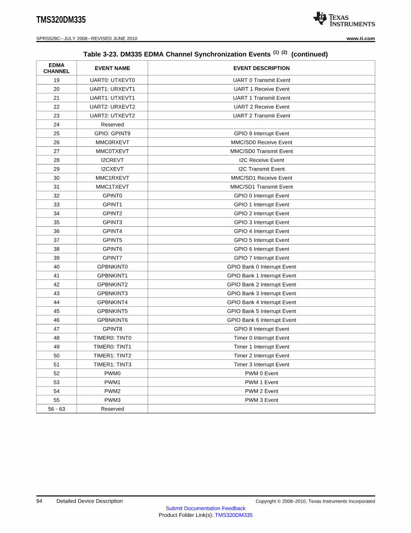
Table 2-1 provides an overview of the DMSoC. The table shows significant features of the device,including the peripherals, capacity of on-chip RAM, ARM operating frequency, the package type with pincount, etc.
Three 64-Bit General Purpose (eachconfigurable as two separate 32-bitTimers timers)Peripherals
One 64-Bit Watch DogNot all peripherals pins are
Three (one with RTS and CTS flowavailable at the same time UART control)(For more detail, see theDevice Configuration Three (each supports two slaveSPIsection). devices)
I2C One (Master/Slave)
Audio Serial Port [ASP] Two ASP
General-Purpose Input/Output Port Up to 104
Pulse width modulator (PWM) Four outputs
One Input (VPFE)Configurable Video Ports One Output (VPBE)
High, Full Speed DeviceUSB 2.0 High, Full, Low Speed Host
ARMOn-Chip CPU Memory Organization 16-KB I-cache, 8-KB D-cache,
Product Preview (PP),Product Status (1) Advance Information (AI), PD
or Production Data (PD)
(1) PRODUCTION DATA information is current as of publication date. Products conform to specifications per the terms of the TexasInstruments standard warranty. Production processing does not necessarily include testing of all parameters.
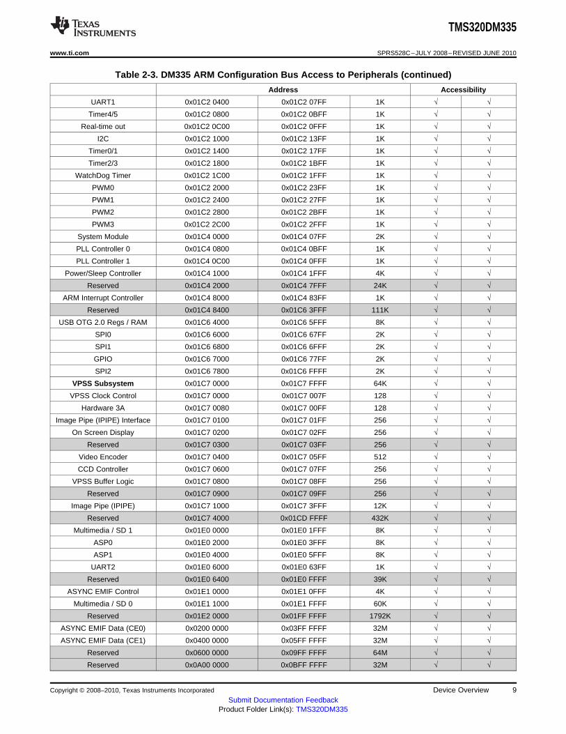
Table 2-3 shows the memory map address ranges of the device. Table 2-3 depicts the expanded map ofthe Configuration Space (0x01C0 0000 through 0x01FF FFFF). The device has multiple on-chip memoriesassociated with its processor and various subsystems. To help simplify software development a unifiedmemory map is used where possible to maintain a consistent view of device resources across all busmasters. The bus masters are the ARM, EDMA, USB, and VPSS.
Table 2-2. DM335 Memory Map
Start Address End Address Size (Bytes) ARM EDMA USB VPSSMem Map Mem Map Mem Map Mem Map
0x0000 0000 0x0000 3FFF 16K ARM RAM0(Instruction)
0x0000 4000 0x0000 7FFF 16K ARM RAM1 Reserved Reserved(Instruction)
0x0000 8000 0x0000 FFFF 32K ARM ROM(Instruction)
- only 8K used
0x0001 0000 0x0001 3FFF 16K ARM RAM0 (Data) ARM RAM0 ARM RAM0
0x0001 4000 0x0001 7FFF 16K ARM RAM1 (Data) ARM RAM1 ARM RAM1
0x0001 8000 0x0001 FFFF 32K ARM ROM (Data) ARM ROM ARM ROM- only 8K used
0x0002 0000 0x000F FFFF 896K Reserved
0x0010 0000 0x01BB FFFF 26M
0x01BC 0000 0x01BC 0FFF 4K ARM ETB Mem
0x01BC 1000 0x01BC 17FF 2K ARM ETB Reg Reserved
0x01BC 1800 0x01BC 18FF 256 ARM IceCrusher Reserved
0x01BC 1900 0x01BC FFFF 59136 Reserved
0x01BD 0000 0x01BF FFFF 192K
0x01C0 0000 0x01FF FFFF 4M CFG Bus CFG Bus ReservedPeripherals Peripherals
Table 2-3. DM335 ARM Configuration Bus Access to Peripherals (continued)
Address Accessibility
Reserved 0x0C00 0000 0x0FFF FFFF 64M √ √
2.3 Pin Assignments
Extensive use of pin multiplexing is used to accommodate the largest number of peripheral functions inthe smallest possible package. Pin multiplexing is controlled using a combination of hardwareconfiguration at device reset and software programmable register settings.
2.3.1 Pin Map (Bottom View)
Figure 2-1 through Figure 2-4 show the pin assignments in four quadrants (A, B, C, and D). Note thatmicro-vias are not required. Contact your TI representative for routing recommendations.
The pin functions tables (Table 2-4 through Table 2-22) identify the external signal names, the associatedpin (ball) numbers along with the mechanical package designator, the pin type, whether the pin has anyinternal pullup or pulldown resistors, and a functional pin description. For more detailed information ondevice configuration, peripheral selection, multiplexed/shared pins, and debugging considerations, seeSection 3. For the list of all pin in chronological order see Section 2.20
2.4.1 Image Data Input - Video Processing Front End
The CCD Controller module in the Video Processing Front End has an external signal interface for imagedata input. It supports YUV (YC) inputs as well as Bayer RGB and complementary input signals (I.e.,image data input).
The definition of the CCD controller data input signals depend on the input mode selected.• In 16-bit YCbCr mode, the Cb and Cr signals are multiplexed on the Cl signals and the order is
configurable (i.e., Cb first or Cr first).• In 8-bit YCbCr mode, the Y, Cb, and Cr signals are multiplexed and not only is the order selectable,
but also the half of the bus used.
Table 2-4. CCD Controller Signals for Each Input Mode
Standard CCD/CMOS input: NOT USED• YCC 16-bit: Time multiplexed between chroma: CB/SR[07]CIN7/ PD • YCC 8-bit (which allows for two simultaneous decoder inputs), it is timeGIO101/ N3 I/O/Z VDD_VIN multiplexed between luma and chroma of the upper channel. Y/CB/CR[07]SPI2_SCLKSPI: SPI2 ClockGIO: GIO[101]
Standard CCD/CMOS input: NOT USED• YCC 16-bit: Time multiplexed between chroma: CB/SR[06]CIN6/ PD • YCC 8-bit (which allows for two simultaneous decoder inputs), it is timeGIO100/ K5 I/O/Z VDD_VIN multiplexed between luma and chroma of the upper channel. Y/CB/CR[06]SPI2_SDOSPI: SPI2 Data OutGIO: GIO[100]
Standard CCD/CMOS input: Raw[13]CIN5/ • YCC 16-bit: Time multiplexed between chroma: CB/SR[05]GIO099/ PD • YCC 8-bit (which allows for two simultaneous decoder inputs), it is timeM3 I/O/ZSPI2_SDEN VDD_VIN multiplexed between luma and chroma of the upper channel. Y/CB/CR[05]A[0] SPI: SPI2 Chip Select
GIO: GIO[099]
Standard CCD/CMOS input: Raw[12]CIN4/ • YCC 16-bit: Time multiplexed between chroma: CB/SR[04]GIO098/ PD • YCC 8-bit (which allows for two simultaneous decoder inputs), it is timeL4 I/O/ZSPI2_SDEN VDD_VIN multiplexed between luma and chroma of the upper channel. Y/CB/CR[04]A[1] SPI: SPI2 Data In
GIO: GIO[098]
Standard CCD/CMOS input(AFE): Raw[11]• YCC 16-bit: Time multiplexed between chroma: CB/SR[03]CIN3/ PDJ4 I/O/Z • YCC 8-bit (which allows for two simultaneous decoder inputs), it is timeGIO097/ VDD_VIN
multiplexed between luma and chroma of the upper channel. Y/CB/CR[03]GIO: GIO[097]
Standard CCD/CMOS input: Raw[10]• YCC 16-bit: Time multiplexed between chroma: CB/SR[02]CIN2/ PDJ5 I/O/Z • YCC 8-bit (which allows for two simultaneous decoder inputs), it is timeGIO096/ VDD_VIN
multiplexed between luma and chroma of the upper channel. Y/CB/CR[02]GIO: GIO[097]
Standard CCD/CMOS input: Raw[09]• YCC 16-bit: Time multiplexed between chroma: CB/SR[01]CIN1/ PDL3 I/O/Z • YCC 8-bit (which allows for two simultaneous decoder inputs), it is timeGIO095/ VDD_VIN
multiplexed between luma and chroma of the upper channel. Y/CB/CR[01]GIO: GIO[095]
Standard CCD/CMOS input: Raw[08]• YCC 16-bit: Time multiplexed between chroma: CB/SR[00]CIN0/ PDJ3 I/O/Z • YCC 8-bit (which allows for two simultaneous decoder inputs), it is timeGIO094/ VDD_VIN
multiplexed between luma and chroma of the upper channel. Y/CB/CR[00]GIO: GIO[094]
Standard CCD/CMOS input: Raw[07]• YCC 16-bit: Time multiplexed between chroma: Y[07]YIN7/ PDL5 I/O/Z • YCC 8-bit (which allows for two simultaneous decoder inputs), it is timeGIO093 VDD_VIN
multiplexed between luma and chroma of the upper channel. Y/CB/CR[07]GIO: GIO[093]
Standard CCD/CMOS input: Raw[06]• YCC 16-bit: Time multiplexed between chroma: Y[06]YIN6/ PDM4 I/O/Z • YCC 8-bit (which allows for two simultaneous decoder inputs), it is timeGIO092 VDD_VIN
multiplexed between luma and chroma of the upper channel. Y/CB/CR[06]GIO: GIO[092]
(1) I = Input, O = Output, Z = High impedance, S = Supply voltage, GND = Ground, A = Analog signal.(2) PD = internal pull-down, PU = internal pull-up. (To pull up a signal to the opposite supply rail, a 1 kΩ resistor should be used.)(3) Specifies the operating I/O supply voltage for each signal. See Section 5.3 , Power Supplies for more detail.
Standard CCD/CMOS input: Raw[05]• YCC 16-bit: Time multiplexed between chroma: Y[05]YIN5/ PDM5 I/O/Z • YCC 8-bit (which allows for two simultaneous decoder inputs), it is timeGIO091 VDD_VIN
multiplexed between luma and chroma of the upper channel. Y/CB/CR[05]GIO: GIO[091]
Standard CCD/CMOS input: Raw[04]• YCC 16-bit: Time multiplexed between chroma: Y[04]YIN4/ PDP3 I/O/Z • YCC 8-bit (which allows for two simultaneous decoder inputs), it is timeGIO090 VDD_VIN
multiplexed between luma and chroma of the upper channel. Y/CB/CR[04]GIO: GIO[090]
Standard CCD/CMOS input: Raw[03]• YCC 16-bit: Time multiplexed between chroma: Y[03]YIN3/ PDR3 I/O/Z • YCC 8-bit (which allows for two simultaneous decoder inputs), it is timeGIO089 VDD_VIN
multiplexed between luma and chroma of the upper channel. Y/CB/CR[03]GIO: GIO[089]
Standard CCD/CMOS input: Raw[02]• YCC 16-bit: Time multiplexed between chroma: Y[02]YIN2/ PDP4 I/O/Z • YCC 8-bit (which allows for two simultaneous decoder inputs), it is timeGIO088 VDD_VIN
multiplexed between luma and chroma of the upper channel. Y/CB/CR[02]GIO: GIO[088]
Standard CCD/CMOS input: Raw[01]• YCC 16-bit: Time multiplexed between chroma: Y[01]YIN1/ PDP2 I/O/Z • YCC 8-bit (which allows for two simultaneous decoder inputs), it is timeGIO087 VDD_VIN
multiplexed between luma and chroma of the upper channel. Y/CB/CR[01]GIO: GIO[087]
Standard CCD/CMOS input: Raw[00]• YCC 16-bit: Time multiplexed between chroma: Y[00]YIN0/ PDP5 I/O/Z • YCC 8-bit (which allows for two simultaneous decoder inputs), it is timeGIO086 VDD_VIN
multiplexed between luma and chroma of the upper channel. Y/CB/CR[00]GIO: GIO[086]
Horizontal synchronization signal that can be either an input (slave mode) or anCAM_HD/ PDN5 I/O/Z output (master mode). Tells the CCDC when a new line starts.GIO085 VDD_VIN GIO: GIO[085]
Vertical synchronization signal that can be either an input (slave mode) or an outputCAM_VD PDR4 I/O/Z (master mode). Tells the CCDC when a new frame starts.GIO084 VDD_VIN GIO: GIO[084]
Write enable input signal is used by external device (AFE/TG) to gate the DDRoutput of the CCDC module. Alternately, the field identification input signal is usedCAM_WEN PD by external device (AFE/TG) to indicate which of two frames is input to the CCDC_FIELD\ R5 I/O/Z VDD_VIN module for sensors with interlaced output. CCDC handles 1- or 2-field sensors inGIO083 hardware.GIO: GIO[083]
PCLK/ PD Pixel clock input (strobe for lines C17 through Y10)T3 I/O/ZGIO082 VDD_VIN GIO: GIO[0082]
2.5 Image Data Output - Video Processing Back End (VPBE)
The Video Encoder/Digital LCD interface module in the video processing back end has an external signalinterface for digital image data output as described in Table 2-7 and Table 2-8.
The digital image data output signals support multiple functions / interfaces, depending on the displaymode selected. The following table describes these modes. Parallel RGB mode with more than RGB565signals requires enabling pin multiplexing to support (i.e., for RGB666 mode).
FIELD / Video Encoder: Field identifier for interlaced display formatsGIO070 / GIO: GIO[070]H4 I/O/Z VDD_VOUTR2 / Digital Video Out: R2PWM3C PWM3C
Video Encoder: External clock input, used if clock rates > 27 MHz are needed, e.g.EXTCLK / 74.25 MHz for HDTV digital outputGIO069 / PDG3 I/O/Z GIO: GIO[069]B2 / VDD_VOUT Digital Video Out: B2PWM3D PWM3D
VCLK / Video Encoder: Video Output ClockH3 I/O/Z VDD_VOUTGIO068 GIO: GIO[068]
(1) I = Input, O = Output, Z = High impedance, S = Supply voltage, GND = Ground, A = Analog signal.(2) Specifies the operating I/O supply voltage for each signal. See Section 5.3 , Power Supplies for more detail.(3) PD = pull-down, PU = pull-up. (To pull up a signal to the opposite supply rail, a 1 kΩ resistor should be used.)(4) To reduce EMI and reflections, depending on the trace length, approximately 22 Ω to 50 Ω damping resistors are recommend on the
following outputs placed near the DM335: YOUT(0-7),COUT(0-7), HSYNC,VSYNC,LCD_OE,FIELD,EXTCLK,VCLK. The trace lengthsshould be minimized.
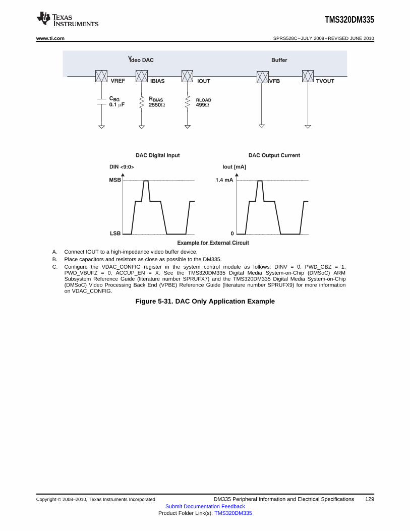
Video DAC: Reference voltage output (0.45V, 0.1uF to GND). When the DAC is notVREF J7 A I/O/Z used, the VREF signal should be connected to VSS.
Video DAC: Pre video buffer DAC output (1000 ohm to VFB). When the DAC is notIOUT E1 A I/O/Z used, the IOUT signal should be connected to VSS.
Video DAC: External resistor (2550 Ohms to GND) connection for current biasIBIAS F2 A I/O/Z configuration. When the DAC is not used, the IBIAS signal should be connected to
VSS.
Video DAC: Pre video buffer DAC output (1000 Ohms to IOUT, 1070 Ohms toVFB G1 A I/O/Z TVOUT). When the DAC is not used, the VFB signal should be connected to VSS.
Video DAC: Analog Composite NTSC/PAL output (SeeFigure 5-31 andFigure 5-32 forTVOUT F1 A I/O/Z V circuit connection). When the DAC is not used, the TVOUT signal should be left as a
No Connect or connected to VSS.
Video DAC: Analog 1.8V power. When the DAC is not used, the VDDA18_DAC signalVDDA18_DAC L7 PWR should be connected to VSS.
Video DAC: Analog 1.8V ground. When the DAC is not used, the VSSA_DAC signalVSSA_DAC L8 GND should be connected to VSS.
(1) I = Input, O = Output, Z = High impedance, S = Supply voltage, GND = Ground, A = Analog signal. Specifies the operating I/O supplyvoltage for each signal. See Section 5.3 , Power Supplies for more detail.
(2) PD = pull-down, PU = pull-up. (To pull up a signal to the opposite supply rail, a 1 kΩ resistor should be used.)
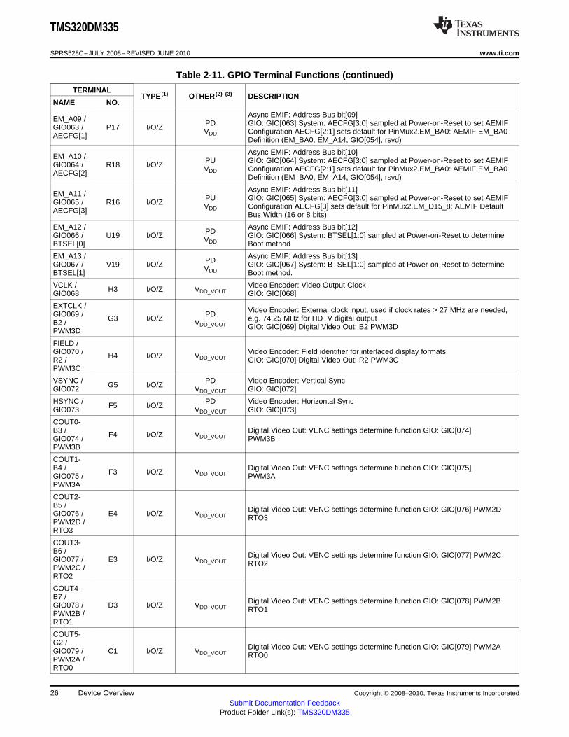
EM_A13/ Async EMIF: Address bus bit[13]PDGIO067/ V19 I/O/Z GIO: GIO[67]VDDBTSEL[1] System: BTSEL[1:0] sampled at power-on-reset to determine boot method.
EM_A12/ Async EMIF: Address bus bit[12]PDGIO066/ U19 I/O/Z GIO: GIO[66]VDDBTSEL[0] System: BTSEL[1:0] sampled at power-on-reset to determine boot method.
Async EMIF: Address bus bit[11]EM_A11/ PU GIO: GIO[65]GIO065/ R16 I/O/Z VDD AECFG[3:0] sampled at power-on-reset to AECFG configuration. AECFG[3] setsAECFG[3] default for PinMux2_EM_D15_8: AEMIF default bus width (16 or 8 bits)
Async EMIF: Address bus bit[10]EM_A10/ GIO: GIO[64]PUGIO064/ R18 I/O/Z AECFG[3:0] sampled at power-on-reset to AECFG configuration. AECFG[2:1]VDDAECFG[2] sets default for PinMux2_EM_BA0: AEMIF EM_BA0 definition (EM_BA0,
EM_A14, GIO[054], rsvd)
Async EMIF: Address bus bit[09]EM_A09/ GIO: GIO[63]PDGIO063/ P17 I/O/Z AECFG[3:0] sampled at power-on-reset to AECFG configuration. AECFG[2:1]VDDAECFG[1] sets default for PinMux2_EM_BA0: AEMIF EM_BA0 definition (EM_BA0,
EM_A14, GIO[054], rsvd)
Async EMIF: Address bus bit[08]GIO: GIO[62]EM_A08/ PD AECFG[0] sets default for:GIO062/ T19 I/O/Z VDDAECFG[0] • PinMux2_EM_A0_BA1: AEMIF address width (OneNAND or NAND)• PinMux2_EM_A13_3: AEMIF address width (OneNAND or NAND)
Async EMIF: Address bus bit[07]EM_A07/ P16 I/O/Z VDD GIO: GIO[61]GIO061 Used to drive boot status LED signal (active low) in ROM boot modes.
(1) I = Input, O = Output, Z = High impedance, S = Supply voltage, GND = Ground, A = Analog signal.(2) Specifies the operating I/O supply voltage for each signal. See Section 5.3 , Power Supplies for more detail.(3) PD = pull-down, PU = pull-up. (To pull up a signal to the opposite supply rail, a 1 kΩ resistor should be used.)
Async EMIF: Address bus bit[01]EM_A01/ N17 I/O/Z VDD NAND/SM/xD: ALE - Address latch enable output
EM_A00/ Async EMIF: Address bus bit[00]M16 I/O/Z VDDGIO056 GIO: GIO[56]
Async EMIF: Bank address 1 signal - 16-bit address:EM_BA1/ • In 16-bit mode, lowest address bit.P19 I/O/Z VDDGIO055 • In 8-bit mode, second lowest address bit.
GIO: GIO[055]
Async EMIF: Bank address 0 signal - 8-bit address:EM_BA0/
• In 8-bit mode, lowest address bit. or can be used as an extra address lineGIO054 N19 I/O/Z VDD (bit14) when using 16-bit memories.EM_A14GIO: GIO[054]
EM_D15/ Async EMIF: Data bus bit 15M18 I/O/Z VDDGIO053 GIO: GIO[053]
EM_D14/ Async EMIF: Data bus bit 14M19 I/O/Z VDDGIO052 GIO: GIO[052]
EM_D13/ Async EMIF: Data bus bit 13M15 I/O/Z VDDGIO051 GIO: GIO[051]
EM_D12/ Async EMIF: Data bus bit 12L18 I/O/Z VDDGIO050 GIO: GIO[050]
EM_D11/ Async EMIF: Data bus bit 11L17 I/O/Z VDDGIO049 GIO: GIO[049]
EM_D10/ Async EMIF: Data bus bit 10L19 I/O/Z VDDGIO048 GIO: GIO[048]
EM_D09/ Async EMIF: Data bus bit 09K18 I/O/Z VDDGIO047 GIO: GIO[047]
EM_D08/ Async EMIF: Data bus bit 08L16 I/O/Z VDDGIO046 GIO: GIO[046]
EM_D07/ Async EMIF: Data bus bit 07K19 I/O/Z VDDGIO045 GIO: GIO[045]
EM_D06/ Async EMIF: Data bus bit 06K17 I/O/Z VDDGIO044 GIO: GIO[044]
EM_D05/ Async EMIF: Data bus bit 05J19 I/O/Z VDDGIO043 GIO: GIO[043]
EM_D04/ Async EMIF: Data bus bit 04L15 I/O/Z VDDGIO042 GIO: GIO[042]
EM_D03/ Async EMIF: Data bus bit 03J18 I/O/Z VDDGIO041 GIO: GIO[041]
EM_D02/ Async EMIF: Data bus bit 02H19 I/O/Z VDDGIO040 GIO: GIO[040]
EM_D01/ Async EMIF: Data bus bit 01J17 I/O/Z VDDGIO039 GIO: GIO[039]
EM_D00/ Async EMIF: Data bus bit 00H18 I/O/Z VDDGIO038 GIO: GIO[038]
Async EMIF: Lowest numbered chip select. Can be programmed to be used forEM_CE0/ standard asynchronous memories (example: flash), OneNAND, or NANDJ16 I/O/Z VDDGIO037 memory. Used for the default boot and ROM boot modes.
GIO: GIO[037]
Async EMIF: Second chip select. Can be programmed to be used for standardEM_CE1/ G19 I/O/Z VDD asynchronous memories(example: flash), OneNAND, or NAND memory.GIO036 GIO: GIO[036]
DDR_DQM[1] U15 I/O/Z VDD_DDR Data mask outputs:• DDR_DQM[1] - For DDR_DQ[15:8]
DDR_DQM[0] T12 I/O/Z VDD_DDR • DDR_DQM[0] - For DDR_DQ[7:0]
DDR_DQS[1] V15 I/O/Z VDD_DDR Data strobe input/outputs for each byte of the 16-bit data bus used tosynchronize the data transfers. Output to DDR when writing and inputs whenreading.
DDR_DQS[0] V12 I/O/Z VDD_DDR • DDR_DQS[1] - For DDR_DQ[15:8]• DDR_DQS[0] - For DDR_DQ[7:0]
DDR_BA[2] V8 I/O/Z VDD_DDR Bank select outputs. Two are required for 1Gb DDR2 memories.
DDR_BA[1] U7 I/O/Z VDD_DDR Bank select outputs. Two are required for 1Gb DDR2 memories.
DDR_BA[0] U8 I/O/Z VDD_DDR Bank select outputs. Two are required for 1Gb DDR2 memories.
DDR_A13 U6 I/O/Z VDD_DDR DDR Address Bus bit 13
DDR_A12 V7 I/O/Z VDD_DDR DDR Address Bus bit 12
DDR_A11 W7 I/O/Z VDD_DDR DDR Address Bus bit 11
DDR_A10 V6 I/O/Z VDD_DDR DDR Address Bus bit 10
(1) I = Input, O = Output, Z = High impedance, S = Supply voltage, GND = Ground, A = Analog signal.(2) Specifies the operating I/O supply voltage for each signal. See Section 5.3 , Power Supplies for more detail.(3) PD = pull-down, PU = pull-up. (To pull up a signal to the opposite supply rail, a 1 kΩ resistor should be used.)
DDR_ DDR: Loopback signal for external DQS gating. Route to DDR and back toW18 I/O/Z VDD_DDRDQGATE0 DDR_DQGATE1 with same constraints as used for DDR clock and data.
DDR_ DDR: Loopback signal for external DQS gating. Route to DDR and back toV17 I/O/Z VDD_DDRDQGATE1 DDR_DQGATE0 with same constraints as used for DDR clock and data.
DDR: Voltage input for the SSTL_18 I/O buffers. Note even in the case ofDDR_VREF U10 I/O/Z VDD_DDR mDDR an external resistor divider connected to this pin is necessary.
VSSA_DLL R11 I/O/Z VDD_DDR DDR: Ground for the DDR DLL
VDDA33_DDRDL R10 I/O/Z VDD_DDR DDR: Power (3.3 V) for the DDR DLLL
DDR: Reference output for drive strength calibration of N and P channelDDR_ZN T9 I/O/Z VDD_DDR outputs. Tie to ground via 50 ohm resistor @ 0.5% tolerance.
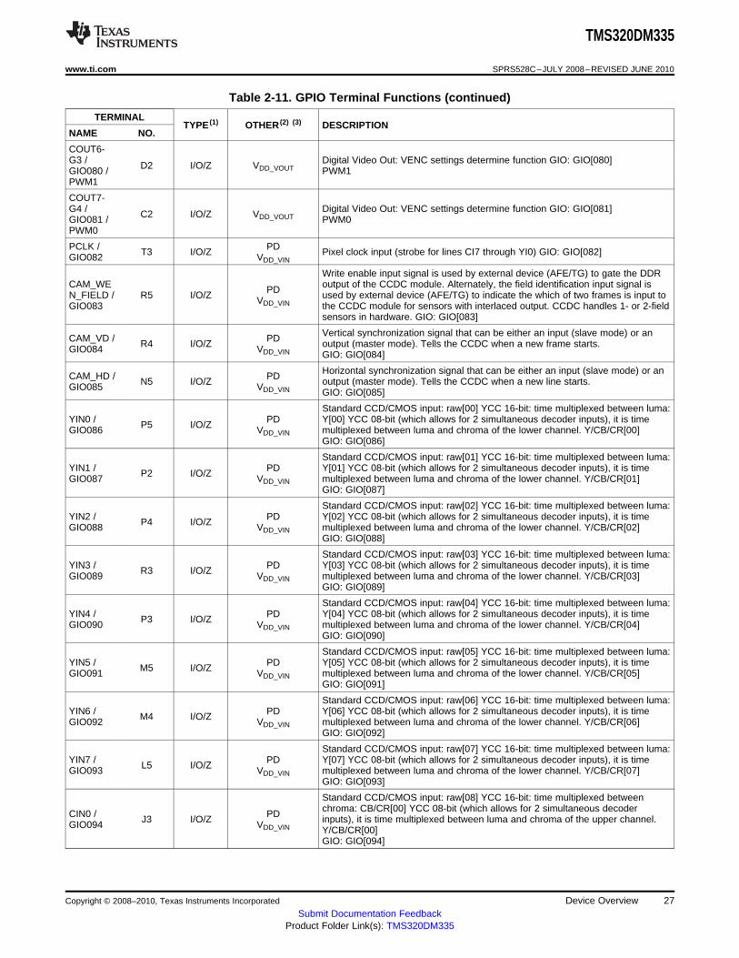
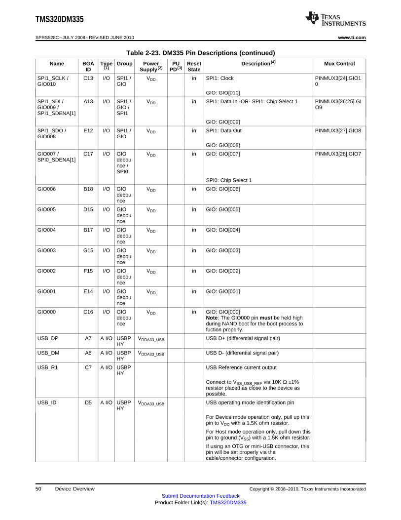
The General Purpose I/O signals provide generic I/O to external devices. Most of the GIO signals aremultiplexed with other functions.
Table 2-11. GPIO Terminal Functions
TERMINALTYPE (1) OTHER (2) (3) DESCRIPTION
NAME NO.
GIO:GIO[000] is sampled at reset and stored in the GIO0_RESET bit of theBOOTCFG register.Active low during MMC/SD boot (can be used as MMC/SD power control).GIO000 C16 I/O/Z VDD Can be used as external clock input for Timer 3.Note: The GIO000 pin must be held high during NAND boot for the bootprocess to fuction properly.
GIO001 E14 I/O/Z VDD GIO: GIO[001] Can be used as external clock input for Timer 3.
GIO002 F15 I/O/Z VDD GIO: GIO[002] Can be used as external clock input for Timer 3.
GIO003 G15 I/O/Z VDD GIO: GIO[003] Can be used as external clock input for Timer 3.
(1) I = Input, O = Output, Z = High impedance, S = Supply voltage, GND = Ground, A = Analog signal.(2) Specifies the operating I/O supply voltage for each signal. See Section 5.3 , Power Supplies for more detail.(3) PD = pull-down, PU = pull-up. (To pull up a signal to the opposite supply rail, a 1 kΩ resistor should be used.)
Async EMIF: Second Chip Select., Can be programmed to be used for standardEM_CE1 / G19 I/O/Z VDD asynchronous memories (example: flash), OneNand or NAND memory.GIO036 GIO: GIO[036]
Async EMIF: Lowest numbered Chip Select. Can be programmed to be used forEM_CE0 / standard asynchronous memories (example: flash), OneNand or NAND memory.J16 I/O/Z VDDGIO037 Used for the default boot and ROM boot modes.
GIO: GIO[037]
EM_D00 / Async EMIF: Data Bus bit[00]H18 I/O/Z VDDGIO038 GIO: GIO[038]
EM_D01 / Async EMIF: Data Bus bit[01]J17 I/O/Z VDDGIO039 GIO: GIO[039]
EM_D02 / Async EMIF: Data Bus bit[02]H19 I/O/Z VDDGIO040 GIO: GIO[040]
EM_D03 / Async EMIF: Data Bus bit[03]J18 I/O/Z VDDGIO041 GIO: GIO[041]
EM_D04 / Async EMIF: Data Bus bit[04]L15 I/O/Z VDDGIO042 GIO: GIO[042]
EM_D05 / Async EMIF: Data Bus bit[05]J19 I/O/Z VDDGIO043 GIO: GIO[043]
EM_D06 / Async EMIF: Data Bus bit[06]K17 I/O/Z VDDGIO044 GIO: GIO[044]
EM_D07 / Async EMIF: Data Bus bit[07]K19 I/O/Z VDDGIO045 GIO: GIO[045]
EM_D08 / Async EMIF: Data Bus bit[08]L16 I/O/Z VDDGIO046 GIO: GIO[046]
EM_D09 / Async EMIF: Data Bus bit[09]K18 I/O/Z VDDGIO047 GIO: GIO[047]
EM_D10 / Async EMIF: Data Bus bit[10]L19 I/O/Z VDDGIO048 GIO: GIO[048]
EM_D11 / Async EMIF: Data Bus bit[11]L17 I/O/Z VDDGIO049 GIO: GIO[049]
EM_D12 / Async EMIF: Data Bus bit[12]L18 I/O/Z VDDGIO050 GIO: GIO[050]
EM_D13 / Async EMIF: Data Bus bit[13]M15 I/O/Z VDDGIO051 GIO: GIO[051]
EM_D14 / Async EMIF: Data Bus bit[14]M19 I/O/Z VDDGIO052 GIO: GIO[052]
EM_D15 / Async EMIF: Data Bus bit[15]M18 I/O/Z VDDGIO053 GIO: GIO[053]
Async EMIF: Bank Address 0 signal = 8-bit address. In 8-bit mode, lowestEM_BA0 / address bit. Or, can be used as an extra Address line (bit[14] when using 16-bitGIO054 / N19 I/O/Z VDD memories.EM_A14 GIO: GIO[054]
Async EMIF: Bank Address 1 signal = 16-bit address. In 16-bit mode, lowestEM_BA1 / P19 I/O/Z VDD address bit. In 8-bit mode, second lowest address bitGIO055 GIO: GIO[055]
Async EMIF: Address Bus bit[00] Note that the EM_A0 is always a 32-bitEM_A00 / M16 I/O/Z VDD addressGIO056 GIO: GIO[056]
Async EMIF: Address Bus bit[09]EM_A09 / PD GIO: GIO[063] System: AECFG[3:0] sampled at Power-on-Reset to set AEMIFGIO063 / P17 I/O/Z VDD Configuration AECFG[2:1] sets default for PinMux2.EM_BA0: AEMIF EM_BA0AECFG[1] Definition (EM_BA0, EM_A14, GIO[054], rsvd)
Async EMIF: Address Bus bit[10]EM_A10 / PU GIO: GIO[064] System: AECFG[3:0] sampled at Power-on-Reset to set AEMIFGIO064 / R18 I/O/Z VDD Configuration AECFG[2:1] sets default for PinMux2.EM_BA0: AEMIF EM_BA0AECFG[2] Definition (EM_BA0, EM_A14, GIO[054], rsvd)
Async EMIF: Address Bus bit[11]EM_A11 / PU GIO: GIO[065] System: AECFG[3:0] sampled at Power-on-Reset to set AEMIFGIO065 / R16 I/O/Z VDD Configuration AECFG[3] sets default for PinMux2.EM_D15_8: AEMIF DefaultAECFG[3] Bus Width (16 or 8 bits)
EM_A12 / Async EMIF: Address Bus bit[12]PDGIO066 / U19 I/O/Z GIO: GIO[066] System: BTSEL[1:0] sampled at Power-on-Reset to determineVDDBTSEL[0] Boot method
EM_A13 / Async EMIF: Address Bus bit[13]PDGIO067 / V19 I/O/Z GIO: GIO[067] System: BTSEL[1:0] sampled at Power-on-Reset to determineVDDBTSEL[1] Boot method.
VCLK / Video Encoder: Video Output ClockH3 I/O/Z VDD_VOUTGIO068 GIO: GIO[068]
EXTCLK / Video Encoder: External clock input, used if clock rates > 27 MHz are needed,GIO069 / PDG3 I/O/Z e.g. 74.25 MHz for HDTV digital outputB2 / VDD_VOUT GIO: GIO[069] Digital Video Out: B2 PWM3DPWM3D
FIELD /GIO070 / Video Encoder: Field identifier for interlaced display formatsH4 I/O/Z VDD_VOUTR2 / GIO: GIO[070] Digital Video Out: R2 PWM3CPWM3C
COUT6-G3 / Digital Video Out: VENC settings determine function GIO: GIO[080]D2 I/O/Z VDD_VOUTGIO080 / PWM1PWM1
COUT7-G4 / Digital Video Out: VENC settings determine function GIO: GIO[081]C2 I/O/Z VDD_VOUTGIO081 / PWM0PWM0
PCLK / PDT3 I/O/Z Pixel clock input (strobe for lines CI7 through YI0) GIO: GIO[082]GIO082 VDD_VIN
Write enable input signal is used by external device (AFE/TG) to gate the DDRCAM_WE output of the CCDC module. Alternately, the field identification input signal isPDN_FIELD / R5 I/O/Z used by external device (AFE/TG) to indicate the which of two frames is input toVDD_VINGIO083 the CCDC module for sensors with interlaced output. CCDC handles 1- or 2-field
sensors in hardware. GIO: GIO[083]
Vertical synchronization signal that can be either an input (slave mode) or anCAM_VD / PDR4 I/O/Z output (master mode). Tells the CCDC when a new frame starts.GIO084 VDD_VIN GIO: GIO[084]
Horizontal synchronization signal that can be either an input (slave mode) or anCAM_HD / PDN5 I/O/Z output (master mode). Tells the CCDC when a new line starts.GIO085 VDD_VIN GIO: GIO[085]
Standard CCD/CMOS input: raw[00] YCC 16-bit: time multiplexed between luma:YIN0 / PD Y[00] YCC 08-bit (which allows for 2 simultaneous decoder inputs), it is timeP5 I/O/ZGIO086 VDD_VIN multiplexed between luma and chroma of the lower channel. Y/CB/CR[00]
GIO: GIO[086]
Standard CCD/CMOS input: raw[01] YCC 16-bit: time multiplexed between luma:YIN1 / PD Y[01] YCC 08-bit (which allows for 2 simultaneous decoder inputs), it is timeP2 I/O/ZGIO087 VDD_VIN multiplexed between luma and chroma of the lower channel. Y/CB/CR[01]
GIO: GIO[087]
Standard CCD/CMOS input: raw[02] YCC 16-bit: time multiplexed between luma:YIN2 / PD Y[02] YCC 08-bit (which allows for 2 simultaneous decoder inputs), it is timeP4 I/O/ZGIO088 VDD_VIN multiplexed between luma and chroma of the lower channel. Y/CB/CR[02]
GIO: GIO[088]
Standard CCD/CMOS input: raw[03] YCC 16-bit: time multiplexed between luma:YIN3 / PD Y[03] YCC 08-bit (which allows for 2 simultaneous decoder inputs), it is timeR3 I/O/ZGIO089 VDD_VIN multiplexed between luma and chroma of the lower channel. Y/CB/CR[03]
GIO: GIO[089]
Standard CCD/CMOS input: raw[04] YCC 16-bit: time multiplexed between luma:YIN4 / PD Y[04] YCC 08-bit (which allows for 2 simultaneous decoder inputs), it is timeP3 I/O/ZGIO090 VDD_VIN multiplexed between luma and chroma of the lower channel. Y/CB/CR[04]
GIO: GIO[090]
Standard CCD/CMOS input: raw[05] YCC 16-bit: time multiplexed between luma:YIN5 / PD Y[05] YCC 08-bit (which allows for 2 simultaneous decoder inputs), it is timeM5 I/O/ZGIO091 VDD_VIN multiplexed between luma and chroma of the lower channel. Y/CB/CR[05]
GIO: GIO[091]
Standard CCD/CMOS input: raw[06] YCC 16-bit: time multiplexed between luma:YIN6 / PD Y[06] YCC 08-bit (which allows for 2 simultaneous decoder inputs), it is timeM4 I/O/ZGIO092 VDD_VIN multiplexed between luma and chroma of the lower channel. Y/CB/CR[06]
GIO: GIO[092]
Standard CCD/CMOS input: raw[07] YCC 16-bit: time multiplexed between luma:YIN7 / PD Y[07] YCC 08-bit (which allows for 2 simultaneous decoder inputs), it is timeL5 I/O/ZGIO093 VDD_VIN multiplexed between luma and chroma of the lower channel. Y/CB/CR[07]
GIO: GIO[093]
Standard CCD/CMOS input: raw[08] YCC 16-bit: time multiplexed betweenchroma: CB/CR[00] YCC 08-bit (which allows for 2 simultaneous decoderCIN0 / PDJ3 I/O/Z inputs), it is time multiplexed between luma and chroma of the upper channel.GIO094 VDD_VIN Y/CB/CR[00]GIO: GIO[094]
Standard CCD/CMOS input: raw[09] YCC 16-bit: time multiplexed betweenchroma: CB/CR[01] YCC 08-bit (which allows for 2 simultaneous decoderCIN1 / PDL3 I/O/Z inputs), it is time multiplexed between luma and chroma of the upper channel.GIO095 VDD_VIN Y/CB/CR[01]GIO: GIO[095]
Standard CCD/CMOS input: raw[10] YCC 16-bit: time multiplexed betweenchroma: CB/CR[02] YCC 08-bit (which allows for 2 simultaneous decoderCIN2 / PDJ5 I/O/Z inputs), it is time multiplexed between luma and chroma of the upper channel.GIO096 VDD_VIN Y/CB/CR[02]GIO: GIO[096]
Standard CCD/CMOS input: raw[11] YCC 16-bit: time multiplexed betweenchroma: CB/CR[03] YCC 08-bit (which allows for 2 simultaneous decoderCIN3 / PDJ4 I/O/Z inputs), it is time multiplexed between luma and chroma of the upper channel.GIO097 VDD_VIN Y/CB/CR[03]GIO: GIO[097]
CIN4 / Standard CCD/CMOS input: raw[12] YCC 16-bit: time multiplexed betweenGIO098 / chroma: CB/CR[04] YCC 08-bit (which allows for 2 simultaneous decoderSPI2_SDI PDL4 I/O/Z inputs), it is time multiplexed between luma and chroma of the upper channel./ VDD_VIN Y/CB/CR[04] SPI: SPI2 Data In -OR- SPI2 Chip select 1.SPI2_SDE GIO: GIO[098]NA[1]
Standard CCD/CMOS input: raw[13] YCC 16-bit: time multiplexed betweenCIN5 / chroma: CB/CR[05] YCC 08-bit (which allows for 2 simultaneous decoderGIO099 / PDM3 I/O/Z inputs), it is time multiplexed between luma and chroma of the upper channel.SPI2_SDE VDD_VIN Y/CB/CR[05] SPI: SPI2 Chip Select 0.NA[0] GIO: GIO[99]
Standard CCD/CMOS input: NOT USED YCC 16-bit: time multiplexed betweenCIN6 / chroma: CB/CR[06] YCC 08-bit (which allows for 2 simultaneous decoderGIO100 / PDK5 I/O/Z inputs), it is time multiplexed between luma and chroma of the upper channel.SPI2_SD VDD_VIN Y/CB/CR[06] SPI: SPI2 Data OutO GIO: GIO[100]
Standard CCD/CMOS input: NOT USED YCC 16-bit: time multiplexed betweenCIN7 / chroma: CB/CR[07] YCC 08-bit (which allows for 2 simultaneous decoderGIO101 / PDN3 I/O/Z inputs), it is time multiplexed between luma and chroma of the upper channel.SPI2_SCL VDD_VIN Y/CB/CR[07] SPI: SPI2 ClockK GIO: GIO[101]
SPI0_SDI SPI0: Data InA12 I/O/Z VDD/ GIO102 GIO: GIO[102]
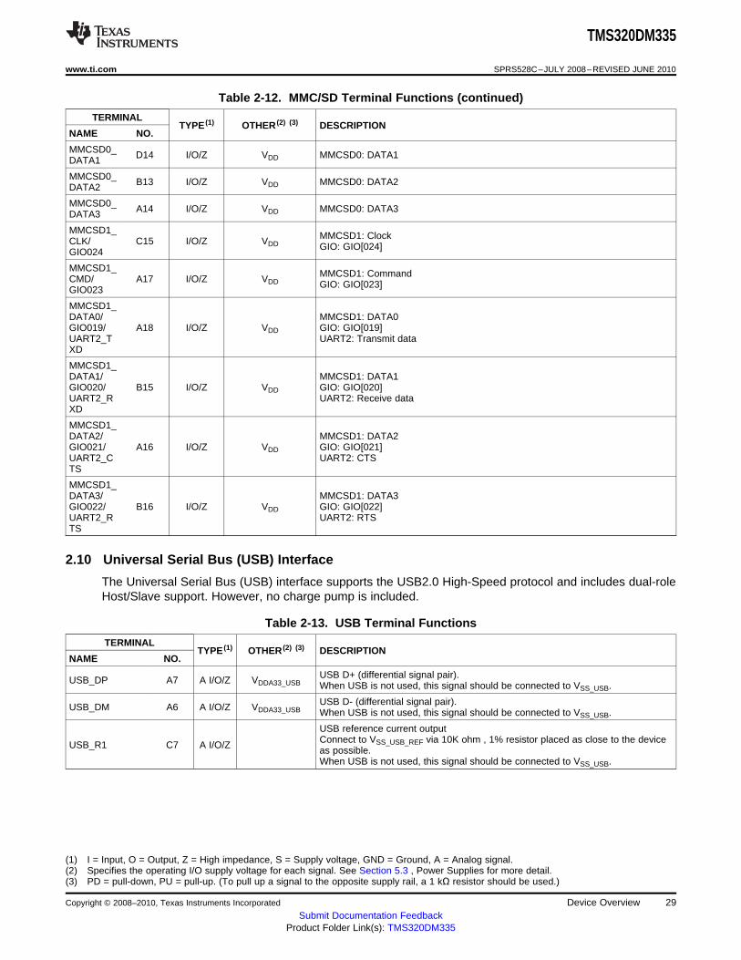
2.9 Multi-Media Card/Secure Digital (MMC/SD) Interfaces
The DM335 includes two Multi-Media Card/Secure Digital card interfaces that are compatible with theMMC/SD and SDIO protocol.
Table 2-12. MMC/SD Terminal Functions
TERMINALTYPE (1) OTHER (2) (3) DESCRIPTION
NAME NO.
MMCSD0_ A15 I/O/Z VDD MMCSD0: ClockCLK
MMCSD0_ C14 I/O/Z VDD MMCSD0: CommandCMD
MMCSD0_ B14 I/O/Z VDD MMCSD0: DATA0DATA0
(1) I = Input, O = Output, Z = High impedance, S = Supply voltage, GND = Ground, A = Analog signal.(2) Specifies the operating I/O supply voltage for each signal. See Section 5.3 , Power Supplies for more detail.(3) PD = pull-down, PU = pull-up. (To pull up a signal to the opposite supply rail, a 1 kΩ resistor should be used.)
The Universal Serial Bus (USB) interface supports the USB2.0 High-Speed protocol and includes dual-roleHost/Slave support. However, no charge pump is included.
Table 2-13. USB Terminal Functions
TERMINALTYPE (1) OTHER (2) (3) DESCRIPTION
NAME NO.
USB D+ (differential signal pair).USB_DP A7 A I/O/Z VDDA33_USB When USB is not used, this signal should be connected to VSS_USB.
USB D- (differential signal pair).USB_DM A6 A I/O/Z VDDA33_USB When USB is not used, this signal should be connected to VSS_USB.
USB reference current outputConnect to VSS_USB_REF via 10K ohm , 1% resistor placed as close to the deviceUSB_R1 C7 A I/O/Z as possible.When USB is not used, this signal should be connected to VSS_USB.
(1) I = Input, O = Output, Z = High impedance, S = Supply voltage, GND = Ground, A = Analog signal.(2) Specifies the operating I/O supply voltage for each signal. See Section 5.3 , Power Supplies for more detail.(3) PD = pull-down, PU = pull-up. (To pull up a signal to the opposite supply rail, a 1 kΩ resistor should be used.)
USB operating mode identification pinFor Device mode operation only, pull up this pin to VDD with a 1.5K ohm resistor.For Host mode operation only, pull down this pin to ground (VSS) with a 1.5K ohm
USB_ID D5 A I/O/Z VDDA33_USB resistor.If using an OTG or mini-USB connector, this pin will be set properly via thecable/connector configuration.When USB is not used, this signal should be connected to VSS_USB.
For host or device mode operation, tie the VBUS/USB power signal to the USBconnector.
USB_VBUS E5 A I/O/Z VDD When used in OTG mode operation, tie VBUS to the external charge pump andto the VBUS signal on the USB connector.When the USB is not used, tie VBUS to VSS_USB.
Digital output to control external 5 V supplyUSB_DRVVBUS C5 O/Z VDD When USB is not used, this signal should be left as a No Connect.
USB Ground ReferenceVSS_USB_REF C8 GND VDD Connect directly to ground and to USB_R1 via 10K ohm, 1% resistor placed as
close to the device as possible.
Analog 3.3 V power USBPHYVDDA33_USB J8 PWR VDD When USB is not used, this signal should be connected to VSS_USB.
Common mode 3.3 V power for USB PHY (PLL)VDDA33_USB_PLL B6 PWR VDD When USB is not used, this signal should be connected to VSS_USB.
Analog 1.3 V power for USB PHYVDDA13_USB H7 PWR VDD When USB is not used, this signal should be connected to VSS_USB.
Digital 1.3 V power for USB PHYVDDD13_USB C6 PWR VDD When USB is not used, this signal should be connected to VSS_USB.
2.11 Audio Interfaces
The DM335 includes two Audio Serial Ports (ASP ports), which are backward compatible with other TIASP serial ports and provide I2S audio interface. One interface is multiplexed with GIO signals.
(1) I = Input, O = Output, Z = High impedance, S = Supply voltage, GND = Ground, A = Analog signal.(2) Specifies the operating I/O supply voltage for each signal. See Section 5.3 , Power Supplies for more detail.(3) PD = pull-down, PU = pull-up. (To pull up a signal to the opposite supply rail, a 1 kΩ resistor should be used.)
(1) I = Input, O = Output, Z = High impedance, S = Supply voltage, GND = Ground, A = Analog signal.(2) Specifies the operating I/O supply voltage for each signal. See Section 5.3 , Power Supplies for more detail.(3) PD = pull-down, PU = pull-up. (To pull up a signal to the opposite supply rail, a 1 kΩ resistor should be used.)
The DM335 includes an I2C two-wire serial interface for control of external peripherals. This interface ismultiplexed with GIO signals.
Table 2-16. I2C Terminal Functions
TERMINALTYPE (1) OTHER (2) (3) DESCRIPTION
NAME NO.
I2C_SDA/ I2C: Serial dataR13 I/O/Z VDDGIO015 GIO: GIO015
I2C_SCL/ I2C: Serial clockR14 I/O/Z VDDGIO014 GIO: GIO014
(1) I = Input, O = Output, Z = High impedance, S = Supply voltage, GND = Ground, A = Analog signal.(2) Specifies the operating I/O supply voltage for each signal. See Section 5.3 , Power Supplies for more detail.(3) PD = pull-down, PU = pull-up. (To pull up a signal to the opposite supply rail, a 1 kΩ resistor should be used.)
2.14 Serial Interface
The DM335 includes three independent serial ports. These interfaces are multiplexed with GIO and othersignals.
SPI1: Chip select 0SPI1_SDENA[0]/ E13 I/O/Z VDD GIO: GIO[011] - Active low during MMC/SD boot (can be used asGIO011 MMC/SD power control)
SPI1_SDI/ SPI1: Data in orGIO009/ A13 I/O/Z VDD SPI1: Chip select 1SPI1_SDENA[1] GIO: GIO[09]
SPI1_SDO/ SPI1: Data outE12 I/O/Z VDDGIO008 GIO: GIO[008]
Standard CCD/CMOS input: Not used• YCC 16-bit: time multiplexed between chroma. CB/CR[07]
CIN7/ • YCC 8-bit (which allows for two simultaneous decoder inputs), it isPDGIO101/ N3 I/O/Z time multiplexed between luma and chroma of the upper channel.VDD_VINSPI2_SCLK Y/CB/CR[07]SPI: SPI2 clockGIO: GIO[101]
Standard CCD/CMOS input: Raw[13]• YCC 16-bit: time multiplexed between chroma. CB/CR[05]
CIN5/ • YCC 8-bit (which allows for two simultaneous decoder inputs), it isPDGIO099/ M3 I/O/Z time multiplexed between luma and chroma of the upper channel.VDD_VINSPI2_SDENA[0] Y/CB/CR[07]SPI: SPI2 chip select 0GIO: GIO[099]
(1) I = Input, O = Output, Z = High impedance, S = Supply voltage, GND = Ground, A = Analog signal.(2) Specifies the operating I/O supply voltage for each signal. See Section 5.3 , Power Supplies for more detail.(3) PD = pull-down, PU = pull-up. (To pull up a signal to the opposite supply rail, a 1 kΩ resistor should be used.)
Standard CCD/CMOS input: Raw[12]• YCC 16-bit: time multiplexed between chroma. CB/CR[04]CIN4/• YCC 8-bit (which allows for two simultaneous decoder inputs), it isGIO098/ PDL4 I/O/Z time multiplexed between luma and chroma of the upper channel.SPI2_SDI/ VDD_VIN
Y/CB/CR[04]SPI2_SDENA[1]SPI: SPI2 Data in -OR- SPI2 Chip select 1GIO: GIO[0998]
Standard CCD/CMOS input: Not used• YCC 16-bit: time multiplexed between chroma. CB/CR[06]
CIN6/ • YCC 8-bit (which allows for two simultaneous decoder inputs), it isPDGIO100/ K5 I/O/Z time multiplexed between luma and chroma of the upper channel.VDD_VINSPI2_SDO/ Y/CB/CR[06]SPI: SPI2 Data outGIO: GIO[100]
2.15 Clock Interface
The DM335 provides interface with the system clocks.
MXI1 A9 I VDD Crystal input for system oscillator (24 MHz or 36 MHz)
Output for system oscillator (24 MHz or 36 MHz). When the MX02 is not used,MXO1 B9 O VDD the MX02 signal can be left open.
Crystal input for video oscillator (27 MHz) Optional, use only if 27MHz derivedfrom MXI1 and PLL does not provide sufficient performance for Video DAC.MXI2 R1 I VDD When the MXI2 is not used and powered down, the MXI2 signal should be leftas a No Connect
Output for video oscillator (27 MHz) Optional, use only if 27MHz derived fromMXI1 and PLL does not provide sufficient performance for Video DAC When theMXO2 T1 O VDD MXO2 is not used and powered down, the MXO2 signal should be left as a NoConnect.
(1) I = Input, O = Output, Z = High impedance, S = Supply voltage, GND = Ground, A = Analog signal.(2) Specifies the operating I/O supply voltage for each signal. See Section 5.3 , Power Supplies for more detail.(3) PD = pull-down, PU = pull-up. (To pull up a signal to the opposite supply rail, a 1 kΩ resistor should be used.)
The DM335 provides Real Time Output (RTO) interface.
Table 2-19. RTO Terminal Functions
TERMINALTYPE (1) OTHER (2) (3) DESCRIPTION
NAME NO.
COUT5-G2 / Digital Video Out: VENC settings determine function GIO: GIO[079]GIO079 / C1 I/O/Z VDD_VOUT PWM2APWM2A / RTO0RTO0
COUT4-B7 / Digital Video Out: VENC settings determine function GIO: GIO[078]GIO078 / D3 I/O/Z VDD_VOUT PWM2BPWM2B / RTO1RTO1
COUT3-B6 / Digital Video Out: VENC settings determine function GIO: GIO[077]GIO077 / E3 I/O/Z VDD_VOUT PWM2CPWM2C / RTO2RTO2
COUT2-B5 / Digital Video Out: VENC settings determine function GIO: GIO[076]GIO076 / E4 I/O/Z VDD_VOUT PWM2DPWM2D / RTO3RTO3
(1) I = Input, O = Output, Z = High impedance, S = Supply voltage, GND = Ground, A = Analog signal.(2) Specifies the operating I/O supply voltage for each signal. See Section 5.3 , Power Supplies for more detail.(3) PD = pull-down, PU = pull-up. (To pull up a signal to the opposite supply rail, a 1 kΩ resistor should be used.)
2.17 Pulse Width Modulator (PWM) Interface
The DM335 provides Pulse Width Modulator (PWM) interface.
Table 2-20. PWM Terminal Functions
TERMINALTYPE (1) OTHER (2) (3) DESCRIPTION
NAME NO.
COUT7-G4 / Digital Video Out: VENC settings determine function GIO: GIO[081]C2 I/O/Z VDD_VOUTGIO081 / PWM0PWM0
COUT6-G3 / Digital Video Out: VENC settings determine function GIO: GIO[080]D2 I/O/Z VDD_VOUTGIO080 / PWM1PWM1
COUT5-G2 / Digital Video Out: VENC settings determine function GIO: GIO[079]GIO079 / C1 I/O/Z VDD_VOUT PWM2APWM2A / RTO0RTO0
COUT4-B7 / Digital Video Out: VENC settings determine function GIO: GIO[078]GIO078 / D3 I/O/Z VDD_VOUT PWM2BPWM2B / RTO1RTO1
(1) I = Input, O = Output, Z = High impedance, S = Supply voltage, GND = Ground, A = Analog signal.(2) Specifies the operating I/O supply voltage for each signal. See Section 5.3 , Power Supplies for more detail.(3) PD = pull-down, PU = pull-up. (To pull up a signal to the opposite supply rail, a 1 kΩ resistor should be used.)
COUT3-B6 / Digital Video Out: VENC settings determine function GIO: GIO[077]GIO077 / E3 I/O/Z VDD_VOUT PWM2CPWM2C / RTO2RTO2
COUT2-B5 / Digital Video Out: VENC settings determine function GIO: GIO[076]GIO076 / E4 I/O/Z VDD_VOUT PWM2DPWM2D / RTO3RTO3
COUT1-B4 / Digital Video Out: VENC settings determine function GIO: GIO[075]F3 I/O/Z VDD_VOUTGIO075 / PWM3APWM3A
COUT0-B3 / Digital Video Out: VENC settings determine function GIO: GIO[074]F4 I/O/Z VDD_VOUTGIO074 / PWM3BPWM3B
FIELD / Video Encoder: Field identifier for interlaced display formats GIO: GIO[070]GIO070 / H4 I/O/Z VDD_VOUT Digital Video Out: R2R2 / PWM3CPWM3C
EXTCLK / Video Encoder: External clock input, used if clock rates > 27 MHz are needed,GIO069 / PDG3 I/O/Z e.g. 74.25 MHz for HDTV digital output GIO: GIO[069] Digital Video Out: B2B2 / VDD_VOUT PWM3DPWM3D
2.18 System Configuration Interface
The DM335 provides interfaces for system configuration and boot load.
Table 2-21. System/Boot Terminal Functions
TERMINALTYPE (1) OTHER (2) (3) DESCRIPTION
NAME NO.
EM_A13/ Async EMIF: Address bus bit 13PDGIO067/ V19 I/O/Z GIO: GIO[067]VDDBTSEL[1] System: BTSEL[1:0] sampled at power-on-reset to determine boot method.
EM_A12/ Async EMIF: Address bus bit 12PDGIO066/ U19 I/O/Z GIO: GIO[066]VDDBTSEL[0] System: BTSEL[1:0] sampled at power-on-reset to determine boot method.
Async EMIF: Address bus bit 11EM_A11/ GIO: GIO[065]PUGIO065/ R16 I/O/Z System: AECFG[3:0] sampled a power-on-reset to set AEMIF configuration.VDDAECFG[3] AECFG[3] sets default fo PinMux2.EM_D15_8. AEMIF default bus width (16 or 8
bits).
Async EMIF: Address bus bit 10EM_A10/ GIO: GIO[064]PUGIO064/ R18 I/O/Z System: AECFG[3:0] sampled a power-on-reset to set AEMIF configuration.VDDAECFG[2] AECFG[2:1] sets default fo PinMux2.EM_BA0. AEMIF EM_BA0 definition:
(EM,_BA0, EM_A14, GIO[054], rsvd)
Async EMIF: Address bus bit 09EM_A09/ GIO: GIO[063]PDGIO063/ P17 I/O/Z System: AECFG[3:0] sampled a power-on-reset to set AEMIF configuration.VDDAECFG[1] AECFG[2:1] sets default fo PinMux2.EM_BA0. AEMIF EM_BA0 definition:
(EM,_BA0, EM_A14, GIO[054], rsvd)
(1) I = Input, O = Output, Z = High impedance, S = Supply voltage, GND = Ground, A = Analog signal.(2) Specifies the operating I/O supply voltage for each signal. See Section 5.3 , Power Supplies for more detail.(3) PD = pull-down, PU = pull-up. (To pull up a signal to the opposite supply rail, a 1 kΩ resistor should be used.)
Async EMIF: Address bus bit 08GIO: GIO[062]EM_A08/ PD System: AECFG[0] sets default for:GIO062/ T19 I/O/Z VDDAECFG[0] • PinMux2.EM_A0_BA1 - AEMIF address width (OneNAND, or NAND)• PinMux2.EM_A13_3 - AEMIF address width (OneNAND, or NAND)
2.19 Emulation
The emulation interface allow software and hardware debugging.
Table 2-22. Emulation Terminal Functions
TERMINALTYPE (1) OTHER (2) (3) DESCRIPTION
NAME NO.
TCK E10 I VDD JTAG test clock input
PUTDI D9 I JTAG test data inputVDD
TDO E9 O VDD JTAG test data output
PUTMS D8 I JTAG test mode selectVDD
PDTRST C9 I JTAG test logic reset (active low)VDD
RTCK E11 O VDD JTAG test clock output
JTAG emulation 0 I/OPUEMU0 E8 I/O/Z EMU[1:0] = 00 - Force Debug Scan chain (ARM and ARM ETB TAPs connected)VDD EMU[1:0] = 11 - Normal Scan chain (ICEpick only)
JTAG emulation 1 I/OPUEMU1 E7 I/O/Z EMU[1:0] = 00 - Force Debug Scan chain (ARM and ARM ETB TAPs connected)VDD EMU[1:0] = 11 - Normal Scan chain (ICEpick only)
(1) I = Input, O = Output, Z = High impedance, S = Supply voltage, GND = Ground, A = Analog signal.(2) Specifies the operating I/O supply voltage for each signal. See Section 5.3 , Power Supplies for more detail.(3) PD = pull-down, PU = pull-up. (To pull up a signal to the opposite supply rail, a 1 kΩ resistor should be used.)
YCC 16-bit: time multiplexed betweenchroma: CB/CR[04]
YCC 08-bit (which allows for 2 simultaneousdecoder inputs), it is time multiplexedbetween luma and chroma of the upperchannel. Y/CB/CR[04]
SPI: SPI2 Data In -OR- SPI2 Chip select 1
GIO: GIO[098]
(1) I = Input, O = Output, Z = High impedance, S = Supply voltage, GND = Ground, A = Analog signal.(2) Specifies the operating I/O supply voltage for each signal. See Section 5.3 , Power Supplies for more detail.(3) PD = pull-down, PU = pull-up. (To pull up a signal to the opposite supply rail, a 1 kΩ resistor should be used.)(4) To reduce EMI and reflections, depending on the trace length, approximately 22 Ω to 50 Ω damping resistors are recommend on the
following outputs placed near the DM335: YOUT(0-7),COUT(0-7), HSYNC,VSYNC,LCD_OE,FIELD,EXTCLK,VCLK. The trace lengthsshould be minimized.
Name BGA Type Group Power PU Reset Description (4) Mux ControlID (1) Supply (2) PD (3) State
CAM_HD / N5 I/O CCDC VDD_VIN PD in Horizontal synchronization signal that can be PINMUX0[11].CAM_GIO085 / GIO either an input (slave mode) or an output HD
(master mode). Tells the CCDC when a newline starts.
GIO: GIO[085]
CAM_VD / R4 I/O CCDC VDD_VIN PD in Vertical synchronization signal that can be PINMUX0[12].CAM_GIO084 / GIO either an input (slave mode) or an output VD
(master mode). Tells the CCDC when a newframe starts.
GIO: GIO[084]
CAM_WEN_FIE R5 I/O CCDC VDD_VIN PD in Write enable input signal is used by external PINMUX0[13].CAM_LD / GIO083 / GIO device (AFE/TG) to gate the DDR output of WEN
the CCDC module.
Alternately, the field identification input plussignal is used by external device (AFE/TG)to indicate the which of two frames is inputto the CCDC module for sensors withinterlaced output. CCDC handles 1- or2-field sensors in hardware.
GIO: GIO[083] CCDC.MODE[7].CCDMD &
CCDC.MODE[5].SWEN
PCLK / GIO082 T3 I/O CCDC VDD_VIN PD in Pixel clock input (strobe for lines CI7 through PINMUX0[14].PCLK/ GIO YI0)
GIO: GIO[082]
YOUT7-R7 C3 I/O VENC VDD_VOUT in Digital Video Out: VENC settings determinefunction (5)
YOUT6-R6 A4 I/O VENC VDD_VOUT in Digital Video Out: VENC settings determinefunction (5)
YOUT5-R5 B4 I/O VENC VDD_VOUT in Digital Video Out: VENC settings determinefunction (5)
YOUT4-R4 B3 I/O VENC VDD_VOUT in Digital Video Out: VENC settings determinefunction (5)
YOUT3-R3 B2 I/O VENC VDD_VOUT in Digital Video Out: VENC settings determinefunction (5)
YOUT2-G7 A3 I/O VENC VDD_VOUT in Digital Video Out: VENC settings determinefunction (5)
YOUT1-G6 A2 I/O VENC VDD_VOUT in Digital Video Out: VENC settings determinefunction (5)
YOUT0-G5 B1 I/O VENC VDD_VOUT in Digital Video Out: VENC settings determinefunction (5)
COUT7-G4 / C2 I/O VENC VDD_VOUT in Digital Video Out: VENC settings determine PINMUX1[1:0].COUGIO081 / PWM0 / GIO / function T_7
PWM0
GIO: GIO[081]
PWM0
COUT6-G3 / D2 I/O VENC VDD_VOUT in Digital Video Out: VENC settings determine PINMUX1[3:2].COUGIO080 / PWM1 / GIO / function T_6
PWM1
GIO: GIO[080]
PWM1 (5)
(5) To reduce EMI and reflections, depending on the trace length, approximately 22 Ω to 50 Ω damping resistors are recommend on thefollowing outputs placed near the DM335: YOUT(0-7),COUT(0-7), HSYNC,VSYNC,LCD_OE,FIELD,EXTCLK,VCLK. The trace lengthsshould be minimized.
Name BGA Type Group Power PU Reset Description (4) Mux ControlID (1) Supply (2) PD (3) State
COUT5-G2 / C1 I/O VENC VDD_VOUT in Digital Video Out: VENC settings determine PINMUX1[5:4].COUGIO079 / / GIO / function T_5PWM2A / RTO0 PWM2
/ RTO
GIO: GIO[079]
PWM2A
RTO0 (5)
COUT4-B7 / D3 I/O VENC VDD_VOUT in Digital Video Out: VENC settings determine PINMUX1[7:6].COUGIO078 / / GIO / function T_4PWM2B / RTO1 PWM2
/ RTO
GIO: GIO[078]
PWM2B
RTO1 (5)
COUT3-B6 / E3 I/O VENC VDD_VOUT in Digital Video Out: VENC settings determine PINMUX1[9:8].COUGIO077 / / GIO / function T_3PWM2C / RTO2 PWM2
/ RTO
GIO: GIO[077]
PWM2C
RTO2 (5)
COUT2-B5 / E4 I/O VENC VDD_VOUT in Digital Video Out: VENC settings determine PINMUX1[11:10].COGIO076 / / GIO / function UT_2PWM2D / RTO3 PWM2
/ RTO
GIO: GIO[076]
PWM2D
RTO3 (6)
COUT1-B4 / F3 I/O VENC VDD_VOUT in Digital Video Out: VENC settings determine PINMUX1[13:12].COGIO075 / / GIO / function UT_1PWM3A PWM3
GIO: GIO[075]
PWM3A (6)
COUT0-B3 / F4 I/O VENC VDD_VOUT in Digital Video Out: VENC settings determine PINMUX1[15:14].COGIO074 / / GIO / function UT_0PWM3B PWM3
GIO: GIO[074]
PWM3B (6)
HSYNC / F5 I/O VENC VDD_VOUT PD in Video Encoder: Horizontal Sync PINMUX1[16].HVSYGIO073 / GIO NC
GIO: GIO[073] (6)
VSYNC / G5 I/O VENC VDD_VOUT PD in Video Encoder: Vertical Sync PINMUX1[16].HVSYGIO072 / GIO NC
GIO: GIO[072] (6)
LCD_OE / H5 I/O VENC VDD_VOUT out Video Encoder: LCD Output Enable or PINMUX1[17].DLCDGIO071 / GIO BRIGHT signal
GIO: GIO[071] (6)
(6) To reduce EMI and reflections, depending on the trace length, approximately 22 Ω to 50 Ω damping resistors are recommend on thefollowing outputs placed near the DM335: YOUT(0-7),COUT(0-7), HSYNC,VSYNC,LCD_OE,FIELD,EXTCLK,VCLK. The trace lengthsshould be minimized.
Name BGA Type Group Power PU Reset Description (4) Mux ControlID (1) Supply (2) PD (3) State
FIELD / GIO070 H4 I/O VENC VDD_VOUT in Video Encoder: Field identifier for interlaced PINMUX1[19:18].FI/ R2 / PWM3C / GIO / display formats ELD
VENC/PWM3
GIO: GIO[070]
Digital Video Out: R2
PWM3C (6)
EXTCLK / G3 I/O VENC VDD_VOUT PD in Video Encoder: External clock input, used if PINMUX1[21:20].EXGIO069 / B2 / / GIO / clock rates > 27 MHz are needed, e.g. 74.25 TCLKPWM3D VENC MHz for HDTV digital output
/PWM3
GIO: GIO[069]
Digital Video Out: B2
PWM3D (6)
VCLK / GIO068 H3 I/O VENC VDD_VOUT in Video Encoder: Video Output Clock PINMUX1[22].VCLK/ GIO
GIO: GIO[068] (6)
VREF J7 A I/O Video Video DAC: Reference voltage outputDAC (0.45V, 0.1uF to GND)
IOUT E1 A I/O Video Video DAC: Pre video buffer DAC outputDAC (1000 ohm to VFB)
IBIAS F2 A I/O Video Video DAC: External resistor (2550 Ohms toDAC GND) connection for current bias
configuration
VFB G1 A I/O Video Video DAC: Pre video buffer DAC outputDAC (1000 ohm to IOUT, 1070 ohm to TVOUT)
TVOUT F1 A I/O Video VDDA18_DAC Video DAC: Analog Composite NTSC/PALDAC output (SeeFigure 5-31 andFigure 5-32 for
circuit connection)
VDDA18V_DAC L7 PWR Video Video DAC: Analog 1.8V powerDAC
VSSA_DAC L8 GND Video Video DAC: Analog 1.8V groundDAC
DDR_CLK W9 I/O DDR VDD_DDR out L DDR Data Clock
DDR_CLK W8 I/O DDR VDD_DDR out H DDR Complementary Data Clock
DDR_RAS T6 I/O DDR VDD_DDR out H DDR Row Address Strobe
DDR_CAS V9 I/O DDR VDD_DDR out H DDR Column Address Strobe
DDR_WE W10 I/O DDR VDD_DDR out H DDR Write Enable (active low)
DDR_CS T8 I/O DDR VDD_DDR out H DDR Chip Select (active low)
DDR_CKE V10 I/O DDR VDD_DDR out L DDR Clock Enable
DDR_DQM[1] U15 I/O DDR VDD_DDR in Data mask outputs: DDR_DQM1: ForDDR_DQ[15:8]
DDR_DQM[0] T12 I/O DDR VDD_DDR in Data mask outputs: DDR_DQM0: ForDDR_DQ[7:0]
DDR_DQS[1] V15 I/O DDR VDD_DDR in Data strobe input/outputs for each byte ofthe 16 bit data bus used to synchronize thedata transfers. Output to DDR when writingand inputs when reading.
Name BGA Type Group Power PU Reset Description (4) Mux ControlID (1) Supply (2) PD (3) State
DDR_DQS[0] V12 I/O DDR VDD_DDR in Data strobe input/outputs for each byte ofthe 16 bit data bus used to synchronize thedata transfers. Output to DDR when writingand inputs when reading.
DDR_DQS0: For DDR_DQ[7:0]
DDR_BA[2] V8 I/O DDR VDD_DDR out L Bank select outputs. Two are required for1Gb DDR2 memories.
DDR_BA[1] U7 I/O DDR VDD_DDR out L Bank select outputs. Two are required for1Gb DDR2 memories.
DDR_BA[0] U8 I/O DDR VDD_DDR out L Bank select outputs. Two are required for1Gb DDR2 memories.
DDR_A13 U6 I/O DDR VDD_DDR out L DDR Address Bus bit 13
DDR_A12 V7 I/O DDR VDD_DDR out L DDR Address Bus bit 12
DDR_A11 W7 I/O DDR VDD_DDR out L DDR Address Bus bit 11
DDR_A10 V6 I/O DDR VDD_DDR out L DDR Address Bus bit 10
DDR_A09 W6 I/O DDR VDD_DDR out L DDR Address Bus bit 09
DDR_A08 W5 I/O DDR VDD_DDR out L DDR Address Bus bit 08
DDR_A07 V5 I/O DDR VDD_DDR out L DDR Address Bus bit 07
DDR_A06 U5 I/O DDR VDD_DDR out L DDR Address Bus bit 06
DDR_A05 W4 I/O DDR VDD_DDR out L DDR Address Bus bit 05
DDR_A04 V4 I/O DDR VDD_DDR out L DDR Address Bus bit 04
DDR_A03 W3 I/O DDR VDD_DDR out L DDR Address Bus bit 03
DDR_A02 W2 I/O DDR VDD_DDR out L DDR Address Bus bit 02
DDR_A01 V3 I/O DDR VDD_DDR out L DDR Address Bus bit 01
DDR_A00 V2 I/O DDR VDD_DDR out L DDR Address Bus bit 00
DDR_DQ15 W17 I/O DDR VDD_DDR in DDR Data Bus bit 15
DDR_DQ14 V16 I/O DDR VDD_DDR in DDR Data Bus bit 14
DDR_DQ13 W16 I/O DDR VDD_DDR in DDR Data Bus bit 13
DDR_DQ12 U16 I/O DDR VDD_DDR in DDR Data Bus bit 12
DDR_DQ11 W15 I/O DDR VDD_DDR in DDR Data Bus bit 11
DDR_DQ10 W14 I/O DDR VDD_DDR in DDR Data Bus bit 10
DDR_DQ09 V14 I/O DDR VDD_DDR in DDR Data Bus bit 09
DDR_DQ08 U13 I/O DDR VDD_DDR in DDR Data Bus bit 08
DDR_DQ07 W13 I/O DDR VDD_DDR in DDR Data Bus bit 07
DDR_DQ06 V13 I/O DDR VDD_DDR in DDR Data Bus bit 06
DDR_DQ05 W12 I/O DDR VDD_DDR in DDR Data Bus bit 05
DDR_DQ04 U12 I/O DDR VDD_DDR in DDR Data Bus bit 04
DDR_DQ03 T11 I/O DDR VDD_DDR in DDR Data Bus bit 03
DDR_DQ02 U11 I/O DDR VDD_DDR in DDR Data Bus bit 02
DDR_DQ01 W11 I/O DDR VDD_DDR in DDR Data Bus bit 01
DDR_DQ00 V11 I/O DDR VDD_DDR in DDR Data Bus bit 00
DDR_ W18 I/O DDR VDD_DDR out DDR: Loopback signal for external DQSDQGATE0 gating. Route to DDR and back to
DDR_DQGATE1 with same constraints asused for DDR clock and data.
DDR_ V17 I/O DDR VDD_DDR in DDR: Loopback signal for external DQSDQGATE1 gating. Route to DDR and back to
DDR_DQGATE0 with same constraints asused for DDR clock and data.
TI offers an extensive line of development tools for DM335 systems, including tools to evaluate theperformance of the processors, generate code, develop algorithm implementations, and fully integrate anddebug software and hardware modules. The tools support documentation is electronically available withinthe Code Composer Studio™ Integrated Development Environment (IDE).
The following products support development of DM335 based applications:
Software Development Tools:Code Composer Studio™ Integrated Development Environment (IDE): including EditorC/C++/Assembly Code Generation, and Debug plus additional development tools
Hardware Development Tools:Extended Development System (XDS™) Emulator (supports TMS320DM335 DMSoC multiprocessorsystem debug) EVM (Evaluation Module)For a complete listing of development-support tools for the TMS320DM335 DMSoC platform, visit theTexas Instruments web site on the Worldwide Web at http://www.ti.com. For information on pricing andavailability, contact the nearest TI field sales office or authorized distributor.
To designate the stages in the product development cycle, TI assigns prefixes to the part numbers of allDSP devices and support tools. Each DSP commercial family member has one of three prefixes: TMX,TMP, or TMS (e.g., ). Texas Instruments recommends two of three possible prefix designators for itssupport tools: TMDX and TMDS. These prefixes represent evolutionary stages of product developmentfrom engineering prototypes (TMX/TMDX) through fully qualified production devices/tools (TMS/TMDS).
Device development evolutionary flow:
TMX Experimental device that is not necessarily representative of the final device's electricalspecifications.
TMP Final silicon die that conforms to the device's electrical specifications but has not completedquality and reliability verification.
TMS Fully-qualified production device.
Support tool development evolutionary flow:
TMDX Development-support product that has not yet completed Texas Instruments internalqualification testing.
TMDS Fully qualified development-support product.
TMX and TMP devices and TMDX development-support tools are shipped against the followingdisclaimer:
"Developmental product is intended for internal evaluation purposes."
TMS devices and TMDS development-support tools have been characterized fully, and the quality andreliability of the device have been demonstrated fully. TI's standard warranty applies.
Predictions show that prototype devices (TMX or TMP) have a greater failure rate than the standardproduction devices. Texas Instruments recommends that these devices not be used in any productionsystem because their expected end-use failure rate is undefined. Only qualified production devices are tobe used in production.
TI device nomenclature also includes a suffix with the device family name. This suffix indicates thepackage type (for example, ZCE), the temperature range (for example, "Blank" is the commercialtemperature range), and the device speed range in megahertz (for example, 202 is 202.5 MHz). Thefollowing figure provides a legend for reading the complete device name for any DM335 DMSoC platformmember.
ZCE = 337-pin plastic BGA, with Pb-free soldered ballsDEVICE(B)
( )
SILICON REVISION
SPEED GRADE135 or 13 = 135 MHz216 or 21 = 216 MHz
( ) ( )
TEMPERATURE RANGE (DEFAULT: 0°C TO 85°C)
Blank = 0A = -40 to 100 , extended temperature
°C to 85°C, commercial temperature°C °C
A. BGA = Ball Grid Array
B. For actual device part numbers (P/Ns) and ordering information, contact your nearest TI Sales representative.
C. For more information on silicon revision, see (literature number SPRZ287).TMS320DM335 DMSoC Silicon Errata
(C)
TMS320DM335
SPRS528C–JULY 2008–REVISED JUNE 2010 www.ti.com
Figure 2-5. Device Nomenclature
2.21.3 Device Documentation
2.21.3.1 Related Documentation From Texas Instruments
The following documents describe the TMS320DM335 Digital Media System-on-Chip (DMSoC). Copies ofthese documents are available on the internet at www.ti.com.
SPRS528 TMS320DM335 Digital Media System-on-Chip (DMSoC) Data Manual This documentdescribes the overall TMS320DM335 system, including device architecture and features,memory map, pin descriptions, timing characteristics and requirements, device mechanicals,etc.
SPRZ287 TMS320DM335 DMSoC Silicon Errata Describes the known exceptions to the functionalspecifications for the TMS320DM335 DMSoC.
SPRUFX7 TMS320DM335 Digital Media System-on-Chip (DMSoC) ARM Subsystem ReferenceGuide This document describes the ARM Subsystem in the TMS320DM335 Digital MediaSystem-on-Chip (DMSoC). The ARM subsystem is designed to give the ARM926EJ-S(ARM9) master control of the device. In general, the ARM is responsible for configurationand control of the device; including the components of the ARM Subsystem, the peripherals,and the external memories.
SPRUFZ1 TMS320DM335 Digital Media System-on-Chip (DMSoC) Asynchronous ExternalMemory Interface (EMIF) Reference Guide This document describes the asynchronousexternal memory interface (EMIF) in the TMS320DM335 Digital Media System-on-Chip(DMSoC). The EMIF supports a glueless interface to a variety of external devices.
SPRUFY9 TMS320DM335 Digital Media System-on-Chip (DMSoC) Universal Serial Bus (USB)Controller Reference Guide This document describes the universal serial bus (USB)controller in the TMS320DM335 Digital Media System-on-Chip (DMSoC). The USB controllersupports data throughput rates up to 480 Mbps. It provides a mechanism for data transferbetween USB devices and also supports host negotiation.
SPRUFZ3 TMS320DM335 Digital Media System-on-Chip (DMSoC) Audio Serial Port (ASP)Reference Guide This document describes the operation of the audio serial port (ASP)audio interface in the TMS320DM335 Digital Media System-on-Chip (DMSoC). The primaryaudio modes that are supported by the ASP are the AC97 and IIS modes. In addition to theprimary audio modes, the ASP supports general serial port receive and transmit operation,but is not intended to be used as a high-speed interface.
SPRUFY1 TMS320DM335 Digital Media System-on-Chip (DMSoC) Serial Peripheral Interface (SPI)
Reference Guide This document describes the serial peripheral interface (SPI) in theTMS320DM335 Digital Media System-on-Chip (DMSoC). The SPI is a high-speedsynchronous serial input/output port that allows a serial bit stream of programmed length (1to 16 bits) to be shifted into and out of the device at a programmed bit-transfer rate. The SPIis normally used for communication between the DMSoC and external peripherals. Typicalapplications include an interface to external I/O or peripheral expansion via devices such asshift registers, display drivers, SPI EPROMs and analog-to-digital converters.
SPRUFY2 TMS320DM335 Digital Media System-on-Chip (DMSoC) Universal AsynchronousReceiver/Transmitter (UART) Reference Guide This document describes the universalasynchronous receiver/transmitter (UART) peripheral in the TMS320DM335 Digital MediaSystem-on-Chip (DMSoC). The UART peripheral performs serial-to-parallel conversion ondata received from a peripheral device, and parallel-to-serial conversion on data receivedfrom the CPU.
SPRUFY3 TMS320DM335 Digital Media System-on-Chip (DMSoC) Inter-Integrated Circuit (I2C)Peripheral Reference Guide This document describes the inter-integrated circuit (I2C)peripheral in the TMS320DM335 Digital Media System-on-Chip (DMSoC). The I2Cperipheral provides an interface between the DMSoC and other devices compliant with theI2C-bus specification and connected by way of an I2C-bus. External components attached tothis 2-wire serial bus can transmit and receive up to 8-bit wide data to and from the DMSoCthrough the I2C peripheral. This document assumes the reader is familiar with the I2C-busspecification.
SPRUFY5 TMS320DM335 Digital Media System-on-Chip (DMSoC) Multimedia Card (MMC)/SecureDigital (SD) Card Controller Reference Guide This document describes the multimediacard (MMC)/secure digital (SD) card controller in the TMS320DM335 Digital MediaSystem-on-Chip (DMSoC). The MMC/SD card is used in a number of applications to provideremovable data storage. The MMC/SD controller provides an interface to external MMC andSD cards. The communication between the MMC/SD controller and MMC/SD card(s) isperformed by the MMC/SD protocol.
SPRUFZ20 TMS320DM335 Digital Media System-on-Chip (DMSoC) Enhanced Direct MemoryAccess (EDMA) Controller Reference Guide This document describes the operation of theenhanced direct memory access (EDMA3) controller in the TMS320DM335 Digital MediaSystem-on-Chip (DMSoC). The EDMA controller's primary purpose is to serviceuser-programmed data transfers between two memory-mapped slave endpoints on theDMSoC.
SPRUFY0 TMS320DM335 Digital Media System-on-Chip (DMSoC) 64-bit Timer Reference GuideThis document describes the operation of the software-programmable 64-bit timers in theTMS320DM335 Digital Media System-on-Chip (DMSoC). Timer 0, Timer 1, and Timer 3 areused as general-purpose (GP) timers and can be programmed in 64-bit mode, dual 32-bitunchained mode, or dual 32-bit chained mode; Timer 2 is used only as a watchdog timer.The GP timer modes can be used to generate periodic interrupts or enhanced direct memoryaccess (EDMA) synchronization events and Real Time Output (RTO) events (Timer 3 only).The watchdog timer mode is used to provide a recovery mechanism for the device in theevent of a fault condition, such as a non-exiting code loop.
SPRUFY8 TMS320DM335 Digital Media System-on-Chip (DMSoC) General-Purpose Input/Output(GPIO) Reference Guide This document describes the general-purpose input/output (GPIO)peripheral in the TMS320DM335 Digital Media System-on-Chip (DMSoC). The GPIOperipheral provides dedicated general-purpose pins that can be configured as either inputsor outputs. When configured as an input, you can detect the state of the input by reading thestate of an internal register. When configured as an output, you can write to an internalregister to control the state driven on the output pin.
SPRUFY6 TMS320DM335 Digital Media System-on-Chip (DMSoC) Pulse-Width Modulator (PWM)
Reference Guide This document describes the pulse-width modulator (PWM) peripheral inthe TMS320DM335 Digital Media System-on-Chip (DMSoC).
SPRUFZ2 TMS320DM335 Digital Media System-on-Chip (DMSoC) DDR2/Mobile DDR(DDR2/mDDR) Memory Controller Reference Guide This document describes theDDR2/mDDR memory controller in the TMS320DM335 Digital Media System-on-Chip(DMSoC). The DDR2/mDDR memory controller is used to interface with JESD79D-2Astandard compliant DDR2 SDRAM and mobile DDR devices.
SPRUFX8 TMS320DM335 Digital Media System-on-Chip (DMSoC) Video Processing Front End(VPFE) Reference Guide This document describes the Video Processing Front End (VPFE)in the TMS320DM335 Digital Media System-on-Chip (DMSoC).
SPRUFX9 TMS320DM335 Digital Media System-on-Chip (DMSoC) Video Processing Back End(VPBE) Reference Guide This document describes the Video Processing Back End (VPBE)in the TMS320DM335 Digital Media System-on-Chip (DMSoC).
SPRUFY7 TMS320DM335 Digital Media System-on-Chip (DMSoC) Real-Time Out (RTO) ControllerReference Guide This document describes the Real Time Out (RTO) controller in theTMS320DM335 Digital Media System-on-Chip (DMSoC).
SPRAAL2 Implementing DDR2/mDDR PCB Layout on the TMS320DM335 DMSoC This providesboard design recommendations and guidelines for DDR2 and mobile DDR.
This section provides a detailed overview of the DM335 device.
3.1 ARM Subsystem Overview
The ARM Subsystem contains components required to provide the ARM926EJ-S (ARM) master control ofthe overall DM335 system, including the components of the ARM Subsystem, the peripherals, and theexternal memories.
The ARM is responsible for handling system functions such as system-level initialization, configuration,user interface, user command execution, connectivity functions, interface and control of the subsystem,etc. The ARM is master and performs these functions because it has a large program memory space andfast context switching capability, and is thus suitable for complex, multi-tasking, and general-purposecontrol tasks.
3.1.1 Components of the ARM Subsystem
The ARM Subsystem in DM335 consists of the following components:• ARM926EJ-S RISC processor, including:
• ARM Internal Memories– 32KB Internal RAM (32-bit wide access)– 8KB Internal ROM (ARM bootloader for non-AEMIF boot options)
• Embedded Trace Module and Embedded Trace Buffer (ETM/ETB)• System Control Peripherals
– ARM Interrupt Controller– PLL Controller– Power and Sleep Controller– System Control Module
The ARM also manages/controls all the device peripherals:• DDR2 / mDDR EMIF Controller• AEMIF Controller, including the OneNAND and NAND flash interface• Enhanced DMA (EDMA)• UART• Timers• Real Time Out (RTO)• Pulse Width Modulator (PWM)• Inter-IC Communication (I2C)• Multi-Media Card/Secure Digital (MMC/SD)• Audio Serial Port (ASP)• Universal Serial Bus Controller (USB)• Serial Port Interface (SPI)• Video Processing Front End (VPFE)
– Image Pipe (IPIPE)– H3A Engine (Hardware engine for computing Auto-focus, Auto white balance, and Auto exposure)
• Video Processing Back End (VPBE)– On Screen Display (OSD)– Video Encoder Engine (VENC)
Figure 3-1 shows the functional block diagram of the DM335 ARM Subsystem.
Figure 3-1. DM335 ARM Subsystem Block Diagram
3.2 ARM926EJ-S RISC CPU
The ARM Subsystem integrates the ARM926EJ-S processor. The ARM926EJ-S processor is a member ofARM9 family of general-purpose microprocessors. This processor is targeted at multi-tasking applicationswhere full memory management, high performance, low die size, and low power are all important. TheARM926EJ-S processor supports the 32-bit ARM and 16 bit THUMB instruction sets, enabling the user totrade off between high performance and high code density. Specifically, the ARM926EJ-S processorsupports the ARMv5TEJ instruction set, which includes features for efficient execution of Java byte codes,providing Java performance similar to Just in Time (JIT) Java interpreter, but without associated codeoverhead.
The ARM926EJ-S processor supports the ARM debug architecture and includes logic to assist in bothhardware and software debug. The ARM926EJ-S processor has a Harvard architecture and provides acomplete high performance subsystem, including:• ARM926EJ -S integer core• CP15 system control coprocessor• Memory Management Unit (MMU)• Separate instruction and data Caches• Write buffer• Separate instruction and data Tightly-Coupled Memories (TCMs) [internal RAM] interfaces• Separate instruction and data AHB bus interfaces
• Embedded Trace Module and Embedded Trace Buffer (ETM/ETB)
For more complete details on the ARM9, refer to the ARM926EJ-S Technical Reference Manual, availableat http://www.arm.com
3.2.1 CP15
The ARM926EJ-S system control coprocessor (CP15) is used to configure and control instruction anddata caches, Tightly-Coupled Memories (TCMs), Memory Management Unit (MMU), and other ARMsubsystem functions. The CP15 registers are programmed using the MRC and MCR ARM instructions,when the ARM in a privileged mode such as supervisor or system mode.
3.2.2 MMU
The ARM926EJ-S MMU provides virtual memory features required by operating systems such as Linux,WindowCE, ultron, ThreadX, etc. A single set of two level page tables stored in main memory is used tocontrol the address translation, permission checks and memory region attributes for both data andinstruction accesses. The MMU uses a single unified Translation Lookaside Buffer (TLB) to cache theinformation held in the page tables. The MMU features are:• Standard ARM architecture v4 and v5 MMU mapping sizes, domains and access protection scheme.• Mapping sizes are:
• Access permissions for large pages and small pages can be specified separately for each quarter ofthe page (subpage permissions)
• Hardware page table walks• Invalidate entire TLB, using CP15 register 8• Invalidate TLB entry, selected by MVA, using CP15 register 8• Lockdown of TLB entries, using CP15 register 10
3.2.3 Caches and Write Buffer
The size of the Instruction Cache is 16KB, Data cache is 8KB. Additionally, the Caches have the followingfeatures:• Virtual index, virtual tag, and addressed using the Modified Virtual Address (MVA)• Four-way set associative, with a cache line length of eight words per line (32-bytes per line) and with
two dirty bits in the Dcache• Dcache supports write-through and write-back (or copy back) cache operation, selected by memory
region using the C and B bits in the MMU translation tables.• Critical-word first cache refilling• Cache lockdown registers enable control over which cache ways are used for allocation on a line fill,
providing a mechanism for both lockdown, and controlling cache corruption• Dcache stores the Physical Address TAG (PA TAG) corresponding to each Dcache entry in the TAG
RAM for use during the cache line write-backs, in addition to the Virtual Address TAG stored in theTAG RAM. This means that the MMU is not involved in Dcache write-back operations, removing thepossibility of TLB misses related to the write-back address.
• Cache maintenance operations provide efficient invalidation of, the entire Dcache or Icache, regions ofthe Dcache or Icache, and regions of virtual memory.
The write buffer is used for all writes to a noncachable bufferable region, write-through region and writemisses to a write-back region. A separate buffer is incorporated in the Dcache for holding write-back forcache line evictions or cleaning of dirty cache lines. The main write buffer has 16-word data buffer and afour-address buffer. The Dcache write-back has eight data word entries and a single address entry.
3.2.4 Tightly Coupled Memory (TCM)
ARM internal RAM is provided for storing real-time and performance-critical code/data and the InterruptVector table. ARM internal ROM boot options include—NAND (with SPI EEPROM Boot option), SPI,UART and MMC/SD. The RAM and ROM memories interfaced to the ARM926EJ-S via the tightly coupledmemory interface that provides for separate instruction and data bus connections. Since the ARM TCMdoes not allow instructions on the D-TCM bus or data on the I-TCM bus, an arbiter is included so that bothdata and instructions can be stored in the internal RAM/ROM. The arbiter also allows accesses to theRAM/ROM from extra-ARM sources (e.g., EDMA or other masters). The ARM926EJ-S has built-in DMAsupport for direct accesses to the ARM internal memory from a non-ARM master. Because of thetime-critical nature of the TCM link to the ARM internal memory, all accesses from non-ARM devices aretreated as DMA transfers.
Instruction and Data accesses are differentiated via accessing different memory map regions, with theinstruction region from 0x0000 through 0x7FFF and data from 0x10000 through 0x17FFF. Placing theinstruction region at 0x0000 is necessary to allow the ARM Interrupt Vector table to be placed at 0x0000,as required by the ARM architecture. The internal 32-KB RAM is split into two physical banks of 16KBeach, which allows simultaneous instruction and data accesses to be accomplished if the code and dataare in separate banks.
3.2.5 Advanced High-performance Bus (AHB)
The ARM Subsystem uses the AHB port of the ARM926EJ-S to connect the ARM to the configuration busand the external memories. Arbiters are employed to arbitrate access to the separate D-AHB and I-AHBby the configuration bus and the external memories bus.
3.2.6 Embedded Trace Macrocell (ETM) and Embedded Trace Buffer (ETB)
To support real-time trace, the ARM926EJ-S processor provides an interface to enable connection of anEmbedded Trace Macrocell (ETM). The ARM926ES-J Subsystem in DM335 also includes the EmbeddedTrace Buffer (ETB). The ETM consists of two parts:• Trace Port provides real-time trace capability for the ARM9.• Triggering facilities provide trigger resources, which include address and data comparators, counter,
and sequencers.
The DM335 trace port is not pinned out and is instead only connected to the Embedded Trace Buffer. TheETB has a 4KB buffer memory. ETB enabled debug tools are required to read/interpret the captured tracedata.
3.3 Memory Mapping
The ARM memory map is shown in Table 2-2 and Table 2-3. This section describes the memories andinterfaces within the ARM's memory map.
3.3.1 ARM Internal Memories
The ARM has access to the following ARM internal memories:• 32KB ARM Internal RAM on TCM interface, logically separated into two 16KB pages to allow
simultaneous access on any given cycle if there are separate accesses for code (I-TCM bus) and data(D-TCM) to the different memory regions.
The ARM has access to the following External memories:• DDR2 / mDDR Synchronous DRAM• Asynchronous EMIF / OneNAND• NAND Flash• Flash card devices:
– MMC/SD– xD– SmartMedia
3.3.3 Peripherals
The ARM has access to all of the peripherals on the DM335 device.
3.4 ARM Interrupt Controller (AINTC)
The DM335 ARM Interrupt Controller (AINTC) has the following features:• Supports up to 64 interrupt channels (16 external channels)• Interrupt mask for each channel• Each interrupt channel can be mapped to a Fast Interrupt Request (FIQ) or to an Interrupt Request
(IRQ) type of interrupt.• Hardware prioritization of simultaneous interrupts• Configurable interrupt priority (2 levels of FIQ and 6 levels of IRQ)• Configurable interrupt entry table (FIQ and IRQ priority table entry) to reduce interrupt processing time
The ARM core supports two interrupt types: FIQ and IRQ. See the ARM926EJ-S Technical ReferenceManual for detailed information about the ARM’s FIQ and IRQ interrupts. Each interrupt channel ismappable to an FIQ or to an IRQ type of interrupt, and each channel can be enabled or disabled. TheINTC supports user-configurable interrupt-priority and interrupt entry addresses. Entry addresses minimizethe time spent jumping to interrupt service routines (ISRs). When an interrupt occurs, the correspondinghighest priority ISR’s address is stored in the INTC’s ENTRY register. The IRQ or FIQ interrupt routine canread the ENTRY register and jump to the corresponding ISR directly. Thus, the ARM does not require asoftware dispatcher to determine the asserted interrupt.
3.4.1 Interrupt Mapping
The AINTC takes up to 64 ARM device interrupts and maps them to either the IRQ or to the FIQ of theARM. Each interrupt is also assigned one of 8 priority levels (2 for FIQ, 6 for IRQ). For interrupts with thesame priority level, the priority is determined by the hardware interrupt number (the lowest number has thehighest priority). Table 3-1 shows the connection of device interrupts to the ARM.
Table 3-1. AINTC Interrupt Connections (1)
Interrupt Acronym Source Interrupt Acronym SourceNumber Number
(1) The total number of interrupts in DM335 exceeds 64, which is the maximum value of the AINTC module. Therefore, several interruptsare multiplexed and you must use the register ARM_INTMUX in the System Control Module to select the interrupt source for multiplexedinterrupts. Refer to the TMS320DM335 Digital Media System-on-Chip (DMSoC) ARM Subsystem Reference Guide (literature numberSPRUFX7 ) for more information on the System Control Module register ARM_INTMUX.
The DM335 requires one primary reference clock . The reference clock frequency may be generatedeither by crystal input or by external oscillator. The reference clock is the clock at the pins namedMXI1/MXO1. The reference clock drives two separate PLL controllers (PLLC1 and PLLC2). PLLC1generates the clocks required by the ARM, VPBE,VPSS, and peripherals. PLL2 generates the clockrequired by the DDR PHY. A block diagram of DM335's clocking architecture is shown in Figure 3-2 . ThePLLs are described further in Section 3.6.
3.5.2 Supported Clocking Configurations for DM335-135
This section describes the only supported device clocking configurations for DM335-135. The DM335supports either 24 MHz (typical) or 36 MHz reference clock (crystal or external oscillator input).Configurations are shown for both cases.
3.5.2.1 Supported Clocking Configurations for DM335-135 (24 MHz reference)
3.5.2.1.1 DM335-135 PLL1 (24 MHz reference)
All supported clocking configurations for DM335-135 PLL1 with 24 MHz reference clock are shown inTable 3-2.
3.5.3 Supported Clocking Configurations for DM335-216
This section describes the only supported device clocking configurations for DM335-216. The DM335supports either 24 MHz (typical) or 36 MHz reference clock (crystal or external oscillator input).Configurations are shown for both cases.
3.5.3.1 Supported Clocking Configurations for DM335-216 (24 MHz reference)
3.5.3.1.1 DM335-216 PLL1 (24 MHz reference)
All supported clocking configurations for DM335-216 PLL1 with 24 MHz reference clock are shown inTable 3-2.
The Video Processing Back End (VPBE) is a sub-module of the Video Processing Subsystem (VPSS).
The VPBE is designed to interface with a variety of LCDs and an internal DAC module. There are twoasynchronous clock domains in the VPBE: an internal clock domain and an external clock domain. Theinternal clock domain is driven by the VPSS clock (PLL1 SYSCLK4). The external clock domain isconfigurable; you can select one of five source:• 24 MHz crystal input at MXI1• 27 MHz crystal input at MXI2 (optional feature, not typically used)• PLL1 SYSCLK3• EXTCLK pin (external VPBE clock input pin)• PCLK pin (VPFE pixel clock input pin)
See the TMS320DM335 Digital Media System-on-Chip (DMSoC) Video Processing Back End (VPBE)Reference Guide (literature number SPRUFX9) for complete information on VPBE clocking.
3.5.4.2 USB Clocking
The USB Controller is driven by two clocks: an output clock of PLL1 (SYSCLK2) and an output clock ofthe USB PHY.
NOTEFor proper USB 2.0 function, SYSCLK2 must be greater than 60 MHz.
The USB PHY takes an input clock that is configurable by the USB PHY clock source bits (PHYCLKSRC)in the USB PHY control register (USB_PHY_CTL) in the System Control Module. When a 24 MHz crystalis used at MXI1/MXO1, set PHYCLKSRC to 0. This will present a 24 MHz clock to the USB PHY. When a36 MHz crystal is used at MXI1/MXO1, set PHYCLKSRC to 1. This will present a 12 MHz clock (36 MHzdivided internally by three) to the USB PHY. The USB PHY is capable of accepting only 24 MHz and 12MHz; thus you must use either a 24 MHz or 36 MHz crystal at MXI1/MXO1. See the TMS320DM335Digital Media System-on-Chip (DMSoC) Universal Serial Bus (USB) Controller Reference Guide (literaturenumber SPRUFY9) for more information. See the TMS320DM335 Digital Media System-on-Chip (DMSoC)ARM Subsystem Reference Guide (literature number SPRUFX7) for more information on the SystemControl Module.
This section describes the PLL Controllers for PLL1 and PLL2. See the TMS320DM335 Digital MediaSystem-on-Chip (DMSoC) ARM Subsystem Reference Guide (literature number SPRUFX7) for moreinformation on the PLL controllers.
3.6.1 PLL Controller Module
The DM335 has two PLL controllers that provide clocks to different components of the chip. PLL controller1 (PLLC1) provides clocks to most of the components of the chip. PLL controller 2 (PLLC2) providesclocks to the DDR PHY.
As a module, the PLL controller provides the following:• Glitch-free transitions (on changing PLL settings)• Domain clocks alignment• Clock gating• PLL bypass• PLL power down
The various clock outputs given by the PLL controller are as follows:• Domain clocks: SYSCLKn• Bypass domain clock: SYSCLKBP• Auxiliary clock from reference clock: AUXCLK
Various dividers that can be used are as follows:• Pre-PLL divider: PREDIV• Post-PLL divider: POSTDIV• SYSCLK divider: PLLDIV1, …, PLLDIVn• SYSCLKBP divider: BPDIV
Multipliers supported are as follows:• PLL multiplier control: PLLM
PLLC1 provides most of the DM335 clocks. Software controls PLLC1 operation through the PLLC1registers. The following list, Table 3-10, and Figure 3-3 describe the customizations of PLLC1 in theDM335.• Provides primary DM335 system clock• Software configurable• Accepts clock input or internal oscillator input• PLL pre-divider value is fixed to (/8)• PLL multiplier value is programmable• PLL post-divider• Only SYSCLK[4:1] are used• SYSCLK1 divider value is fixed to (/2)• SYSCLK2 divider value is fixed to (/4)• SYSCLK3 divider value is programmable• SYSCLK4 divider value is programmable to (/4) or (/2)• SYSCLKBP divider value is fixed to (/3)• SYSCLK1 is routed to the ARM Subsystem• SYSCLK2 is routed to peripherals• SYSCLK3 is routed to the VPBE module• SYSCLK4 is routed to the VPSS module• AUXCLK is routed to peripherals with fixed clock domain and also to the output pin CLKOUT1• SYSCLKBP is routed to the output pin CLKOUT2
Table 3-10. PLLC1 Output Clocks
Output Clock Used By PLLDIV NotesDivider
SYSCLK1 ARM Subsystem /2 Fixed divider
SYSCLK2 Peripherals /4 Fixed divider
SYSCLK3 VPBE (VENC module) /n Programmable divider (used to get 27MHz for VENC)
PLLC2 provides the DDR PHY clock and CLKOUT3. Software controls PLLC2 operation through thePLLC2 registers. The following list, Table 3-11, and Figure 3-4 describe the customizations of PLLC2 inthe DM335.• Provides DDR PHY clock and CLKOUT3• Software configurable• Accepts clock input or internal oscillator input (same input as PLLC1)• PLL pre-divider value is programmable• PLL multiplier value is programmable• PLL post-divider value is fixed to (/1)• Only SYSCLK[1] is used• SYSCLK1 divider value is fixed to (/1)• SYSCLKBP divider value is fixed to (/8)• SYSCLK1 is routed to the DDR PHY• SYSCLKBP is routed to the output pin CLKOUT3• AUXCLK is not used.
In the DM335 system, the Power and Sleep Controller (PSC) is responsible for managing transitions ofsystem power on/off, clock on/off, and reset. A block diagram of the PSC is shown in Figure 3-5. Many ofthe operations of the PSC are transparent to software, such as power-on-reset operations. However, thePSC provides you with an interface to control several important clock and reset operations.
The PSC includes the following features:• Manages chip power-on/off, clock on/off, and resets• Provides a software interface to:
– Control module clock ON/OFF– Control module resets
• Supports IcePick emulation features: power, clock, and reset
For more information on the PSC, see the TMS320DM335 Digital Media System-on-Chip (DMSoC) ARMSubsystem Reference Guide (literature number SPRUFX7).
Figure 3-5. DM335 Power and Sleep Controller (PSC)
3.8 System Control Module
The DM335’s system control module is a system-level module containing status and top-level control logicrequired by the device. The system control module consists of a miscellaneous set of status and controlregisters, accessible by the ARM and supporting all of the following system features and operations:• Device identification• Device configuration
– Pin multiplexing control– Device boot configuration status
• ARM interrupt and EDMA event multiplexing control• Special peripheral status and control
– Timer64+– USB PHY control– VPSS clock and video DAC control and status– DDR VTP control– Clockout circuitry– GIO de-bounce control
• Power management– Deep sleep and fast NAND boot control
• Bandwidth Management– Bus master DMA priority controlFor more information on the System Control Module refer to the TMS320DM335 Digital MediaSystem-on-Chip (DMSoC) ARM Subsystem Reference Guide (literature number SPRUFX7).
3.9 Pin Multiplexing
The DM335 makes extensive use of pin multiplexing to accommodate the large number of peripheralfunctions in the smallest possible package. In order to accomplish this, pin multiplexing is controlled usinga combination of hardware configuration (at device reset) and software control. No attempt is made by theDM335 hardware to ensure that the proper pin muxing has been selected for the peripherals or interfacemode being used, thus proper pin muxing configuration is the responsibility of the board and softwaredesigners. An overview of the pin multiplexing is shown in Table 3-12.
Table 3-12. Peripheral Pin Mux Overview
Peripheral Muxed With Primary Function Secondary Function Tertiary Function
VPBE (video out) GPIO, PWM, and RTO VPBE (video out) PWM and RTO GPIO
AEMIF GPIO AEMIF GPIO none
ASP0 GPIO ASP0 GPIO none
MMC/SD1 GPIO and UART2 MMC/SD1 GPIO UART2
CLKOUT GPIO CLKOUT GPIO none
I2C GPIO I2C GPIO none
UART1 GPIO UART1 GPIO none
SPI1 GPIO SPI1 GPIO none
SPI0 GPIO SPI0 GPIO none
3.9.1 Hardware Controlled Pin Multiplexing
Use the Asynchronous EMIF configuration pins (AECFG[3:0]) for hardware pin mux control. AECFG[3:0]control the partitioning of the AEMIF addresses and GPIOs at reset, which allows you to properlyconfigure the number of AEMIF address pins required by the boot device while unused addresses pins areavailable as GPIOs. These settings may be changed by software after reset by programming the PinMux2register The PinMux2 register is in the System Control Module. As shown in Table 3-13, the number ofaddress bits enabled on the AEMIF is selectable from 0 to 16. Pins that are not assigned to anotherperipheral and not enabled as address signals become GPIOs (except EM_A[2:1]). The enabled addresssignals are always contiguous from EM_BA[1] upwards; bits cannot be skipped. The exception to this areEM_A[2:1]. These signals (can be used to) represent the ALE and CLE signals for the NAND Flash modeof the AEMIF and are always enabled. Note that EM_A[0] does not represent the lowest AEMIF addressbit. DM335 supports only 16-bit and 8-bit data widths for the AEMIF. In 16-bit mode, EM_BA[1] representsthe LS address bit (the half-word address) and EM_BA[0] represents the MS address bit (A[14]). In 8-bitmode, EM_BA[1:0] represent the 2 LS address bits. Note that additional selections are available byprogramming the PinMux2 register in software after boot. Note that AECFG selection of ‘0010’ selectsOneNAND interface. The AEMIF needs to operate in the half-rate mode (full_rate = 0) to meet frequencyrequirements. Software should not change the PINMUX2 register setting to affect the AEMIF rateoperation. A soft reset of the AEMIF should be performed any time a rate change is made.
All pin multiplexing options are configurable by software via pin mux registers that reside in the SystemControl Module. The PinMux0 Register controls the Video In muxing, PinMux1 register controls Video Outsignals, PinMux2 register controls AEMIF signals, PinMux3 registers control the multiplexing of the GIOsignals, the PinMux4 register controls the SPI and MMC/SD0 signals. Refer to the TMS320DM335 DigitalMedia System-on-Chip (DMSoC) ARM Subsystem Reference Guide (literature number SPRUFX7) forcomplete descriptions of the pin mux registers.
3.10 Device Reset
There are five types of reset in DM335. The types of reset differ by how they are initiated and/or by theireffect on the chip. Each type is briefly described in Table 3-14. They are further described in theTMS320DM335 Digital Media System-on-Chip (DMSoC) ARM Subsystem Reference Guide (literaturenumber SPRUFX7).
Table 3-14. Reset Types
Type Initiator Effect
POR (Power-On-Reset) RESET pin low and TRST low Total reset of the chip (cold reset). Resets all modulesincluding memory and emulation.
Warm Reset RESET pin low and TRST high (initiated by ARM Resets all modules including memory, except ARMemulator). emulation.
Max Reset ARM emulator or Watchdog Timer (WDT). Same effect as warm reset.
System Reset ARM emulator Resets all modules except memory and ARMemulation. It is a soft reset that maintains memorycontents and does not affect or reset clocks or powerstates.
Module Reset ARM software Resets a specific module. Allows the ARM toindependently reset any module. Module reset isintended as a debug tool not as a tool to use inproduction.
3.11 Default Device Configurations
After POR, warm reset, and max reset, the chip is in its default configuration. This section highlights thedefault configurations associated with PLLs, clocks, ARM boot mode, and AEMIF.
NOTEDefault configuration is the configuration immediately after POR, warm reset, and max resetand just before the boot process begins. The boot ROM updates the configuration. SeeSection 3.12 for more information on the boot process.
3.11.1 Device Configuration Pins
The device configuration pins are described in Table 3-15. The device configuration pins are latched atreset and allow you to configure all of the following options at reset:• ARM Boot Mode• Asynchronous EMIF pin configuration
These pins are described further in the following sections.
NOTEThe device configuration pins are multiplexed with AEMIF pins. After the device configurationpins are sampled at reset, they automatically change to function as AEMIF pins. Pinmultiplexing is described in Section 3.8.
Table 3-15. Device Configuration
Default Setting (byinternal
Device Sampled pull-up/Configuration Input Function Pin pull-down) Device Configuration Affected
BTSEL[1:0] Selects ARM boot mode EM_A[13:12] 00 If any ROM boot mode is selected, GIO6100 = Boot from ROM (NAND (NAND) is used to indicated boot status.with SPI EEPROM boot If NAND boot is selected, CE0 is used foroption) NAND and SPI0 is used for SPI boot01 = Boot from AEMIF option. Use AECFG[3:0] to configure10 = Boot from ROM AEMIF pins for NAND.(MMC/SD) If AEMIF boot is selected, CE0 is used for11 = Boot from ROM (UART) AEMIF device (OneNAND, ROM). Use
AECFG[3:0] to configure AEMIF pins forNAND.If MMC/SD boot is selected, MMC/SD0 isused.
AECFG[3:0] Selects AEMIF pin EM_A[11:8] 1101 Selects the AEMIF pin configuration. Referconfiguration (NAND) to pin-muxing information in Section 3.9.1.
Note that AECFG[3:0] affects both AEMIF(BTSEL[1:0]=01) and NAND(BTSEL[1:0]=00) boot modes.
After POR, warm reset, and max reset, the PLLs and clocks are set to their default configurations. ThePLLs are in bypass mode and disabled by default. This means that the input reference clock at MXI1(typically 24 MHz) drives the chip after reset. For more information on device clocking, see Section 3.5and Section 3.6. The default state of the PLLs is reflected in the default state of the register bits in thePLLC registers. Refer to the TMS320DM335 Digital Media System-on-Chip (DMSoC) ARM SubsystemReference Guide (literature number SPRUFX7) for PLLC register descriptions.
3.11.3 Power Domain and Module State Configuration
Only a subset of modules are enabled after reset by default. Table 3-16 shows which modules areenabled after reset. Table 3-16 as shows that the following modules are enabled depending on thesampled state of the device configuration pins: EDMA (CC and TC0), AEMIF, MMC/SD0, UART0, andTimer0. For example, UART0 is enabled after reset when the device configuration pins (BTSEL[1:0] = 11 -Enable UART) select UART boot mode. For more information on module configuration refer to .
The input pins BTSEL[1:0] determine whether the ARM will boot from its ROM or from the AsynchronousEMIF (AEMIF). When ROM boot is selected (BTSEL[1:0] = 00, 10, or 11), a jump to the start of internalROM (address 0x0000: 8000) is forced into the first fetched instruction word. The embedded ROM bootloader code (RBL) then performs certain configuration steps, reads the BOOTCFG register to determinethe desired boot method, and branches to the appropriate boot routine (i.e., a NAND/SPI, MMC/SD, orUART loader routine).
If AEMIF boot is selected (BTSEL[1:0] = 01), a jump to the start of AEMIF (address 0x0200: 0000) isforced into the first fetched instruction word. The ARM then continues executing from externalasynchronous memory using the default AEMIF timings until modified by software.
NOTEFor AEMIF boot, the OneNAND must be connected to the first AEMIF chip select space(EM_CE0). Also, the AEMIF does not support direct execution from NAND Flash.
Boot modes are further described in Section 3.12.
3.11.5 AEMIF Configuration
3.11.5.1 AEMIF Pin Configuration
The input pins AECFG[3:0] determine the AEMIF configuration immediately after reset. Use AECFG[3:0]to properly configure the pins of the AEMIF. Refer to the section on pin multiplexing in Section 3.9.
Also, see the TMS320DM335 Digital Media System-on-Chip (DMSoC) Asynchronous External MemoryInterface (EMIF) Reference Guide (SPRUFZ1) for more information on the AEMIF.
3.11.5.2 AEMIF Timing Configuration
When AEMIF is enabled, the wait state registers are reset to the slowest possible configuration, which is88 cycles per access (16 cycles of setup, 64 cycles of strobe, and 8 cycles of hold). Thus, with a 24 MHzclock at MXI1, the AEMIF is configured to run at 6 MHz/88 which equals approximately 68 kHz by default.See the TMS320DM335 Digital Media System-on-Chip (DMSoC) Asynchronous External MemoryInterface (EMIF) Reference Guide (SPRUFZ1) for more information on the AEMIF.
The DM335 ARM can boot from either Async EMIF (AEMIF/OneNand) or from ARM ROM, as determinedby the setting of the device configuration pins BTSEL[1:0]. The BTSEL[1:0] pins can define the ROM bootmode further as well.
The boot selection pins (BTSEL[1:0]) determine the ARM boot process. After reset (POR, warm reset, ormax reset), ARM program execution begins in ARM ROM at 0x0000: 8000, except when BTSEL[1:0] = 01,indicating AEMIF (AEMIF/OneNand) boot. See Section 3.11.1 for information on the boot selection pins.
3.12.1 Boot Modes Overview
DM335’s ARM ROM boot loader (RBL) executes when the BTSEL[1:0] pins indicate a condition other thanthe normal ARM EMIF boot.• If BTSEL[1:0] = 01 - Asynchronous EMIF (AEMIF) boot. This mode is handled by hardware control and
does not involve the ROM. In the case of OneNAND, the user is responsible for putting any necessaryboot code in the OneNAND's boot page. This code shall configure the AEMIF module for theOneNAND device. After the AEMIF module is configured, booting will continue immediately after theOneNAND’s boot page with the AEMIF module managing pages thereafter.
• The RBL supports 3 distinct boot modes:– BTSEL[1:0] = 00 - ARM NAND/SPI Boot– BTSEL[1:0] = 10 - ARM MMC/SD Boot– BTSEL[1:0] = 11 - ARM UART Boot
• In NAND mode if SPI boot fails, then NAND mode is tried. If NAND boot fails, then MMC/SD mode istried.
• If MMC/SD boot fails, then MMC/SD boot is tried again.• If UART boot fails, then UART boot is tried again.• RBL uses GIO61 to indicate boot status (can use to blink LED):
– After reset, GIO61 is initially driven low (e.g LED off)– If NAND boot fails, then GIO61 shall toggle at 4Hz while MMC/SD boot is tried.– If MMC/SD boot fails, then GIO61 shall toggle at 4Hz while MMC/SD boot is retried.– If UART boot fails, then GIO61 shall toggle at 2Hz while UART boot is retried.– When boot is successful, just before program control is given to UBL, GIO61 is driven high (e.g.
LED on).– DM335 Timer0 shall be used to accurately toggle GIO61 at 4Hz and 2Hz.
• ARM ROM Boot - SPI boot in NAND Mode– No support for a full firmware boot. Instead, copies a second stage User Boot Loader (UBL) from
SPI to ARM Internal RAM (AIM) and transfers control to the user software.– Support for 16 and 24 bit SPI EEPROMs– Support for up to 30KB UBL (32KB - ~2KB for RBL stack)– RBL will copy UBL to ARM Internal RAM (AIM) via SPI interface from a SPI peripheral like SPI
EEPROM. RBL will then transfer control to the UBL.• ARM ROM Boot - NAND Mode (See Section 3.12.2 for a full explanation of the differences between
Standard Mode and Compatibility Mode.):– No support for a full firmware boot. Instead, copies a second stage User Boot Loader (UBL) from
NAND flash to ARM internal RAM (AIM) and transfers control to the user-defined UBL– Support for NAND with page sizes up to 8192 bytes in Standard Mode and 2048 bytes in
Compatibility ModeNote: At the time of documentation for this device, 8192-byte devices were not available for testing.The code does contain support for these devices; however, it has not yet been tested.
– Support for magic number error detection and retry (up to 24 times) when loading UBL– Support for up to 30KB UBL (32KB IRAM - ~2KB for RBL stack)
– Optional, user-selectable, support for use of DMA and I-cache during RBL execution (i.e.,whileloading UBL)
– Supports booting from 8-bit NAND devices (16-bit NAND devices are not supported)– Uses/Requires 4-bit HW ECC (NAND devices with ECC requirements ≤ 4 bits per 512 bytes are
supported)– Supports NAND flash that requires chip select to stay low during the tR read timeNotes:– See Section 3.12.2 for a full explanation of the differences between Standard Mode and
Compatibility Mode.– The GIO000 pin must be held high during NAND boot for the boot process to fuction properly.
• ARM ROM Boot - MMC/SD Mode– No support for a full firmware boot. Instead, copies a second stage User Boot Loader (UBL) from
MMC/SD to ARM Internal RAM (AIM) and transfers control to the user software.– Support for MMC/SD Native protocol (MMC/SD SPI protocol is not supported)– Support for descriptor error detection and retry (up to 24 times) when loading UBL– Support for up to 30KB UBL (32KB - ~2KB for RBL stack)
• ARM ROM Boot - UART mode– No support for a full firmware boot. Instead, loads a second stage User Boot Loader (UBL) via
UART to ARM internal RAM (AIM) and transfers control to the user software.– Support for up to 30KB UBL (32KB - ~2KB for RBL stack)
The general boot sequence is shown in Figure 3-6. For more information, refer to the TMS320DM335Digital Media System-on-Chip (DMSoC) ARM Subsystem Reference Guide (literature number SPRUFX7).
The RBL NAND boot process is described as follows:• Upon NAND boot, if a SPI EEPROM is present, RBL reads first 32 bytes and look for magic pattern at
offset 0x8. This magic number indicates if this is a SPI boot or beginning of NAND parameters.• If SPI boot, then NAND boot is bypassed.• Otherwise NAND boot is continued. If NAND parameters are found in the SPI EEPROM (as indicated
by magic number), these parameters are used.• Else the following steps are used to determine NAND parameters:
– If the device is ONFI, read the parameters page. Else command is sent to the NAND devicerequesting four bytes (called the NAND READ_ID) which contain the manufacturer, device and 4th
ID.– The RBL contains an internal table with a list of known NAND devices. Table 3-23 shows the
devices contained in the tables.– If the device ID is not found in the table, then the RBL use the fourth byte of the NAND to decode
this to obtain the necessary parameters.• Once a device ID is identified, the first 24 blocks of the NAND are read sequentially starting with page
0 with an offset of 512 bytes. The purpose of the read is to locate a magic number which will identifythe revision of the silicon. Table 3-18 contains magic numbers and their functions. In addition to themodes listed in Table 3-18, the magic number will determine whether the device runs in Standard orCompatibility mode. Magic numbers of the form 0xA1ACEDxx place the device in Compatibility mode,while magic numbers of the form 0xA1BCEDxx place the device in Standard mode. This should bekept in mind when reviewing the values in Table 3-18.
• If a Compatibility mode magic number is read, then the device enters compatibility mode. Incompatibility mode, NAND layout is identical to that used in previous revisions of the silicon as shownin Table 3-19. Only 512-byte small blocks and 2048-byte big blocks are supported.
• If a Standard mode magic number is read, the NAND layout is as shown in Table 3-20: 512-bytessmall block and 2048- and 4096- big block devices are supported. 8192-block devices are alsosupported. Note: At the time of production of this document revision, only 4096-block devices wereavailable for testing.
• Once a magic number is identified, the User Boot Loader (UBL) is loaded from the NAND, stored tointernal RAM, and executed.
Table 3-17. NAND Devices in NAND Device ID Table
DEVICE ID PAGES PER BLOCK BYTES PER PAGE BLOCK SHIFT VALUE NUMBER OF ADDRESSFOR ADDRESS CYCLES
Table 3-17. NAND Devices in NAND Device ID Table (continued)
0xAC 64 2048+64 22 5
0xDC 64 2048+64 22 5
0xB1 64 2048+64 22 5
0xC1 64 2048+64 22 5
Table 3-18. UBL Signature and Special Modes for NAND Boot Mode
MODE VALUE (1) DESCRIPTION
UBL_MAGIC_SAFE 0xA1AC ED00 Safe boot mode
UBL_MAGIC_DMA 0xA1AC ED11 DMA boot mode
UBL_MAGIC_IC 0xA1AC ED22 I Cache boot mode
UBL_MAGIC_FAST 0xA1AC ED33 Fast EMIF boot mode
UBL_MAGIC_DMA_IC 0xA1AC ED44 DMA + I Cache boot mode
UBL_MAGIC_DMA_IC_FAST 0xA1AC ED55 DMA + I Cache + Fast EMIF boot mode
UBL_MAGIC_SPI_PARAMS 0xA1AC EDAA NAND parameters from SPI EEPROM
(1) The values listed only apply when operating in compatibility mode. These values follow the form 0xA1BCEDxx when operating instandard mode.Example: UBL_MAGIC_SAFE VALUE = 0xA1ACED00; Safe boot mode will configure the device to run in safe boot mode and incompatibility mode. However, when using standard mode, the value should be 0xA1BCD00.
16 bytes ECC Data 64 bytes ECC Data 128 bytes ECC Data
3.13 Power Management
The DM335 is designed for minimal power consumption. There are two components to powerconsumption: active power and leakage power. Active power is the power consumed to perform work andscales with clock frequency and the amount of computations being performed. Active power can bereduced by controlling the clocks in such a way as to either operate at a clock setting just high enough tocomplete the required operation in the required timeline or to run at a clock setting until the work iscomplete and then drastically cut the clocks (e.g. to PLL Bypass mode) until additional work must beperformed. Leakage power is due to static current leakage and occurs regardless of the clock rate.Leakage, or standby power, is unavoidable while power is applied and scales roughly with the operatingjunction temperatures. Leakage power can only be avoided by removing power completely from a deviceor subsystem. The DM335 includes several power management features which are briefly described inTable 3-17. Refer to the TMS320DM335 Digital Media System-on-Chip (DMSoC) ARM SubsystemReference Guide (literature number SPRUFX7) for more information on power management.
The DM335 uses a 64-bit crossbar architecture to control access between device processors, subsystemsand peripherals. It includes an EDMA Controller consisting of a DMA Transfer Controller (TC) and a DMAChannel Controller (CC). The TC provides two DMA channels for transfer between slave peripherals. TheCC provides a user and event interface to the EDMA system. It includes up to 64 event channels to whichall system synchronization events can be mapped and 8 auto submit “quick” channels (QDMA). In mostways, these channels are identical. A channel refers to a specific ‘event’ that can cause a transfer to besubmitted to the TC as a Transfer Request.
3.14.1 Crossbar Connections
There are five transfer masters (TCs have separate read and write connections) connected to thecrossbar; ARM, the Video Processing Sub-system (VPSS), the master peripherals (USB), and two EDMAtransfer controllers. These can be connected to four separate slave ports; ARM, the DDR EMIF, and CFGbus peripherals. Not all masters may connect to all slaves. Connection paths are indicated by √ atintersection points shown in Table 3-22
Table 3-22. Crossbar Connection Matrix
Slave Module
DMA Master ARM Internal Config Bus Registers and Memory DDR EMIF MemoryMemory
The EDMA controller handles all data transfers between memories and the device slave peripherals onthe DM335 device. These are summarized as follows:• Transfer to/from on-chip memories
– ARM program/data RAM• Transfer to/from external storage
The EDMA Controller consists of two major blocks: the Transfer Controller (TC) and the ChannelController (CC). The CC is a highly flexible Channel Controller that serves as the user interface and eventinterface for the EDMA system. The CC supports 64-event channels and 8 QDMA channels. The CCconsists of a scalable Parameter RAM (PaRAM) that supports flexible ping-pong, circular buffering,channel-chaining, auto-reloading, and memory protection.
The EDMA Channel Controller has the following features:• Fully orthogonal transfer description
– Three transfer dimensions– A-synchronized transfers: one dimension serviced per event– AB- synchronized transfers: two dimensions serviced per event– Independent indexes on source and destination– Chaining feature allows 3-D transfer based on single event
• Flexible transfer definition– Increment and constant addressing modes– Linking mechanism allows automatic PaRAM set update– Chaining allows multiple transfers to execute with one event
• Debug visibility– Queue watermarking/threshold– Error and status recording to facilitate debug
• 64 DMA channels– Event synchronization– Manual synchronization (CPU(s) write to event set register)– Chain synchronization (completion of one transfer chains to next)
• 8 QDMA channels– QDMA channels are triggered automatically upon writing to a PaRAM set entry– Support for programmable QDMA channel to PaRAM mapping
• 128 PaRAM sets– Each PaRAM set can be used for a DMA channel, QDMA channel, or link set (remaining)
• Two transfer controllers/event queues. The system-level priority of these queues is user programmable• 16 event entries per event queue• External events (for example, ASP TX Evt and RX Evt)The EDMA Transfer Controller has the following features:
• Two transfer controllers• 64-bit wide read and write ports per channel• Up to four in-flight transfer requests (TR)• Programmable priority level• Supports two dimensional transfers with independent indexes on source and destination (EDMA3CC
manages the 3rd dimension)• Support for increment and constant addressing modes• Interrupt and error support
Parameter RAM: Each EDMA is specified by an eight word (32-byte) parameter table contained inParameter RAM (PaRAM) within the CC. DM335 provides 128 PaRAM entries, one for each of the 64DMA channels and for 64 QDMA / Linked DMA entries.
DMA Channels: Can be triggered by: " External events (for example, ASP TX Evt and RX Evt), " Softwarewriting a '1' to the given bit location, or channel, of the Event Set register, or, " Chaining to other DMAs.
QDMA: The Quick DMA (QDMA) function is contained within the CC. DM335 implements 8 QDMAchannels. Each QDMA channel has a selectable PaRAM entry used to specify the transfer. A QDMAtransfer is submitted immediately upon writing of the "trigger" parameter (as opposed to the occurrence ofan event as with EDMA). The QDMA parameter RAM may be written by any Config bus master throughthe Config Bus and by DMAs through the Config Bus bridge.
QDMA Channels: Triggered by a configuration bus write to a designated 'QDMA trigger word'. QDMAsallow a minimum number of linear writes (optimized for GEM IDMA feature) to be issued to the CC toforce a series of transfers to take place.
3.14.2.1 EDMA Channel Synchronization Events
The EDMA supports up to 64 EDMA channels which service peripheral devices and external memory.Table 3-23 lists the source of EDMA synchronization events associated with each of the programmableEDMA channels. For the DM335 device, the association of an event to a channel is fixed; each of theEDMA channels has one specific event associated with it. These specific events are captured in theEDMA event registers (ER, ERH) even if the events are disabled by the EDMA event enable registers(EER, EERH). For more detailed information on the EDMA module and how EDMA events are enabled,captured, processed, linked, chained, and cleared, etc., see the TMS320DM335 Digital MediaSystem-on-Chip (DMSoC) Enhanced Direct Memory Access (EDMA) Controller Reference Guide(literature number SPRUFZ20).
ASP1: XEVT or TIMER2:8 ASP1 Transmit Event or Timer 2 interrupt (TINT4) EventTINT4
ASP1: REVT or TIMER2:9 ASP1 Receive Event or Timer 2 interrupt (TINT5) EventTINT5
10 SPI2: SPI2XEVT SPI2 Transmit Event
11 SPI2: SPI2REVT SPI2 Receive Event
12 Reserved
13 Reserved
14 SPI1: SPI1XEVT SPI1 Transmit Event
15 SPI1: SPI1REVT SPI1 Receive Event
16 SPI0: SPI0XEVT SP0I Transmit Event
17 SPI0: SPI0REVT SPI0 Receive Event
18 UART0: URXEVT0 UART 0 Receive Event
(1) In addition to the events shown in this table, each of the 64 channels can also be synchronized with the transfer completion orintermediate transfer completion events. For more detailed information on EDMA event-transfer chaining, see the TMS320DM335 DigitalMedia System-on-Chip (DMSoC) Enhanced Direct Memory Access (EDMA) Controller Reference Guide (literature number SPRUFZ20).
(2) The total number of EDMA events in DM335 exceeds 64, which is the maximum value of the EDMA module. Therefore, several eventsare multiplexed and you must use the register EDMA_EVTMUX in the System Control Module to select the event source for multiplexedevents. Refer to the TMS320DM335 Digital Media System-on-Chip (DMSoC) ARM Subsystem Reference Guide (literature numberSPRUFX7) for more information on the System Control Module register EDMA_EVTMUX.
4.1 Absolute Maximum Ratings Over Operating Case Temperature Range(Unless Otherwise Noted) (1) (2)
All 1.3 V supplies -0.5 V to 1.7 V
All digital 1.8 V supplies -0.5 V to 2.5 VSupply voltage ranges
All analog 1.8 V supplies -0.5 V to 1.89 V
All 3.3 V supplies -0.5 V to 4.4 V
All 1.8 V I/Os -0.5 V to 2.3 V
Input voltage ranges All 3.3 V I/Os -0.5 V to 3.8 V
VBUS 0.0 V to 5.5 V
Clamp current for input or output (3) Iclamp -20 mA to 20 mA
Commercial Tc 0°C to 85 °COperating case temperature ranges
Extended Temperature [A135/A216 devices] Tc -40°C to 100°C
Storage temperature ranges Tstg -65°C to 150 °C
(1) Stresses beyond those listed under "absolute maximum ratings" may cause permanent damage to the device. These are stress ratingsonly, and functional operation of the device at these or any other conditions beyond those indicated under "recommended operatingconditions" is not implied. Exposure to absolute-maximum-rated conditions for extended periods may affect device reliability.
(2) All voltage values are with respect to VSS.(3) Clamp current flows from an input or output pad to a supply rail through a clamp circuit or an intrinsic diode. Positive current results from
an applied input or output voltage that is more than 0.5 V higher (more positive) than the supply voltage,VDD/VDDA_PLL1/2/VDD_USB/VDD_DDR for dual-supply macros. Negative current results from an applied voltage that is more than 0.5 V less(more negative) than the VSS voltage..
Output resistor (ROUT), between TVOUT and VFBROUT 1070pins ΩRFB Feedback resistor, between VFB and IOUT pins. 1000Video Buffer (3)
RBIAS DAC full-scale current adjust resistor 2550 ΩCBG Bypass capacitor 0.1 mA
USB_VBUS USB external charge pump input 4.85 5 5.25 VUSB
R1 USB reference resistor (4) 9.9 10 10.1 kΩCommercial 0 85 °C
ExtendedTemperature Tc Operating case temperature range[A135/A216 -40 100 °Cdevices]
Transition time, 10% - 90%, AllTransition Time tt Inputs (unless otherwise specified in 0.25P or 10 (5) ns
the electrical data sections)
(1) Oscillator ground must be kept separate from other grounds and connected directly to the crystal load capacitor ground (seeSection 5.5.1 ).
(2) These I/O specifications apply to regular 3.3 V I/Os and do not apply to DDR2/mDDR, USB I/Os. DDR2/mDDR I/Os are 1.8 V I/Os andadhere to JESD79-2A standard, USB I/Os adhere to USB2.0 spec.
(3) See Section 5.9.2.4 . Also, resistors should be E-96 spec line (3 digits with 1% accuracy).(4) Connect USB_R1 to VSS_USB_REF via 10K ohm, 1% resistor placed as close to the device as possible.(5) Whichever is smaller. P = the period of the applied signal. Maintaining transition times as fast as possible is recommended to improve
4.3 Electrical Characteristics Over Recommended Ranges of Supply Voltage andOperating Case Temperature (Unless Otherwise Noted)
PARAMETER TEST CONDITIONS (1) MIN TYP MAX UNIT
VOH High-level output voltage (2) VDD=MIN, IOH=MAX 2.4Voltage VOutput VOL Low-level output voltage (2) VDD=MIN, IOL=MAX 0.6
Input current for I/O withoutII VI = VSS to VDD -1 1internal pull-up/pull-down
Input current for I/O withII(pullup) VI = VSS to VDD 40 190internal pull-up (3) (4)
Input current for I/O withII(pulldown) VI = VSS to VDD -190 -40internal pull-down (3) (4)
Current Current sink of high-level outputIOH VOH = 2.4 V -4000 mAInput/Output current
Current sink of low-level outputIOL VOL = 0.6 V 4000current
VO = VDD or VSS; internal pull ±20disabledIOZ I/O off-state output current
VO = VDD or VSS; internal pull ±100enabled
CI Input capacitance 4Capacitance pF
CO Output capacitance 4
Resolution Resolution 10 Bits
RLOAD = 499 Ω, Video bufferINL Integral non-linearity, best fit 1 LSBdisabledDAC
RLOAD = 499 Ω, Video bufferDNL Differential non-linearity 0.5 LSBdisabled
Compliance Output compliance range IFS = 1.4 mA, RLOAD = 499 Ω 0 0.700 V
Output high voltage (top of 75%VOH(VIDBUF) 1.55NTSC or PAL colorbar) (5)
Video Buffer VOutput low voltage (bottom ofVOL(VIDBUF) 0.470sync tip)
(1) For test conditions shown as MIN, MAX, or NOM, use the appropriate value specified in the recommended operating conditions table.(2) These I/O specifications apply to regular 3.3 V I/Os and do not apply to DDR2/mDDR, USB I/Os. DDR2/mDDR I/Os are 1.8 V I/Os and
adhere to JESD79-2A standard, USB I/Os adhere to USB2.0 spec.(3) This specification applies only to pins with an internal pullup (PU) or pulldown (PD). See Section 2.4 or Section 2.20 for pin descriptions.(4) To pull up a signal to the opposite supply rail, a 1 kΩ resistor is recommended.(5) 100% color bars are not supported. 100% color bars require 1.2 V peak-to-peak. The video buffer only provides 1.0 V peak-to-peak.
Tester Pin Electronics Data Sheet Timing Reference Point
OutputUnderTest
42 Ω 3.5 nH
Device Pin(see note)
Vref
Vref = VIL MAX (or VOL MAX)
Vref = VIH MIN (or VOH MIN)
TMS320DM335
SPRS528C–JULY 2008–REVISED JUNE 2010 www.ti.com
5 DM335 Peripheral Information and Electrical Specifications
5.1 Parameter Information Device-Specific Information
A. The data sheet provides timing at the device pin. For output timing analysis, the tester pin electronics and itstransmission line effects must be taken into account. A transmission line with a delay of 2 ns or longer can be used toproduce the desired transmission line effect. The transmission line is intended as a load only. It is not necessary toadd or subtract the transmission line delay (2 ns or longer) from the data sheet timings.Input requirements in this data sheet are tested with an input slew rate of < 4 Volts per nanosecond (4 V/ns) at thedevice pin.
Figure 5-1. Test Load Circuit for AC Timing Measurements
The load capacitance value stated is only for characterization and measurement of AC timing signals. Thisload capacitance value does not indicate the maximum load the device is capable of driving.
5.1.1 Signal Transition Levels
All input and output timing parameters are referenced to Vref for both "0" and "1" logic levels. For 3.3 V I/O,Vref = 1.65 V. For 1.8 V I/O, Vref = 0.9 V.
Figure 5-2. Input and Output Voltage Reference Levels for AC Timing Measurements
All rise and fall transition timing parameters are referenced to VIL MAX and VIH MIN for input clocks,VOLMAX and VOH MIN for output clocks.
Figure 5-3. Rise and Fall Transition Time Voltage Reference Levels
5.1.2 Timing Parameters and Board Routing Analysis
The timing parameter values specified in this data sheet do not include delays by board routings. As agood board design practice, such delays must always be taken into account. Timing values may beadjusted by increasing/decreasing such delays. TI recommends utilizing the available I/O bufferinformation specification (IBIS) models to analyze the timing characteristics correctly. To properly use IBISmodels to attain accurate timing analysis for a given system, see the Using IBIS Models for TimingAnalysis application report (literature number SPRA839). If needed, external logic hardware such asbuffers may be used to compensate any timing differences.
In order to ensure device reliability, the DM335 requires the following power supply power-on andpower-off sequences. See table Table 5-1 for a description of DM335 power supplies.
Power-On:
1. Power on 1.3 V: CVDD, VDDA_PLL1/2, VDDD13_USB, VDDA13_USB
2. Power on 1.8 V: VDD_DDR, VDDA18_DAC
3. Power on 3.3 V: DVDD, VDDA33_DDRDLL, VDDA33_USB, VDDA33_USB_PLL, VDD_VIN, VDD_VOUT
You may power-on the 1.8 V and 3.3 V power supplies simultaneously.
Power-Off:
1. Power off 3.3 V: DVDD, VDDA33_DDRDLL, VDDA33_USB, VDDA33_USB_PLL, VDD_VIN, VDD_VOUT
2. Power off 1.8 V: VDD_DDR, VDDA18_DAC
3. Power off 1.3 V: CVDD, VDDA_PLL1/2, VDDD13_USB, VDDA13_USB
You may power-off the 1.8 V and 3.3 V power supplies simultaneously.
Power-off the 1.8v/3.3V supply before or within 10usec of power-off of the 1.3 V supply.
Note that when booting the DM335 from OneNAND, you must ensure that the OneNAND device is readywith valid program instructions before the DM335 attempts to read program instructions from it. Inparticular, before you release DM335 reset, you must allow time for OneNAND device power to stabilizeand for the OneNAND device to complete its internal copy routine. During the internal copy routine, theOneNAND device copies boot code from its internal non-volatile memory to its internal boot memorysection. Board designers typically achieve this requirement by design of the system power and resetsupervisor circuit. Refer to your OneNAND device datasheet for OneNAND power ramp and stabilizationtimes and for OneNAND boot copy times.
5.3.1.1 Power-Supply Design Considerations
Core and I/O supply voltage regulators should be located close to the DM335 to minimize inductance andresistance in the power delivery path. Additionally, when designing for high-performance applicationsutilizing the DM335 device, the PC board should include separate power planes for core, I/O, and ground,all bypassed with high-quality low-ESL/ESR capacitors.
5.3.1.2 Power-Supply Decoupling
In order to properly decouple the supply planes from system noise, place as many capacitors (caps) aspossible close to DM335. These caps need to be close to the DM335 power pins, no more than 1.25 cmmaximum distance to be effective. Physically smaller caps, such as 0402, are better because of theirlower parasitic inductance. Proper capacitance values are also important. Small bypass caps (near 560pF) should be closest to the power pins. Medium bypass caps (220 nF or as large as can be obtained in asmall package) should be next closest. TI recommends no less than 8 small and 8 medium caps persupply be placed immediately next to the BGA vias, using the "interior" BGA space and at least thecorners of the "exterior".
Larger caps for each supply can be placed further away for bulk decoupling. Large bulk caps (on the orderof 100 mF) should be furthest away, but still as close as possible. Large caps for each supply should beplaced outside of the BGA footprint.
Any cap selection needs to be evaluated from a yield/manufacturing point-of-view. As with the selection ofany component, verification of capacitor availability over the product’s production lifetime should beconsidered. See also Section 5.5.1 and Section 5.5.2 for additional recommendations on power suppliesfor the oscillator/PLL supplies.
Table 5-2. Timing Requirements for Reset (1) (2) (see Figure 5-4)
DM335NO. PARAMETER UNIT
MIN MAX
1 tw(RESET) Active low width of the RESET pulse 12C ns
2 tsu(BOOT) Setup time, boot configuration pins valid before RESET rising edge 12C ns
3 th(BOOT) Hold time, boot configuration pins valid after RESET rising edge 12C ns
(1) BTSEL[1:0] and AECFG[4:0] are the boot configuration pins during device reset.(2) C = MXI/CLKIN cycle time in ns. For example, when MXI/CLKIN frequency is 24 MHz use C = 41.6 ns.
DM335 has two oscillator input/output pairs (MXI1/MXO1 and MXI2/MXO2) usable with external crystalsor ceramic resonators to provide clock inputs. The optimal frequencies for the crystals are 24 MHz(MXI1/MXO1) and 27 MHz (MXI2/MXO2). Optionally, the oscillator inputs are configurable for use withexternal clock oscillators. If external clock oscillators are used, to minimize the clock jitter, a single cleanpower supply should power both the DM335 and the external oscillator circuit and the minimum CLKINrise and fall times must be observed. The electrical requirements and characteristics are described in thissection.
The timing parameters for CLKOUT[3:1] are also described in this section. The DM335 has three outputclock pins (CLKOUT[3:1]). See Section 3.5 and Section 3.6 for more information on CLKOUT[3:1].
5.5.1 MXI1 (24-MHz) Oscillator
The MXI1 (typically 24 MHz, can also be 36 MHz) oscillator provides the primary reference clock for theDM335 device. The on-chip oscillator requires an external crystal connected across the MXI1 and MXO1pins, along with two load capacitors, as shown in Figure 5-5. The external crystal load capacitors must beconnected only to the oscillator ground pin (VSS_MX1). Do not connect to board ground (VSS). Also, the PLLpower pin (VDDA_PLL1) should be connected to the power supply through a ferrite bead, L1 in the examplecircuit shown in Figure 5-5.
Figure 5-5. MXI1 (24-MHz) Oscillator
The load capacitors, C1 and C2, should be chosen such that the equation is satisfied (typical values areC1 = C2 = 10 pF). CL in the equation is the load specified by the crystal manufacturer. All discretecomponents used to implement the oscillator circuit should be placed as close as possible to theassociated oscillator pins (MXI1 and MXO1) and to the VSS_MX1 pin.
The MXI2 (27 MHz) oscillator provides an optional reference clock for the DM335's VPSS module. Theon-chip oscillator requires an external 27-MHz crystal connected across the MXI2 and MXO2 pins, alongwith two load capacitors, as shown in Figure 5-6. The external crystal load capacitors must be connectedonly to the 27-MHz oscillator ground pin (VSS_MX2). Do not connect to board ground (VSS). Also, the PLLpower pin (VDDA_PLL2) should be connected to the power supply through a ferrite bead, L1 in the examplecircuit shown in Figure 5-6.
Figure 5-6. MXI2 (27-MHz) System Oscillator
The load capacitors, C1 and C2, should be chosen such that the equation is satisfied (typical values areC1 = C2 = 10 pF). CL in the equation is the load specified by the crystal manufacturer. All discretecomponents used to implement the oscillator circuit should be placed as close as possible to theassociated oscillator pins (MXI and MXO) and to the VSS_MX2 pin.
Table 5-4. Switching Characteristics Over Recommended Operating Conditions for 27-MHz SystemOscillator
PARAMETER MIN TYP MAX UNIT
Start-up time (from power up until oscillating at stable frequency) 4 ms
0.25C or4 tt(MXI1) Transition time, MXI1/CLKIN1 ns10 (4)
5 tJ(MXI1) Period jitter, MXI1/CLKIN1 0.02C ns
(1) The reference points for the rise and fall transitions are measured at VIL MAX and VIH MIN.(2) C = MXI1/CLKIN1 cycle time in ns. For example, when MXI1/CLKIN1 frequency is 24 MHz use C = 41.6 ns.(3) tc(MXI1) = 41.6 ns and tc(MXI1) = 27.7 ns are the only supported cycle times for MXI1/CLKIN1.(4) Whichever is smaller. C = the period of the applied signal. Maintaining transition times as fast as possible is recommended to improve
noise immunity on input signals.
Figure 5-7. MXI1/CLKIN1 Timing
Table 5-6. Timing Requirements for MXI2/CLKIN2 (1) (2) (see Figure 5-7)
DM335NO. PARAMETER UNIT
MIN TYP MAX
1 tc(MXI2) Cycle time, MXI2/CLKIN2 37.037 (3) 37.037 (3) ns
2 tw(MXI2H) Pulse duration, MXI2/CLKIN2 high 0.45C 0.55C ns
0.25C or4 tt(MXI2) Transition time, MXI2/CLKIN2 ns10 (4)
5 tJ(MXI2) Period jitter, MXI2/CLKIN2 0.02C ns
(1) The reference points for the rise and fall transitions are measured at VIL MAX and VIH MIN.(2) C = MXI2/CLKIN2 cycle time in ns. For example, when MXI2/CLKIN2 frequency is 27 MHz use C = 37.037 ns.(3) tc(MXI2) = 37.037 ns is the only supported cycle time for MXI2/CLKIN2.(4) Whichever is smaller. C = the period of the applied signal. Maintaining transition times as fast as possible is recommended to improve
5 td(MXI1H-CLKOUT1H) Delay time, MXI1/CLKIN1 high to CLKOUT1 high 1 8 ns
6 td(MXI1L-CLKOUT1L) Delay time, MXI1/CLKIN1I low to CLKOUT1 low 1 8 ns
(1) The reference points for the rise and fall transitions are measured at VOL MAX and VOHMIN.(2) P = 1/CLKOUT1 clock frequency in nanoseconds (ns). For example, when CLKOUT1 frequency is 24 MHz use P = 41.6 ns.
Figure 5-9. CLKOUT1 Timing
Table 5-8. Switching Characteristics Over Recommended Operating Conditions for CLKOUT2 (1) (2) (seeFigure 5-10)
DM335NO. PARAMETER UNIT
MIN TYP MAX
1 tC(CLKOUT2) Cycle time, CLKOUT2 tc(MXI1) /3
2 tw(CLKOUT2H) Pulse duration, CLKOUT2 high 0.45P 0.55P ns
5 td(MXI1H-CLKOUT2H) Delay time, MXI1/CLKIN1 high to CLKOUT2 high 1 8 ns
6 td(MXI1L-CLKOUT2L) Delay time, MXI1/CLKIN1 low to CLKOUT2 low 1 8 ns
(1) The reference points for the rise and fall transitions are measured at VOL MAX and VOHMIN.(2) P = 1/CLKOUT2 clock frequency in nanoseconds (ns). For example, when CLKOUT2 frequency is 8 MHz use P = 125 ns.
Figure 5-10. CLKOUT2 Timing
Table 5-9. Switching Characteristics Over Recommended Operating Conditions for CLKOUT3 (1) (2) (see
(1) The reference points for the rise and fall transitions are measured at VOL MAX and VOHMIN.(2) P = 1/CLKOUT3 clock frequency in nanoseconds (ns). For example, when CLKOUT3 frequency is 3 MHz use P = 333.3 ns.
The GPIO peripheral provides general-purpose pins that can be configured as either inputs or outputs.When configured as an output, a write to an internal register can control the state driven on the output pin.When configured as an input, the state of the input is detectable by reading the state of an internalregister. In addition, the GPIO peripheral can produce CPU interrupts and EDMA events in differentinterrupt/event generation modes. The GPIO peripheral provides generic connections to external devices.The GPIO pins are grouped into banks of 16 pins per bank (i.e., bank 0 consists of GPIO [0:15]). Thereare a total of 7 GPIO banks in the DM335, because the DM335 has 104 GPIOs.
The DM335 GPIO peripheral supports the following:• Up to 104 3.3v GPIO pins, GPIO[103:0]• Interrupts:
– Up to 10 unique GPIO[9:0] interrupts from Bank 0– Up to 7 GPIO (bank aggregated) interrupt signals, one from each of the 7 banks of GPIOs– Interrupts can be triggered by rising and/or falling edge, specified for each interrupt capable GPIO
signal• DMA events:
– Up to 10 unique GPIO DMA events from Bank 0– Up to 7 GPIO (bank aggregated) DMA event signals, one from each of the 7 banks of GPIOs
• Set/clear functionality: Firmware writes 1 to corresponding bit position(s) to set or to clear GPIOsignal(s). This allows multiple firmware processes to toggle GPIO output signals without critical sectionprotection (disable interrupts, program GPIO, re-enable interrupts, to prevent context switching toanther process during GPIO programming).
• Separate Input/Output registers• Output register in addition to set/clear so that, if preferred by firmware, some GPIO output signals can
be toggled by direct write to the output register(s).• Output register, when read, reflects output drive status. This, in addition to the input register reflecting
pin status and open-drain I/O cell, allows wired logic be implemented.
For more detailed information on GPIOs, see the TMS320DM335 Digital Media System-on-Chip (DMSoC)General-Purpose Input/Output (GPIO) Reference Guide (literature number SPRUFY8).
Table 5-10. Timing Requirements for GPIO Inputs (see Figure 5-12)
DM335NO. PARAMETER UNIT
MIN MAX
1 tw(GPIH) Pulse duration, GPIx high 52 ns
2 tw(GPIL) Pulse duration, GPIx low 52 ns
Table 5-11. Switching Characteristics Over Recommended Operating Conditions for GPIO Outputs(see Figure 5-12)
DM335NO. PARAMETER UNIT
MIN MAX
3 tw(GPOH) Pulse duration, GPOx high 26 (1) ns
4 tw(GPOL) Pulse duration, GPOx low 26 (1) ns
(1) This parameter value should not be used as a maximum performance specification. Actual performance of back-to-back accesses of theGPIO is dependent upon internal bus activity.
Table 5-12. Timing Requirements for External Interrupts/EDMA Events (1) (see Figure 5-13)
DM335NO. PARAMETER UNIT
MIN MAX
1 tw(ILOW) Width of the external interrupt pulse low 52 ns
2 tw(IHIGH) Width of the external interrupt pulse high 52 ns
(1) The pulse width given is sufficient to generate an interrupt or an EDMA event. However, if a user wants to have DM335 to recognize theGPIO changes through software polling of the GPIO register, the GPIO duration must be extended to allow DM335 enough time toaccess the GPIO register through the internal bus.
DM335 supports several memory and external device interfaces, including:• Asynchronous EMIF (AEMIF) for interfacing to SRAM.
– OneNAND flash memories– NAND flash memories
• DDR2/mDDR Memory Controller for interfacing to SDRAM.
5.7.1 Asynchronous EMIF (AEMIF)
The EMIF supports the following features:• SRAM, etc. on up to 2 asynchronous chip selects addressable up to 64KB each• Supports 8-bit or 16-bit data bus widths• Programmable asynchronous cycle timings• Supports extended wait mode• Supports Select Strobe mode
5.7.1.1 NAND (NAND, SmartMedia, xD)
The NAND features of the EMIF are as follows:• NAND flash on up to 2 asynchronous chip selects• 8 and 16-bit data bus widths• Programmable cycle timings• Performs 1-bit and 4-bit ECC calculation• NAND Mode also supports SmartMedia/SSFDC (Solid State Floppy Disk Controller) and xD memory
cards
5.7.1.2 OneNAND
The OneNAND features supported are as follows.• NAND flash on up to 2 asynchronous chip selects• Only 16-bit data bus widths• Supports asynchronous writes and reads• Supports synchronous reads with continuous linear burst mode (Does not support synchronous reads
with wrap burst modes)• Programmable cycle timings for each chip select in asynchronous mode
Table 5-13. Timing Requirements for Asynchronous Memory Cycles for AEMIF Module (1) (see Figure 5-14and Figure 5-15)
DM335NO PARAMETER UNIT. MIN Nom MAX
READS and WRITES
Pulse duration, EM_WAIT assertion and2 tw(EM_WAIT) 2E nsdeassertion
READS
12 tsu(EMDV-EMOEH) Setup time, EM_D[15:0] valid before EM_OE high 5 ns
13 th(EMOEH-EMDIV) Hold time, EM_D[15:0] valid after EM_OE high 0 ns
tsu Setup time EM_WAIT asserted before EM_OE14 4E ns(EMOEL-EMWAIT) high (2)
READS (OneNAND Synchronous Burst Read)
Setup time, EM_D[15:0] valid before EM_CLK30 tsu(EMDV-EMCLKH) 4 nshigh
31 th(EMCLKH-EMDIV) Hold time, EM_D[15:0] valid after EM_CLK high 4 ns
WRITES
tsu Setup time, EM_WAIT asserted before EM_WE28 4E ns(EMWEL-EMWAIT) high (2)
(1) E = PLLC1 SYSCLK2 period in ns. SYSCLK2 is the EMIF peripheral clock. SYSCLK2 is one-fourth the PLLC output clock. For example,when PLLC output clock = 432 MHz, E = 9.259 ns. See Section 3.5 for more information.
(2) Setup before end of STROBE phase (if no extended wait states are inserted) by which EM_WAIT must be asserted to add extendedwait states. Figure 5-16 and Figure 5-17 describe EMIF transactions that include extended wait states inserted during the STROBEphase. However, cycles inserted as part of this extended wait period should not be counted; the 4E requirement is to the start of wherethe HOLD phase would begin if there were no extended wait cycles.
Table 5-14. Switching Characteristics Over Recommended Operating Conditions for AsynchronousMemory Cycles for AEMIF Module (1) (2) (3) (see Figure 5-14 and Figure 5-15)
DM335 UNINO. PARAMETER TMIN Nom MAX
READS and WRITES
1 td(TURNAROUND) Turn around time (TA)*E ns
READS
EMIF read cycle time (EW = 0) (RS+RST+RH)*E ns3 tc(EMRCYCLE) (RS+RST+RH+(EWC*EMIF read cycle time (EW = 1) ns16))*E
Output setup time, EM_CE[1:0] low to (RS)*E nsEM_OE low (SS = 0)4 tsu(EMCEL-EMOEL)
Output setup time, EM_CE[1:0] low to 0 nsEM_OE low (SS = 1)
Output hold time, EM_OE high to (RH)*E nsEM_CE[1:0] high (SS = 0)5 th(EMOEH-EMCEH)
Output hold time, EM_OE high to 0 nsEM_CE[1:0] high (SS = 1)
(1) TA = Turn around, RS = Read setup, RST = Read strobe, RH = Read hold, WS = Write setup, WST = Write strobe, WH = Write hold,MEWC = Maximum external wait cycles. These parameters are programmed via the Asynchronous Bank and Asynchronous Wait CycleConfiguration Registers. These support the following range of values: TA[4-1], RS[16-1], RST[64-1], RH[8-1], WS[16-1], WST[64-1],WH[8-1], and MEW[1-256]. See the TMS320DM335 Digital Media System-on-Chip (DMSoC) Asynchronous External Memory Interface(EMIF) Reference Guide (SPRUFZ1) for more information.
(2) E = PLLC1 SYSCLK2 period in ns. SYSCLK2 is the EMIF peripheral clock. SYSCLK2 is one-fourth the PLLC output clock. For example,when PLLC output clock = 432 MHz, E = 9.259 ns. See Section 3.5 for more information
(3) EWC = external wait cycles determined by EM_WAIT input signal. EWC supports the following range of values EWC[256-1]. Note thatthe maximum wait time before timeout is specified by bit field MEWC in the Asynchronous Wait Cycle Configuration Register. See theTMS320DM335 Digital Media System-on-Chip (DMSoC) Asynchronous External Memory Interface (EMIF) Reference Guide(SPRUFZ1).
Table 5-14. Switching Characteristics Over Recommended Operating Conditions for AsynchronousMemory Cycles for AEMIF Module (1) (2) (3) (see Figure 5-14 and Figure 5-15 ) (continued)
DM335 UNINO. PARAMETER TMIN Nom MAX
Output setup time, EM_BA[1:0] valid to6 tsu(EMBAV-EMOEL) (RS)*E nsEM_OE low
Output hold time, EM_OE high to7 th(EMOEH-EMBAIV) (RH)*E nsEM_BA[1:0] invalid
Output setup time, EM_A[13:0] valid to8 tsu(EMBAV-EMOEL) (RS)*E nsEM_OE low
Output hold time, EM_OE high to9 th(EMOEH-EMAIV) (RH)*E nsEM_A[13:0] invalid
EM_OE active low width (EW = 0) (RST)*E ns10 tw(EMOEL)
EM_OE active low width (EW = 1) (RST+(EWC*16))*E ns
td(EMWAITH- Delay time from EM_WAIT deasserted to11 4E nsEMOEH) EM_OE high
READS (OneNAND Synchronous Burst Read) (4)
MH32 fc(EM_CLK) Frequency, EM_CLK 1 66 z
33 tc(EM_CLK) Cycle time, EM_CLK 15 1000 ns
tsu(EM_ADVV- Output setup time, EM_ADV valid before34 5 nsEM_CLKH) EM_CLK high
th(EM_CLKH- Output hold time, EM_CLK high to EM_ADV35 6 nsEM_ADVIV) invalid
tsu(EM_AV- Output setup time, EM_A[13:0]/EM_BA[1]36 5 nsEM_CLKH) valid before EM_CLK high
th(EM_CLKH- Output hold time, EM_CLK high to37 6 nsEM_AIV) EM_A[13:0]/EM_BA[1] invalid
38 tw(EM_CLKH) Pulse duration, EM_CLK high tc(EM_CLK)/3 ns
Table 5-14. Switching Characteristics Over Recommended Operating Conditions for AsynchronousMemory Cycles for AEMIF Module (1) (2) (3) (see Figure 5-14 and Figure 5-15 ) (continued)
DM335 UNINO. PARAMETER TMIN Nom MAX
Output setup time, EM_D[15:0] valid to26 tsu(EMDV-EMWEL) (WS)*E nsEM_WE low
Output hold time, EM_WE high to27 th(EMWEH-EMDIV) (WH)*E nsEM_D[15:0] invalid
Figure 5-14. Asynchronous Memory Read Timing for EMIF
The DDR2 / mDDR Memory Controller is a dedicated interface to DDR2 / mDDR SDRAM. It supportsJESD79D-2A standard compliant DDR2 SDRAM devices and compliant Mobile DDR SDRAM devices.DDR2 / mDDR SDRAM plays a key role in a DM335-based system. Such a system is expected to requirea significant amount of high-speed external memory for all of the following functions:• Buffering of input image data from sensors or video sources• Intermediate buffering for processing/resizing of image data in the VPFE• Numerous OSD display buffers• Intermediate buffering for large raw Bayer data image files while performing image processing
functions• Buffering for intermediate data while performing video encode and decode functions• Storage of executable code for the ARM
The DDR2 / mDDR Memory Controller supports the following features:• JESD79D-2A standard compliant DDR2 SDRAM• Mobile DDR SDRAM• 256 MByte memory space• Data bus width 16 bits• CAS latencies:
– DDR2: 2, 3, 4, and 5– mDDR: 2 and 3
• Internal banks:– DDR2: 1, 2, 4, and 8– mDDR: 1, 2, and 4
• Burst length: 8
• Burst type: sequential
• 1 CS signal• Page sizes: 256, 512, 1024, and 2048• SDRAM autoinitialization• Self-refresh mode• Partial array self-refresh (for mDDR)• Power down mode• Prioritized refresh• Programmable refresh rate and backlog counter• Programmable timing parameters• Little endian
For details on the DDR2 Memory Controller, refer to TMS320DM335 Digital Media System-on-Chip(DMSoC) DDR2/Mobile DDR (DDR2/mDDR) Memory Controller Reference Guide (literature numberSPRUFZ2).
The Implementing DDR2/mDDR PCB Layout on the TMS320DM335 DMSoC Application Report (literaturenumber SPRAAL2) specifies a complete DDR2 and mDDR interface solution for the DM335 as well as alist of compatible DDR2/mDDR devices. TI has performed the simulation and system characterization toensure all DDR2 and mDDR interface timings in this solution are met.
TI only supports board designs that follow the guidelines outlined in the implementing DDR2/mDDR PCBLayout on the TMS320DM335 DMSoC Application Report (literature number SPRAAL2).
The DM335 includes two separate MMC/SD Controllers which are compliant with MMC V3.31, SecureDigital Part 1 Physical Layer Specification V1.1 and Secure Digital Input Output (SDIO) V1.0specifications.
The DM335 MMC/SD Controller has following features:• MultiMediaCard (MMC).• Secure Digital (SD) Memory Card.• MMC/SD protocol support.• SDIO protocol support.• Programmable clock frequency.• 256 bit Read/Write FIFO to lower system overhead.• Slave EDMA transfer capability.
The DM335 MMC/SD Controller does not support SPI mode.
5.8.1 MMC/SD Electrical Data/Timing
Table 5-15. Timing Requirements for MMC/SD Module(see Figure 5-20 and Figure 5-22)
DM335
STANDARDNO. PARAMETER FAST MODE UNITMODE
MIN MAX MIN MAX
1 tsu(CMDV-CLKH) Setup time, SD_CMD valid before SD_CLK high 6 5 ns
2 th(CLKH-CMDV) Hold time, SD_CMD valid after SD_CLK high 2.5 (1) 5 ns
3 tsu(DATV-CLKH) Setup time, SD_DATx valid before SD_CLK high 6 5 ns
4 th(CLKH-DATV) Hold time, SD_DATx valid after SD_CLK high 2.5 5 ns
(1) For this parameter, you may include margin in your board design so that the toh = 2.5 ns of the MMC/SD device is not degraded at theDM335 input pin.
Table 5-16. Switching Characteristics Over Recommended Operating Conditions for MMC/SD Module(see Figure 5-19 through Figure 5-22)
The DM335 contains a Video Processing Sub-System (VPSS) that provides an input interface (VideoProcessing Front End or VPFE) for external imaging peripherals such as image sensors, video decoders,etc.; and an output interface (Video Processing Back End or VPBE) for display devices, such as analogSDTV displays, digital LCD panels, HDTV video encoders, etc.
In addition to these peripherals, there is a set of common buffer memory and DMA control to ensureefficient use of the DDR2 burst bandwidth. The shared buffer logic/memory is a unique block that istailored for seamlessly integrating the VPSS into an image/video processing system. It acts as the primarysource or sink to all the VPFE and VPBE modules that are either requesting or transferring data from/toDDR2. In order to efficiently utilize the external DDR2 bandwidth, the shared buffer logic/memoryinterfaces with the DMA system via a high bandwidth bus (64-bit wide). The shared buffer logic/memoryalso interfaces with all the VPFE and VPBE modules via a 128-bit wide bus. The shared bufferlogic/memory (divided into the read & write buffers and arbitration logic) is capable of performing thefollowing functions. It is imperative that the VPSS utilize DDR2 bandwidth efficiently due to both its largebandwidth requirements and the real-time requirements of the VPSS modules. Because it is possible toconfigure the VPSS modules in such a way that DDR2 bandwidth is exceeded, a set of user accessibleregisters is provided to monitor overflows or failures in data transfers.
5.9.1 Video Processing Front-End (VPFE)
The VPFE or Video Processing Front-End block is comprised of the CCD Controller (CCDC), Image Pipe(IPIPE), and Hardware 3A Statistic Generator (H3A). These modules are described in the sections thatfollow.
5.9.1.1 CCD Controller (CCDC)
The CCDC is responsible for accepting raw (unprocessed) image/video data from a sensor (CMOS orCCD). In addition, the CCDC can accept YUV video data in numerous formats, typically from so-calledvideo decoder devices. In the case of raw inputs, the CCDC output requires additional image processingto transform the raw input image to the final processed image. This processing can be done eitheron-the-fly in the Preview Engine hardware ISP or in software on the ARM. In parallel, raw data input to theCCDC can also used for computing various statistics (3A, Histogram) to eventually control the image/videotuning parameters. The CCDC is programmed via control and parameter registers. The following featuresare supported by the CCDC module.• Support for conventional Bayer pattern.• Generates HD/VD timing signals and field ID to an external timing generator or can synchronize to the
external timing generator.• Support for progressive and interlaced sensors (hardware support for up to 2 fields and firmware
support for higher number of fields, typically 3-, 4-, and 5-field sensors).• Support for up to 75-MHZ sensor pixel clock if H3A is not used, otherwise the pixel clock must be less
than 67.5 MHZ• Support for ITU-R BT.656 standard format, either 8-bit or 16-bit.• Support for YCbCr 422 format, either 8- or 16-bit with discrete HSYNC and VSYNC signals.• Support for up to 14-bit input.• Support for color space conversion• Generates optical black clamping signals.• Support for shutter signal control.• Support for digital clamping and black level compensation.• Fault pixel correction based on a lookup table that contains row and column position of the pixel to be
corrected.• Support for program lens shading correction.• Support for 10-bit to 8-bit A-law compression.
• Support for a low-pass filter prior to writing to SDRAM. If this filter is enabled, 2 pixels each in the leftand right edges of each line are cropped from the output.
• Support for generating output to range from 14-bits to 8-bits wide (8-bits wide allows for 50% saving instorage area).
• Support for down sampling via programmable culling patterns.• Ability to control output to the DDR2 via an external write enable signal.• Support for up to 32K pixels (image size) in both the horizontal and vertical direction.
5.9.1.2 IPIPE - Image Pipe
The hardware Image Pipe (IPIPE) is a programmable hardware image processing module that isresponsible for transforming raw (unprocessed) image/video data from a sensor (CMOS or CCD) intoYCbCr 422 data that is amenable for compression or display. The IPIPE can also be configured to operatein a resize only mode, which allows YCbCr 422 to be resized without applying the processing of everymodule in the IPIPE. Typically, the output of the IPIPE is used for both video compression and displayingit on an external display device such as a NTSC/PAL analog encoder or a digital LCD. The IPIPE isprogrammed via control and parameter registers. The following features are supported by the IPIPE.• The input interface extracts valid raw data from the CCD raw data, and then various modules in IPIPE
process the raw CCD data.• The 2D noise filter module reduces impulse noise in the raw data and adjusts the resolution of the
input image.• The 2D pre-filter adjusts the resolution of the input image and remove line crawl noise.• The white balance module applies two gain adjustments to the data: a digital gain (total gain) and a
white balance gain.• The Color Filter Array (CFA) interpolation module implements CFA interpolation. The output from the
CFA interpolation module is always RGB formatted data.• The RGB2RGB blending module applies a 3x3 matrix transform to the RGB data generated by the
CFA interpolation module.• The gamma correction module independently applies gamma correction to each RGB component.
Gamma is implemented using a piece-wise linear interpolation approach with a 512 entry look up tablefor each color.
• The RGB2YCbCr conversion module applies 3x3 matrix transformation to the RGB data to convert it toYCbCr data. This module also implements offset.
• The 4:2:2 conversion module applies the chroma low pass filter and down samples Cb and Cr, so thatIPIPE output data is in YCbCr-4:2:2 format.
• The 2D edge enhancer module improves image clarity with luminance non-linear filter. This modulealso has contrast and brightness adjustment functions.
• The chroma suppression module reduces faulty-color using luminance (Y) value or high-pass-filtering Yvalue. The H-resizer and V-resizer modules resize horizontal and vertical image sizes, respectively.
• The output interface module transfers data from IPIPE to SDRAM, in the form of YCbCr-422 or RGB(32bit/16bit).
• The histogram function can record histograms of up to 4 distinct areas into up to 256 bins.• IPIPE has three different processing paths:
– Case 1: The CCD raw data directly leads to IPIPE and stores the YCbCr (or RGB) data to SDRAM.– Case 2: IPIPE reads CCD raw data and stores the Bayer pattern data after white balance to
SDRAM.– Case 3: IPIPE reads YCbCr-422 data and apply edge enhance, chroma suppression and Resize to
The H3A module is designed to support the control loops for Auto Focus, Auto White Balance and AutoExposure by collecting metrics about the imaging/video data. The metrics are to adjust the variousparameters for processing the imaging/video data. There are 2 main blocks in the H3A module:• Auto Focus (AF) engine• Auto Exposure (AE) Auto White Balance (AWB) engine
The AF engine extracts and filters the red, green, and blue data from the input image/video data andprovides either the accumulation or peaks of the data in a specified region. The specified region is atwo-dimensional block of data and is referred to as a "paxel" for the case of AF.
The AE/AWB Engine accumulates the values and checks for saturated values in a sub sampling of thevideo data. In the case of the AE/AWB, the two-dimensional block of data is referred to as a "window".Thus, other than referring them by different names, a paxel and a window are essentially the same thing.However, the number, dimensions, and starting position of the AF paxels and the AE/AWB windows areseparately programmable.
The following features are supported by the AF engine:• Support for input from DDR2 / mDDR SDRAM (in addition to the CCDC port)• Support for a Peak Mode in a Paxel (a Paxel is defined as a two dimensional block of pixels).• Accumulate the maximum Focus Value of each line in a Paxel• Support for an Accumulation/Sum Mode (instead of Peak mode).• Accumulate Focus Value in a Paxel.• Support for up to 36 Paxels in the horizontal direction and up to 128 Paxels in the vertical direction.
The number of horizontal paxels is limited by the memory size (and cost), while the vertical number ofpaxels is not. Therefore, the number of paxels in horizontal direction is smaller than the number ofpaxels in vertical direction.
• Programmable width and height for the Paxel. All paxels in the frame will be of same size.• Programmable red, green, and blue position within a 2x2 matrix.• Separate horizontal start for paxel and filtering.• Programmable vertical line increments within a paxel.• Parallel IIR filters configured in a dual-biquad configuration with individual coefficients (2 filters with 11
coefficients each). The filters are intended to compute the sharpness/peaks in the frame to focus on.The following features are supported by the AE/AWB engine:• Support for input from DDR2 / mDDR SDRAM (in addition to the CCDC port)• Accumulate clipped pixels along with all non-saturated pixels• Support for up to 36 horizontal windows.• Support for up to 128 vertical windows.• Programmable width and height for the windows. All windows in the frame will be of same size.• Separate vertical start co-ordinate and height for a black row of paxels that is different than the
remaining color paxels.• Programmable Horizontal Sampling Points in a window• Programmable Vertical Sampling Points in a window
Table 5-17. Timing Requirements for VPFE PCLK Master/Slave Mode (1) (see Figure 5-23)
NO. PARAMETER MIN MAX UNIT
H3A not used 13.33 or P (2) 100 ns1 tc(PCLK) Cycle time, PCLK
H3A used 2P + 1 100 ns
2 tw(PCLKH) Pulse duration, PCLK high 5.7 ns
3 tw(PCLKL) Pulse duration, PCLK low 5.7 ns
4 tt(PCLK) Transition time, PCLK 3 ns
(1) P = 1/SYSCLK4 in nanoseconds (ns). For example, if the SYSCLK4 frequency is 216 MHz, use P = 4.63 ns. See Section 3.5 , DeviceClocking, for more information on the supported clock configurations of the DM335.
(2) Use whichever value is greater.
Figure 5-23. VPFE PCLK Timing
Table 5-18. Timing Requirements for VPFE (CCD) Slave Mode (see Figure 5-24)
DM335NO. PARAMETER UNIT
MIN MAX
5 tsu(CCDV-PCLK) Setup time, CCD valid before PCLK edge 3 ns
6 th(PCLK-CCDV) Hold time, CCD valid after PCLK edge 2 ns
7 tsu(HDV-PCLK) Setup time, HD valid before PCLK edge 3 ns
8 th(PCLK-HDV) Hold time, HD valid after PCLK edge 2 ns
9 tsu(VDV-PCLK) Setup time, VD valid before PCLK edge 3 ns
10 th(PCLK-VDV) Hold time, VD valid after PCLK edge 2 ns
11 tsu(CAM_WEN_FIELDV-PCLK) Setup time, CAM_WEN_FIELD valid before PCLK edge 3 ns
12 th(CAM_WEN_FIELDV-PCLK) Hold time, C_WEN_FIELD valid after PCLK edge 2 ns
Figure 5-24. VPFE (CCD) Slave Mode Input Data Timing
Table 5-19. Timing Requirements for VPFE (CCD) Master Mode (1) (see Figure 5-25)
DM335NO. PARAMETER UNIT
MIN MAX
15 tsu(CCDV-PCLK) Setup time, CCD valid before PCLK edge 3 ns
16 th(PCLK-CCDV) Hold time, CCD valid after PCLK edge 2 ns
23 tsu(CAM_WEN_FIELDV-PCLK) Setup time, CAM_WEN_FIELD valid before PCLK edge 3 ns
24 th(PCLK-CAM_WEN_FIELDV) Hold time, CAM_WEN_FIELD valid after PCLK edge 2 ns
(1) The VPFE may be configured to operate in either positive or negative edge clocking mode. When in positive edge clocking mode therising edge of PCLK is referenced. When in negative edge clocking mode the falling edge of PCLK is referenced.
Figure 5-25. VPFE (CCD) Master Mode Input Data Timing
Table 5-20. Switching Characteristics Over Recommended Operating Conditions for VPFE (CCD) MasterMode (see Figure 5-26)
DM335NO. PARAMETER UNIT
MIN MAX
18 td(PCLKL-HDIV) Delay time, PCLK edge to HD invalid 3 11 ns
20 td(PCLKL-VDIV) Delay time, PCLK edge to VD invalid 3 11 ns
Figure 5-26. VPFE (CCD) Master Mode Control Output Data Timing
5.9.2 Video Processing Back-End (VPBE)
The Video Processing Back-End of VPBE module is comprised of the On Screen Display (OSD) moduleand the Video Encoder / Digital LCD Controller (VENC/DLCD).
5.9.2.1 On-Screen Display (OSD)
The primary function of the OSD module is to gather and blend video data and display/bitmap data andthen pass it to the Video Encoder (VENC) in YCbCr format. The video and display data is read fromexternal DDR2/mDDR memory. The OSD is programmed via control and parameter registers. Thefollowing are the primary features that are supported by the OSD.• Support for two video windows and two OSD bitmapped windows that can be displayed simultaneously
(VIDWIN0/VIDWIN1 and OSDWIN0/OSDWIN1).• Video windows supports YCbCr data in 422 format from external memory, with the ability to
interchange the order of the CbCr component in the 32-bit word• OSD bitmap windows support ½/4/8 bit width index data of color palette• In addition one OSD bitmap window at a time can be configured to one of the following:
– YUV422 (same as video data)– RGB format data in 16-bit mode (R=5bit, G=6bit, B=5bit)– 24-bit mode (each R/G/B=8bit) with pixel level blending with video windows
• Programmable color palette with the ability to select between a RAM/ROM table with support for 256colors.
• Support for 2 ROM tables, one of which can be selected at a given time• Separate enable/disable control for each window• Programmable width, height, and base starting coordinates for each window• External memory address and offset registers for each window• Support for x2 and x4 zoom in both the horizontal and vertical direction• Pixel-level blending/transparency/blinking attributes can be defined for OSDWIN0 when OSDWIN1 is
configured as an attribute window for OSDWIN0.• Support for blinking intervals to the attribute window• Ability to select either field/frame mode for the windows (interlaced/progressive)• An eight step blending process between the bitmap and video windows• Transparency support for the bitmap and video data (when a bitmap pixel is zero, there will be no
blending for that corresponding video pixel)• Ability to resize from VGA to NTSC/PAL (640x480 to 720x576) for both the OSD and video windows• Horizontal rescaling x1.5 is supported• Support for a rectangular cursor window and a programmable background color selection.• The width, height, and color of the cursor is selectable• The display priority is: Rectangular-Cursor > OSDWIN1 > OSDWIN0 > VIDWIN1 > VIDWIN0 >
background color• Support for attenuation of the YCbCr values for the REC601 standard.
The following restrictions exist in the OSD module.• If the vertical resize filter is enabled for either of the video windows, the maximum horizontal window
dimension cannot be greater than 720 currently. This is due to the limitation in the size of the linememory.
• It is not possible to use both of the CLUT ROMs at the same time. However, a window can use RAMwhile another uses ROM.
5.9.2.2 Video Encoder / Digital LCD Controller (VENC/DLCD)
The VENC/DLCD consists of three major blocks; a) the video encoder that generates analog video output,b) the digital LCD controller that generates digital RGB/YCbCr data output and timing signals, and c) thetiming generator.
The video encoder for analog video supports the following features:• Master Clock Input - 27 MHz (x2 Upsampling)• Programmable Timing Generator• SDTV Support
• Master/Slave Operation• Internal Color Bar Generation (100%/75%)• YUV/RGB modes support HDTV output (720p/1080i) with 74.25 MHz external clock input
5.9.2.3 VPBE Electrical Data/Timing
Table 5-21. Timing Requirements for VPBE CLK Inputs (see Figure 5-27)
DM335NO. PARAMETER UNIT
MIN MAX
1 tc(PCLK) Cycle time, PCLK (1) 13.33 160 ns
2 tw(PCLKH) Pulse duration, PCLK high 5.7 ns
3 tw(PCLKL) Pulse duration, PCLK low 5.7 ns
4 tt(PCLK) Transition time, PCLK 3 ns
5 tc(EXTCLK) Cycle time, EXTCLK 13.33 160 ns
6 tw(EXTCLKH) Pulse duration, EXTCLK high 5.7 ns
7 tw(EXTCLKL) Pulse duration, EXTCLK low 5.7 ns
8 tt(EXTCLK) Transition time, EXTCLK 3 ns
(1) For timing specifications relating to PCLK see Table 5-17 , Timing Requirements for VPFE PCLK Master/Slave Mode.
Figure 5-27. VPBE PCLK and EXTCLK Timing
Table 5-22. Timing Requirements for VPBE Control Input With Respect to PCLK and EXTCLK (1) (2) (3) (seeFigure 5-28)
DM335NO. PARAMETER UNIT
MIN MAX
9 tsu(VCTLV-VCLKIN) Setup time, VCTL valid before VCLKIN edge 2 ns
10 th(VCLKIN-VCTLV) Hold time, VCTL valid after VCLKIN edge 1 ns
(1) The VPBE may be configured to operate in either positive or negative edge clocking mode. When in positive edge clocking mode, therising edge of VCLKIN is referenced. When in negative edge clocking mode, the falling edge of VCLKIN is referenced.
(2) VCTL = HSYNC, VSYNC, and FIELD(3) VCLKIN = PCLK or EXTCLK
C. VDATA = COUT[7:0], YOUT[7:0], R[7:3], G[7:2], and B[7:3]
VDATA(C)
14
12
TMS320DM335
www.ti.com SPRS528C–JULY 2008–REVISED JUNE 2010
Figure 5-28. VPBE Input Timing With Respect to PCLK and EXTCLK
Table 5-23. Switching Characteristics Over Recommended Operating Conditions for VPBE Control andData Output With Respect to PCLK and EXTCLK (1) (2) (3) (see Figure 5-29)
DM335NO. PARAMETER UNIT
MIN MAX
11 td(VCLKIN-VCTLV) Delay time, VCLKIN edge to VCTL valid 13.3 ns
12 td(VCLKIN-VCTLIV) Delay time, VCLKIN edge to VCTL invalid 2 ns
13 td(VCLKIN-VDATAV) Delay time, VCLKIN edge to VDATA valid 13.3 ns
14 td(VCLKIN-VDATAIV) Delay time, VCLKIN edge to VDATA invalid 2 ns
(1) The VPBE may be configured to operate in either positive or negative edge clocking mode. When in positive edge clocking mode, therising edge of VCLKIN is referenced. When in negative edge clocking mode, the falling edge of VCLKIN is referenced.
(2) VCLKIN = PCLK or EXTCLK(3) VCTL = HSYNC, VSYNC, FIELD, and LCD_OE
Figure 5-29. VPBE Control and Data Output With Respect to PCLK and EXTCLK
C. VDATA = COUT[7:0], YOUT[7:0], R[7:3], G[7:2], and B[7:3]
2020
TMS320DM335
SPRS528C–JULY 2008–REVISED JUNE 2010 www.ti.com
Table 5-24. Switching Characteristics Over Recommended Operating Conditions for VPBE Control andData Output With Respect to VCLK (1) (2) (see Figure 5-30)
DM335NO. PARAMETER UNIT
MIN MAX
17 tc(VCLK) Cycle time, VCLK 13.33 160 ns
18 tw(VCLKH) Pulse duration, VCLK high 5.7 ns
19 tw(VCLKL) Pulse duration, VCLK low 5.7 ns
20 tt(VCLK) Transition time, VCLK 3 ns
21 td(VCLKINH-VCLKH) Delay time, VCLKIN high to VCLK high 2 12 ns
22 td(VCLKINL-VCLKL) Delay time, VCLKIN low to VCLK low 2 12 ns
23 td(VCLK-VCTLV) Delay time, VCLK edge to VCTL valid 4 ns
24 td(VCLK-VCTLIV) Delay time, VCLK edge to VCTL invalid 0 ns
25 td(VCLK-VDATAV) Delay time, VCLK edge to VDATA valid 4 ns
26 td(VCLK-VDATAIV) Delay time, VCLK edge to VDATA invalid 0 ns
(1) The VPBE may be configured to operate in either positive or negative edge clocking mode. When in positive edge clocking mode, therising edge of VCLK is referenced. When in negative edge clocking mode, the falling edge of VCLK is referenced.
(2) VCLKIN = PCLK or EXTCLK. For timing specifications relating to PCLK, see Table 5-17 , Timing Requirements for VPFE PCLKMaster/Slave Mode.
Figure 5-30. VPBE Control and Data Output Timing With Respect to VCLK
5.9.2.4 DAC and Video Buffer Electrical Data/Timing
The DAC and video buffer can be configured in a DAC only configuration or in a DAC and video bufferconfiguration. In the DAC only configuration the internal video buffer is not used and an external videobuffer is attached to the DAC. In the DAC and video buffer configuration, the DAC and internal videobuffer are both used and a TV cable may be attached directly to the output of the video buffer. SeeFigure 5-31 and Figure 5-32 for recommenced circuits for each configuration.
A. Connect IOUT to a high-impedance video buffer device.B. Place capacitors and resistors as close as possible to the DM335.C. Configure the VDAC_CONFIG register in the system control module as follows: DINV = 0, PWD_GBZ = 1,
PWD_VBUFZ = 0, ACCUP_EN = X. See the TMS320DM335 Digital Media System-on-Chip (DMSoC) ARMSubsystem Reference Guide (literature number SPRUFX7) and the TMS320DM335 Digital Media System-on-Chip(DMSoC) Video Processing Back End (VPBE) Reference Guide (literature number SPRUFX9) for more informationon VDAC_CONFIG.
A. Place capacitors and resistors as close as possible to the DM335.B. You must use the circuit shown in this diagram. Also you must configure the VDAC_CONFIG register in the System
Control module as follows: TRESB4R4 = 0x3, TRESB4R2 = 0x8, TRESB4R1 = 0x8, TRIMBITS = 0x34, PWD_BGZ =1 (power up VREF), SPEED = 1 (faster), TVINT = don't care, PWD_VBUFZ = 1 (power up video buffer), VREFSET =don't care, ACCUP_EN = 0 (no A/C coupling), DINV = 1 (invert). See the TMS320DM335 Digital MediaSystem-on-Chip (DMSoC) ARM Subsystem Reference Guide (literature number SPRUFX7) and the TMS320DM335Digital Media System-on-Chip (DMSoC) Video Processing Back End (VPBE) Reference Guide (literature numberSPRUFX9) for more information on the VDAC_CONFIG register and Video Buffer.
C. For proper TVOUT voltage, you must connect the pin TVOUT directly to the TV. No A/C coupling capacitor ortermination resistor is necessary on your DM335 board. Also, it is assumed that the TV has no internal A/C couplingcapacitor but does have an internal termination resistor, as shown in this diagram. TVOUT voltage will range fromVOL(VIDBUF) to VOH(VIDBUF). See Section 4.3 for the voltage specifications.
The DM335 USB2.0 peripheral supports the following features:• USB 2.0 peripheral at speeds high speed (HS: 480 Mb/s) and full speed (FS: 12 Mb/s)• USB 2.0 host at speeds HS, FS, and low speed (LS: 1.5 Mb/s)• All transfer modes (control, bulk, interrupt, and isochronous)• Four Transmit (TX) and four Receive (RX) endpoints in addition to endpoint 0• FIFO RAM
– 4K bytes shared by all endpoints.– Programmable FIFO size
• Includes a DMA sub-module that supports four TX and four RX channels of CPPI 3.0 DMAs• RNDIS mode for accelerating RNDIS type protocols using short packet termination over USB• USB OTG extensions, i.e. session request protocol (SRP) and host negotiation protocol (HNP)
The DM335 USB2.0 peripheral does not support the following features:• On-chip charge pump• High bandwidth ISO mode is not supported (triple buffering)• RNDIS mode acceleration for USB sizes that are not multiples of 64 bytes• Endpoint max USB packet sizes that do not conform to the USB 2.0 spec (for FS/LS: 8, 16, 32, 64,
and 1023 are defined; for HS: 64, 128, 512, and 1024 are defined)
5.10.1 USB2.0 Electrical Data/Timing
Table 5-25. Switching Characteristics Over Recommended Operating Conditions for USB2.0 (seeFigure 5-33)
DM335
LOW SPEED FULL SPEED HIGH SPEED (1)NO. PARAMETER UNIT1.5 Mbps 12 Mbps 480 Mbps
MIN MAX MIN MAX MIN MAX
1 tr(D) Rise time, USB_DP and USB_DM signals (2) 75 300 4 20 0.5 ns
2 tf(D) Fall time, USB_DP and USB_DM signals (2) 75 300 4 20 0.5 ns
(1) For more detailed specification information, see the Universal Serial Bus Specification Revision 2.0, Chapter 7. Electrical.(2) Low Speed: CL = 200 pF, Full Speed: CL = 50 pF, High Speed: CL = 50 pF(3) tfrfm = (tr/tf) x 100. [Excluding the first transaction from the Idle state.](4) tjr = tpx(1) - tpx(0)
The DM335 contains 3 separate UART modules (1 with hardware flow control). These modules performsserial-to-parallel conversion on data received from a peripheral device or modem, and parallel-to-serialconversion on data received from the CPU. Each UART also includes a programmable baud rategenerator capable of dividing the 24MHz reference clock by divisors from 1 to 65,535 to produce a 16 xclock driving the internal logic. The UART modules support the following features:• Frequency pre-scale values from 1 to 65,535 to generate appropriate baud rates• 16-byte storage space for both the transmitter and receiver FIFOs• Unique interrupts, one for each UART• Unique EDMA events, both received and transmitted data for each UART• 1, 4, 8, or 14 byte selectable receiver FIFO trigger level for autoflow control and DMA• Programmable auto-rts and auto-cts for autoflow control (supported on UART2)• Programmable serial data formats
– 5, 6, 7, or 8-bit characters– Even, odd, or no parity bit generation and detection– 1, 1.5, or 2 stop bit generation
• False start bit detection• Line break generation and detection• Internal diagnostic capabilities
– Loopback controls for communications link fault isolation– Break, parity, overrun, and framing error simulation
• Modem control functions: CTS, RTS (supported on UART2)
5.11.1 UART Electrical Data/Timing
Table 5-26. Timing Requirements for UARTx Receive (see Figure 5-35)
DM335NO. UNIT
MIN MAX
4 tw(URXDB) Pulse duration, receive data bit (RXDn) 0.99U (1) 1.05U (1) ns
The DM335 contains 3 separate SPI modules. These modules provide a programmable length shiftregister which allows serial communication with other SPI devices through a 3 or 4 wire interface (Clock,Data In, Data Out, and Enable). The SPI supports the following features:• Master mode operation• 2 chip selects for interfacing to multiple slave SPI devices.• 3 or 4 wire interface (Clock, Data In, Data Out, and Enable)• Unique interrupt for each SPI port• Separate DMA events for SPI Receive and Transmit• 16-bit shift register• Receive buffer register• Programmable character length (2 to 16 bits)• Programmable SPI clock frequency range• 8-bit clock prescaler• Programmable clock phase (delay or no delay)• Programmable clock polarity
The SPI modules do not support the following features:• Slave mode. Only Master mode is supported in DM335 (Master mode means that DM335 provides the
serial clock).• GPIO mode. GPIO functionality is supported by the GIO modules for those SPI pins that are
multiplexed with GPIO signals.
5.12.1 SPI Electrical Data/Timing
Table 5-28. Timing Requirements for SPI (All Modes) (1) (see Figure 5-36)
Setup time, SPI_DI (input) valid before SPI_CLK (output)4 tsu(DIV-CLKL) Clock Polarity = 0 .5P + 3 nsfalling edge
Setup time, SPI_DI (in put) valid before SPI_CLK (output)5 tsu(DIV-CLKH) Clock Polarity = 1 .5P + 3 nsrising edge
Hold time, SPI_DI (input) valid after SPI_CLK (output) falling6 th(CLKL-DIV) Clock Polarity = 0 .5P + 3 nsedge
Hold time, SPI_DI (input) valid after SPI_CLK (output) rising7 th(CLKH-DIV) Clock Polarity = 1 2.5P + 3 nsedge
(1) P = 1/SYSCLK2 in nanoseconds (ns). For example, if the SYSCLK2 frequency is 216 MHz, use P = 4.63 ns. See Section 3.5 , DeviceClocking, for more information on the supported clock configurations of the DM335.
Table 5-30. Switching Characteristics Over Recommended Operating Conditions for SPI Master Mode[Clock Phase = 0] (see Figure 5-37)
DM335NO. PARAMETER UNIT
MIN MAX
Delay time, SPI_CLK (output) rising edge to SPI_DO8 td(CLKH-DOV) Clock Polarity = 0 -4 5 ns(output) transition
Delay time, SPI_CLK (output) falling edge to SPI_DO9 td(CLKL-DOV) Clock Polarity = 1 -4 5 ns(output) transition
Delay time, SPI_EN[1:0] (output) falling edge to first SPI_CLK (output) rising or falling10 td(ENL-CLKH/L) 2P (1) (1) nsedge
P+.5C (211 td(CLKH/L-ENH) Delay time, SPI_CLK (output) rising or falling edge to SPI_EN[1:0] (output) rising edge (2) ns)
(1) The delay time can be adjusted using the SPI module register C2TDELAY. See the TMS320DM335 Digital Media System-on-Chip(DMSoC) Serial Peripheral Interface (SPI) Reference Guide ( literature number SPRUFY1).
(2) The delay time can be adjusted using the SPI module register T2CDELAY. See the TMS320DM335 Digital Media System-on-Chip(DMSoC) Serial Peripheral Interface (SPI) Reference Guide ( literature number SPRUFY1).
Table 5-31. Timing Requirements for SPI Master Mode [Clock Phase = 1] (see Figure 5-38)
DM335NO. UNIT
MIN MAX
Setup time, SPI_DI (input) valid before SPI_CLK (output)13 tsu(DIV-CLKL) Clock Polarity = 0 .5P + 3 nsrising edge
Setup time, SPI_DI (in put) valid before SPI_CLK (output)14 tsu(DIV-CLKH) Clock Polarity = 1 .5P + 3 nsfalling edge
Hold time, SPI_DI (input) valid after SPI_CLK (output) rising15 th(CLKL-DIV) Clock Polarity = 0 .5P + 3 nsedge
Hold time, SPI_DI (input) valid after SPI_CLK (output) falling16 th(CLKH-DIV) Clock Polarity = 1 .5P + 3 nsedge
Table 5-32. Switching Characteristics Over Recommended Operating Conditions for SPI Master Mode[Clock Phase = 1] (see Figure 5-38)
DM335NO. PARAMETER UNIT
MIN MAX
Delay time, SPI_CLK (output) falling edge to SPI_DO17 td(CLKL-DOV) Clock Polarity = 0 -4 5 ns(output) transition
Delay time, SPI_CLK (output) rising edge to SPI_DO18 td(CLKH-DOV) Clock Polarity = 1 -4 5 ns(output) transition
Delay time, SPI_EN[1:0] (output) falling edge to first SPI_CLK (output) rising or falling 2P+.5C19 td(ENL-CLKH/L)(1) nsedge (1)
20 td(CLKL/H-DOHz) Delay time, SPI_CLK (output) falling or rising edge to SPI_DO (output) high impedance P (2) (2) ns
(1) The delay time can be adjusted using the SPI module register C2TDELAY. See the TMS320DM335 Digital Media System-on-Chip(DMSoC) Serial Peripheral Interface (SPI) Reference Guide ( literature number SPRUFY1).
(2) The delay time can be adjusted using the SPI module register T2CDELAY. See the TMS320DM335 Digital Media System-on-Chip(DMSoC) Serial Peripheral Interface (SPI) Reference Guide ( literature number SPRUFY1).
The inter-integrated circuit (I2C) module provides an interface between DM335 and other devicescompliant with Philips Semiconductors Inter-IC bus (I2C-bus) specification version 2.1 and connected byway of an I2C-bus. External components attached to this 2-wire serial bus can transmit/receive up to 8-bitdata to/from the DM335 through the I2C module.
The I2C port supports:• Compatible with Philips I2C Specification Revision 2.1 (January 2000)• Fast Mode up to 400 Kbps (no fail-safe I/O buffers)• Noise Filter to Remove Noise 50 ns or less• Seven- and Ten-Bit Device Addressing Modes• Master (Transmit/Receive) and Slave (Transmit/Receive) Functionality• Events: DMA, Interrupt, or Polling• Slew-Rate Limited Open-Drain Output Buffers
For more detailed information on the I2C peripheral, see the TMS320DM335 Digital MediaSystem-on-Chip (DMSoC) Inter-Integrated Circuit (I2C) Peripheral Reference Guide (literature numberSPRUFY3).
15 Cb(5) Capacitive load for each bus line 400 400 pF
(1) The I2C pins SDA and SCL do not feature fail-safe I/O buffers. These pins could potentially draw current when the device is powereddown.
(2) A Fast-mode I2C-bus device can be used in a Standard-mode I2C-bus system, but the requirement tsu(SDA-SCLH)≥ 250 ns must then bemet. This will automatically be the case if the device does not stretch the LOW period of the SCL signal. If such a device does stretchthe LOW period of the SCL signal, it must output the next data bit to the SDA line tr max + tsu(SDA-SCLH)= 1000 + 250 = 1250 ns(according to the Standard-mode I2C-Bus Specification) before the SCL line is released.
(3) A device must internally provide a hold time of at least 300 ns for the SDA signal (referred to the VIHmin of the SCL signal) to bridge theundefined region of the falling edge of SCL.
(4) The maximum th(SDA-SCLL) has only to be met if the device does not stretch the low period [tw(SCLL)] of the SCL signal.(5) Cb = total capacitance of one bus line in pF. If mixed with HS-mode devices, faster fall-times are allowed.
Table 5-34. Switching Characteristics for I2C Timings (1) (see Figure 5-40)
DM335
STANDARDNO. PARAMETER FAST MODE UNITMODE
MIN MAX MIN MAX
16 tc(SCL) Cycle time, SCL 10 2.5 ms
17 td(SCLH-SDAL) Delay time, SCL high to SDA low (for a repeated START condition) 4.7 0.6 ms
Delay time, SDA low to SCL low (for a START and a repeated18 td(SDAL-SCLL) 4 0.6 msSTART condition)
19 tw(SCLL) Pulse duration, SCL low 4.7 1.3 ms
20 tw(SCLH) Pulse duration, SCL high 4 0.6 ms
21 td(SDAV-SCLH) Delay time, SDA valid to SCL high 250 100 ns
22 tv(SCLL-SDAV) Valid time, SDA valid after SCL low (For I2C devices) 0 0 0.9 ms
23 tw(SDAH) Pulse duration, SDA high between STOP and START conditions 4.7 1.3 ms
28 td(SCLH-SDAH) Delay time, SCL high to SDA high (for STOP condition) 4 0.6 ms
29 Cp Capacitance for each I2C pin 10 10 pF
(1) Cb = total capacitance of one bus line in pF. If mixed with HS-mode devices, faster fall-times are allowed.
CAUTION
The DM335 I2C pins use a standard ±4-mA LVCMOS buffer, not the slow I/OP bufferdefined in the I2C specification. Series resistors may be necessary to reduce noise atthe system level.
DM335 includes two separate ASP controllers. The primary use for the audio serial port (ASP) is for audiointerface purposes. The primary audio modes that are supported by the ASP are the AC97 and IIS modes.In addition to the primary audio modes, the ASP supports general serial port receive and transmitoperation, but is not intended to be used as a high-speed interface. The ASP is backward compatible withother TI ASPs. The ASP supports the following features:• Full-duplex communication• Double-buffered data registers, which allow a continuous data stream• Independent framing and clocking for receive and transmit• External shift clock generation or an internal programmable frequency shift clock• Double-buffered data registers, which allow a continuous data stream• Independent framing and clocking for receive and transmit• Direct interface to industry-standard codecs, analog interface chips (AICs), and other serially
connected analog-to-digital (A/D) and digital-to-analog (D/A) devices• Direct interface to AC97 compliant devices (the necessary multiphase frame synchronization capability
is provided)• Direct interface to IIS compliant devices• Direct interface to SPI protocol in master mode only• A wide selection of data sizes, including 8, 12, 16, 20, 24, and 32 bits• m-Law and A-Law companding• 8-bit data transfers with the option of LSB or MSB first• Programmable polarity for both frame synchronization and data clocks• Highly programmable internal clock and frame generation
For more detailed information on the ASP peripheral, see the TMS320DM335 Digital MediaSystem-on-Chip (DMSoC) Audio Serial Port (ASP) Reference Guide (literature number SPRUFZ3).
19.25 or16 OTG(CLKS) Pulse duration, CLKR/X high or CLKR/X low CLKS ext P (2) (3) ns
(4)
CLKR int 215 tsu(FRH-CKRL) Setup time, external FSR high before CLKR low ns
CLKR ext 6
CLKR int 06 th(CKRL-FRH) Hold time, external FSR high after CLKR low ns
CLKR ext 6
CLKR int 217 tsu(DRV-CKRL) Setup time, DR valid before CLKR low ns
CLKR ext 6
CLKR int 08 th(CKRL-DRV) Hold time, DR valid after CLKR low ns
CLKR ext 6
CLKX int 2110 tsu(FXH-CKXL) Setup time, external FSX high before CLKX low ns
CLKX ext 6
CLKX int 011 th(CKXL-FXH) Hold time, external FSX high after CLKX low ns
CLKX ext 10
(1) CLKRP = CLKXP = FSRP = FSXP = 0. If polarity of any of the signals is inverted, then the timing references of that signal are alsoinverted.
(2) P = (1/SYSCLK2), where SYSCLK2 is an output clock of PLLC1 (see Section 3.5 ) .(3) Use which ever value is greater.(4) The ASP does not have a duty cycle specification, just ensure that the minimum pulse duration specification is met.
Table 5-36. Switching Characteristics Over Recommended Operating Conditions for ASP (1) (2)
(see Figure 5-41)
DM335NO. PARAMETER UNIT
MIN MAX
38.5 or2 tc(CKRX) Cycle time, CLKR/X CLKR/X int 2P (3) (4) ns
(5)
17 td(CLKS-CLKRX) Delay time, CLKS high to internal CLKR/X CLKR/X int 1 24
3 tw(CKRX) Pulse duration, CLKR/X high or CLKR/X low CLKR/X int C - 1 (6) C + 1 (6) ns
CLKR int 3 254 td(CKRH-FRV) Delay time, CLKR high to internal FSR valid ns
CLKR ext 3 25
CLKX int -4 89 td(CKXH-FXV) Delay time, CLKX high to internal FSX valid ns
CLKX ext 3 25
CLKX int 12 nsDisable time, DX high impedance following last data bit from12 tdis(CKXH-DXHZ) CLKX high CLKX ext 12 ns
CLKX int -5 12 ns13 td(CKXH-DXV) Delay time, CLKX high to DX valid
CLKX ext 3 25 ns
Delay time, FSX high to DX valid FSX int 1414 td(FXH-DXV) ONLY applies when in data ns
FSX ext 25delay 0 (XDATDLY = 00b) mode
(1) CLKRP = CLKXP = FSRP = FSXP = 0. If polarity of any of the signals is inverted, then the timing references of that signal are alsoinverted.
(2) Minimum delay times also represent minimum output hold times.(3) Minimum CLKR/X cycle times must be met, even when CLKR/X is generated by an internal clock source. Minimum CLKR/X cycle times
are based on internal logic speed; the maximum usable speed may be lower due to EDMA limitations and AC timing requirements.(4) P = (1/SYSCLK2), where SYSCLK2 is an output clock of PLLC1 (see Section 3.5 ) .(5) Use which ever value is greater.(6) C = H or L
S = sample rate generator input clock = P if CLKSM = 1 (P = 1/SYSCLK2, where SYSCLK2 is an output of PLLC1 (see Section 3.5 ) )S = sample rate generator input clock = CLKS if CLKSM = 0H = CLKX high pulse width = (CLKGDV/2 + 1) * S if CLKGDV is evenH = (CLKGDV + 1)/2 * S if CLKGDV is odd or zeroL = CLKX low pulse width = (CLKGDV/2) * S if CLKGDV is evenL = (CLKGDV + 1)/2 * S if CLKGDV is odd or zeroCLKGDV should be set appropriately to ensure the ASP bit rate does not exceed the maximum limit (see footnote (3) above).
A. Parameter No. 13 applies to the first data bitonly when XDATDLY ≠ 0.
CLKR
FSR (int)
FSR (ext)
DR
CLKX
FSX (int)
FSX (ext)
FSX
(XDATDLY=00b)
DX
15
CLKS
1616
17
17
32
3
7
12
TMS320DM335
SPRS528C–JULY 2008–REVISED JUNE 2010 www.ti.com
Figure 5-41. ASP Timing
Table 5-37. ASP as SPI Timing RequirementsCLKSTP = 10b, CLKXP = 0 (see Figure 5-42)
MASTERNO. PARAMETER UNIT
MIN MAX
M30 tsu(DRV-CKXL) Setup time, DR valid before CLKX low 11 ns
M31 th(CKXL-DRV) Hold time, DR valid after CLKX low 0 ns
Table 5-38. ASP as SPI Switching Characteristics (1) (2)
CLKSTP = 10b, CLKXP = 0 (see Figure 5-42)
MASTERNO. PARAMETER UNIT
MIN MAX
38.5 orM33 tc(CKX) Cycle time, CLKX ns2P (1) (3)
M24 td(CKXL-FXH) Delay time, CLKX low to FSX high (2) T – 2 T + 3 ns
M25 td(FXL-CKXH) Delay time, FSX low to CLKX high (4) L1 – 2 L1 + 2 ns
M26 td(CKXH-DXV) Delay time, CLKX high to DX valid –2 6 ns
M27 tdis(CKXL-DXHZ) Disable time, DX high impedance following last data bit from CLKX low L1 – 3 L1 +3 ns
(1) P = (1/SYSCLK2), where SYSCLK2 is an output clock of PLLC1 (see Section 3.5 ) .(2) T = CLKX period = (1 + CLKGDV) × 2P
L1 = CLKX low pulse width = T/2 when CLKGDV is odd or zero and = (CLKGDV/2) × 2P when CLKGDV is even(3) Use which ever value is greater.(4) FSX should be low before the rising edge of clock to enable slave devices and then begin a SPI transfer at the rising edge of the master
Table 5-39. ASP as SPI Timing RequirementsCLKSTP = 11b, CLKXP = 0
MASTERNO. PARAMETER UNIT
MIN MAX
M39 tsu(DRV-CKXH) Setup time, DR valid before CLKX high 11 ns
M40 th(CKXH-DRV) Hold time, DR valid after CLKX high 1 ns
Table 5-40. ASP as SPI Switching Characteristics (1) (2)
CLKSTP = 11b, CLKXP = 0 (see Figure 5-43)
MASTERNO. PARAMETER UNIT
MIN MAX
38.5 or 2P (1)M42 tc(CKX) Cycle time, CLKX ns(3)
M34 td(CKXL-FXH) Delay time, CLKX low to FSX high (4) L1 – 2 L1 + 3 ns
M35 td(FXL-CKXH) Delay time, FSX low to CLKX high (5) T – 2 T + 2 ns
M36 td(CKXL-DXV) Delay time, CLKX low to DX valid –2 6 ns
Disable time, DX high impedance following last data bit fromM37 tdis(CKXL-DXHZ) –3 3 nsCLKX low
M38 td(FXL-DXV) Delay time, FSX low to DX valid H1 – 2 H1 + 10 ns
(1) P = (1/SYSCLK2), where SYSCLK2 is an output clock of PLLC1 (see Section 3.5 ) .(2) T = CLKX period = (1 + CLKGDV) × 2P
L1 = CLKX low pulse width = T/2 when CLKGDV is odd or zero and = (CLKGDV/2) × 2P when CLKGDV is evenH1 = CLKX high pulse width = T/2 when CLKGDV is odd or zero and = (CLKGDV/2 + 1) × 2P when CLKGDV is even
(3) Use which ever value is greater.(4) FSRP = FSXP = 1. As a SPI master, FSX is inverted to provide active-low slave-enable output.
CLKXM = FSXM = 1, CLKRM = FSRM = 0 for master ASP(5) FSX should be low before the rising edge of clock to enable slave devices and then begin a SPI transfer at the rising edge of the master
Table 5-41. ASP as SPI Timing RequirementsCLKSTP = 10b, CLKXP = 1 (see Figure 5-44)
MASTERNO. PARAMETER UNIT
MIN MAX
M49 tsu(DRV-CKXH) Setup time, DR valid before CLKX high 11 ns
M50 th(CKXH-DRV) Hold time, DR valid after CLKX high 0 ns
Table 5-42. ASP as SPI Switching Characteristics (1) (2)
CLKSTP = 10b, CLKXP = 1 (see Figure 5-44)
MASTERNO. PARAMETER UNIT
MIN MAX
38.5 or 2P (1)M52 tc(CKX) Cycle time, CLKX ns(3)
M43 td(CKXH-FXH) Delay time, CLKX high to FSX high (4) T – 1 T + 3 ns
M44 td(FXL-CKXL) Delay time, FSX low to CLKX low (5) H1 – 2 H1 + 2 ns
M45 td(CKXL-DXV) Delay time, CLKX low to DX valid –2 6 ns
Disable time, DX high impedance following last data bit fromM46 tdis(CKXH-DXHZ) H1 – 3 H1 + 3 nsCLKX high
(1) P = (1/SYSCLK2), where SYSCLK2 is an output clock of PLLC1 (see Section 3.5 ) .(2) T = CLKX period = (1 + CLKGDV) × 2P
H1 = CLKX high pulse width = T/2 when CLKGDV is odd or zero and = (CLKGDV/2 + 1) × 2P when CLKGDV is even(3) Use which ever value is greater.(4) FSRP = FSXP = 1. As a SPI master, FSX is inverted to provide active-low slave-enable output.
CLKXM = FSXM = 1, CLKRM = FSRM = 0 for master ASP(5) FSX should be low before the rising edge of clock to enable slave devices and then begin a SPI transfer at the rising edge of the master
Table 5-43. ASP as SPI Timing RequirementsCLKSTP = 11b, CLKXP = 1 (see Figure 5-45)
MASTERNO. PARAMETER UNIT
MIN MAX
M58 tsu(DRV-CKXL) Setup time, DR valid before CLKX low 11 ns
M59 th(CKXL-DRV) Hold time, DR valid after CLKX low 0 ns
Table 5-44. ASP as SPI Switching Characteristics (1) (2)
CLKSTP = 11b, CLKXP = 1 (see Figure 5-45)
MASTERNO. PARAMETER UNIT
MIN MAX
38.5 or 2P (3)M62 tc(CKX) Cycle time, CLKX ns(3)
M53 td(CKXH-FXH) Delay time, CLKX high to FSX high (4) H1 – 1 H1 + 3 ns
M54 td(FXL-CKXL) Delay time, FSX low to CLKX low (5) T – 2 T + 2 ns
M55 td(CKXL-DXV) Delay time, CLKX low to DX valid –2 6 ns
Disable time, DX high impedance following last data bit fromM56 tdis(CKXH-DXHZ) – 3 + 3 nsCLKX high
M57 td(FXL-DXV) Delay time, FSX low to DX valid L1 – 1 L1 + 10 ns
(1) P = (1/SYSCLK2), where SYSCLK2 is an output clock of PLLC1 (see Section 3.5 ) .(2) T = CLKX period = (1 + CLKGDV) × 2P
L1 = CLKX low pulse width = T/2 when CLKGDV is odd or zero and = (CLKGDV/2) × 2P when CLKGDV is evenH1 = CLKX high pulse width = T/2 when CLKGDV is odd or zero and = (CLKGDV/2 + 1) × 2P when CLKGDV is even
(3) Use which ever value is greater.(4) FSRP = FSXP = 1. As a SPI master, FSX is inverted to provide active-low slave-enable output.
CLKXM = FSXM = 1, CLKRM = FSRM = 0 for master ASP(5) FSX should be low before the rising edge of clock to enable slave devices and then begin a SPI transfer at the rising edge of the master
The DM335 contains four software-programmable timers. Timer 0, Timer 1, and Timer 3 (general-purposetimers) can be programmed in 64-bit mode, dual 32-bit unchained mode, or dual 32-bit chained mode.Timer 3 supports additional features over the other timers: external clock/event input, period reload, outputevent tied to Real Time Out (RTO) module, external event capture, and timer counter register read reset.Timer 2 is used only as a watchdog timer. Timer 2 is tied to device reset.• 64-bit count-up counter• Timer modes:
• Two possible clock sources:– Internal clock– External clock/event input via timer input pins (Timer 3)
• Three possible operation modes:– One-time operation (timer runs for one period then stops)– Continuous operation (timer automatically resets after each period)– Continuous operation with period reload (Timer 3)
• Generates interrupts to the ARM CPU• Generates sync event to EDMA• Generates output event to device reset (Timer 2)• Generates output event to Real Timer Out (RTO) module (Timer 3)• External event capture via timer input pins (Timer 3)
For more detailed information, see the TMS320DM335 Digital Media System-on-Chip (DMSoC) 64-bitTimer Reference Guide (literature number SPRUFY0).
5.15.1 Timer Electrical Data/Timing
Table 5-45. Timing Requirements for Timer Input (1) (2) (3) (see Figure 5-46)
DM335NO. PARAMETER UNIT
MIN MAX
1 tc(TIN) Cycle time, TIM_IN 4P ns
2 tw(TINPH) Pulse duration, TIM_IN high 0.45C 0.55C ns
0.25C4 tt(TIN) Transition time, TIM_IN nsor 10 (4)
(1) GPIO000, GPIO001, GPIO002, and GPIO003 can be used as external clock inputs for Timer 3. See the TMS320DM335 Digital MediaSystem-on-Chip (DMSoC) 64-bit Timer Reference Guide (literature number SPRUFY0).
(2) P = MXI1/CLKIN cycle time in ns. For example, when MXI1/CLKIN frequency is 24 MHz use P = 41.6 ns.(3) C = TIM_IN cycle time in ns. For example, when TIM_IN frequency is 24 MHz use C = 41.6 ns(4) Whichever is smaller. C = the period of the applied signal. Maintaining transition times as fast as possible is recommended to improve
The DM335 contains 4 separate Pulse Width Modulator (PWM) modules. The pulse width modulator(PWM) feature is very common in embedded systems. It provides a way to generate a pulse periodicwaveform for motor control or can act as a digital-to-analog converter with some external components.This PWM peripheral is basically a timer with a period counter and a first-phase duration comparator,where bit width of the period and first-phase duration are both programmable. The Pulse Width Modulator(PWM) modules support the following features:• 32-bit period counter• 32-bit first-phase duration counter• 8-bit repeat count for one-shot operation. One-shot operation will produce N + 1 periods of the
waveform, where N is the repeat counter value.• Configurable to operate in either one-shot or continuous mode• Buffered period and first-phase duration registers• One-shot operation triggerable by hardware events with programmable edge transitions. (low-to-high or
high-to-low).• One-shot operation triggerable by the CCD VSYNC output of the video processing subsystem (VPSS),
which allows any of the PWM instantiations to be used as a CCD timer. This allows the DM335 moduleto support the functions provided by the CCD timer feature (generating strobe and shutter signals).
• One-shot operation generates N+1 periods of waveform, N being the repeat count register value• Configurable PWM output pin inactive state• Interrupt and EDMA synchronization events
5.16.1 PWM0/1/2/3 Electrical/Timing Data
Table 5-46. Switching Characteristics Over Recommended Operating Conditions for PWM0/1/2/3Outputs (1) (see Figure 5-47 and Figure 5-48)
DM335NO. PARAMETER UNIT
MIN MAX
1 tw(PWMH) Pulse duration, PWMx high P ns
2 tw(PWML) Pulse duration, PWMx low P ns
3 tt(PWM) Transition time, PWMx .05P ns
4 td(CCDC-PWMV) Delay time, CCDC(VD) trigger event to PWMx valid 10 ns
(1) P = MXI1/CLKIN cycle time in ns. For example, when MXI1/CLKIN frequency is 24 MHz use P = 41.6 ns.
The JTAG (1) interface is used for BSDL testing and emulation of the DM335 device.
The DM335 device requires that both TRST and RESET be asserted upon power up to be properlyinitialized. While RESET initializes the device, TRST initializes the device's emulation logic. Both resetsare required for proper operation.
While both TRST and RESET need to be asserted upon power up, only RESET needs to be released forthe device to boot properly. TRST may be asserted indefinitely for normal operation, keeping the JTAGport interface and device's emulation logic in the reset state.
TRST only needs to be released when it is necessary to use a JTAG controller to debug the device orexercise the device's boundary scan functionality. Note: TRST is synchronous and must be clocked byTCK; otherwise, the boundary scan logic may not respond as expected after TRST is asserted.
RESET must be released only in order for boundary-scan JTAG to read the variant field of IDCODEcorrectly. Other boundary-scan instructions work correctly independent of current state of RESET.
For maximum reliability, DM335 includes an internal pulldown (PD) on the TRST pin to ensure that TRSTwill always be asserted upon power up and the device's internal emulation logic will always be properlyinitialized.
JTAG controllers from Texas Instruments actively drive TRST high. However, some third-party JTAGcontrollers may not drive TRST high but expect the use of a pullup resistor on TRST.
When using this type of JTAG controller, assert TRST to initialize the device after powerup and externallydrive TRST high before attempting any emulation or boundary scan operations. Following the release ofRESET, the low-to-high transition of TRST must be "seen" to latch the state of EMU1 and EMU0. TheEMU[1:0] pins configure the device for either Boundary Scan mode or Emulation mode. For more detailedinformation, see the terminal functions section of this data sheet.
(1) IEEE Standard 1149.1-1990 Standard-Test-Access Port and Boundary Scan Architecture.
The following table(s) show the thermal resistance characteristics for the PBGA − ZCE mechanicalpackage. Note that micro-vias are not required. Contact your TI representative for routingrecommendations.
6.1 Thermal Data for ZCE
The following table shows the thermal resistance characteristics for the PBGA − ZCE mechanicalpackage.
(1) The junction-to-case measurement was conducted in a JEDEC defined 2S2P system and will change based on environment as well asapplication. For more information, see these three EIA/JEDEC standards:• EIA/JESD51-2, Integrated Circuits Thermal Test Method Environment Conditions - Natural Convection (Still Air)• EIA/JESD51-3, Low Effective Thermal Conductivity Test Board for Leaded Surface Mount Packages• JESD51-7, High Effective Thermal Conductivity Test Board for Leaded Surface Mount Packages
6.2 Packaging Information
The following packaging information and addendum reflect the most current data available for thedesignated device(s). This data is subject to change without notice and without revision of this document.Note that micro-vias are not required for this package.
Call TI Level-3-260C-168 HR 0 to 85 DM335ZCE270TMS320
(1) The marketing status values are defined as follows:ACTIVE: Product device recommended for new designs.LIFEBUY: TI has announced that the device will be discontinued, and a lifetime-buy period is in effect.NRND: Not recommended for new designs. Device is in production to support existing customers, but TI does not recommend using this part in a new design.PREVIEW: Device has been announced but is not in production. Samples may or may not be available.OBSOLETE: TI has discontinued the production of the device.
(2) RoHS: TI defines "RoHS" to mean semiconductor products that are compliant with the current EU RoHS requirements for all 10 RoHS substances, including the requirement that RoHS substancedo not exceed 0.1% by weight in homogeneous materials. Where designed to be soldered at high temperatures, "RoHS" products are suitable for use in specified lead-free processes. TI mayreference these types of products as "Pb-Free".RoHS Exempt: TI defines "RoHS Exempt" to mean products that contain lead but are compliant with EU RoHS pursuant to a specific EU RoHS exemption.Green: TI defines "Green" to mean the content of Chlorine (Cl) and Bromine (Br) based flame retardants meet JS709B low halogen requirements of <=1000ppm threshold. Antimony trioxide basedflame retardants must also meet the <=1000ppm threshold requirement.
(3) MSL, Peak Temp. - The Moisture Sensitivity Level rating according to the JEDEC industry standard classifications, and peak solder temperature.
(4) There may be additional marking, which relates to the logo, the lot trace code information, or the environmental category on the device.
(5) Multiple Device Markings will be inside parentheses. Only one Device Marking contained in parentheses and separated by a "~" will appear on a device. If a line is indented then it is a continuationof the previous line and the two combined represent the entire Device Marking for that device.
(6) Lead finish/Ball material - Orderable Devices may have multiple material finish options. Finish options are separated by a vertical ruled line. Lead finish/Ball material values may wrap to twolines if the finish value exceeds the maximum column width.
Important Information and Disclaimer:The information provided on this page represents TI's knowledge and belief as of the date that it is provided. TI bases its knowledge and belief on informationprovided by third parties, and makes no representation or warranty as to the accuracy of such information. Efforts are underway to better integrate information from third parties. TI has taken andcontinues to take reasonable steps to provide representative and accurate information but may not have conducted destructive testing or chemical analysis on incoming materials and chemicals.TI and TI suppliers consider certain information to be proprietary, and thus CAS numbers and other limited information may not be available for release.
In no event shall TI's liability arising out of such information exceed the total purchase price of the TI part(s) at issue in this document sold by TI to Customer on an annual basis.
IMPORTANT NOTICE AND DISCLAIMERTI PROVIDES TECHNICAL AND RELIABILITY DATA (INCLUDING DATA SHEETS), DESIGN RESOURCES (INCLUDING REFERENCE DESIGNS), APPLICATION OR OTHER DESIGN ADVICE, WEB TOOLS, SAFETY INFORMATION, AND OTHER RESOURCES “AS IS” AND WITH ALL FAULTS, AND DISCLAIMS ALL WARRANTIES, EXPRESS AND IMPLIED, INCLUDING WITHOUT LIMITATION ANY IMPLIED WARRANTIES OF MERCHANTABILITY, FITNESS FOR A PARTICULAR PURPOSE OR NON-INFRINGEMENT OF THIRD PARTY INTELLECTUAL PROPERTY RIGHTS.These resources are intended for skilled developers designing with TI products. You are solely responsible for (1) selecting the appropriate TI products for your application, (2) designing, validating and testing your application, and (3) ensuring your application meets applicable standards, and any other safety, security, regulatory or other requirements.These resources are subject to change without notice. TI grants you permission to use these resources only for development of an application that uses the TI products described in the resource. Other reproduction and display of these resources is prohibited. No license is granted to any other TI intellectual property right or to any third party intellectual property right. TI disclaims responsibility for, and you will fully indemnify TI and its representatives against, any claims, damages, costs, losses, and liabilities arising out of your use of these resources.TI’s products are provided subject to TI’s Terms of Sale or other applicable terms available either on ti.com or provided in conjunction with such TI products. TI’s provision of these resources does not expand or otherwise alter TI’s applicable warranties or warranty disclaimers for TI products.TI objects to and rejects any additional or different terms you may have proposed. IMPORTANT NOTICE