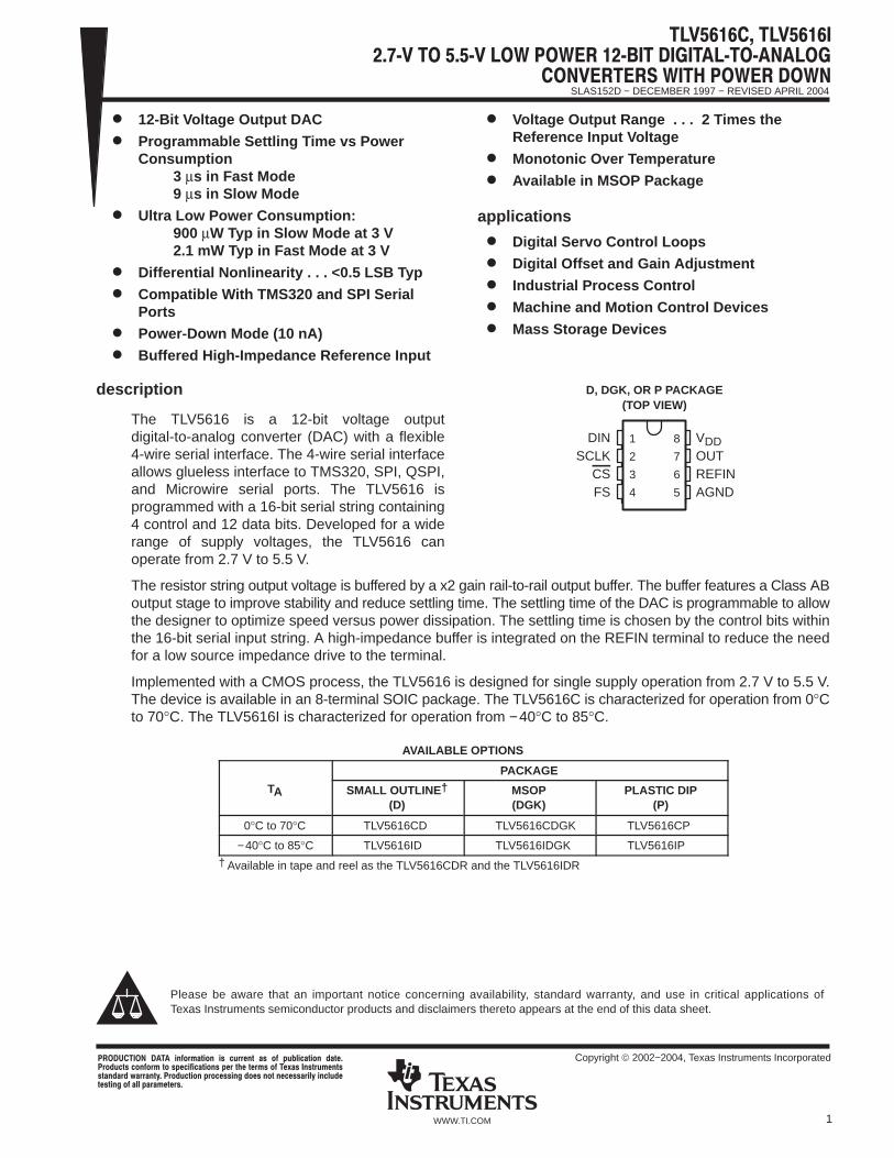
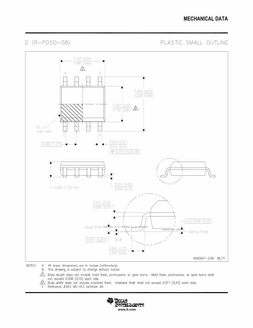
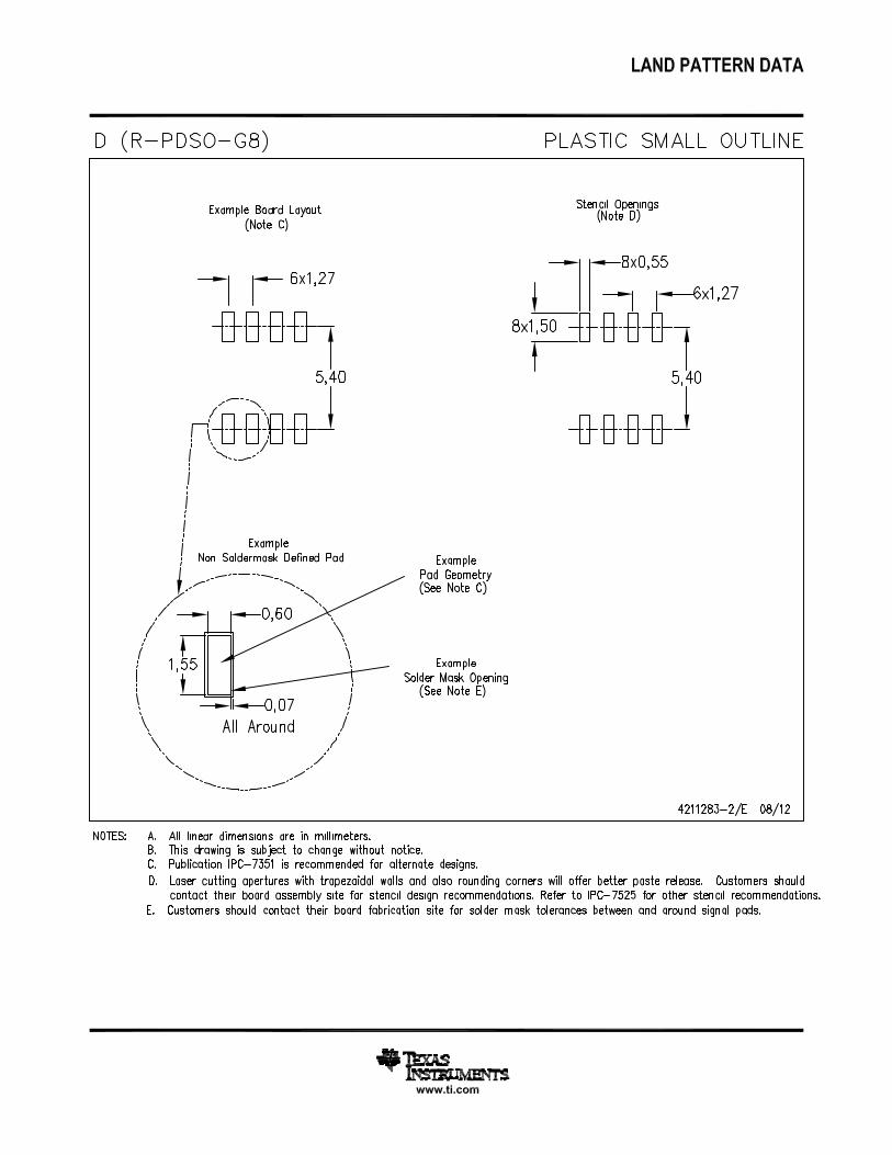
TLV5616C, TLV5616I 2.7ĆV TO 5.5ĆV LOW POWER 12ĆBIT DIGITALĆTOĆANALOG CONVERTERS WITH POWER DOWN SLAS152D - DECEMBER 1997 - REVISED APRIL 2004 1 WWW.TI.COM D 12-Bit Voltage Output DAC D Programmable Settling Time vs Power Consumption 3 µs in Fast Mode 9 µs in Slow Mode D Ultra Low Power Consumption: 900 µW Typ in Slow Mode at 3 V 2.1 mW Typ in Fast Mode at 3 V D Differential Nonlinearity . . . <0.5 LSB Typ D Compatible With TMS320 and SPI Serial Ports D Power-Down Mode (10 nA) D Buffered High-Impedance Reference Input D Voltage Output Range . . . 2 Times the Reference Input Voltage D Monotonic Over Temperature D Available in MSOP Package applications D Digital Servo Control Loops D Digital Offset and Gain Adjustment D Industrial Process Control D Machine and Motion Control Devices D Mass Storage Devices description The TLV5616 is a 12-bit voltage output digital-to-analog converter (DAC) with a flexible 4-wire serial interface. The 4-wire serial interface allows glueless interface to TMS320, SPI, QSPI, and Microwire serial ports. The TLV5616 is programmed with a 16-bit serial string containing 4 control and 12 data bits. Developed for a wide range of supply voltages, the TLV5616 can operate from 2.7 V to 5.5 V. The resistor string output voltage is buffered by a x2 gain rail-to-rail output buffer. The buffer features a Class AB output stage to improve stability and reduce settling time. The settling time of the DAC is programmable to allow the designer to optimize speed versus power dissipation. The settling time is chosen by the control bits within the 16-bit serial input string. A high-impedance buffer is integrated on the REFIN terminal to reduce the need for a low source impedance drive to the terminal. Implemented with a CMOS process, the TLV5616 is designed for single supply operation from 2.7 V to 5.5 V. The device is available in an 8-terminal SOIC package. The TLV5616C is characterized for operation from 0°C to 70°C. The TLV5616I is characterized for operation from -40°C to 85°C. AVAILABLE OPTIONS PACKAGE T A SMALL OUTLINE † (D) MSOP (DGK) PLASTIC DIP (P) 0°C to 70°C TLV5616CD TLV5616CDGK TLV5616CP -40°C to 85°C TLV5616ID TLV5616IDGK TLV5616IP † Available in tape and reel as the TLV5616CDR and the TLV5616IDR Please be aware that an important notice concerning availability, standard warranty, and use in critical applications of Texas Instruments semiconductor products and disclaimers thereto appears at the end of this data sheet. Copyright 2002-2004, Texas Instruments Incorporated PRODUCTION DATA information is current as of publication date. Products conform to specifications per the terms of Texas Instruments standard warranty. Production processing does not necessarily include testing of all parameters. 1 2 3 4 8 7 6 5 DIN SCLK CS FS V DD OUT REFIN AGND D, DGK, OR P PACKAGE (TOP VIEW)
Transcript
SLAS152D − DECEMBER 1997 − REVISED APRIL 2004
1WWW.TI.COM
12-Bit Voltage Output DAC
Programmable Settling Time vs PowerConsumption
3 µs in Fast Mode9 µs in Slow Mode
Ultra Low Power Consumption:900 µW Typ in Slow Mode at 3 V2.1 mW Typ in Fast Mode at 3 V
Differential Nonlinearit y . . . <0.5 LSB Typ
Compatible With TMS320 and SPI SerialPorts
Power-Down Mode (10 nA)
Buffered High-Impedance Reference Input
Voltage Output Range . . . 2 Times theReference Input Voltage
Monotonic Over Temperature
Available in MSOP Package
applications
Digital Servo Control Loops
Digital Offset and Gain Adjustment
Industrial Process Control
Machine and Motion Control Devices
Mass Storage Devices
description
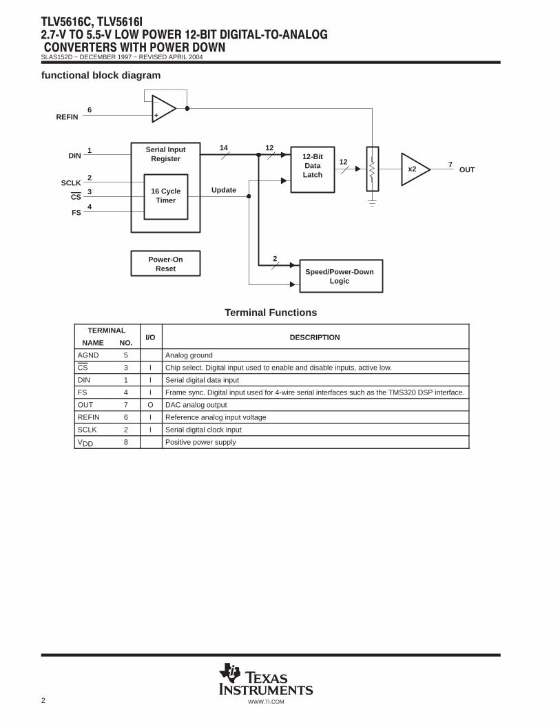
The TLV5616 is a 12-bit voltage outputdigital-to-analog converter (DAC) with a flexible4-wire serial interface. The 4-wire serial interfaceallows glueless interface to TMS320, SPI, QSPI,and Microwire serial ports. The TLV5616 isprogrammed with a 16-bit serial string containing4 control and 12 data bits. Developed for a widerange of supply voltages, the TLV5616 canoperate from 2.7 V to 5.5 V.
The resistor string output voltage is buffered by a x2 gain rail-to-rail output buffer. The buffer features a Class ABoutput stage to improve stability and reduce settling time. The settling time of the DAC is programmable to allowthe designer to optimize speed versus power dissipation. The settling time is chosen by the control bits withinthe 16-bit serial input string. A high-impedance buffer is integrated on the REFIN terminal to reduce the needfor a low source impedance drive to the terminal.
Implemented with a CMOS process, the TLV5616 is designed for single supply operation from 2.7 V to 5.5 V.The device is available in an 8-terminal SOIC package. The TLV5616C is characterized for operation from 0°Cto 70°C. The TLV5616I is characterized for operation from −40°C to 85°C.
AVAILABLE OPTIONS
PACKAGE
TA SMALL OUTLINE †
(D)MSOP(DGK)
PLASTIC DIP(P)
0°C to 70°C TLV5616CD TLV5616CDGK TLV5616CP
−40°C to 85°C TLV5616ID TLV5616IDGK TLV5616IP
† Available in tape and reel as the TLV5616CDR and the TLV5616IDR
Please be aware that an important notice concerning availability, standard warranty, and use in critical applications ofTexas Instruments semiconductor products and disclaimers thereto appears at the end of this data sheet.
† Stresses beyond those listed under “absolute maximum ratings” may cause permanent damage to the device. These are stress ratings only, andfunctional operation of the device at these or any other conditions beyond those indicated under “recommended operating conditions” is notimplied. Exposure to absolute-maximum-rated conditions for extended periods may affect device reliability.
recommended operating conditions
MIN NOM MAX UNIT
Supply voltage, VDDVDD = 5 V 4.5 5 5.5 V
Supply voltage, VDDVDD = 3 V 2.7 3 3.3 V
High-level digital input voltage, VIHDVDD = 2.7 V 2 V
High-level digital input voltage, VIHDVDD = 5.5 V 2.4 V
Low-level digital input voltage, VILDVDD = 2.7 V 0.6 V
Low-level digital input voltage, VILDVDD = 5.5 V 1 V
Reference voltage, Vref to REFIN terminal VDD = 5 V (see Note 1) AGND 2.048 VDD−1.5 V
Reference voltage, Vref to REFIN terminal VDD = 3 V (see Note 1) AGND 1.024 VDD−1.5 V
Load resistance, RL 2 10 kΩ
Load capacitance, CL 100 pF
Clock frequency, fCLK 20 MHz
Operating free-air temperature, TATLV5616C 0 70 °C
Operating free-air temperature, TATLV5616I −40 85 °C
NOTE 1: Due to the x2 output buffer, a reference input voltage ≥ VDD/2 causes clipping of the transfer function.
electrical characteristics over recommended operating free-air temperature range (unlessotherwise noted)
power supplyPARAMETER TEST CONDITIONS MIN TYP MAX UNIT
VDD = 5 V, VREF = 2.048 V,No load,
Fast 0.9 1.35 mA
IDD Power supply current
No load,All inputs = AGND or VDD,DAC latch = 0x800 Slow 0.4 0.6 mA
EZS Zero-scale error (offset error at zero scale) See Note 6 ±10 mV
Zero-scale-error temperature coefficient See Note 7 10 ppm/°C
EG Gain error See Note 8 ±0.6% ofFS
voltage
Gain-error temperature coefficient See Note 9 10 ppm/°C
NOTES: 4. The relative accuracy or integral nonlinearity (INL) sometimes referred to as linearity error, is the maximum deviation of the outputfrom the line between zero and full scale excluding the effects of zero code and full-scale errors. Tested from code 10 to code 4095.
5. The differential nonlinearity (DNL) sometimes referred to as differential error, is the difference between the measured and ideal 1LSB amplitude change of any two adjacent codes. Monotonic means the output voltage changes in the same direction (or remainsconstant) as a change in the digital input code. Tested from code 10 to code 4095.
6. Zero-scale error is the deviation from zero voltage output when the digital input code is zero.7. Zero-scale-error temperature coefficient is given by: EZS TC = [EZS (Tmax) − EZS (Tmin)]/Vref × 106/(Tmax − Tmin).8. Gain error is the deviation from the ideal output (2Vref − 1 LSB) with an output load of 10 kΩ excluding the effects of the zero-error.9. Gain temperature coefficient is given by: EG TC = [EG(Tmax) − EG (Tmin)]/Vref × 106/(Tmax − Tmin).
output specificationsPARAMETER TEST CONDITIONS MIN TYP MAX UNIT
VO Voltage output range RL = 10 kΩ 0 AVDD−0.1 V
Output load regulation accuracy RL = 2 kΩ, vs 10 kΩ 0.1 ±0.25% of FSvoltage
reference input (REF)PARAMETER TEST CONDITIONS MIN TYP MAX UNIT
THD Total harmonic distortionRL = 10 kΩ, CL = 100 pF,BW = 20 kHz −68 dB
Spurious free dynamic rangeBW = 20 kHz
70 dB
NOTES: 11. Settling time is the time for the output signal to remain within ±0.5 LSB of the final measured value for a digital input code changeof 0x080 to 0x3FF or 0x3FF to 0x080. Not tested, ensured by design.
12. Settling time is the time for the output signal to remain within ± 0.5 LSB of the final measured value for a digital input code changeof one count. Code change from 0x1FF to 0x200. Not tested, ensured by design.
13. Slew rate determines the time it takes for a change of the DAC output from 10% to 90% full-scale voltage.
digital input timing requirements
MIN NOM MAX UNIT
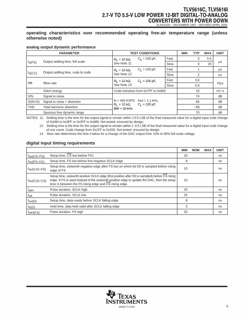
tsu(CS−FS) Setup time, CS low before FS↓ 10 ns
tsu(FS−CK) Setup time, FS low before first negative SCLK edge 8 ns
tsu(C16−FS)Setup time, sixteenth negative edge after FS low on which bit D0 is sampled before risingedge of FS
10 ns
tsu(C16−CS)
Setup time, sixteenth positive SCLK edge (first positive after D0 is sampled) before CS risingedge. If FS is used instead of the sixteenth positive edge to update the DAC, then the setuptime is between the FS rising edge and CS rising edge.
10 ns
twH Pulse duration, SCLK high 25 ns
twL Pulse duration, SCLK low 25 ns
tsu(D) Setup time, data ready before SCLK falling edge 8 ns
th(D) Hold time, data held valid after SCLK falling edge 5 ns
twH(FS) Pulse duration, FS high 20 ns
SLAS152D − DECEMBER 1997 − REVISED APRIL 2004
6 WWW.TI.COM
PARAMETER MEASUREMENT INFORMATION
ÎÎÎÎÎÎÎÎÎÎ
ÎÎÎÎÎÎ
ÎÎÎÎÎÎÎÎ
ÎÎÎÎÎÎÎÎ
1 2 3 4 5 15 16
D15 D14 D13 D12 D1 D0
tsu(FS-CK)
tsu(CS-FS)
twH(FS)
th(D)tsu(D)
twHtwL
tsu(C16-CS)
tsu(C16-FS)
SCLK
DIN
CS
FS
Figure 1. Timing Diagram
SLAS152D − DECEMBER 1997 − REVISED APRIL 2004
7WWW.TI.COM
TYPICAL CHARACTERISTICS
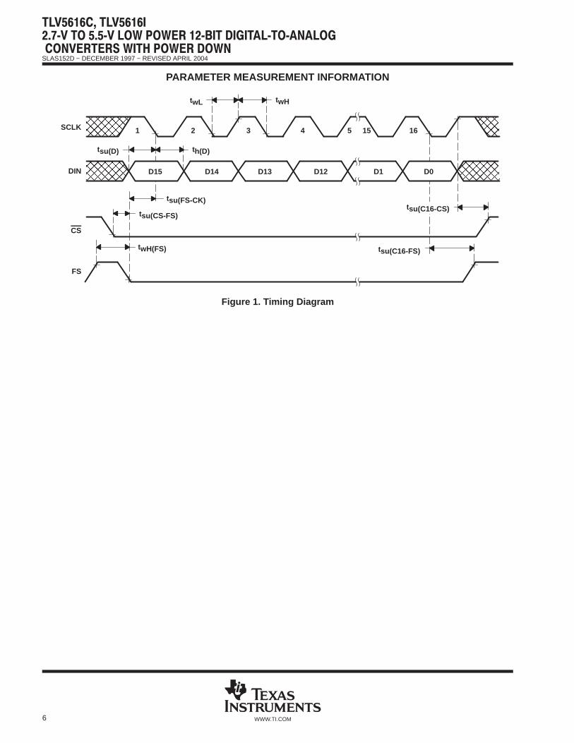
Figure 2
1.998
1.996
1.994
1.9900 0.01 0.02 0.05 0.1 0.2 0.5
− O
utpu
t Vol
tage
− V
2
2.002
Load Current − mA
OUTPUT VOLTAGEvs
LOAD CURRENT2.004
1 4
3 V Slow Mode, SOURCE
3 V Fast Mode, SOURCE
1.992
VO
VDD = 3 V,Vref = 1 V,Full Scale
2
Figure 3
3.995
3.99
3.985
3.9750 0.02 0.04 0.1 0.2 0.4 1
4
4.005
OUTPUT VOLTAGEvs
LOAD CURRENT4.01
2 4
3.98
− O
utpu
t Vol
tage
− V
Load Current − mA
5 V Slow Mode, SOURCE
5 V Fast Mode, SOURCE
VO
VDD = 5 V,Vref = 2 V,Full Scale
Figure 4
0.1
0.08
0.04
00 0.01 0.02 0.05 0.1 0.2 0.5
0.16
0.18
OUTPUT VOLTAGEvs
LOAD CURRENT
0.2
1 2
0.14
0.12
0.06
0.02
− O
utpu
t Vol
tage
− V
Load Current − mA
3 V Slow Mode, SINK
3 V Fast Mode, SINK
VO
VDD = 3 V,Vref = 1 V,Zero Code
Figure 5
0.2
0.15
0.1
00 0.02 0.04 0.1 0.2 0.4 1
0.25
0.3
OUTPUT VOLTAGEvs
LOAD CURRENT
0.35
2 4
0.05
− O
utpu
t Vol
tage
− V
Load Current − mA
5 V Slow Mode, SINK
5 V Fast Mode, SINK
VO
VDD = 5 V,Vref = 2 V,Zero Code
SLAS152D − DECEMBER 1997 − REVISED APRIL 2004
8 WWW.TI.COM
TYPICAL CHARACTERISTICS
Figure 6
0.6
0.4
0.2−55 −40 −25 0 25 40 70
− S
uppl
y C
urre
nt −
mA 0.8
SUPPLY CURRENTvs
FREE-AIR TEMPERATURE1
85 125
I DD
VDD = 3 V,Vref = 1 V,Full Scale
TA − Free-Air Temperature − C °
Fast Mode
Slow Mode
Figure 7
SUPPLY CURRENTvs
FREE-AIR TEMPERATURE
0.6
0.4
0.2−55 −40 −25 0 25 40 70
− S
uppl
y C
urre
nt −
mA 0.8
1
85 125
I DD
VDD = 5 V,Vref = 2 V, Full Scale
TA − Free-Air Temperature − C °
Fast Mode
Slow Mode
Figure 8
−−40
−50
−70
−800 5 10 20
TH
D −
Tot
al H
arm
onic
Dis
tort
ion
− dB
−30
−10
f − Frequency − kHz
TOTAL HARMONIC DISTORTIONvs
FREQUENCY0
30 50 100
−20
−60
Vref = 1 V dc + 1 V p/p Sinewave,Output Full Scale
Fast Mode
Figure 9
−−40
−50
−70
−800 5 10 20
TH
D −
Tot
al H
arm
onic
Dis
tort
ion
− dB
−30
−10
f − Frequency − kHz
TOTAL HARMONIC DISTORTIONvs
FREQUENCY0
30 50 100
−20
−60
Vref = 1 V dc + 1 V p/p Sinewave,Output Full Scale
Slow Mode
SLAS152D − DECEMBER 1997 − REVISED APRIL 2004
9WWW.TI.COM
TYPICAL CHARACTERISTICS
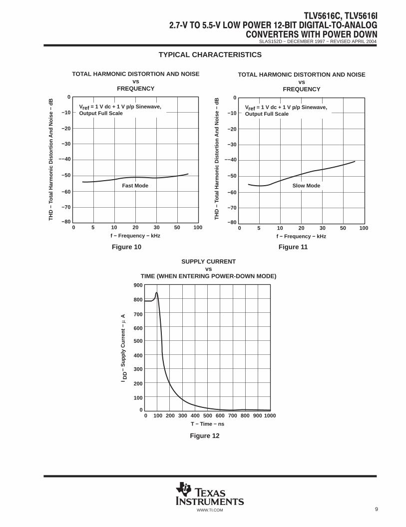
Figure 10
−−40
−50
−70
−800 5 10 20
TH
D −
Tot
al H
arm
onic
Dis
tort
ion
And
Noi
se −
dB
−30
−10
f − Frequency − kHz
TOTAL HARMONIC DISTORTION AND NOISEvs
FREQUENCY0
30 50 100
−20
−60
Vref = 1 V dc + 1 V p/p Sinewave,Output Full Scale
Fast Mode
Figure 11
−−40
−50
−70
−800 5 10 20
−30
−10
f − Frequency − kHz
TOTAL HARMONIC DISTORTION AND NOISEvs
FREQUENCY0
30 50 100
−20
−60
Vref = 1 V dc + 1 V p/p Sinewave,Output Full Scale
TH
D −
Tot
al H
arm
onic
Dis
tort
ion
And
Noi
se −
dB
Slow Mode
Figure 12
400
300
100
00 100 200 300 400 500 600
− S
uppl
y C
urre
nt − 600
800
T − Time − ns
SUPPLY CURRENTvs
TIME (WHEN ENTERING POWER-DOWN MODE)900
700 800 900 1000
700
500
200
I DD
µA
SLAS152D − DECEMBER 1997 − REVISED APRIL 2004
10 WWW.TI.COM
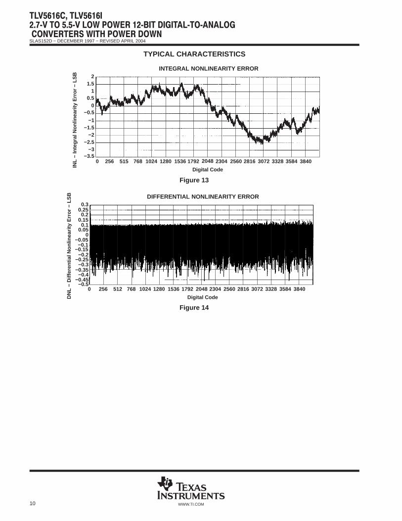
TYPICAL CHARACTERISTICS
−2
−3.50 256 768 1280 1536 1792 2304
−1
0.5
INTEGRAL NONLINEARITY ERROR2
2816 3328 3584
1.51
0−0.5
−1.5
−2.5−3
Digital Code
INL
− In
tegr
al N
onlin
earit
y E
rror
− L
SB
515 1024 2048 2560 3072 3840
Figure 13
0 256 512 768 1536 2048 2304
DN
L −
Diff
eren
tial N
onlin
earit
y E
rror
− L
SB
0.1
Digital Code
DIFFERENTIAL NONLINEARITY ERROR0.3
2560 3328 3584 3840
0.250.2
0.15
0.050
−0.05−0.1
−0.15−0.2
−0.25−0.3
−0.35−0.4
−0.45−0.5
1024 1280 1792 2816 3072
Figure 14
SLAS152D − DECEMBER 1997 − REVISED APRIL 2004
11WWW.TI.COM
APPLICATION INFORMATION
general function
The TLV5616 is a 12-bit single supply DAC based on a resistor string architecture. The device consists of a serialinterface, speed and power-down control logic, a reference input buffer, a resistor string, and a rail-to-rail outputbuffer.
The output voltage (full scale determined by external reference) is given by:
2 REF CODE2n [V]
where REF is the reference voltage and CODE is the digital input value within the range of 010 to 2n−1, wheren = 12 (bits). The 16-bit data word, consisting of control bits and the new DAC value, is illustrated in the dataformat section. A power-on reset initially resets the internal latches to a defined state (all bits zero).
serial interface
Explanation of data transfer: First, the device has to be enabled with CS set to low. Then, a falling edge of FSstarts shifting the data bit-per-bit (starting with the MSB) to the internal register on the falling edges of SCLK.After 16 bits have been transferred or FS rises, the content of the shift register is moved to the DAC latch whichupdates the voltage output to the new level.
The serial interface of the TLV5616 can be used in two basic modes:
Four wire (with chip select)
Three wire (without chip select)
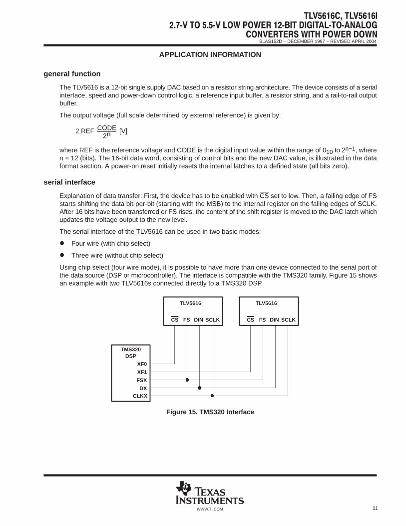
Using chip select (four wire mode), it is possible to have more than one device connected to the serial port ofthe data source (DSP or microcontroller). The interface is compatible with the TMS320 family. Figure 15 showsan example with two TLV5616s connected directly to a TMS320 DSP.
TMS320DSP
XF0
XF1
FSX
DXCLKX
TLV5616
CS FS DIN SCLK
TLV5616
CS FS DIN SCLK
Figure 15. TMS320 Interface
SLAS152D − DECEMBER 1997 − REVISED APRIL 2004
12 WWW.TI.COM
APPLICATION INFORMATION
serial interface (continued)
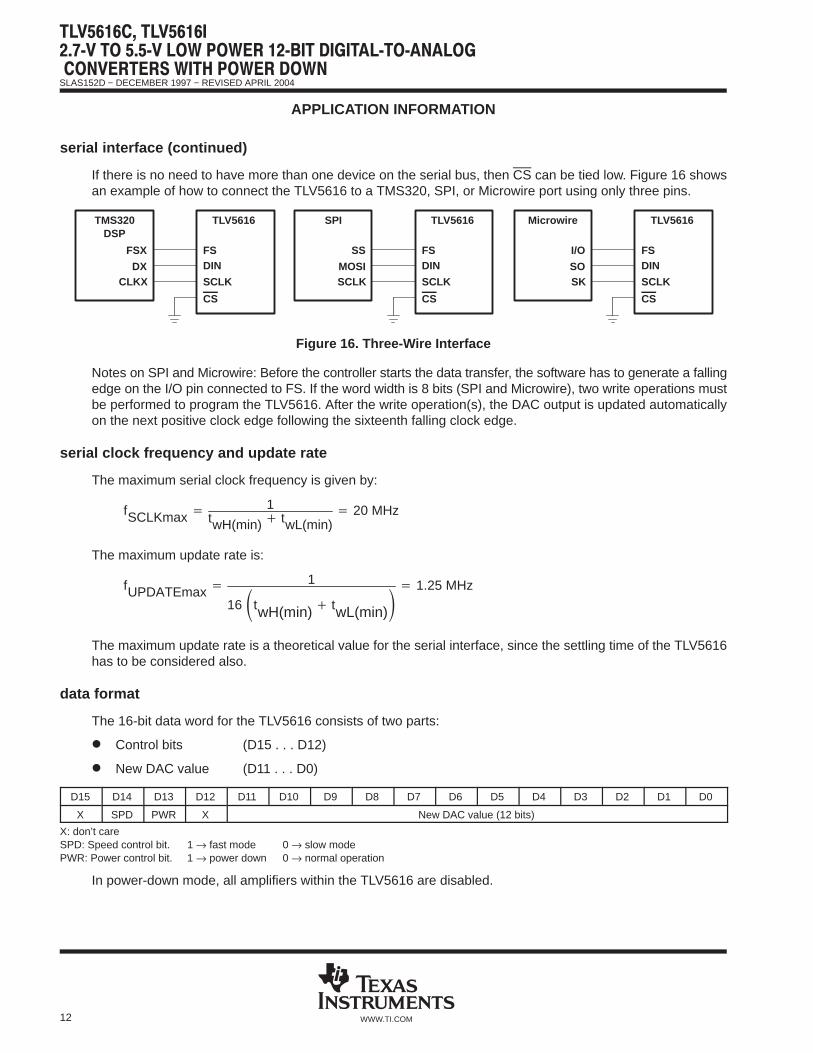
If there is no need to have more than one device on the serial bus, then CS can be tied low. Figure 16 showsan example of how to connect the TLV5616 to a TMS320, SPI, or Microwire port using only three pins.
TMS320DSP
FSX
DXCLKX
TLV5616
FSDIN
SCLK
CS
SPI
SS
MOSISCLK
TLV5616
FSDIN
SCLK
CS
Microwire
I/O
SOSK
TLV5616
FSDIN
SCLK
CS
Figure 16. Three-Wire Interface
Notes on SPI and Microwire: Before the controller starts the data transfer, the software has to generate a fallingedge on the I/O pin connected to FS. If the word width is 8 bits (SPI and Microwire), two write operations mustbe performed to program the TLV5616. After the write operation(s), the DAC output is updated automaticallyon the next positive clock edge following the sixteenth falling clock edge.
serial clock frequency and update rate
The maximum serial clock frequency is given by:
fSCLKmax 1twH(min) twL(min)
20 MHz
The maximum update rate is:
fUPDATEmax 1
16 twH(min) twL(min) 1.25 MHz
The maximum update rate is a theoretical value for the serial interface, since the settling time of the TLV5616has to be considered also.
data format
The 16-bit data word for the TLV5616 consists of two parts:
X: don’t careSPD: Speed control bit. 1 → fast mode 0 → slow modePWR: Power control bit. 1 → power down 0 → normal operation
In power-down mode, all amplifiers within the TLV5616 are disabled.
SLAS152D − DECEMBER 1997 − REVISED APRIL 2004
13WWW.TI.COM
APPLICATION INFORMATION
TLV5616 interfaced to TMS320C203 DSP
hardware interfacing
Figure 17 shows an example how to connect the TLV5616 to a TMS320C203 DSP. The serial interface of theTLV5616 is ideally suited to this configuration, using a maximum of four wires to make the necessaryconnections. In applications where only one synchronous serial peripheral is used, the interface can besimplified even further by pulling CS low all the time as shown in the figure.
FS
DIN
SCLK
OUTREFIN
CS AGND
VDD
REF
FS
DX
CLKX
TMS320C203 TLV5616
RLOAD
Figure 17. TLV5616 to DSP Interface
software
No setup procedure is needed to access the TLV5616. The output voltage can be set using just a singlecommand.
out data_addr, SDTR
where data_addr points to an address location holding the control bits and the 12 data bits providing the outputvoltage data. SDTR is the address of the transmit FIFO of the synchronous serial port.
The following code shows how to use the timer of the TMS320C203 as a time base to generate a voltage rampwith the TLV5616.
A timer interrupt is generated every 205 µs. The corresponding interrupt service routine increments the outputcode (stored at 0x0064) for the DAC, adds the DAC control bits to the four most significant bits, and writes thenew code to the TLV5616. The resulting period of the saw waveform is:
π = 4096 × 205 E-6 s = 0.84 s
;***************************************************************************************;* Title : Ramp generation with TLV5616 *;* Version : 1.0 *;* DSP : TI TMS320C203 *;* (1998) Texas Instruments Incorporated *;***************************************************************************************
;−−−−−−−−−−− I/O and memory mapped regs −−−−−−−−−−−−.include ”regs.asm”
;−−−−−−−−−−− vectors −−−−−−−−−−−−−−−−−−−−−−−−−−−−−−−.ps 0h b start b INT1 b INT23 b TIM_ISR
SLAS152D − DECEMBER 1997 − REVISED APRIL 2004
14 WWW.TI.COM
APPLICATION INFORMATION
;***************************************************************************************;* Main Program;***************************************************************************************
; all else fails stop heredone: b done ;hang there
;***************************************************************************************;* Interrupt Service Routines;***************************************************************************************INT1: ret ;do nothing and return
INT23: ret ;do nothing and return
TIM_ISR:lacl 64h ; restore counter value to ACCadd #1h ; increment DAC valueand #0FFFh ; mask 4 MSBssacl 64h ; store 12 bit counter valueor #4000h ; set DAC control bitssacl 65h ; store DAC valueout 65h, SDTR ; send data
clrc intm ; re-enable interruptsret
.END
SLAS152D − DECEMBER 1997 − REVISED APRIL 2004
15WWW.TI.COM
APPLICATION INFORMATION
TLV5616 interfaced to MCS51 microcontroller
hardware interfacing
Figure 18 shows an example of how to connect the TLV5616 to an MCS51 compatible microcontroller. Theserial DAC input data and external control signals are sent via I/O port 3 of the controller. The serial data is senton the RxD line, with the serial clock output on the TxD line. P3.4 and P3.5 are configured as outputs to providethe chip select and frame sync signals for the TLV5616.
SDIN
SCLK
CS
OUT
REFIN
AGND
REF
RxD
TxD
P3.4
MCS51 Controller TLV5616
FSP3.5
VDD
RLOAD
Figure 18. TLV5616 to MCS51 Controller Interface
software
The example program puts out a sine wave on the OUT pin.
The on-chip timer is used to generate interrupts at a fixed frequency. The related interrupt service routine fetchesand writes the next sample to the DAC. The samples are stored in a lookup table, which describes one full periodof a sine wave.
The serial port of the controller is used in mode 0, which transmits 8 bits of data on RxD, accompanied by asynchronous clock on TxD. Two writes concatenated together are required to write a complete word to theTLV5616. The CS and FS signals are provided in the required fashion through control of I/O port 3, which hasbit addressable outputs.
;***************************************************************************************;* Title : Ramp generation with TLV5616 *;* Version : 1.0 *;* MCU : INTEL MCS51 *;* (1998) Texas Instruments Incorporated *;***************************************************************************************
;−−−−−−−−−−−−−−−−−−−−−−−−−−−−−−−−−−−−−−−−−−−−−−−−−−−−−−−−−−−−−−−−−−−−−−−−−−−−−−−−−−−−−−−; Program function declaration;−−−−−−−−−−−−−−−−−−−−−−−−−−−−−−−−−−−−−−−−−−−−−−−−−−−−−−−−−−−−−−−−−−−−−−−−−−−−−−−−−−−−−−−
;−−−−−−−−−−−−−−−−−−−−−−−−−−−−−−−−−−−−−−−−−−−−−−−−−−−−−−−−−−−−−−−−−−−−−−−−−−−−−−−−−−−−−−−; Code start at address 0, jump to start;−−−−−−−−−−−−−−−−−−−−−−−−−−−−−−−−−−−−−−−−−−−−−−−−−−−−−−−−−−−−−−−−−−−−−−−−−−−−−−−−−−−−−−−
CSEG AT 0
MCS is a registered trademark of Intel Corporation
SLAS152D − DECEMBER 1997 − REVISED APRIL 2004
16 WWW.TI.COM
APPLICATION INFORMATION
LJMP start ; Execution starts at address 0 on power−up.
;−−−−−−−−−−−−−−−−−−−−−−−−−−−−−−−−−−−−−−−−−−−−−−−−−−−−−−−−−−−−−−−−−−−−−−−−−−−−−−−−−−−−−−−; Code in the timer0 interrupt vector;−−−−−−−−−−−−−−−−−−−−−−−−−−−−−−−−−−−−−−−−−−−−−−−−−−−−−−−−−−−−−−−−−−−−−−−−−−−−−−−−−−−−−−−
CSEG AT 0BH
LJMP timer0isr ; Jump vector for timer 0 interrupt is 000Bh
;−−−−−−−−−−−−−−−−−−−−−−−−−−−−−−−−−−−−−−−−−−−−−−−−−−−−−−−−−−−−−−−−−−−−−−−−−−−−−−−−−−−−−−−; Define program variables;−−−−−−−−−−−−−−−−−−−−−−−−−−−−−−−−−−−−−−−−−−−−−−−−−−−−−−−−−−−−−−−−−−−−−−−−−−−−−−−−−−−−−−−
RSEG VAR1
rolling_ptr: DS 1
;−−−−−−−−−−−−−−−−−−−−−−−−−−−−−−−−−−−−−−−−−−−−−−−−−−−−−−−−−−−−−−−−−−−−−−−−−−−−−−−−−−−−−−−; Interrupt service routine for timer 0 interrupts;−−−−−−−−−−−−−−−−−−−−−−−−−−−−−−−−−−−−−−−−−−−−−−−−−−−−−−−−−−−−−−−−−−−−−−−−−−−−−−−−−−−−−−−
RSEG ISR
timer0isr:
PUSH PSWPUSH ACC
CLR T0 ; set CSB lowCLR T1 ; set FS low
; The signal to be output on the dac is a sine function. One cycle of a sine wave is ; held in a table @ sinevals as 32 samples of msb, lsb pairs (64 bytes). The pointer,; rolling_ptr, rolls round the table of samples incrementing by 2 bytes (1 sample) on; each interrupt (at the end of this routine).
MOV DPTR,#sinevals ; set DPTR to the start of the table of sine signal valuesMOV A,rolling_ptr ; ACC loaded with the pointer into the sine table
MOVC A,@A+DPTR ; get msb from the tableORL A, #00H ; set control bits MOV SBUF,A ; send out msb of data word
MOV A,rolling_ptr; move rolling pointer in to ACCINC A ; increment ACC holding the rolling pointerMOVC A,@A+DPTR ; which is the lsb of this sample, now in ACC
MSB_TX:JNB TI, MSB_TX ; wait for transmit to completeCLR TI ; clear for new transmitMOV SBUF,A ; and send out the lsb
LSB_TX:JNB TI, LSB_TX ; wait for lsb transmit to completeSETB T1 ; set FS = 1CLR TI ; clear for new transmit
MOV A,rolling_ptr ; load ACC with rolling pointerINC A ; increment the ACC twice, to get next sampleINC AANL A,#03FH ; wrap back round to 0 if >64MOV rolling_ptr,A ; move value held in ACC back to the rolling pointer
SETB T0 ; CSB high
POP ACCPOP PSW
RETI
;−−−−−−−−−−−−−−−−−−−−−−−−−−−−−−−−−−−−−−−−−−−−−−−−−−−−−−−−−−−−−−−−−−−−−−−−−−−−−−−; Set up stack;−−−−−−−−−−−−−−−−−−−−−−−−−−−−−−−−−−−−−−−−−−−−−−−−−−−−−−−−−−−−−−−−−−−−−−−−−−−−−−−
SLAS152D − DECEMBER 1997 − REVISED APRIL 2004
17WWW.TI.COM
APPLICATION INFORMATION
RSEG STACKDS 10h ; 16 Byte Stack!
;−−−−−−−−−−−−−−−−−−−−−−−−−−−−−−−−−−−−−−−−−−−−−−−−−−−−−−−−−−−−−−−−−−−−−−−−−−−−−−−; Main Program;−−−−−−−−−−−−−−−−−−−−−−−−−−−−−−−−−−−−−−−−−−−−−−−−−−−−−−−−−−−−−−−−−−−−−−−−−−−−−−−
RSEG MAIN
start:MOV SP,#STACK−1 ; first set Stack Pointer
CLR AMOV SCON,A ; set serial port 0 to mode 0MOV TMOD,#02H ; set timer 0 to mode 2 − auto−reloadMOV TH0,#0C8H ; set TH0 for 16.67 kHs interrupts
SETB T1 ; set FS = 1SETB T0 ; set CSB = 1
SETB ET0 ; enable timer 0 interruptsSETB EA ; enable all interrupts
MOV rolling_ptr,A ; set rolling pointer to 0SETB TR0 ; start timer 0
always:SJMP always ; while(1) !RET
;−−−−−−−−−−−−−−−−−−−−−−−−−−−−−−−−−−−−−−−−−−−−−−−−−−−−−−−−−−−−−−−−−−−−−−−−−−−−−−−; Table of 32 sine wave samples used as DAC data;−−−−−−−−−−−−−−−−−−−−−−−−−−−−−−−−−−−−−−−−−−−−−−−−−−−−−−−−−−−−−−−−−−−−−−−−−−−−−−−
linearity, offset, and gain error using single ended supplies
When an amplifier is operated from a single supply, the voltage offset can still be either positive or negative. Witha positive offset, the output voltage changes on the first code change. With a negative offset, the output voltagemay not change with the first code, depending on the magnitude of the offset voltage.
The output amplifier attempts to drive the output to a negative voltage. However, because the most negativesupply rail is ground, the output cannot drive below ground and clamps the output at 0 V.
The output voltage then remains at zero until the input code value produces a sufficient positive output voltageto overcome the negative offset voltage, resulting in the transfer function shown in Figure 19.
DAC Code
OutputVoltage
0 V
NegativeOffset
Figure 19. Effect of Negative Offset (Single Supply)
This offset error, not the linearity error, produces this breakpoint. The transfer function would have followed thedotted line if the output buffer could drive below the ground rail.
For a DAC, linearity is measured between zero-input code (all inputs 0) and full-scale code (all inputs 1) afteroffset and full scale are adjusted out or accounted for in some way. However, single supply operation does notallow for adjustment when the offset is negative due to the breakpoint in the transfer function. So the linearityis measured between full-scale code and the lowest code that produces a positive output voltage.
power-supply bypassing and ground management
Printed-circuit boards that use separate analog and digital ground planes offer the best system performance.Wire-wrap boards do not perform well and should not be used. The two ground planes should be connectedtogether at the low-impedance power-supply source. The best ground connection may be achieved byconnecting the DAC AGND terminal to the system analog ground plane, making sure that analog groundcurrents are well managed and there are negligible voltage drops across the ground plane.
A 0.1-µF ceramic-capacitor bypass should be connected between VDD and AGND and mounted with short leadsas close as possible to the device. Use of ferrite beads may further isolate the system analog supply from thedigital power supply.
Figure 20 shows the ground plane layout and bypassing technique.
0.1 µF
Analog Ground Plane
1
2
3
4
8
7
6
5
Figure 20. Power-Supply Bypassing
SLAS152D − DECEMBER 1997 − REVISED APRIL 2004
19WWW.TI.COM
APPLICATION INFORMATION
definitions of specifications and terminology
integral nonlinearity (INL)
The relative accuracy or integral nonlinearity (INL), sometimes referred to as linearity error, is the maximumdeviation of the output from the line between zero and full scale excluding the effects of zero code and full-scaleerrors.
differential nonlinearity (DNL)
The differential nonlinearity (DNL), sometimes referred to as differential error, is the difference between themeasured and ideal 1 LSB amplitude change of any two adjacent codes. Monotonic means the output voltagechanges in the same direction (or remains constant) as a change in the digital input code.
zero-scale error (E ZS)
Zero-scale error is defined as the deviation of the output from 0 V at a digital input value of 0.
gain error (E G)
Gain error is the error in slope of the DAC transfer function.
signal-to-noise ratio + distortion (S/N+D)
S/N+D is the ratio of the rms value of the output signal to the rms sum of all other spectral components belowthe Nyquist frequency, including harmonics but excluding dc. The value for S/N+D is expressed in decibels.
spurious free dynamic range (SFDR)
SFDR is the difference between the rms value of the output signal and the rms value of the largest spurioussignal within a specified bandwidth. The value for SFDR is expressed in decibels.
total harmonic distortion (THD)
THD is the ratio of the rms sum of the first six harmonic components to the rms value of the fundamental signaland is expressed in decibels.
PACKAGE OPTION ADDENDUM
www.ti.com 10-Jun-2014
Addendum-Page 1
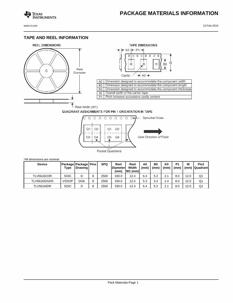
PACKAGING INFORMATION
Orderable Device Status(1)
Package Type PackageDrawing
Pins PackageQty
Eco Plan(2)
Lead/Ball Finish(6)
MSL Peak Temp(3)
Op Temp (°C) Device Marking(4/5)
Samples
TLV5616CD ACTIVE SOIC D 8 75 Green (RoHS& no Sb/Br)
CU NIPDAU Level-1-260C-UNLIM 0 to 70 5616C
TLV5616CDG4 ACTIVE SOIC D 8 75 Green (RoHS& no Sb/Br)
CU NIPDAU Level-1-260C-UNLIM 0 to 70 5616C
TLV5616CDGK ACTIVE VSSOP DGK 8 80 Green (RoHS& no Sb/Br)
CU NIPDAUAG Level-1-260C-UNLIM 0 to 70 ABF
TLV5616CDR ACTIVE SOIC D 8 2500 Green (RoHS& no Sb/Br)
CU NIPDAU Level-1-260C-UNLIM 0 to 70 5616C
TLV5616CDRG4 ACTIVE SOIC D 8 2500 Green (RoHS& no Sb/Br)
CU NIPDAU Level-1-260C-UNLIM 0 to 70 5616C
TLV5616CP ACTIVE PDIP P 8 50 Pb-Free(RoHS)
CU NIPDAU N / A for Pkg Type 0 to 70 TLV5616CP
TLV5616CPE4 ACTIVE PDIP P 8 50 Pb-Free(RoHS)
CU NIPDAU N / A for Pkg Type 0 to 70 TLV5616CP
TLV5616ID ACTIVE SOIC D 8 75 Green (RoHS& no Sb/Br)
CU NIPDAU Level-1-260C-UNLIM -40 to 85 5616I
TLV5616IDG4 ACTIVE SOIC D 8 75 Green (RoHS& no Sb/Br)
CU NIPDAU Level-1-260C-UNLIM -40 to 85 5616I
TLV5616IDGK ACTIVE VSSOP DGK 8 80 Green (RoHS& no Sb/Br)
CU NIPDAUAG Level-1-260C-UNLIM -40 to 85 AJE
TLV5616IDGKG4 ACTIVE VSSOP DGK 8 80 Green (RoHS& no Sb/Br)
CU NIPDAUAG Level-1-260C-UNLIM -40 to 85 AJE
TLV5616IDGKR ACTIVE VSSOP DGK 8 2500 Green (RoHS& no Sb/Br)
CU NIPDAUAG Level-1-260C-UNLIM -40 to 85 AJE
TLV5616IDR ACTIVE SOIC D 8 2500 Green (RoHS& no Sb/Br)
CU NIPDAU Level-1-260C-UNLIM -40 to 85 5616I
TLV5616IP ACTIVE PDIP P 8 50 Pb-Free(RoHS)
CU NIPDAU N / A for Pkg Type -40 to 85 TLV5616IP
(1) The marketing status values are defined as follows:ACTIVE: Product device recommended for new designs.LIFEBUY: TI has announced that the device will be discontinued, and a lifetime-buy period is in effect.NRND: Not recommended for new designs. Device is in production to support existing customers, but TI does not recommend using this part in a new design.PREVIEW: Device has been announced but is not in production. Samples may or may not be available.OBSOLETE: TI has discontinued the production of the device.
(2) Eco Plan - The planned eco-friendly classification: Pb-Free (RoHS), Pb-Free (RoHS Exempt), or Green (RoHS & no Sb/Br) - please check http://www.ti.com/productcontent for the latest availabilityinformation and additional product content details.TBD: The Pb-Free/Green conversion plan has not been defined.Pb-Free (RoHS): TI's terms "Lead-Free" or "Pb-Free" mean semiconductor products that are compatible with the current RoHS requirements for all 6 substances, including the requirement thatlead not exceed 0.1% by weight in homogeneous materials. Where designed to be soldered at high temperatures, TI Pb-Free products are suitable for use in specified lead-free processes.Pb-Free (RoHS Exempt): This component has a RoHS exemption for either 1) lead-based flip-chip solder bumps used between the die and package, or 2) lead-based die adhesive used betweenthe die and leadframe. The component is otherwise considered Pb-Free (RoHS compatible) as defined above.Green (RoHS & no Sb/Br): TI defines "Green" to mean Pb-Free (RoHS compatible), and free of Bromine (Br) and Antimony (Sb) based flame retardants (Br or Sb do not exceed 0.1% by weightin homogeneous material)
(3) MSL, Peak Temp. - The Moisture Sensitivity Level rating according to the JEDEC industry standard classifications, and peak solder temperature.
(4) There may be additional marking, which relates to the logo, the lot trace code information, or the environmental category on the device.
(5) Multiple Device Markings will be inside parentheses. Only one Device Marking contained in parentheses and separated by a "~" will appear on a device. If a line is indented then it is a continuationof the previous line and the two combined represent the entire Device Marking for that device.
(6) Lead/Ball Finish - Orderable Devices may have multiple material finish options. Finish options are separated by a vertical ruled line. Lead/Ball Finish values may wrap to two lines if the finishvalue exceeds the maximum column width.
Important Information and Disclaimer:The information provided on this page represents TI's knowledge and belief as of the date that it is provided. TI bases its knowledge and belief on informationprovided by third parties, and makes no representation or warranty as to the accuracy of such information. Efforts are underway to better integrate information from third parties. TI has taken andcontinues to take reasonable steps to provide representative and accurate information but may not have conducted destructive testing or chemical analysis on incoming materials and chemicals.TI and TI suppliers consider certain information to be proprietary, and thus CAS numbers and other limited information may not be available for release.
In no event shall TI's liability arising out of such information exceed the total purchase price of the TI part(s) at issue in this document sold by TI to Customer on an annual basis.
Texas Instruments Incorporated and its subsidiaries (TI) reserve the right to make corrections, enhancements, improvements and otherchanges to its semiconductor products and services per JESD46, latest issue, and to discontinue any product or service per JESD48, latestissue. Buyers should obtain the latest relevant information before placing orders and should verify that such information is current andcomplete. All semiconductor products (also referred to herein as “components”) are sold subject to TI’s terms and conditions of salesupplied at the time of order acknowledgment.TI warrants performance of its components to the specifications applicable at the time of sale, in accordance with the warranty in TI’s termsand conditions of sale of semiconductor products. Testing and other quality control techniques are used to the extent TI deems necessaryto support this warranty. Except where mandated by applicable law, testing of all parameters of each component is not necessarilyperformed.TI assumes no liability for applications assistance or the design of Buyers’ products. Buyers are responsible for their products andapplications using TI components. To minimize the risks associated with Buyers’ products and applications, Buyers should provideadequate design and operating safeguards.TI does not warrant or represent that any license, either express or implied, is granted under any patent right, copyright, mask work right, orother intellectual property right relating to any combination, machine, or process in which TI components or services are used. Informationpublished by TI regarding third-party products or services does not constitute a license to use such products or services or a warranty orendorsement thereof. Use of such information may require a license from a third party under the patents or other intellectual property of thethird party, or a license from TI under the patents or other intellectual property of TI.Reproduction of significant portions of TI information in TI data books or data sheets is permissible only if reproduction is without alterationand is accompanied by all associated warranties, conditions, limitations, and notices. TI is not responsible or liable for such altereddocumentation. Information of third parties may be subject to additional restrictions.Resale of TI components or services with statements different from or beyond the parameters stated by TI for that component or servicevoids all express and any implied warranties for the associated TI component or service and is an unfair and deceptive business practice.TI is not responsible or liable for any such statements.Buyer acknowledges and agrees that it is solely responsible for compliance with all legal, regulatory and safety-related requirementsconcerning its products, and any use of TI components in its applications, notwithstanding any applications-related information or supportthat may be provided by TI. Buyer represents and agrees that it has all the necessary expertise to create and implement safeguards whichanticipate dangerous consequences of failures, monitor failures and their consequences, lessen the likelihood of failures that might causeharm and take appropriate remedial actions. Buyer will fully indemnify TI and its representatives against any damages arising out of the useof any TI components in safety-critical applications.In some cases, TI components may be promoted specifically to facilitate safety-related applications. With such components, TI’s goal is tohelp enable customers to design and create their own end-product solutions that meet applicable functional safety standards andrequirements. Nonetheless, such components are subject to these terms.No TI components are authorized for use in FDA Class III (or similar life-critical medical equipment) unless authorized officers of the partieshave executed a special agreement specifically governing such use.Only those TI components which TI has specifically designated as military grade or “enhanced plastic” are designed and intended for use inmilitary/aerospace applications or environments. Buyer acknowledges and agrees that any military or aerospace use of TI componentswhich have not been so designated is solely at the Buyer's risk, and that Buyer is solely responsible for compliance with all legal andregulatory requirements in connection with such use.TI has specifically designated certain components as meeting ISO/TS16949 requirements, mainly for automotive use. In any case of use ofnon-designated products, TI will not be responsible for any failure to meet ISO/TS16949.
Products ApplicationsAudio www.ti.com/audio Automotive and Transportation www.ti.com/automotiveAmplifiers amplifier.ti.com Communications and Telecom www.ti.com/communicationsData Converters dataconverter.ti.com Computers and Peripherals www.ti.com/computersDLP® Products www.dlp.com Consumer Electronics www.ti.com/consumer-appsDSP dsp.ti.com Energy and Lighting www.ti.com/energyClocks and Timers www.ti.com/clocks Industrial www.ti.com/industrialInterface interface.ti.com Medical www.ti.com/medicalLogic logic.ti.com Security www.ti.com/securityPower Mgmt power.ti.com Space, Avionics and Defense www.ti.com/space-avionics-defenseMicrocontrollers microcontroller.ti.com Video and Imaging www.ti.com/videoRFID www.ti-rfid.comOMAP Applications Processors www.ti.com/omap TI E2E Community e2e.ti.comWireless Connectivity www.ti.com/wirelessconnectivity