Function commands - 0x14: READ MEMORY BAE0910 Multi-function 1-wire slave device i/o, adc, pwm, rtc, counter, EEPROM Microcontroller based 1-wire slave implementation for flexible solutions. Main features Pin and connections Five I/O pins allows various functions: One to four 16 bits PWM: two hardware (PWM1 & 2) + two software(PWM3 & 4) One 8 bits ADC input 0 to 5V One 32 bits counter One strong (20mA) digital output One PIO, software selectable as INPUT or OUTPUT (20ma) Compatibility with 1-wire protocol: Standard speed operation: protocol implemented with low latency interrupts in background. Support every standard ROM commands: read rom, match rom, search rom, skip rom, resume rom, conditional search Unique serial number Family code 0xFC: future devices will use this family code. The read_type & read_version commands expose allow determining the model/revision. Control functions: see FUNCTION COMMANDS page Physical characteristics: www.pbae.be BAE0910 Multi-function 1-wire slave device page 1 PIN NAME DESCRIPTION 1 COUNTER Selectable rising or falling edges counter. U u p to 10KHz. 2 OUTPUT/SPWM3 Simple output or SPWM3 (software Pulse Width Modulation) Capable of sourcing and sinking up to 20mA 3 VCC Power supply 2,7V to 5,5V 8mA typical consumption @ 5V 4 GND Ground 5 DQ 1-Wire interface open drain 6 PIO/SPWM4 PIO or SPWM4 (software Pulse Width Modulation ) Input mode: Configurable i I nternal pullup/pulldown 37KΩ resistor of 37KΩ Output mode: Capable of sourcing and sinking up to 20mA 7 ADC/PWM2 Analog to Digiti al Converter 8 bit :
Transcript
Function commands - 0x14: READ MEMORY
BAE0910 Multi-function 1-wire slave device
i/o, adc, pwm, rtc, counter, EEPROM Microcontroller based 1-wire slave implementation for flexible solutions.
Main features
Pin and connections
Five I/O pins allows various functions:
One to four 16 bits PWM: two hardware (PWM1 & 2) + two software(PWM3 & 4) One 8 bits ADC input 0 to 5V One 32 bits counter One strong (20mA) digital output One PIO, software selectable as INPUT or OUTPUT (20ma)
Compatibility with 1-wire protocol:
Standard speed operation: protocol implemented with low latency interrupts in background. Support every standard ROM commands: read rom, match rom, search rom, skip rom, resume
rom, conditional search Unique serial number Family code 0xFC: future devices will use this family code. The read_type & read_version
commands exposeallow determining the model/revision. Control functions: see FUNCTION COMMANDS page
Physical characteristics:
Single chip microcontroller based solution in an 8-pin SOIC. 5.0V supply voltage, 8mA typical consumption powerful 32MHz operation Fully functional without additional external components
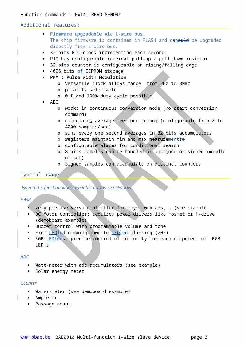
Firmware upgradable via 1-wire bus.The chip firmware is contained in FLASH and canould be upgraded directly from 1-wire bus.
32 bits RTC clock incrementing each second. PIO has configurable internal pull-up / pull-down resistor 32 bits counter is configurable on rising/falling edge 4096 bits of EEPROM storage PWM : Pulse Width Modulation
o Versatile clock allows range from 2Hz to 8MHz o polarity selectableo 0 % and 100% duty cycle possible
ADCo works in continuous conversion mode (no start conversion command)o calculates average over one second (configurable from 2 to 4000 samples/sec)o sums every one second averages in 32 bits accumulators o registers maintain min and max measurementsdo configurable alarms for conditional searcho 8 bits samples can be handled as unsigned or signed (middle offset)o Signed samples can accumulate on distinct counters
Typical usage
Extend the functionalities available on 1-wire networks
PWM
very precise servo controller for toys, webcams, … (see example) DC Motor controller; requires power drivers like mosfet or H-drive (demoboard example) Buzzer control with programmable volume and tone From LEDled dimming down to LEDled blinking (2Hz) RGB LEDleds: precise control of intensity for each component of RGB LED’s
ADC
Watt-meter with adc accumulators (see example) Solar energy meter
Counter
Water-meter (see demoboard example) Ampmeter Passage count
Main features.............................................................................................................................................................1Pin and connections................................................................................................................................................1 Five I/O pins allows various functions:..................................................................................................................1Compatibility with 1-wire protocol:........................................................................................................................1Physical characteristics:..........................................................................................................................................1Additional features:................................................................................................................................................2Typical usage...........................................................................................................................................................2
Table of Contents.......................................................................................................................................................3Hierarchical structure.................................................................................................................................................4Function commands...................................................................................................................................................5
0x11: READ VERSION .............................................................................................................................................50x12: READ TYPE ....................................................................................................................................................50x16: ERASE EEPROM PAGE ...................................................................................................................................50x14: READ MEMORY ............................................................................................................................................70x15: WRITE MEMORY ...........................................................................................................................................70x13: EXTENDED COMMAND .................................................................................................................................7
READ TYPE 0x12 1st byte device type=0x022nd byte chip type=0x01
Extended command 0x13Read block of <len> bytes 0x14Write block of <len> bytes 0x15 Erase eeprom page 0x16
0xFC specific firmware function
BAE0910 specific control function commands
1-Wire ROM functions commands
Function commands
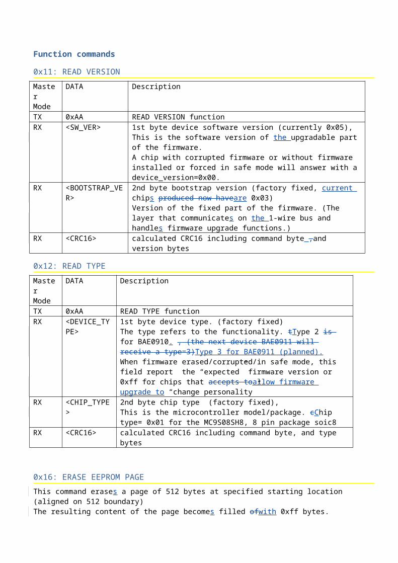
0x11: READ VERSION
Master Mode
DATA Description
TX 0xAA READ VERSION functionRX <SW_VER> 1st byte device software version (currently 0x05),
This is the software version of the upgradable part of the firmware. A chip with corrupted firmware or without firmware installed or forced in safe mode will answer with a device_version=0x00.
RX <BOOTSTRAP_VER> 2nd byte bootstrap version (factory fixed, current chips produced now haveare 0x03) Version of the fixed part of the firmware. (The layer that communicates on the 1-wire bus and handles firmware upgrade functions.)
RX <CRC16> calculated CRC16 including command byte ,and version bytes
The type refers to the functionality. tType 2 is for BAE0910. , (the next device BAE0911 will receive a type=3)Type 3 for BAE0911 (planned).When firmware erased/corrupted/in safe mode, this field report the “expected” firmware version or 0xff for chips that accepts toallow firmware upgrade to “change personality”
RX <CHIP_TYPE> 2nd byte chip type (factory fixed),This is the microcontroller model/package. cChip type= 0x01 for the MC9S08SH8, 8 pin package soic8
RX <CRC16> calculated CRC16 including command byte, and type bytes
0x16: ERASE EEPROM PAGE
This command erases a page of 512 bytes at specified starting location (aligned on 512 boundary) The resulting content of the page becomes filled ofwith 0xff bytes.
Master Mode
DATA Description
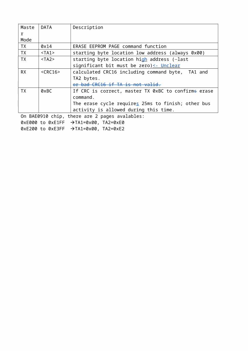
TX 0x14 ERASE EEPROM PAGE command function TX <TA1> starting byte location low address (always 0x00)TX <TA2> starting byte location high address ( last significant bit must be zero)<-
UnclearRX <CRC16> calculated CRC16 including command byte, TA1 and TA2 bytes.
or bad CRC16 if TA is not valid.TX 0xBC If CRC is correct, master TX 0xBC to confirms erase command.
The erase cycle requires 25ms to finish; other bus activity is allowed during this time.
On BAE0910 chip, there are 2 pages avalables:0xE000 to 0xE1FF TA1=0x00, TA2=0xE00xE200 to 0xE3FF TA1=0x00, TA2=0xE2
0x14: READ MEMORY
Master Mode
DATA Description
TX 0xAA READ MEMORY functionTX <TA1> starting byte location low addressTX <TA2> starting byte location hi addressTX <LEN> Length of data to read (max 32 bytes)RX <data bytes> <LEN> Bytes beginning at specified address RX <CRC16> calculated CRC16 including command byte, address, data bytesRead memory command allows to reading at botheither registers locations (TA =0x0000 to 0x007F) andor EEPROM data (TA=0xE000 to 0xE3FF)
0x15: WRITE MEMORY
Master Mode
DATA Description
TX 0x55 WRITE MEMORY functionTX <TA1> starting byte location low addressTX <TA2> starting byte location hi addressTX <LEN> Length of data to write (max 32 bytes)TX <data bytes> Bytes beginning at specified address up to <LEN>RX <CRC16> calculated CRC16 including command byte, address, len, data bytesTX 0xBC If CRC16 correct ,
->then master TX 0xBC, device store data to destination registers ->else master TX RESET.
Write memory command allows to writinge botheither registers locations (TA =0x0000 to 0x007F) orand EEPROM data (TA=0xE000 to 0xE3FF). However,There is a limitation a limitation applies when writing to EEPROM: a bit couldan always be changed from one to zero but not the oppositezero to one. The only way to revert a bit to one is to erase the whole page.Writing 32 bytes on EEPROM requires 1,5ms.
0x13: EXTENDED COMMAND
Master Mode
DATA Description
TX 0x13 WRITE MEMORY functionTX <LEN> Length of data to write (0 to 255)TX <ECMD> Extended command byteTX <payload> data buffer provided withaccompaning the ecmd (<LEN> bytes) RX <CRC16> calculated CRC16 including command byte, ecmd, len, data bytesTX 0xBC If CRC16 correct , master TX 0xBC, and device execute the command
This command is mandatory before issuing a flash firmware command. A consistency check is performed on the chip before accepting a new firmware. When the initiate flash firmware is accepted and confirmed by the master, an erase operation will be performed. Only the flash memory related to the device functionality is concernedaffected; Bootstrap, Rom functions and upgrade code are always preserved.Master Mode
DATA Description
TX 0x13 Extended command function TX 0x20 Length of data bytes being sent (32 bytes) TX 0xBB ECMD for INITIATE FLASH FIRMWARETX <validation
data>First 32 bytes from firmware file.
RX <CRC16> calculated CRC16 including command byte, ecmd, len, data bytesor bad CRC16 if validation data is not valid
TX 0xBC If CRC is correct, master TX 0xBC to confirms erase command.The erase cycle requires 180ms to finish; other bus activity is allowed during this time.
Structure of <Validation data>: byte DeviceVersion ; //software version of device functionality byte BootstrapVersion ; //software version of bootstrap part byte DeviceType ; //Identification of device functionality byte ChipType; //Identification of hardware chip (0x01= SOIC8@32MHz) word firmware_start_addr;//Starting location of firmware - currently 0xE400 word firmware_end_addr; //Ending location of firmware - currently 0xF3FF byte targetSN[8]; //FF is a wildcard of the corresponding byte in ROM_SN ... //begin of firmware dataFields in bold have to match with internal chip info to allows upgrade validation.
0xBA: FLASH FIRMWAREThis flash firmware is only possible directly after a valid erase command.The firmware is divided in two parts:Bootstrap: including 1wire protocol stack, rom commands and firmware function.Functional code: servicing functions commands and controlling I/O pins.The flash operation installs a (new) functional code oin the BAE0910 device. This allows upgrading or changeing the personality of the device to a new device type firmware. The bootstrap section cannot be upgraded via the 1-wire bus.If the upgrade operation fails, the device will stay in firmware upgrade mode and will accept re-flashing again with a correct firmware.
Master Mode
DATA Description
TX 0x13 Extended command function TX 0x20 Length of data bytes being sent (32 bytes) TX 0xBA ECMD for FLASH FIRMWARE TX <data bytes> Sequential data from firmware file. (32 bytes blocks)RX <CRC16> calculated CRC16 including command byte, ecmd, len, data bytesTX 0XBC If CRC16 correct ,
->then master TX 0xBC and program cycle is busy during the next 2ms. ->else master TX RESET and restart upgrade from the last failed bloc.
… … Repeat sequence (from TX 0x13) until end of firmware file (typically 4096 bytes)
If the new firmware is corrupted/ or buggyed, the device could become unresponsive after upgrade.In such situation, refers. Tthat case, refer to Safe mode firmware restore section.
Register configuration
Register address map
The behavior of the device is controlled by various combinations of register settings.The registers are stored in big endian byte order (High byte at lower location).Writing to a Read only register has no effect.
PWM features
Pulse Width Modulation function is an efficient way to control power delivered to electrical devices., The 3 main aspects when defining a PWM signal are:
The Period: controlled by both PS2:PS1:PS0 prescaler bits and MODx registers The Duty cycle: controlled by DUTYx 16bits registers The polarity: controlled by POL bit from TPMxC register
This chip has two TPM (Timer Pulse Modulator) subsystems, each of them control two PWM channels (one hardware and one software). TPM1C and MOD1 controls the frequency of PWM1 & PWM3*.TPM2C and MOD2 controls the frequency of PWM2 & PWM4*.
* PWM3 and PWM4 are software based PWMs.
PWM configuration
REGISTER DescriptionTPMxC Clock and polarity configuration bits., MODx Modulo counter for corresponding TPM
This register defines the period between pulses.DUTYn Duration of the pulse for corresponding PWM.
if DUTY == 0, this will not produce any pulse (0%)if DUTY >= MODx, this produce a constant level (100%)any value in between produce a repetitive pulse of specified width.
TPMxC Clock / polarity configuration bits for PWMPOLx Polarity bits for corresponding PWM
0 : Pulse signal is high (5v), idle is low (0v)1 : Pulse signal is low (0v), idle is high (5v)
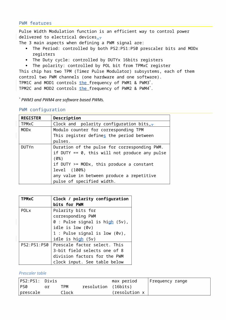
PS2:PS1:PS0 Prescale factor select. This 3-bit field selects one of 8 division factors for the PWM clock input. See table below
Prescaler table
PS2:PS1:PS0prescaler
Divisor TPM resolution max period (16bits)(resolution x MOD)
Frequency range Clock
000 1 16MHz 0,0625 µs 4,10 ms 245Hz – 8MHz001 2 8MHz 0,125 µs 8,19 ms 123Hz – 4MHz010 4 4MHz 0,25 µs 16,38 ms 62Hz – 2MHz011 8 2MHz 0,5 µs 32,77 ms 31Hz – 1MHz 100 16 1MHz 1 µs 65,54 ms 16Hz – 500KHz101 32 500KHz 2 µs 131,07 ms 8Hz – 250KHz110 64 250KHz 4 µs 262,14 ms 4Hz – 125KHz111 128 125KHz 8 µs 524,29 ms 2Hz – 62,5KHz
When a software PWM is activeemployed, the maximum frequency for that TPM is limited to 10Khz.
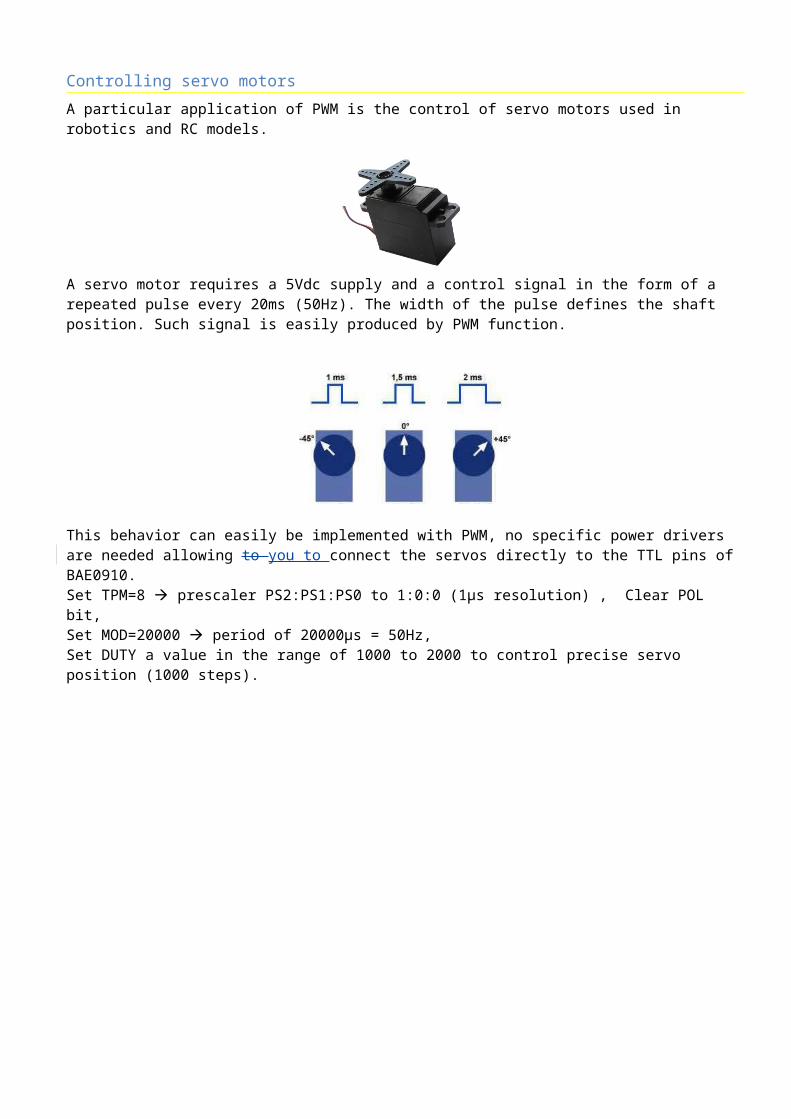
Controlling servo motors
A particular application of PWM is the control of servo motors used in robotics and RC models.
A servo motor requires a 5Vdc supply and a control signal in the form of a repeated pulse every 20ms (50Hz). The width of the pulse defines the shaft position. Such signal is easily produced by PWM function.
This behavior can easily be implemented with PWM, no specific power drivers are needed allowing to you to connect the servos directly to the TTL pins of BAE0910.Set TPM=8 prescaler PS2:PS1:PS0 to 1:0:0 (1µs resolution) , Clear POL bit,Set MOD=20000 period of 20000µs = 50Hz, Set DUTY a value in the range of 1000 to 2000 to control precise servo position (1000 steps).
ADC configuration
This 8 bits ADC is worksing in continuous mode. The various ADC registers are updated in real-time.The analog signal provided to this pin should be in the range 0 to 5V.REGISTER DescriptionADCC ADC configuration bits, see belowADC Instantaneous 8 bits adc sample (read only)ADCAx 16bit read only registers containing last second average for positive and negative samples:
ADCA=ADC x freq / 64ADCTOTx 32 bits Accumulators for every second's averages (Read/ Write registers)
ADCC ADC configuration bitsADCEN ADC/PWM2 selection bit
0 : ADC not active, PWM2 is enabled 1 : ADC is active
OFS Offset control bit0 : Every Ssamples are considered as unsigned and added into ADCAP1 : Samples above 128 are positives, below are negative. (subtract 128) Positives values are accumulated on ADCAPNegatives values are accumulated on ADCAN
GRP Group result control bit.0 : increment ADCTOTx with corresponding ADCAx 1 : increment ADCTOTP with both ADCAx
STP 0 : increment ADCTOTx with ADCAx results1 : Stop accumulation of adc samples in ADCTOTx (ADC and ADCAx still updated)
ADC samples with offset.
Some analog sources need to represent positive and negative values. With a range of 0 to 5V, this is accomplished with adding a 2.5v offset (the middle). In such case, reading 2.5V represents 0, upper values are positives, and lower are negatives.To cope with such representations, the OFS bit on register ADCC control the behavior of average calculation, while the ABS bit control the destination registers used for summations.
ADC averages: ADCAx
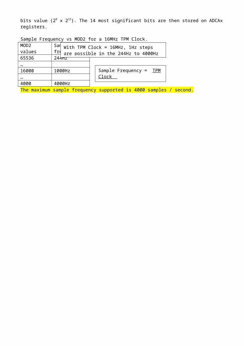
Based on PS2:PS1:PS0 prescaler bits and MOD2 value (see PWM section), you can control time between samples summation. Fine control on the number of samples summed every second allows precise calibration of the averaged value. When a 8bit value is summed at a maximum rate of 4096 Hz, after one second you get an ADC measure that is multiplied by 4096 or 212. This produces a 20 bits value (28 x 212). The 14 most significant bits are then stored on ADCAx registers.
Sample Frequency vs MOD2 for a 16MHz TPM Clock.MOD2 values Sample frequency
65536 244Hz…
16000 1000Hz…
Sample Frequency = TPM Clock MOD2
With TPM Clock = 16MHz, 1Hz steps are possible in the 244Hz to 4000Hz frequency range.
4000 4000HzThe maximum sample frequency supported is 4000 samples / second.
PIO configuration
PIO pin is configurable as INPUT or OUTPUT via PIOC register: PIOC PIO configuration bitsDD Data direction: select INPUT / OUTPUT mode
PE Internal Pull Enable - determines if the internal pull-up or pull-down device is enabled If PIO configured as output, this bit has no effect and the internal pull device is disabled.0 : Internal pull-up/pull-down device disabled 1 : Internal pull-up/pull-down device enabled
PD Pull Down Enable - select a pull-up or pull-down device if enabled.0 : A pull-up device is connected 1 : A pull-down device is connected
DS Output Drive Strength selects between low and high output drive. When configured as input, this bit has no effect.0 : Low output drive strength selected.1 : High output drive strength selected.
PIOEN PIO/PWM4 selection bit0 : normal PIO not active, PWM4 is enabled 1 : normal PIO mode enabled
PIO register read/control PIO pin level.mode PIO PIO data bit (READ/WRITE)input D Read the level present on the PIO pin
0 : less than 0.35 x Vcc volts is present to input pin 1 : more than 0.7 x Vcc is present to input pin
output D Output Data bit 0 : output pin is driven low to GND (sink up to 20mA) 1 : output pin is driven high to Vcc (source up to 20mA)
Writing to an input pin has no effect.Reading an output pin reports the last data written.
COUNTER configuration
COUNTER is configurable via CNTC register to count falling edges or rising edges. CNTC COUNTER configuration bitsPOL Edge select bit
0 : falling edge count.1 : rising edge count.
STP Counter Stop bit0 : counter is incrementing on edge events. 1 : counter stops counting, pin state remains available.
CNT: The lsb of this register reflect the current level present on the pin, writing has no effect.COUNTER: This 32 bits register increments on edge events on the pin, writing this register is allowed.COUNTER pin has no internal pullup/down resistors, external resistor should be added if needed.Warning: the COUNTER pin does not contain a clamp diode to VDD, external Schottky diode is recommended.
RTC configuration
RTC is configurable via RTCC. RTCC RTC configuration bitsSTP RTC stop bit
0 : RTC is incrementing every seconds. 1 : RTC is stopped.
RTC: This 32 bits register increments once every second since last set. On power on sStarts atfrom 0 on power-up.The RTC clock is factory calibrated. The precision is ±0.5%
OUTPUT configuration
OUTPUT pin is configurable via OUTC register to select between OUTPUT/PWM3 mode. OUTC OUTPUT configuration bitsOUTEN OUTPUT/PWM3 selection bit
0 : normal OUTPUT not active, PWM3 is enabled 1 : normal OUTPUT mode enabled
DS Output Drive Strength selects between low and high output drive. 0 : Low output drive strength selected. (4mA)1 : High output drive strength selected. (20mA)
OUT register control the output pin level.OUT OUTPUT data bit (READ/WRITE)D Output Data bit
0 : output pin is driven low to GND (sink up to 20mA) 1 : output pin is driven high to Vcc (source up to 20mA)
ALARM configuration
The state of various alarm conditions is maintained in ALARM register where each bits represents a specific condition. The ALARMC register allows to enablinge corresponding alarm bits.REGISTER DESCRIPTIONALARM See ALARM table for detailsALARMC Alarm configuration bits. Only bits set to 1 will allows to triggerenable response to conditional
search ROM commandALAP Alarm level for positive ADC measure compared with ADCAPALAN Alarm level for negative ADC measure compared with ADCANALCD Alarm level for COUNTER rate exceededALCT Alarm level when COUNTER reached this valueALRT Alarm level when RTC reached this value
ALARM/ ALARMC
ALARM/ ALARMC configuration bits
CT When COUNTER reached a determinedcertain value (ALCT)0 : COUNTER < ALCT 1 : COUNTER >= ALCT This bit is only cleared when the condition is no more longer met.
CR When COUNTER rate per second exceeded a determinedcertain value (ALCD)0 : rate not exceeded 1 : rate exceedThis bit remains set until manually cleared.
AP When ADCAP exceeded a determinedcertain value (ALAP)0 : ADCAP not exceeded 1 : ADCAP exceedThis bit remains set until manually cleared.
AN When ADCAN exceeded a determinedcertain value (ALAN)0 : ADCAN not exceeded 1 : ADCAN exceedThis bit remains set until manually cleared.
PIO When PIO pin state changed 0 : PIO unchanchged 1 : PIO change was detected This bit remains set until manually cleared.
RTC When RTC reached a determinedcertain value (ALRT)0 : RTC < ALRT 1 : RTC >= ALRT This bit is only cleared when the condition is no morelonger met.