Page 1
Development of Antiferromagnetic Heusler Alloys for the Replacement of Iridium as a Critically Raw Material
Atsufumi Hirohata,1 Teodor Huminiuc,2 John Sinclair,2 Haokaifeng Wu,2 Marjan Samiepour,1
Gonzalo Vallejo-Fernandez,2 Kevin O'Grady,2 Jan Balluf,3 Markus Meinert,3 Gunter Reiss,3
Eszter Simon,4 Sergii Khmelevskyi,5 Laszlo Szunyogh,4,6 Rocio Yanes Díaz,7 Ulrich Nowak,7
Tomoki Tsuchiya,8 Tomoko Sugiyama,8 Takahide Kubota,8,9 Koki Takanashi,8,9 Nobuhito
Inami 10 and Kanta Ono 10
1 Department of Electronics, University of York, Heslington, York YO10 5DD, United Kingdom2 Department of Physics, University of York, Heslington, York YO10 5DD, United Kingdom3 Department of Physics, University of Bielefeld, Universitätsstraße 25, 33615 Bielefeld,
Germany4 Department of Theoretical Physics, Budapest University of Technology and Economics,
Budafoki út 8, 1111 Budapest, Hungary5 Center for Computational Materials Science, Institute for Applied Physics, Vienna University
of Technology, Wiedner Hauptstrasse 8, A-1060 Vienna, Austria6 MTA-BME Condensed Matter Research Group, Budapest University of Technology and
Economics, Budafoki út 8., H-1111 Budapest, Hungary7 Department of Physics, University of Konstanz, Postfach 674, 78457 Konstanz, Germany8 Institute for Materials Research, Tohoku University, 2-1-1 Katahira, Sendai 980-8577,
Japan9 Center for Spinctronics Research Network, Tohoku University, 2-1-1 Katahira, Sendai 980-
8577, Japan10 Institute of Materials Structure Science, High Energy Accelerator Research Organization
(KEK), 1-1 Oho, Tsukuba 305-0801, Japan
– 1 –
12
34567
89
101112131415161718192021222324
Page 2
AbstractAs a platinum group metal, iridium (Ir) is the scarcest element on the earth but it has been
widely used as an antiferromagnetic layer in magnetic recording, crucibles and spark plugs
due to its high melting point. In magnetic recording, antiferromagnetic layers have been used
to pin its neighbouring ferromagnetic layer in a spin-valve read head in a hard disk drive for
example. Recently, antiferromagnetic layers have also been found to induce a spin-polarised
electrical current. In these devices, the most commonly used antiferromagnet is an Ir-Mn
alloy because of its corrosion resistance and the reliable magnetic pinning of adjacent
ferromagnetic layers. It is therefore crucial to explore new antiferromagnetic materials without
critical raw materials. In this review, recent research on new antiferromagnetic Heusler
compounds and their exchange interactions along the plane normal is discussed. These new
antiferromagnets are characterised by very sensitive magnetic and electrical measurement
techniques recently developed to determine their characteristic temperatures together with
atomic structural analysis. Mn-based alloys are found to be most promising based on their
robustness against atomic disordering and large pinning strength up to 1.4 kOe, which is
comparable with that for Ir-Mn. The search for new antiferromagnetic films and their
characterisation are useful for further miniaturisation and development of spintronic devices
in a sustainable manner.
– 2 –
252627282930313233343536373839404142
Page 3
I. IntroductionThe European Commission identified 14 critical raw materials (CRMs) in 2011 and revised
to 20 CRMs three years later [1]. These include antimony, beryllium, borates, chromium,
cobalt, coking coal, fluorspar, gallium, germanium, indium, magnesite, magnesium, natural
graphite, niobium, phosphate rock, platinum group metals (PGMs), heavy rare earth
elements, light rare earth elements, silicon metal and tungsten. Similar lists have been made
also by other governments such as those of the USA, Japan and China. As a measure of
criticality, a sustainability index (SI) has been introduced to assess the difficulty in
substituting the material, scored and weighted across all applications. SI values are between
0 and 1, with 1 being the least substitutable. Among these CRMs, phosphate rock has the
highest SI of 0.98, followed by the SIs of chromium, borates, germanium, beryllium and
PGMs of 0.96, 0.88, 0.86, 0.85 and 0.83, respectively. Generally, the PGMs have a relatively
high end-of-life recycling input rate of 35%, which is a measure of the proportion of metal and
metal products that are produced from end-of-life scrap and other metal-bearing low grade
residues in end-of-life scrap worldwide. Even so, among the PGMs, only 1~2% in Pt and Rh
ore contains iridium and 87% of the Ir world supply (~5.8 t in 2011 [2]) is from South Africa.
This makes Ir to be the scarcest element on the earth with the composition of 4×10 -4 ppm,
which is almost one (or more) order of magnitude less than the other PGMs, e.g., Pt (3.7×10-
3 ppm) and Ru (1×10⁻³ ppm).
In general, the PGMs have very high melting point (>1,800K) due to their crystalline
stability. Especially, Ir has one of the highest melting points of 2,739K. Hence, due to its
stability, Ir (and its alloys) has been used as a prototype kilogram, a prototype metre, and for
spark plugs, dip pens, rings and tooth fillings. In addition to these traditional usages,
electrical and electrochemical applications of Ir have been increasing over the last decades,
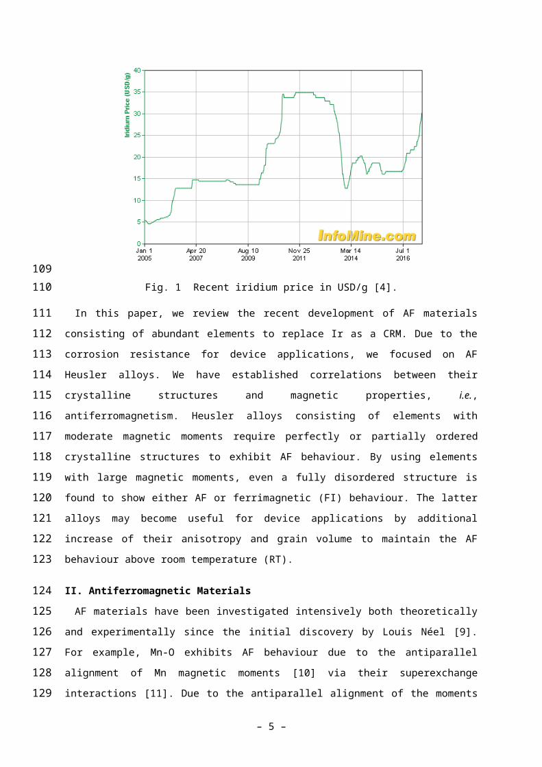
resulting in the worldwide demand of 7.7 t in 2016 [3]. Such a high demand is responsible for
the severe fluctuation in Ir price over the last decade as shown in Fig. 1 [4]. Until the
beginning of 2007, the Ir price was almost stable to be approximately USD 5/g. However, it
took the maximum of USD 35/g in 2011 with over 130% fluctuations. Since the middle of
2016, it has been monotonically increasing again to USD 30/g, approaching the maximum
price. These fluctuations are caused by the above demand greater than the supply and the
associated speculation.
Among the heavy demands, electrical and electrochemical applications are the two major
sectors. For the electrical use (2.1 t worldwide in 2017), antiferromagnetic (AF) Ir-Mn alloys
for magnetic memory and Ir-complex for organic electroluminescence (EL) are major
applications. For organic EL, tridentate [5] and bidentate Ir-complex [6] are used to generate
red, blue, yellow and green EL. To avoid the usage of Ir, carbazolyl dicyanobenzene has
been demonstrated to exhibit EL with these colours with 100% efficiency [7]. For the
– 3 –
43444546474849505152535455565758596061626364656667686970717273747576777879
Page 4
electrochemical use (1.8 t worldwide in 2017), on the other hand, crucibles for sapphire glass
production has been increasing the demands recently due to the sapphire glass usages for
mobile phones and tablet computers. The used crucibles can be recycled by fragmentation of
metal scraps [8]. The metal scraps are dissolved in aqua regia (HNO3+3HCl), followed by the
introduction to PbO solvent and HNO3, NaHSO4 and Na2O2 in series. The residual solution is
then purified as (NH4)3[IrCl6], which can be reduced by H2 gas to Ir. Hence, it is important to
develop a replacement for Ir alloys used in magnetic memory industry, which has no
sustainable solution to date.
Fig. 1 Recent iridium price in USD/g [4].
In this paper, we review the recent development of AF materials consisting of abundant
elements to replace Ir as a CRM. Due to the corrosion resistance for device applications, we
focused on AF Heusler alloys. We have established correlations between their crystalline
structures and magnetic properties, i.e., antiferromagnetism. Heusler alloys consisting of
elements with moderate magnetic moments require perfectly or partially ordered crystalline
structures to exhibit AF behaviour. By using elements with large magnetic moments, even a
fully disordered structure is found to show either AF or ferrimagnetic (FI) behaviour. The
latter alloys may become useful for device applications by additional increase of their
anisotropy and grain volume to maintain the AF behaviour above room temperature (RT).
II. Antiferromagnetic MaterialsAF materials have been investigated intensively both theoretically and experimentally
since the initial discovery by Louis Néel [9]. For example, Mn-O exhibits AF behaviour due to
the antiparallel alignment of Mn magnetic moments [10] via their superexchange interactions
[11]. Due to the antiparallel alignment of the moments with the same amplitude, it is very
– 4 –
8081828384858687
8889909192939495969798
99100101102103
Page 5
difficult to characterise the AF behaviour using macroscopic measurements. Accordingly, a
ferromagnet (FM)/AF bilayer has been introduced to induce interfacial exchange coupling to
pin the magnetisation of the FM layer. This results in a shift in the corresponding
magnetisation curve, which is known as exchange bias field Hex, along a magnetic field
applied [12]. In such a bilayer, the AF properties, e.g., anisotropy and temperature
dependence, can be indirectly characterised by measuring Hex due to the interfacial FM/AF
coupling. From the device application point of view, Hex can pin one of the FM magnetisations
in a FM/non-magnet (NM)/FM trilayer, providing a spin-valve structure [13]. The spin-valve is
a basic building block for a read head of a hard disk drive (HDD), which is the most common
data storage recording almost 85% of the information produced by human being. By
replacing the NM layer with an insulating barrier, a magnetic tunnel junction (MTJ) can also
be fabricated in a similar manner. Such MTJs are used as the latest HDD read head and a
data bit cell of a magnetic random access memory (MRAM). Recently, by flowing an
electrical current in an AF layer, spin polarisation has been demonstrated to be induced,
leading to AF spintronics [14]. For these spintronic applications, an IrMn3 alloy has been
predominantly used due to its corrosion resistance and robustness against device fabrication
processes in nanometre-scale in both thickness and in-plane dimensions (see Table 1 for
major AF materials).
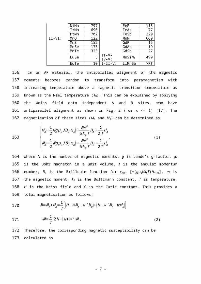
Table 1 List of major AF materials and their Néel temperatures (TN). After Ref. [15],[16].
AF materials TN [K] AF materials TN [K]III-IV: FeO 198 I-VI-III-VI: CuFeO2 11
CoO 291 CuFeS2 825NiO 525 CuFeSe2 70
III: Cr 308 CuFeTe2 254FeMn 493 III-V: FeN 100NiMn 797 FeP 115IrMn 690 FeAs 77PtMn 702 FeSb 220
II-VI: MnO 122 MnN 660MnS 152 GdP 15MnSe 173 GdAs 19MnTe 323 GdSb 27EuSe 5 II-V-IV-V: MnSiN2 490EuTe 10 I-II-V: LiMnSb >RT
In an AF material, the antiparallel alignment of the magnetic moments becomes random to
transform into paramagnetism with increasing temperature above a magnetic transition
temperature as known as the Néel temperature (TN). This can be explained by applying the
Weiss field onto independent A and B sites, who have antiparallel alignment as shown in Fig.
2 (for x << 1) [17]. The magnetisation of these sites (MA and MB) can be determined as
– 5 –
104105106107108109110111112113114115116117118119120121122
123124125126127
Page 6
{MA=12NgμB J BJ (x A )= N m2
6k BTH A=
C2TH A
M B=12NgμB J B J (x B )= N m2
6k BTH B=
C2TH B
, (1)
where N is the number of magnetic moments, g is Lande’s g-factor, µB is the Bohr magneton
in a unit volume, J is the angular momentum number, BJ is the Brillouin function for xA(B)
[=(gµBJ/kBT)HA(B)], m is the magnetic moment, kB is the Boltzmann constant, T is temperature,
H is the Weiss field and C is the Curie constant. This provides a total magnetisation as
follows:
M=M A+M B=CT [ (H−wMA−w' M B )+(H−w ' M A−wMB ) ]
∴M=CT [2H−(w+w ' )M ]. (2)
Therefore, the corresponding magnetic susceptibility can be calculated as
χ=MH
= C
T+C2
(w+w ' )= CT+T N . (3)
Here, w and w’ represent the Weiss field constants within the same site ad across the sites,
respectively. At T=TN, M becomes zero. TN can be determined by measuring the temperature
dependence of magnetic susceptibility. However, for AF thin films, this determination cannot
provide an accurate determination of TN due to their small volumes.
Fig. 2 Schematic AF configuration of magnetic moments.
To characterise an AF material, especially in its thin-film form attached to an FM layer, Hex
has been commonly employed. First, Meiklejohn and Bean assumed a perfect AF/FM
interface with uncompensated interfacial spins to induce exchange coupling but their
calculations were orders of magnitude above measured values. AF domain walls were then
considered at the interface to explain the reduced effective exchange coupling [18].
However, the domain-wall model assumed the rotation of moments along the plane normal,
which cannot explain Hex for a thin AF film with a small moment deviation. Later, Malozemoff
et al. considered the effect of interface roughness on an otherwise compensated AF/FM
interface [19]. The roughness can lead to the formation of AF domains as long as their size is
smaller than the AF grain size. Koon investigated the role of a so-called spin-flop coupling
– 6 –
128
129130131132133
134
135
136
137
138139140141
142143144145146147148149150151152153
Page 7
[20]. However, this coupling alone does not give rise to exchange bias. Defects in the AF,
however, can lead to the formation of AF domains. Model calculations of the so-called
domain-state model show qualitative agreement with many experimental results [21]. A
model which focuses on polycrystalline AF samples was proposed by Fulcomer and Charap
based on the Stoner-Wohlfarth theory [22]. Thermal fluctuations of the grain magnetisation
was taken into account and energy distributions were calculated. By extending the Fulcomer-
Charap model with time (t)-dependence, the York model of exchange bias has been
proposed recently [23].
In polycrystalline films the AF is set below TN to avoid damage to the AF/FM structure. The
AF layer is ordered by the exchange field from the FM layer. This is done by field annealing
using thermal activation giving an ln(t) process. Temperature also causes parts of the AF to
disorder and only the stable grains induce Hex. For Ir-Mn, where TN=690K, the setting of the
AF layer is often incomplete. Using this macroscopic model, temperature dependence of the
magnetisation curves can be reproducibly measured using the York protocol [23]. In the
corresponding York protocol, the AF is set at the setting temperature (TSET) for 90 minutes,
which is above the TN of the AF film but below the Curie temperature (TC) of the FM film. The
sample is then cooled to the thermally activated temperature (TNA). The sample is heated to
the activation temperature (TACT) for 30 mins and is measured at TNA. A period of 30 min
would reverse any activated grains to their original ‘set’ state. These times also negate any
thermal activation that may occur during the temperature rise and fall. This procedure
removes the first loop training effect and measuring at TNA ensures that slow thermal training
does not occur. In polycrystalline systems, individual grains have their own blocking
temperature (TB), which can be determined by increasing the activation temperature until the
loop shift becomes zero. By continuously elevating TNA, TACT becomes TSET, which represents
the median value of TB (<TB>), which is the temperature when the reversed AF volume is
equal to that of the initially set volume. <TB> is an indicative measure of TN.
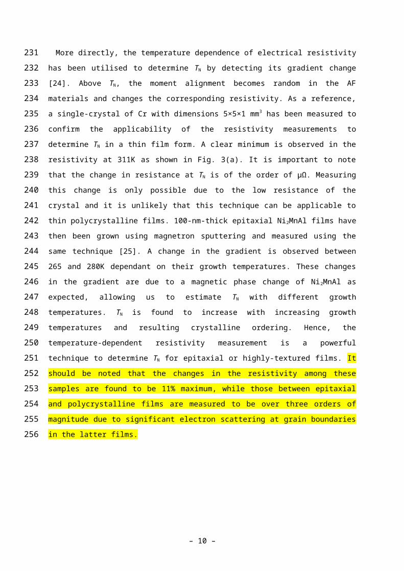
More directly, the temperature dependence of electrical resistivity has been utilised to
determine TN by detecting its gradient change [24]. Above TN, the moment alignment
becomes random in the AF materials and changes the corresponding resistivity. As a
reference, a single-crystal of Cr with dimensions 5×5×1 mm3 has been measured to confirm
the applicability of the resistivity measurements to determine TN in a thin film form. A clear
minimum is observed in the resistivity at 311K as shown in Fig. 3(a). It is important to note
that the change in resistance at TN is of the order of µΩ. Measuring this change is only
possible due to the low resistance of the crystal and it is unlikely that this technique can be
applicable to thin polycrystalline films. 100-nm-thick epitaxial Ni2MnAl films have then been
grown using magnetron sputtering and measured using the same technique [25]. A change
in the gradient is observed between 265 and 280K dependant on their growth temperatures.
– 7 –
154155156157158159160161162163164165166167168169170171172173174175176177178179180181182183184185186187188189190
Page 8
These changes in the gradient are due to a magnetic phase change of Ni2MnAl as expected,
allowing us to estimate TN with different growth temperatures. TN is found to increase with
increasing growth temperatures and resulting crystalline ordering. Hence, the temperature-
dependent resistivity measurement is a powerful technique to determine TN for epitaxial or
highly-textured films. It should be noted that the changes in the resistivity among these
samples are found to be 11% maximum, while those between epitaxial and polycrystalline
films are measured to be over three orders of magnitude due to significant electron scattering
at grain boundaries in the latter films.
Fig. 3 Temperature-dependent resistivity of (a) a single-crystal Cr foil and (b) 100-nm-thick
Ni2MnAl films.
In order to characterise the AF materials microscopically, synchrotron radiation has been
widely employed. X-ray magnetic linear dichroism (XMLD) utilises a pair of linearly polarised
soft X-ray beams with perpendicular polarisation axes, which is different from a pair of
circularly polarised beams used in X-ray magnetic circular dichroism (XMCD) [26], [27]. Here,
XMCD signals are proportional to the average value of a magnetic moment in a domain
(<M>), while XMLD signals are proportional to <M2>. For an AF material, <M> is zero as
MA=–MB within an AF domain in Eq. (2), resulting in no XMCD signal. However, <M2> is a
finite value for an AF material, allowing AF domain imaging. For example for an Fe/NiO
bilayer, NiO domain structures have been observed by taking a Ni L-edge, which is strongly
affected by the exchange coupling between Fe and NiO (spin image), and by taking the O K-
edge, which is originated from the intrinsic AF anisotropy due to the strong coupling with the
Ni 3d orbital (twin image) [28]. For these domain imaging, a large uniform domain (>a few
µm) is required, which makes it difficult to be used for an AF thin films.
Polarised neutron reflectivity (PNR) is another synchrotron-based technique to determine
magnetic properties of bulk and layered materials [29]. Due to the magnetic moment of
neutron beam interacting with magnetic materials to be observed, not only layer structures,
such as thickness, density, composition and interfacial roughness, but also in-plane magnetic
– 8 –
191192193194195196197198
199200201202203204205206207208209210211212213214215216217218
Page 9
moments can be measured. The former structural analysis is similar to X-ray reflectivity
(XRR) measurements but with higher accuracy in a shorter scanning period (<1 min.). The
latter magnetic information can be obtained by detecting the neutron reflection with its spins
interacted with those in an AF and/or FM layers.
In order to develop a replacement for Ir-Mn, RT antiferromagnetism needs to be achieved,
which can be confirmed by the above techniques. To achieve this, three criteria needs to be
satisfied: (i) HEB should be greater than 1 kOe at RT, (ii) <TB> should be above RT and (iii)
the standard deviation of <TB> should be less than 0.3K. As listed in Table 1, however, the
majority of the AF materials have TN near or below RT. Even though some oxides (e.g., NiO)
and sulphides (e.g., CuFeS2) have TN>RT, they have very poor corrosion resistance and
hence cannot be used for the Ir-Mn replacement. Manganese alloys (e.g., NiMn and PtMn)
and nitrides (e.g., MnN and MnSiN2) also have TN>RT. However, NiMn has poor corrosion
resistance and PtMn has very high crystallisation temperature, indicating that they cannot be
used in commercially available devices as replacements for Ir-Mn. Therefore, new AF
Heusler alloys [31], including nitride compounds in their wider definition, need to be
developed for the Ir-Mn replacement.
III. Development of Antiferromagnetic Heusler AlloysA list of major AF and compensated ferrimagnetic (CF) Heusler alloys is shown in Table 2.
The Heusler alloys are categorised into two types: (i) full- and (ii) half-Heusler alloys. These
alloys crystallise in (i) L21 phase with X2YZ composition and (ii) C1b phase with XYZ
composition as shown in Fig. 4, respectively [50]. The half-Heusler alloys have an X-vacancy
in the unit cell, making it to be susceptible to atomic displacement. Even for the full-Heusler
alloys, the perfectly-ordered L21 phase can be deformed into the B2 phase by atomically
displacing Y-Z elements, the D03 phase by X-Y displacements and the A2 phase by
randomly exchanging X-Y-Z elements. The degree of crystallisation in the full-Heusler alloy
films can be quantified based on the intensity and width of the (220) principal peaks in X-ray
or electron-beam diffraction, indicating the formation of the A2 phase. The coexistence of
both the (220) and (200) peaks can indicate the formation of the B2 crystalline ordering. The
existence of the additional (111) peak confirms some degree of the formation of the perfectly
ordered L21 crystalline phase.
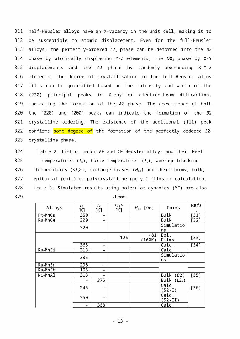
Table 2 List of major AF and CF Heusler alloys and their Néel temperatures (TN), Curie
temperatures (TC), average blocking temperatures (<TB>), exchange biases (Hex) and their
forms, bulk, epitaxial (epi.) or polycrystalline (poly.) films or calculations (calc.). Simulated
results using molecular dynamics (MF) are also shown.
Alloys TN [K] TC [K] <TB> [K] Hex [Oe] Forms Refs.Pt2MnGa 350 – Bulk [31]
– 9 –
219220221222223224225226227228229230231232233234
235236237238239240241242243244245246247248249250251252
Page 10
Ru2MnGe 300 – Bulk [32]320 Simulations
– 126 >81 (100K) Epi. Films [33]365 – Calc. [34]
Ru2MnSi 313 – Calc.335 Simulations
Ru2MnSn 296 –Ru2MnSb 195 –Ni2MnAl 313 – Bulk (B2) [35]
– 375 Bulk (L21)245 – Calc. (B2-I) [36]350 – Calc. (B2-II)
– 368 Calc. (L21)340372 – Calc. (B2-I)
MF Calc. [37]
220352 – Calc. (B2-II)
MF Calc.285 – Calc. (B2-II)310 – >55 (10K) Epi. Films [25]
Mn2VAl >600 – Bulk [38]
>RT – ~200 120 (4K)20 (RT) Epi. Films
360636 – Calc.
MF Calc.Mn2VSi – <100 34 (100K) Poly. Films [39]Mn3Ga 470 – Bulk [40]
648 – ~400 1.5k (RT) Epi. Films [41]– 235 430 (120K) Poly. Films [42]
Mn3.04Ge0.96 390 [43][44]
Mn2.4Pt0.6Ga – ~90 33k (2K)0 (90K) Bulk [45]
Mn1.8FeGa – ~350 12k (2K)~300 (RT) Bulk
Mn2.5Co0.3Ga1.2 – >350 250 (RT) Poly. filmsMnN 660 – 388 1475 (RT) Poly. Films [46]
570 – Calc.Fe2VAl Calc. [47]
Poly. films [48]Cr2MnSb 342 Calc. [49]
As shown in Fig. 5, the Heusler alloys can be formed with the X and Y atoms to be
transition metals and the Z atom to be a semiconductor or a non-magnetic metal. These
combinations provide more than 2,500 Heusler alloys. In addition, constituent elements in a
Heusler alloy can be substituted by the other elements, offering great opportunity for the
development of a new AF material [51]. In particular, by counting the total number of valence
electrons, the atomic substitution is known to maintain the corresponding magnetic
properties to satisfy the generalised Slater-Pauling curve. This allows the continuous
engineering of the AF properties in the Heusler alloys with controlling their lattice constants
and associated crystalline anisotropy.
– 10 –
253254255256257258259260261
Page 11
Fig. 4 Crystalline ordering of Heusler alloys: (a) half-Heusler alloy with the C1b phase and
full-Heusler alloy with the (b) L21, (c) B2 and (d) A2 phases [48].
Fig. 5 Major combinations of Heusler alloys [50].
In Heusler alloys, half-Heusler alloys have low Néel temperatures in general. For example,
CuMnSb [52], NdBiFe [53] and GdPdBi [54] have their TN to be 55, 2.18 and 13K,
respectively. These are not suitable for Ir-Mn replacement in spintronic devices due to their
low TN<RT and due to the use of rare materials in the latter two alloys. Therefore, full-Heusler
alloys have been focused for the development of AF films with their TN>RT.
As listed in Table 2, Fe2VAl, where Y and Z elements can be substituted with any other
elements as listed in Fig. 5, has been predicted to have a tendency to form a spin-glass
(form AF ordering in Fe2.5V0.5Al) [47]. Mn2VAl is analogous to Fe2VAl but replaces the Fe with
the very high moment Mn. These alloys can be further engineered by substituting some of
Mn atoms with the other high-moment atoms to form (Co,Mn)2VAl for instance, which is
analogous to the other two families with the exception that the element denoted X is now
replaced by a mixture of two high moment atoms. By replacing V with Mn, low-moment-
based alloys, e.g., Ni2MnAl, are anticipated to have a high compensated moment. By utilising
a heavier element as a base of the Heusler alloys, Ru2MnAl is expected to have the potential
– 11 –
262263264
265266267268269270271272273274275276277278279280
Page 12
advantage of having both X and Y as the high moment atoms. These families are anticipated
to exhibit AF ordering. For RT antiferromagnetism, the AF phase should be stabilised by
introducing larger anisotropy and larger AF grain volume. Recently, perpendicularly
magnetised FM has also been reported to be pinned by IrMn layer [55]. Hence, the
introduction of the additional tetragonal distortion into the cubic Heusler alloys may be
necessary for the development of a RT AF.
1. Ru-based Heusler alloysEpitaxially grown Ru2MnGe films have a very small lattice mismatch of 0.5% on a
MgO(001) substrate with the relationship, Ru2MnGe[100](001) || MgO[110](001)
(aRu2MnGe=0.5985 nm and aMgO=0.5957 nm). At a substrate temperature Tsub>400°C, the
formation of epitaxial films has been reported [33]. The optimum growth temperature has
been reported to be Tsub=500°C, where the diffraction peaks and their Laue oscillations are
most pronounced. At higher temperatures, Mn starts to evaporate from the sample. The
calculated lattice constant deduced from the (200) and (400) peak positions in X-ray
diffraction (XRD) measurements is c=0.6041 nm. Considering a 1% tetragonal distortion
induced by the compressive strain from the lattice mismatch, the lattice constant matches the
prediction if the unit cell volume is held constant.
Figure 6 shows a series of hysteresis loops for a sample with an epitaxial Ru2MnGe/Fe
bilayer measured following the same experimental procedure as used for a granular AF/FM
system [23]. As can be seen, progressive thermal activation leads to a reversal of the
exchange bias as shown in Figure 6(a). This allows for the distribution of TB to be calculated
as shown by the line in Figure 6(b), showing <TB>=126K.
Fig. 6 (a) Hysteresis loops showing the reversal of exchange bias of Ru2MnGe/Fe sample.
(b) Hex obtained for Ru2MnGe in a reversed cooling experiment as a function of temperature.
The optimum epitaxial Ru2MnGe/Fe bilayers have been imaged using cross-sectional
transmission electron microscopy (TEM). Both substrate and FM layer interfaces confirm the
lattice matching and crystalline quality. The thin FM layer does not offer enough contrast for
– 12 –
281282283284285286287288289290291292293294295296297298299300301302
303304305306307308
Page 13
TEM studies. The (220) and (200) reflections are observed for the (110) Heusler zone axis.
The (222) reflections indicate the formation of the L21 phase.
Fig. 7 Cross-sectional TEM images of epitaxial Ru2MnGe/Fe layers with the corresponding
selected area electron diffraction (SAED) pattern.
The magnetic state and its dependence on the atomic disorder and chemical composition
for Ru2MnGe have been investigated within a multi-scale approach [56] combining first
principles calculations with advanced classical spin model simulations. Based on the first
principles calculations, spin models were first parameterised and then, in a second step
simulated by means of the stochastic Landau-Lifshitz-Gilbert equation of motion. Hysteretic
as well as thermal properties of bilayers of Ru2MnZ/Fe (Z = Si or Ge) can thus be obtained.
The Ru-based bilayers show exchange bias in agreement with above measurements. This
effect is much stronger than in the Ni-based bilayers as discussed in the following sub-
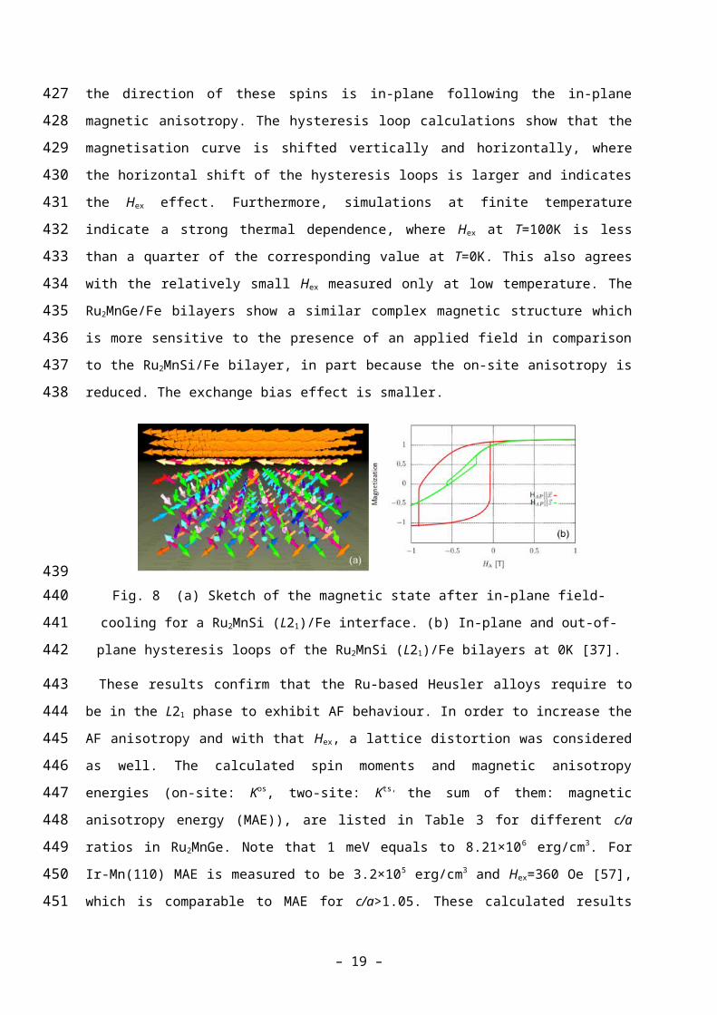
section. As Figure 8 illustrates for a Ru2MnSi/Fe interface, exchange bias exists without
structural disorder in the antiferromagnet, i.e., for the L21 phase. Due to the strong FM
coupling between the interface atoms, close to the interface, the Fe and Mn spins are
oriented nearly parallel, and the direction of these spins is in-plane following the in-plane
magnetic anisotropy. The hysteresis loop calculations show that the magnetisation curve is
shifted vertically and horizontally, where the horizontal shift of the hysteresis loops is larger
and indicates the Hex effect. Furthermore, simulations at finite temperature indicate a strong
thermal dependence, where Hex at T=100K is less than a quarter of the corresponding value
at T=0K. This also agrees with the relatively small Hex measured only at low temperature.
The Ru2MnGe/Fe bilayers show a similar complex magnetic structure which is more sensitive
– 13 –
309310
311312313314315316317318319320321322323324325326327328329330331
Page 14
to the presence of an applied field in comparison to the Ru2MnSi/Fe bilayer, in part because
the on-site anisotropy is reduced. The exchange bias effect is smaller.
Fig. 8 (a) Sketch of the magnetic state after in-plane field-cooling for a Ru2MnSi (L21)/Fe
interface. (b) In-plane and out-of-plane hysteresis loops of the Ru2MnSi (L21)/Fe bilayers at
0K [37].
These results confirm that the Ru-based Heusler alloys require to be in the L21 phase to
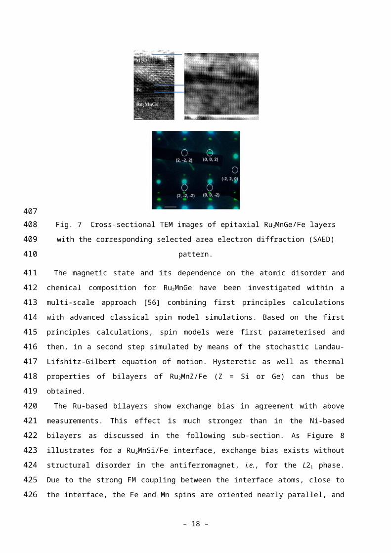
exhibit AF behaviour. In order to increase the AF anisotropy and with that Hex, a lattice
distortion was considered as well. The calculated spin moments and magnetic anisotropy
energies (on-site: Kos, two-site: Kts, the sum of them: magnetic anisotropy energy (MAE)), are
listed in Table 3 for different c/a ratios in Ru2MnGe. Note that 1 meV equals to 8.21×10⁶
erg/cm3. For Ir-Mn(110) MAE is measured to be 3.2×10⁵ erg/cm3 and Hex=360 Oe [57], which
is comparable to MAE for c/a>1.05. These calculated results suggest that tetragonal
distortion (stretching) induces large uniaxial anisotropy in Ru2MnZ due to a combined effect
of symmetry breaking and spin-orbit coupling. It should be noted that a similar AF behaviour
has been reported for the other heavy-metal-based Heusler alloys, such as Pt2MnGa [31].
Therefore, for the heavy-metal-based Heusler alloys, high-moment element, e.g., Mn, is
necessary to induce AF behaviour. The AF anisotropy can be increased by introducing
tetragonal distortion, leading to RT AF behaviour.
Table 3 Calculated magnetic moments (mMn), Kos, Kts and MAE for Ru2MnGe with tetragonal
lattice distortion.
mMn [mB] Kos [meV] Kts [meV] MAE=Kos+Kts
[meV]c/a=1.00 2.91 9.7 ´ 10-5 -2.7 ´ 10-4 -1.8 ´ 10-4
c/a=1.05 2.88 0.32 0.21 0.53c/a=1.10 2.79 0.54 0.41 0.95c/a=1.15 2.65 0.55 0.82 1.37c/a=1.20 2.49 0.43 0.80 1.23
2. Ni-based Heusler alloysNi2MnAl films grown on MgO(001) exhibit the superlattice (200) diffraction but no (111)
peak in addition to the fundamental (220) diffraction using XRD, which suggests that the films
– 14 –
332333
334335336337338339340341342343344345346347348349350351352
353354355
Page 15
are in the B2 phase [25]. The results of XRD φ-scans confirm that all films including the film
deposited at RT satisfy the epitaxial relation, Ni2MnAl[100](001) || MgO [110](001). Hex of 55
Oe is obtained for the RT grown films, while no exchange bias (rather a weak FM signals) is
detected for those grown at higher temperatures, e.g., 600ºC as shown in Fig. 9.
Fig. 9 Hysteresis loops showing the reversal of exchange bias of Ni2MnAl/Fe sample grown
at (a) RT and (b) 600ºC. (c) Hex obtained for Ni2MnAl in a reversed cooling experiment as a
function of temperature [25].
To identify the differences between these Ni2MnAl layers grown at RT and 600ºC, the
Ni2MnAl epitaxial samples have been imaged using cross-sectional TEM. The epitaxially
deposited Ni2MnAl/Fe bilayers exhibit good crystalline structure as seen in Fig. 10 with sharp
interfaces which may exhibit less than three atomic planes in roughness. Here, the Ni2MnAl
films grown at 600ºC are found to form the L21 phase confirmed by the presence of the (111)
diffraction spots in their SAED image in Fig. 10. However, those grown at RT form the B2
phase without the (111) spots but with the (220) and (200) spots. By taking the above
magnetisation measurements, Ni2MnAl requires the B2 ordering to exhibit AF behaviour. The
Ni2MnAl layer shows a number of crystalline defects that define a fine granular-like structure
due to the local breaking of symmetry within the atomic planes. The random distribution of
crystalline boundaries may be detrimental to the thermal stability of AF, as the formation of
small single domain structures of around 5 nm or less may lead to thermal instability of the
material. A larger grain size and columnar growth are more desirable for increased thermal
stability of the AF structure.
– 15 –
356357358359
360361362363364365366367368369370371372373374375376377
Page 16
Fig. 10 Cross-sectional TEM images of epitaxial Ni2MnAl/Fe layers grown at (a) RT and (b)
600ºC with the corresponding SAED patterns.
In the case of the Ni-based AF in the crystallographically ordered L21 phase, the atomistic
calculations confirm that no exchange bias occurs [58]. However, in that case a spin-flop
coupling can lead to an enhanced coercivity and to the fact that one can switch the AF with
an external field via the coupling to FM. For the partially disordered B2 phase of the Ni2MnAl,
a small Hex has been found as shown in Fig. 11, which agrees with experiments as described
above. The reason for the exchange bias effect is a combination of the disorder, which leads
to uncompensated spin structures along the interface, with the anisotropy of AF. MAE has
been calculated along the path between the ordered B2-I and B2-II structures as a function
of Mn concentration on the Al sites (see Fig. 12). This confirms that short-range order can
induce sizeable MAE for B2-II. Since the anisotropy is rather low (an order of magnitude
smaller than that for the Ru-based Heusler alloys), Hex is rather small, and depends on the
grain volume. It is furthermore rather unstable against thermal fluctuations with a maximum
TB of below 100K as agreed with the experiment. In order to investigate a potential increase
of Hex through a lattice distortion the MAE per unit cell has been calculated for several values
of the c/a ratio in the B2 phase (see Table 4). Therefore, the Heusler alloys based with a
transition metal with a small magnetic moment exhibits their AF phase when the high-
moment Y atoms form antiparallel configuration between their second-nearest neighbours.
– 16 –
378379380381382383384385386387388389390391392393394395396397
Page 17
Fig. 11 (a) Sketch of the magnetic state after field-cooling for a Ni2MnAl (B2-II)/Fe interface.
(b) In-plane hysteresis loops of the Ni2MnAl (B2)/Fe bilayers at T=0; 20 and 100 K [58].
Fig. 12 MAE as a function of Mn concentrations in Ni2MnAl and the corresponding crystalline
structures.
Table 4 Calculated MAE for Ni2MnAl with tetragonal lattice distortion.
c/a=0.90 c/a=0.95 c/a=1.00 c/a=1.05 c/a=1.10MAE [meV] 0.054 0.027 0.00 -0.028 -0.059
3. Mn-based Heusler alloysAs a Heusler alloy based with a transition metal with a high moment, Mn2VAl films have
been grown onto MgO(001) single crystalline substrates. The superlattice diffraction of the
(200) peak appears for the growth temperatures, Tsub=500ºC and 600ºC. In addition, these
samples exhibit the (111) superlattice diffraction in a pseudo-in-plane scan. These results
indicate that the films are in the L21 phase for Tsub≥500ºC. On the other hand, only the
fundamental (400) diffraction appears for the other samples with Tsub≤400ºC, suggesting that
the films are in the A2 phase. SAED patterns are shown in Fig. 13 for Tsub = 400ºC and
600ºC representing the A2 phase and L21 phase, respectively.
Figure 13 shows the Tsub dependence of magnetisation values for Mn2VAl films measured
at RT. The films exhibit saturation magnetisations of 190 and 220 emu/cm3 for Tsub=500ºC
and 600ºC, respectively. On the other hand, no FM (or FI) magnetic hysteresis loop appears
for the other samples with the A2 phase, which suggests a possibility to be an AF or CF. The
Tsub dependence of the chemical phases and magnetization values are similar with those
– 17 –
398399400
401402403404
405406407408409410411412413414415416417418
Page 18
reported in a previous work [59]. By depositing the optimised Mn2VAl/Fe bilayer, Hex of 120
Oe at 10K has been measured [38], which decreases rapidly with increasing temperature but
is maintained to be ~10 Oe at 200K. The corresponding <TB> has been estimated to be ~75K
using the York protocol.
Fig. 13 SAED patterns of Mn2VAl films. (a) Tsub=400ºC and (b) 600ºC.
PNR experiments has confirmed the presence of an AF phase at RT in a polycrystalline
A2-ordered Mn2VAl bulk sample. The Mn2VAl sample show an AF peak at the (100) reflection
of the A2 phase which disappears at around 500K on top of a broad nuclear reflection peak
from the L21 phase [60]. From another set of neutron diffraction experiments on Mn2VAl
epitaxial films, the film deposited at 400ºC is found to show AF A2 phase at RT, while those
deposited at room temperature and 600ºC show A2 phase without AF ordering and L21
phase, respectively [38]. The corresponding magnetisation values as shown in Fig. 14
confirms the crystallisation of the AF (the growth temperature (Tsub)<400ºC) and FI
(Tsub>400ºC).
Fig. 14 Substrate temperature, Tsub dependence of saturation magnetisation, Ms for Mn2VAl
films.
The ordered Mn2VAl alloy has a FI ground state with rather large V moments oriented
opposite to the Mn moments. Here the strong antiparallel Mn-V couplings stabilise the FI
state. In order to trace the effect of atomic disorder in the system, the B2 phase is calculated
as shown in Fig. 15. Here, the AF coupling between in-plane first nearest neighbour Mn
atoms is much weaker than those between out-of-plane Mn atoms, indicating the presence of
– 18 –
419420421422
423424425426427428429430431432433
434435436437438439440441
Page 19
out-of-plane anisotropy. The disorder between the V and Al atoms does not influence
significantly the magnetic state as compared to the ordered L21 state. The fully disordered A2
phase is also studied as a random three-component alloy in terms of single site coherent
potential approximation (CPA). The completely disordered A2 state is calculated to be non-
magnetic at the same lattice constant as for the L21 phase. Only by increasing the lattice
parameter by more than 8% a spontaneous FM state has been formed. The failure of
obtaining an AF ground state (in fact, a magnetic ground state) at the experimental lattice
constant indicates that magnetism collapses when a homogeneous atomic disorder is
supposed like with the CPA and, most possibly, atomic short-range order (e.g., clustering of
Mn atoms) would stabilise the magnetic order in the system.
Fig. 15 (a) Sketch of the magnetic ground state of Mn2VAl (L21) bulk. (b) Calculated Mn-Mn
and Mn-V exchange parameters for Mn2VAl as a function of the inter-atomic distance for the
ordered L21 and the partially disordered B2 phases.
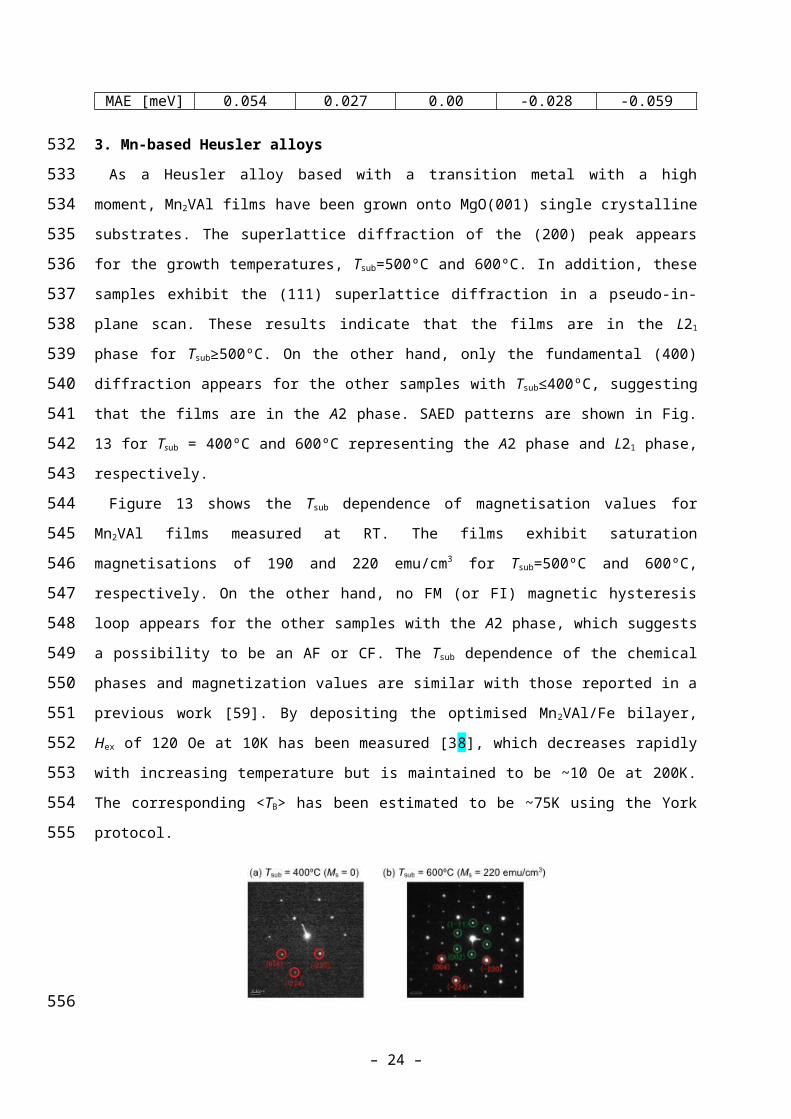
For the Mn-based Heusler alloys, off-stoichiometric compositions have also been
investigated, which confirms the robustness of the Mn-based alloys against their atomic
disorder. By taking two FI Heusler alloys, Mn3Ga and Mn2PtGa, their compensation point,
Mn2.4Pt0.6Ga, has been calculated and demonstrated experimentally [45]. As shown in Fig.
16(a), a local FM domain can be exchange biased by a neighbouring AF domain within such
compensated FI, inducing Hex of 33 kOe at 2K. In a similar system of Mn1.8FeGa, Hex is
reported to survive to be ~300 Oe up to RT [see Fig. 16(b)].
– 19 –
442443444445446447448449450451
452453454455456457458459460461462
Page 20
Fig. 16 (a) Temperature dependence of Hex for Mn2.4Pt0.6Ga and Mn2.5Pt0.5Ga. The inset
shows the coercive field HC and Hex as a function of the Pt concentration x in Mn3-xPtxGa. (b)
Temperature dependence of Hex for Mn1.5Fe1.5Ga and Mn1.8FeGa. The lines are guides to the
eye [45].
By further substituting Y elements with Mn, binary Heusler alloys can be formed. One
example is hexagonal Mn3Ge [44]. Hex of up to 520 Oe is measured at the boundaries
between AF and FM domains as shown in Fig. 17. Similar off-stoichiometric AF Heusler
alloys are reported as Fe2VAl and Cr2MnSb. Even though these results may not be directly
compared with those for the AF/FM bilayers, these alloys may be used as new AF layers. A
tetragonal Mn3Ga film has then been investigated to induce AF behaviour [40]. A bilayer of
epitaxial Mn3Ga (10 nm)/Co0.9Fe0.1 (2.5 nm) is reported to show Hex of 1.5 kOe at RT. MAE
and <TB> are estimated to be 3×10⁶ erg/cm3 and ~400K, respectively. Recently, Hex of 430
Oe at 120K in polycrystalline Mn3Ga/Co0.6Fe0.4 bilayers, confirming the applicability of such
binary Heusler alloys for the replacement of Ir-Mn.
– 20 –
463464465466467468469470471472473474475476477
478
Page 21
Fig. 17 Variation of Hex with number of field cycles n measured at 2K. The line serves as a
guide to the eye. The inset shows the training effect on the M(H) loops [44].
By further expanding the definition of the Heusler alloys to nitrides [32], MnN has been
investigated. MnN films are grown using ultrahigh vacuum sputtering in N2 atmosphere to
achieve Mn:N=1:1. A MnN/Fe bilayer has been reported to show Hex of 1.4 kOe at RT with
<TB>=388K as shown in Fig. 18 [46]. This satisfies the requirements for the Ir-Mn
replacement. However, the minimum thickness of MnN to induce the AF behaviour is 20 nm,
which needs to be at least halved to be competitive against the 6-nm-thick Ir-Mn layer used
in spintronic devices.
Fig. 18 (a) Hysteresis loops showing the reversal of exchange bias of MnN/Fe sample. (b)
Hex obtained for MnN in a reversed cooling experiment as a function of temperature.
Therefore, high-moment-metal-based Heusler alloys display AF behaviour possibly due to
the clustering of the high-moment metals even in their disordered A2 phase. MAE is
demonstrated to be increased by introducing tetragonal distortion into the unit cell of the
alloys. Further engineering in distortion and AF domain size can increase <TB> and Hex of
these alloys, allowing the replacement for Ir-Mn alloys used in spintronic devices.
IV. ConclusionRu2YZ, Ni2YZ and Mn2YZ Heusler alloys have been found to exhibit AF behaviour in their
L21, B2 and A2 crystalline ordering phases. By attaching a FM Fe layer to these AF layers,
Hex of up to 600 Oe at 100K, 90 Oe at 100K and 30 Oe at 100K for Ru2MnGe, Ni2MnAl and
Mn2VAl, respectively. Mn2VAl is found to maintain its AF properties at RT. These differences
are found to be induced by the AF alignment of spin moments at the Y site in unique ordering
phases. In the ordered L21 type Ru2MnZ (Z = Si, Ge, Sn or Sb), the complex AF ordering
(2nd type) is a consequence of the frustrated exchange interaction between the Mn atoms. It
is concluded that TN sharply depends on the Z element and that TN in Ru2MnGe can be
increased by avoiding the disorder in the Mn-Z sub-lattice. For Ni2MnAl, the (checkerboard-
– 21 –
479480481482483484485486487
488489490491492493494495
496497498499500501502503504505
Page 22
like) AF order only exists in the chemically disordered B2 phase due to the large AF nearest
neighbour Mn-Mn interaction. Decreasing the atomic disorder in the Mn-Al sublattice leads to
non-zero total magnetisation (ferrimagnet). Moreover, the excess of Mn or Ni does not
improve the quality of the AF state. From the device application point of view, Mn-based AF
Heusler alloys are ideal due to their robustness against atomic disordering, especially at the
interfaces against their neighbouring layers. These findings are useful for future
implementation to replace iridium alloys in spintronic devices from their sustainability points
of view.
AcknowledgementsThe authors would like to thank Dr Asaya Fujita of AIST for fruitful discussion. This work
was part-funded through a project, HARFIR (Heusler alloy replacement for Iridium), by the
European Commission under the 7th Framework Programme (FP7-NMP-2013-EU-Japan,
Grant Agreement No: NMP3-SL-2013-604398) and by the Japan Science and Technology
Agency through its Strategic International Collaborative Research Program. A.H, G.V.F. and
K.O.G. would also like to thank financial support from the UK EPSRC (EP/M02458X/1), while
E.S. and L.S. acknowledges the support of the National Research, Development and
Innovation Office of Hungary (Project No. K115575).
References[1] 2014 Communication on the review of the list of critical raw materials for the EU and the
implementation of the Raw Materials Initiative (https://ec.europa.eu/growth/sectors/raw-
materials/specific-interest/critical_en).
[2] http://www.matthey.com/
[3] http://www.platinum.matthey.com/documents/new-item/pgm%20market%20reports/
pgm-market-report-may-2016.pdf
[4] http://www.infomine.com/investment/metal-prices/iridium/all/
[5] M. A. Baldo et al., Appl. Phys. Lett. 75, 4 (1999).
[6] H. Konno, Tech. Chem. Times, 199, 13 (2006).
[7] H. Uoyama et al., Nature 492, 234 (2012).
[8] Sumitomo Mining, Japanese Patent (2010-132144).
[9] L. Néel, Annales de Physique 3, 137 (1948).
[10] C. G. Shull and J. S. Smart, Phys. Rev. 76, 1256 (1949).
[11] P. W. Anderson, Phys. Rev. 79, 350 (1950).
[12] W. H. Meiklejohn and C. P. Bean, Phys. Rev. 105, 904 (1957).
[13] R. E. Fontana, Jr. et al., US Patent 5,701,223 (1997).
[14] T. Jungwirth et al., Nature Nanotech. 11, 231 (2016).
[15] T. Jungwirth et al., Phys. Rev. B 83, 035321 (2011).
– 22 –
506507508509510511512513
514515516517518519520521522
523524525526527528529530531532533534535536537538539540541
Page 23
[16] F. Máca et al., J. Magn. Magn. Mater. 324, 1606 (2012).
[17] S. Chikazumi, Physics of Ferromagnetism (Clarendon Press, Oxford, 1997), pp. 134-
159.
[18] D. Mauri et al., J. Appl. Phys. 62, 3047 (1987).
[19] A. P. Malozemoff, Phys. Rev. B 35, 3679 (1987); ibid. 37, 7673 (1988).
[20] N.C. Koon, Phys. Rev. Lett. 78, 4865 (1997).
[21] U. Nowak et al., Phys. Rev. B 66, 014430 (2002).
[22] E. Fulcomer and S. H. Charap, J. Appl. Phys. 43, 4190 (1972).
[23] K. O'Grady et al., J. Magn. Magn. Mater. 322, 883 (2010).
[24] K. Fukamichi, Antiferromagnets (Kyoritsu, Tokyo, 2014).
[25] T. Tsuchiya et al., J. Phys. D: Appl. Phys. 49, 235001 (2016).
[26] B. T. Thole et al., Phys. Rev. Lett. 55, 2086 (1985).
[27] D. Alders et al., Phys. Rev. B 57, 11623 (1998).
[28] T. Kinoshita et al., J. Phys. Soc. Jpn. 73, 2932 (2004).
[29] J. A. C. Bland and B. Heinrich (Eds.), Ultrathin Magnetic Structures I (Springer, Berlin,
1994), pp. 305-343.
[30] S. Singh et al., Nature Commun. 7, 12671 (2016).
[31] J. Kubler, private communications.
[32] S. Mizusaki et al., J. Alloys Comp. 510, 141 (2012).
[33] J. Balluff et al., J. Appl. Phys. 118, 243907 (2016).
[34] S. Khmelevskyi et al., Phys. Rev. B 91, 094432 (2015).
[35] M. Acet et al., J. Appl. Phys. 92, 3867 (2002).
[36] I. Galanakis et al., Appl. Phys. Lett. 98, 102514 (2011).
[37] R. Yanes Díaz et al., private communications.
[38] T. Tsuchiya et al., http://arxiv.org/abs/1707.06731.
[39] H. Wu et al., J. Phys. D: Appl. Phys. (in press).
[40] E. Krén and G. Kádár, Solid State Commun. 8, 1653 (1970).
[41] H. Kurt et al., Appl. Phys. Lett. 101, 232402 (2012).
[42] H. Wu et al., Appl. Phys. Lett. Mater. (submitted).
[43] G. Kadar and E. Kren, Int. J. Magn. 1, 143 (1971).
[44] J. F. Quian et al., J. Phys. D: Appl. Phys. 47, 305001 (2014).
[45] A. K. Nayak et al., Nature Mater. 14, 679 (2015).
[46] M. Meinert et al., Phys. Rev. B 92, 144408 (2015).
[47] D. J. Singh and I. Mazin, Phys. Rev. B 57, 14352 (1998).
[48] T. Huminiuc et al. (in preparation).
[49] I. Galanakis et al., Phys. Rev. B 75, 172404 (2007).
[50] A. Hirohata et al., Curr. Opin. Solid State Mater Sci. 10, 93 (2006).
– 23 –
542543544545546547548549550551552553554555556557558559560561562563564565566567568569570571572573574575576577578
Page 24
[51] C. Felser and A. Hirohata (Eds.), Heusler Alloys (Springer, Berlin, 2016).
[52] K. Endo, J. Phys. Soc. Jpn. 29, 643 (1970).
[53] R. A. Muller et al., Phys. Rev. B 92, 184432 (2015).
[54] C. B. R. Jesus et al., Solid State Commun. 177, 95 (2014).
[55] J. Y. Chen et al., Appl. Phys. Lett. 104, 152405 (2014).
[56] R. Yanes Díaz et al., Phys. Rev. Lett. 111, 217202 (2013).
[57] M. Takanashi and M. Tsunoda, J. Phys. D: Appl. Phys. 35, 2365 (2002).
[58] R. Yanes Díaz et al., Phys. Rev. B (under review), http://arxiv.org/abs/1707.08651.
[59] T. Kubota et al., Appl. Phys. Lett. 95, 222503 (2009).
[60] R. Y. Umetsu, private communications.
– 24 –
579580581582583584585586587588