13
Packaging Design Rules for Si- & InP- Photonics DRAFT 1.0 – March 2015

Packaging Design Rulesfor Si- & InP-Photonics
DRAFT 1.0 – March 2015
Please return comments directly in the document using the track changes function before 3 April 2015 to [email protected]

Index
1 - Introduction Page 2
2 - General Considerations Page 22.1 Orientation of PIC for Packaging Page 22.2 Electrical Connections to PIC Page 32.3 Thermal Effects for PIC Page 4
3 - Grating-Coupling: Si-Photonics Page 43.1 Grating Couplers Page 43.2 Coupling to Fibre-Arrays Page 53.3 Extension to InP-Photonics Page 6
4 - Edge-Coupling: InP-Photonics Page 64.1 Edge Couplers Page 64.2 Coupling to Fibre-Arrays Page 74.3 Extension to Si-Photonics Page 7
5 - Conclusion & Contacts Page 7
EPIC – Packaging Design Rules for Si- & InP-Photonics – March 2015 P a g e | 1
1 IntroductionPhotonic packaging covers the optical- and electronic-coupling of photonic integrated circuits (PICs) to the outside world. To help ensure that PICs can be packaged efficiently and reproducibly, it is important to follow the basic packaging design rules and standards (PDRs) outlined in this document, and the specific (stricter) PDRs from individual packaging suppliers. These PDRs specify the recommended dimensions and locations of the optical and electronic ports of the PIC, with respect to physical footprint of the PIC-die, as well as offering best-practice design suggestions that help streamline the packaging process. If the PDRs are not followed, then packaging may be difficult, or even physically impossible.
The PDRs cover the packaging of Si-, InP-, and TriPleX-photonic integrated circuits. Very broadly speaking, Si-Photonics allows for photonic-integration directly with CMOS-compatible electronics, while InP-Photonics allows for the combination of both active and passive photonic components on a single-chip. TriPleX allows for passive photonics circuits covering a broader wavelength range (300nm-1900nm) than is possible with either Si- or InP-Photonics. The PDRs are divided into three sections - (i) general considerations for packaging PICs, irrespective of their material-platform, including orientation, electrical connections, and thermal management, (ii) grating-coupling for optical-coupling to Si-PICs, (iii) edge-Coupling for optical-coupling to InP- and TriPleX-PICs.
2 General ConsiderationsCertain photonic-packaging considerations are independent of material platform, i.e. they are equally applicable to Si-, InP-, and TriPleX-PICs. For example, the bond-pads needed for electrical connections to all PIC types are very similar, so it makes sense to apply a single rule-set for a consistent layout on chips of all three technologies. It is also useful to apply consistent orientation and labeling rules to all types of PICs, and to make general comments on thermal effects and management.
2.1 Orientation and Labeling of PICTo facilitate clear discussions, we use a compass-coordinate system to label each edge of the PIC-die. Optical and Electrical connections are not permitted on the same side of the PIC. The East and West edges of the PIC are reserved for optical connections, while the North and South edges are reserved for electrical-connections. If it is necessary for the PIC design, then the optical-connections on the East side of the chip can be replaced by extra electrical connections. Users packaging a PIC from a miniPhotonic run should note that their design may be surrounded by significant “dead-space” on the PIC-die. Since both optical- and electrical-coupling generally require access to the edge of the PIC, these PIC designs may be subject to additional restrictions on the location of the optical- and electrical-connections.
Figure 1 –PICs #1-#3 are well suited to photonic-packaging, but PIC#4 and #5 are not compatible with standard packaging procedures, because (i) the two optical connections are not on opposite edges of the PIC-die, and (ii) the optical connections and electrical connections are on the same edge.
EPIC – Packaging Design Rules for Si- & InP-Photonics – March 2015 P a g e | 2

Figure 2 – Electrical connections to the PIC. (a) Bond-pad arrays should be centred with respect to the PIC. (b) Bond-pad spacing should match the track spacing of the connecting interposer or PCB. (c) Staggering of bond-pads should be avoided. (d) Location and recommended dimensions of DC bond-pads. (e) and (f) Dimensions and arrangement of RF bond-pads.
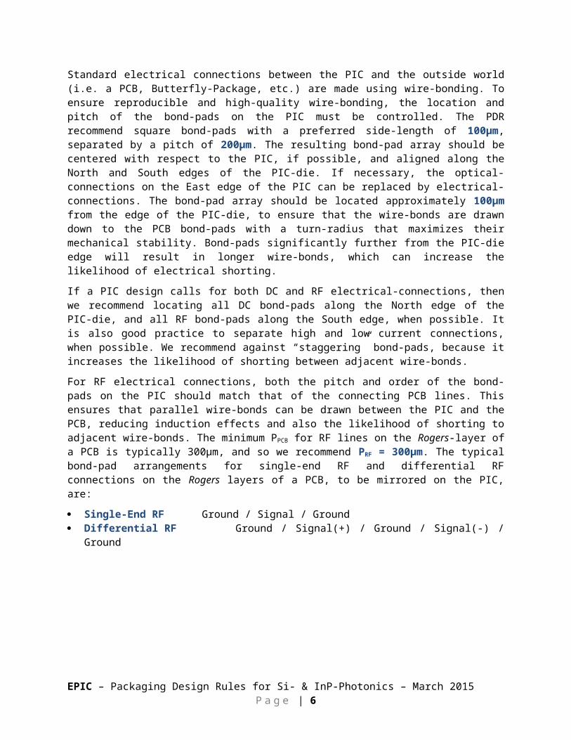
2.2 Electrical-Connections to the PICStandard electrical connections between the PIC and the outside world (i.e. a PCB, Butterfly-Package, etc.) are made using wire-bonding. To ensure reproducible and high-quality wire-bonding, the location and pitch of the bond-pads on the PIC must be controlled. The PDR recommend square bond-pads with a preferred side-length of 100µm, separated by a pitch of 200µm. The resulting bond-pad array should be centered with respect to the PIC, if possible, and aligned along the North and South edges of the PIC-die. If necessary, the optical-connections on the East edge of the PIC can be replaced by electrical-connections. The bond-pad array should be located approximately 100µm from the edge of the PIC-die, to ensure that the wire-bonds are drawn down to the PCB bond-pads with a turn-radius that maximizes their mechanical stability. Bond-pads significantly further from the PIC-die edge will result in longer wire-bonds, which can increase the likelihood of electrical shorting.
If a PIC design calls for both DC and RF electrical-connections, then we recommend locating all DC bond-pads along the North edge of the PIC-die, and all RF bond-pads along the South edge, when possible. It is also good practice to separate high and low current connections, when possible. We recommend against “staggering” bond-pads, because it increases the likelihood of shorting between adjacent wire-bonds.
For RF electrical connections, both the pitch and order of the bond-pads on the PIC should match that of the connecting PCB lines. This ensures that parallel wire-bonds can be drawn between the PIC and the PCB, reducing induction effects and also the likelihood of shorting to adjacent wire-bonds. The minimum PPCB for RF lines on the Rogers-layer of a PCB is typically 300µm, and so we recommend PRF = 300µm. The typical bond-pad arrangements for single-end RF and differential RF connections on the Rogers layers of a PCB, to be mirrored on the PIC, are:
Single-End RF Ground / Signal / Ground Differential RF Ground / Signal(+) / Ground / Signal(-) / Ground
EPIC – Packaging Design Rules for Si- & InP-Photonics – March 2015 P a g e | 3

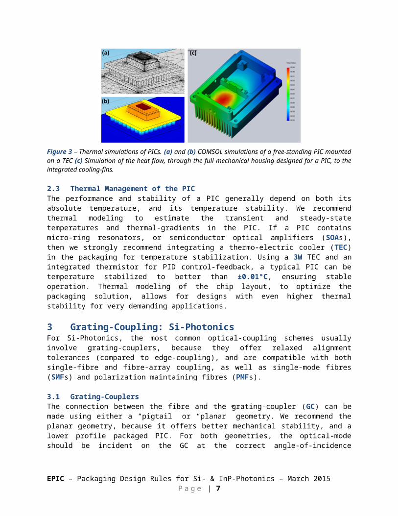
Figure 3 – Thermal simulations of PICs. (a) and (b) COMSOL simulations of a free-standing PIC mounted on a TEC (c) Simulation of the heat flow, through the full mechanical housing designed for a PIC, to the integrated cooling-fins.
2.3 Thermal Management of the PICThe performance and stability of a PIC generally depend on both its absolute temperature, and its temperature stability. We recommend thermal modeling to estimate the transient and steady-state temperatures and thermal-gradients in the PIC. If a PIC contains micro-ring resonators, or semiconductor optical amplifiers (SOAs), then we strongly recommend integrating a thermo-electric cooler (TEC) in the packaging for temperature stabilization. Using a 3W TEC and an integrated thermistor for PID control-feedback, a typical PIC can be temperature stabilized to better than ±0.01°C, ensuring stable operation. Thermal modeling of the chip layout, to optimize the packaging solution, allows for designs with even higher thermal stability for very demanding applications.
3 Grating-Coupling: Si-PhotonicsFor Si-Photonics, the most common optical-coupling schemes usually involve grating-couplers, because they offer relaxed alignment tolerances (compared to edge-coupling), and are compatible with both single-fibre and fibre-array coupling, as well as single-mode fibres (SMFs) and polarization maintaining fibres (PMFs).
3.1 Grating-CouplersThe connection between the fibre and the grating-coupler (GC) can be made using either a “pigtail” or “planar” geometry. We recommend the planar geometry, because it offers better mechanical stability, and a lower profile packaged PIC. For both geometries, the optical-mode should be incident on the GC at the correct angle-of-incidence (typically 8deg or 10deg), to ensure maximum coupling-efficiency at the target-wavelength.
Figure 4 – Optical connections to Si-PICs using grating-couplers. (a) The GC-arrays should be centred with respect to the PIC. (b) Schematic of the pigtail coupling-geometry between fibre and PIC, with a single fibre. (c) Schematic of the planar coupling-geometry, with a single fibre.
EPIC – Packaging Design Rules for Si- & InP-Photonics – March 2015 P a g e | 4

Figure 5 – Grating coupling for Si-Photonics. (a) Side-view of a pigtail fibre-array coupled to a PIC, showing the effect of over-shadowing from the glass end-cap, creating a significant “exclusion zone” on the PIC surface. (b) Side-view of a planar fibre-array coupled to a PIC, showing the “exclusion zone” needed to account for epoxy flow during bonding. (c) Schematic of a grating-coupler array with optical shunt. The pitch of the grating-coupler array matches the separation of individual fibres in the array (usually 127µm or 250µm). The top-view of the “exclusion zones” from the pigtail and planar coupling geometries are also shown, highlighted in red and orange.
The typical in-plane alignment tolerance for a GC is -1dB for ±2µm, so active optical-feedback is needed to optimally align the fibre with respect to the GC. For a “straight through” fibre-PIC-fibre coupling-scheme, the fibre-to-GC alignment can be optimized by simply maximizing the overall fibre-to-fibre transmission. Alternatively, the signal from an “onboard” Ge-photodiode, integrated into the Si-PIC, can be used to provide feedback for the alignment.
3.2 Coupling to Fibre-ArraysIf neither of these options is available, then a fibre-array with an optical-shunt can be used to make the fibre-to-GC alignment. This scheme has the advantage that it can be used to simultaneously make multiple fibre-to-GC alignments. To allow for multi-channel coupling between a fibre-array and an array of grating-couplers on the PIC, the following design rules should be followed:
The grating-coupler array should be arranged in a straight line, parallel to the edge of the PIC-die The pitch of the grating-coupler array (PG) should match the fibre diameters The grating-coupler array should be 0.5-1.0mm from the edge of the PIC-die The grating-coupler array should be centered with respect to the PIC The first and last channels of the grating-coupler array should be connected to form the shunt
When choosing the number of channels needed for their PIC, users should account for the two channels needed for the optical-shunt. Active alignment of the fibre-array, maximizing fibre-to-fibre transmission through the optical-shunt, ensures that all the intermediate channels in the fibre-array are well aligned with respect to the intermediate channels in the grating-coupler array. This approach works well with both SMF and PMF fibre-arrays, provided the pitch of the grating-coupler array exactly matches the diameters of the fibres being used, i.e. PG = 250µm or 127µm.
EPIC – Packaging Design Rules for Si- & InP-Photonics – March 2015 P a g e | 5
The fibre(-array) is typically bonded to the PIC using UV-cured epoxy. To ensure a stable mechanical- and optical-connection of the epoxy-bond, it is important to have sufficient contact area between the fibre and PIC. We recommend locating grating-couplers and grating-coupler arrays 0.5mm – 1.0mm from the edge of the PIC-die, in order to leave enough room for a strong bond. In addition, we recommend allowing for epoxy flow from the target region onto the main body of the PIC. For single-fibres and fibre-arrays in the planar coupling geometry, we suggest leaving an “exclusion zone” of up to 0.5mm, between the grating-couplers and the centre of the PIC, in which no bond-pads are located, because it is liable to be covered by the epoxy flow. For fibre-arrays in the pigtail geometry, “over-shadowing” from the glass end-cap of the array typically extends the bond-pad “exclusion zone” to 1.4mm towards the center of the PIC-die.
3.3 Extension to InP-PhotonicsGrating-couplers are most often used in the Silicon material platform, but can be transferred to InP-photonics applications without losing any key performance specifications. Although the coupler design will need to be modified at the microscopic level, to account for the different refractive indices and layer thicknesses of the materials being used, the macroscopic PDRs will remain the same.
Figure 6 – Images of an edge-coupled InP-PIC in a “Butterfly” package. (a) CAD design of the packaged PIC used to check the design of the proposed ceramic interposer, integrated TEC and other components of the final package. (b) Microscope image of a lensed-fibre in a metal ferrule, laser-welded into position, after active alignment to maximize the edge-coupling efficiency to a laser-chip
4 Edge-Coupling: InP and TriPleX-PhotonicsFor edge-coupling, the insertion loss is determined by the mode mismatch (i.e. the spot-size) between the fibre and chip, and their alignment accuracy. The better the match is between the spot-size of the optical output and the coupling-counterpart, i.e. the fibre(-array) or other optical chip, the higher the maximum coupling-efficiency . The smaller the spot-sizes involved, the tighter the alignment tolerances needed to reach the maximum coupling-efficiency. Currently, different foundries supply chips with markedly different the spot-sizes, due to the different chip thickness and technologies being used. In particular, InP-chips are very thin. The hope is for a standardization towards a spot-size matching that used in fibre-arrays (i.e. 10µm), though this is not yet technologically feasible.
4.1 Single fibre Coupling For edge-coupling, active alignment of the fibre(-array) is the only practical route. We advise users to include an integrated photodiode in their design, or to include an optical-shunt between for fibre-array coupling (in analogy to that described in Section 3.2). The alignment tolerances for edge-coupling are significantly more stringent than for grating-coupling, and this tends to reduce the flexibility of edge-
EPIC – Packaging Design Rules for Si- & InP-Photonics – March 2015 P a g e | 6
coupling packaging solutions. However, edge-coupling with a lensed (to a 3µm, or smaller, spot) or cleaved fibre (to a 10µm spot) allows for practical fibre-to-chip coupling. If the fibre is mounted in a metallic ferrule, then it can be conveniently “locked” into the optimum alignment position by laser-welding (i.e. to a Kovar Butterfly-package) using industry-standard equipment.
4.2 Coupling to Fibre-ArraysWhen edge-coupling to a fibre-array is needed for the packaging of the PIC, then we recommend following these PDRs:
The individual fibres should have their cores aligned in the same direction The pitch of the array should be set to 127µm or 250µm A lensed fibre-array should be used, if available
Without a lensed fibre-array, the coupling-efficiency to waveguides with spot-sizes <10µm is significantly reduced. To limit back-reflections from the coupling surfaces, the waveguides can be fabricated with slightly off-normal end-facets (typically 8deg for flat-fibres to InP). For coupling between a fibre-array and these angled waveguides, a geometric correction is need to ensure that the pitch of the wave-guides matches the separation of the fibres in the the fibre-array.
An alternative approach to using a lensed fibre-array is to use an TriPLeX interposer-chip. Here, the advantage is that the pitch and spot-size between the fibre-array and the waveguide-array can be matched, allowing for enhanced alignment-accuracy and coupling-efficiency. Moreover, photonic functionality can be engineered into the TriPLex interposer chip, allowing for richer PIC designs. The principle drawbacks of using an interposer are the increased material costs, and the increase in packaging complexity arising from adding an extra off-chip component.
4.3 Extension to Si-PhotonicsEdge-coupling is most often used in the InP material platform, because it is well suited to laser-to-fibre coupling. However, edge-coupling can be transferred to Si-photonics, following two schemes:
Optical-coupling between a lensed fibre and an inverted-taper on the Si-PIC Optical-coupling between a standard fibre and a 10µm mode-converter on the Si-PIC
In both cases, the user must ensure that their inverted-taper or mode-converter structure is sufficiently close to the edge of the PIC-die for fibre-access. Precision polishing of the PIC-die is typically needed, as well as post-processing with polymer layers, when a mode-converter is used.
5 Conclusion & ContactsThe goal of these PDRs is to help users design PICs that are compatible with practical photonic-packaging solutions. PICs based on the PDRs and best-practice suggestions in this document will benefit from improved coupling performance and reproducibility, as well as reduced packaging costs and assembly times.
For further details on photonics-packaging solutions, please contact:
Carlos Lee, Director GeneralEPIC – European Photonics Industry Consortium14 Rue de la Science, 1040 Brussels, BelgiumMobile: +32 473 300433 / Skype: carlos.lee.epic / Twitter: [email protected]
EPIC – Packaging Design Rules for Si- & InP-Photonics – March 2015 P a g e | 7


