Page 1
1
© 2011 Xilinx, Inc. All Rights Reserved
Basic Xilinx Design Capture
This material exempt per Department of Commerce license exception TSU
© 2011 Xilinx, Inc. All Rights Reserved For Academic Use Only
Basic XDC 2
Objectives
After completing this module, you will be able to:
• List various blocksets available in System Generator
• Describe how signals are fed to and results are read from a System
Generator based design
• List various data types supported by System Generator
• Identify steps involved in performing hardware-in-the-loop
verification
• State how hardware-in-the-loop verification is beneficial for complex
system designs
Page 2
2
© 2011 Xilinx, Inc. All Rights Reserved For Academic Use Only
Basic XDC 3
Outline
• Gateway In/Gateway Out
• Data Types
• Constructing Design Using
Xilinx Design Capture
• System Generator Block
• HDL Co-Simulation
• Hardware Verification
• Summary
© 2011 Xilinx, Inc. All Rights Reserved For Academic Use Only
Basic XDC 4
Interacting with SysGen Design
• The Simulink environment uses a “double” to represent numbers in a simulation.
A double is a 64-bit twos complement floating point number
– Because the binary point can move, a double can represent any number
between +/- 9.223 x 10¹⁸ with a resolution of 1.08 x 10⁻¹⁹…a wide desirable
range, but not efficient or realistic for FPGAs
• The Xilinx blockset uses n-bit fixed point numbers (twos complement optional)
• Thus, a conversion is required when Xilinx blocks communicate with Simulink
blocks (Xilinx Blockset →MATLAB I/O → Gateway In/Out)
Page 3
3
© 2011 Xilinx, Inc. All Rights Reserved For Academic Use Only
Basic XDC 5
Gateway In
• The Gateway In block support parameters to control the conversion from double-
precision to N-bit Boolean, signed (2’s complement), or unsigned fixed-point
precision
• During conversion the block provides options to handle extra bits
• Defines top-level input ports in the HDL design generated by System Generator
• Defines testbench stimuli when the Create Testbench box is checked in the
System Generator block
• Names the corresponding port in the top level HDL entity
© 2011 Xilinx, Inc. All Rights Reserved For Academic Use Only
Basic XDC 6
Gateway Out
• The Gateway Out block converts data from System Generator fixed point type
to Simulink double
• Defines I/O ports for the top level of the HDL design generated by System
Generator
• Names the corresponding output port on the top level HDL entity provided the
option is selected
Page 4
4
© 2011 Xilinx, Inc. All Rights Reserved For Academic Use Only
Basic XDC 7
Outline
• Gateway In/Gateway Out
• Data Types
• Constructing Design Using
Xilinx Design Capture
• System Generator Block
• HDL Co-Simulation
• Hardware Verification
• Summary
© 2011 Xilinx, Inc. All Rights Reserved For Academic Use Only
Basic XDC 8
FIX and UFIX Types
• FIX data type produces a signed twos
complement number
• UFIX data type produces unsigned
number
• When the output of a block is user
defined, the number is further
conditioned according to the selected
Quantization and Overflow options
FIX UFIX
Page 5
5
© 2011 Xilinx, Inc. All Rights Reserved For Academic Use Only
Basic XDC 9
Boolean and DSP48 Types
• The Xilinx blockset also uses the type
Boolean for control ports, such as CE
and RESET
• The Boolean type is a variant of the one-
bit unsigned number in that it will always
be defined (High or Low).
• A one-bit unsigned number can become
invalid; a Boolean
type cannot
• The DSP48 type is accessible
when you parameterize a constant—it is
helpful when driving the OPMODE input of
the DSP48 block
© 2011 Xilinx, Inc. All Rights Reserved For Academic Use Only
Basic XDC 10
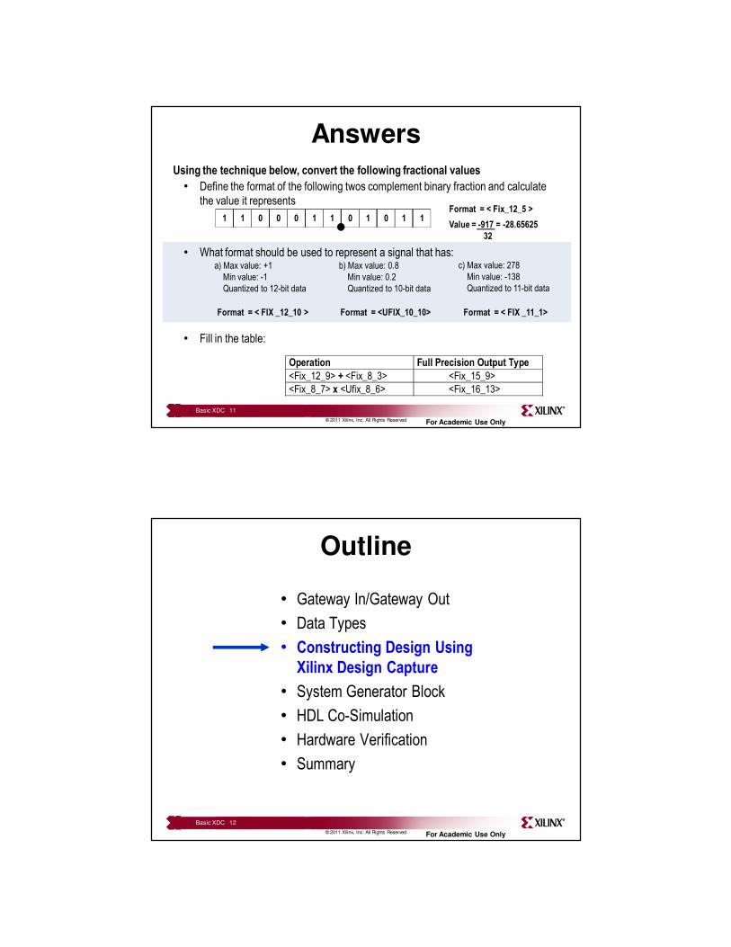
Knowledge Check
• Define the format of the following twos complement binary fraction and calculate
the value it represents
• What format should be used to represent a signal that has:
• Fill in the table:
Using the technique below, convert the following fractional values
1 1 0 0 0 1 1 0 1 0 1 1Format = < _ _ >
Value =
Format = < _ _ > Format = < _ _ > Format = < _ _ >
Operation Full Precision Output Type
<Fix_12_9> + <Fix_8_3>
<Fix_8_7> x <Ufix_8_6>
a) Max value: +1
Min value: -1
Quantized to 12-bit data
b) Max value: 0.8
Min value: 0.2
Quantized to 10-bit data
c) Max value: 278
Min value: -138
Quantized to 11-bit data
Page 6
6
© 2011 Xilinx, Inc. All Rights Reserved For Academic Use Only
Basic XDC 11
• Define the format of the following twos complement binary fraction and calculate
the value it represents
• What format should be used to represent a signal that has:
• Fill in the table:
Using the technique below, convert the following fractional values
1 1 0 0 0 1 1 0 1 0 1 1Format = < Fix_12_5 >
Value = -917 = -28.65625
32
Format = < FIX _12_10 > Format = <UFIX_10_10> Format = < FIX _11_1>
Operation Full Precision Output Type
<Fix_12_9> + <Fix_8_3> <Fix_15_9>
<Fix_8_7> x <Ufix_8_6> <Fix_16_13>
a) Max value: +1
Min value: -1
Quantized to 12-bit data
b) Max value: 0.8
Min value: 0.2
Quantized to 10-bit data
c) Max value: 278
Min value: -138
Quantized to 11-bit data
Answers
© 2011 Xilinx, Inc. All Rights Reserved For Academic Use Only
Basic XDC 12
Outline
• Gateway In/Gateway Out
• Data Types
• Constructing Design Using
Xilinx Design Capture
• System Generator Block
• HDL Co-Simulation
• Hardware Verification
• Summary
Page 7
7
© 2011 Xilinx, Inc. All Rights Reserved For Academic Use Only
Basic XDC 13
Creating a System Generator Design
Open the Simulink library browser by clicking the Simulink library browser button
Click on New Model button to create a blank model page
Use the Xilinx DSP blockset to capture the design
© 2011 Xilinx, Inc. All Rights Reserved For Academic Use Only
Basic XDC 14
Creating a SystemGenerator Design
• Build the design by dragging and dropping blocks from the Xilinx blockset onto your new sheet
• Design entry is similar to a schematic editor
Connect blocks by pulling
the arrows at the sides of
each block
Page 8
8
© 2011 Xilinx, Inc. All Rights Reserved For Academic Use Only
Basic XDC 15
Finding Blocks• Use the Find feature to search ALL
Simulink libraries
• The Xilinx blockset has eleven major
sections
– AXI4: FFT, VDMA
– Basic elements: counters, delays
– Communication: error correction blocks
– Control Logic: MCode, black box
– DSP: FDATool, FFT, FIR
– Data Types: convert, slice
– Index: all Xilinx blocks (a quick way to
view all blocks)
– Math: multiply, accumulate, inverter
– Memory: dual port RAM, single port RAM
– Shared memory: FIFO
– Tools: ModelSim, resource estimator
© 2011 Xilinx, Inc. All Rights Reserved For Academic Use Only
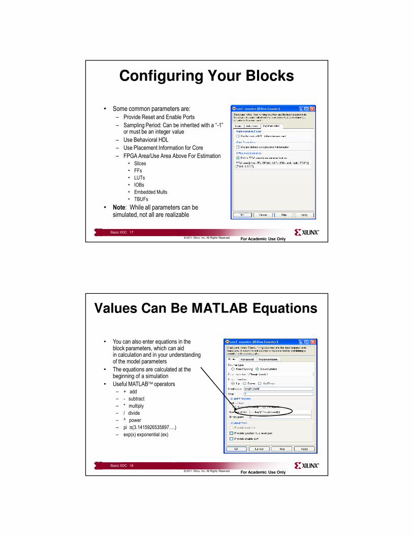
Basic XDC 16
Configuring Your Blocks
• Double-click or go to Block Parameters
to view and change the configurable parameters
of a block using multi-tabbed GUI
• Number of tabs and type of configurable
parameters under each tab is block dependent
• Some common parameters are:
– Precision: User defined or full precision
– Arithmetic Type: Unsigned or twos complement
– Number of Bits: total and fraction
– Overflow and quantization: Saturate or wrap
overflow, truncate or round quantization
– Latency: Specify the delay through the block
• Note: While all parameters can be simulated,
not all are realizable
Page 9
9
© 2011 Xilinx, Inc. All Rights Reserved For Academic Use Only
Basic XDC 17
Configuring Your Blocks
• Some common parameters are:
– Provide Reset and Enable Ports
– Sampling Period: Can be inherited with a “-1” or must be an integer value
– Use Behavioral HDL
– Use Placement Information for Core
– FPGA Area/Use Area Above For Estimation
• Slices
• FFs
• LUTs
• IOBs
• Embedded Mults
• TBUFs
• Note: While all parameters can be simulated, not all are realizable
© 2011 Xilinx, Inc. All Rights Reserved For Academic Use Only
Basic XDC 18
Values Can Be MATLAB Equations
• You can also enter equations in the block parameters, which can aid in calculation and in your understanding of the model parameters
• The equations are calculated at the beginning of a simulation
• Useful MATLAB operators
– + add
– - subtract
– * multiply
– / divide
– ^ power
– pi π(3.1415926535897.…)
– exp(x) exponential (ex)
Page 10
10
© 2011 Xilinx, Inc. All Rights Reserved For Academic Use Only
Basic XDC 19
Creating a SystemGenerator Design
Simulink
Sources
Simulink
Sinks
Gateway blocks used to interface
between Simulink and SysGen blocks
SysGen Data Path and
helper blocks
© 2011 Xilinx, Inc. All Rights Reserved For Academic Use Only
Basic XDC 20
System Generator Design
• All SysGen design must contain a System Generator block
• Used to set global netlisting attributes
• Designs may have levels of hierarchy
• Double click to “push” into a subsystem
Start simulation by pressing the play button
Page 11
11
© 2011 Xilinx, Inc. All Rights Reserved For Academic Use Only
Basic XDC 21
Outline
• Gateway In/Gateway Out
• Data Types
• Constructing Design Using
Xilinx Design Capture
• System Generator Block
• HDL Co-Simulation
• Hardware Verification
• Summary
© 2011 Xilinx, Inc. All Rights Reserved For Academic Use Only
Basic XDC 22
Sample Period
• Every System Generator signal must be “sampled”; transitions occur at equidistant discrete points in time, called sample times
• Each block in a Simulink design has a “sample period,” and it corresponds to how often the function of that block is calculated and the results outputted
• The sample period of a block directly relates to how that block will be clocked in the actual hardware
• This sample period must be set explicitly for:
• Gateway In
• Blocks without inputs (Note: constants are idiosyncratic)
• The sample period can be “derived” from the input sample times for other blocks
• Remember Nyquist’s theorem (Fs ≥ 2fmax) when setting sample periods
Page 12
12
© 2011 Xilinx, Inc. All Rights Reserved For Academic Use Only
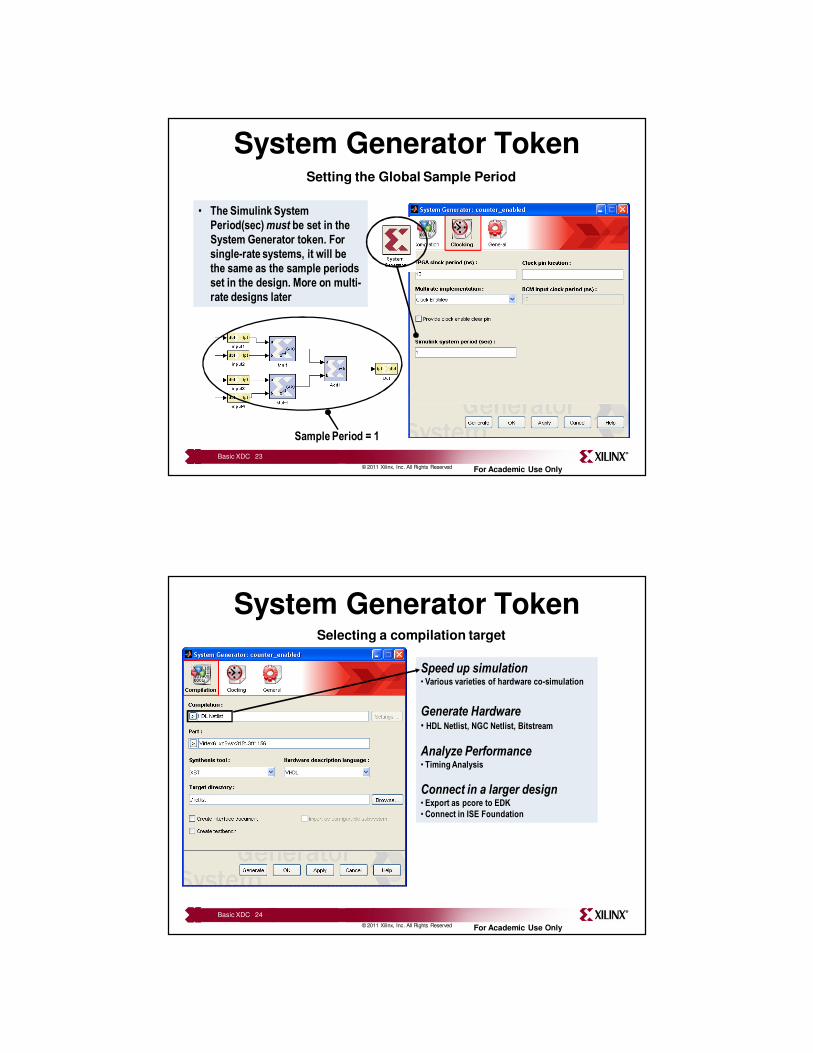
Basic XDC 23
System Generator TokenSetting the Global Sample Period
• The Simulink System
Period(sec) must be set in the
System Generator token. For
single-rate systems, it will be
the same as the sample periods
set in the design. More on multi-
rate designs later
Sample Period = 1
© 2011 Xilinx, Inc. All Rights Reserved For Academic Use Only
Basic XDC 24
System Generator Token
Speed up simulation• Various varieties of hardware co-simulation
Generate Hardware• HDL Netlist, NGC Netlist, Bitstream
Analyze Performance• Timing Analysis
Connect in a larger design• Export as pcore to EDK
• Connect in ISE Foundation
Selecting a compilation target
Page 13
13
© 2011 Xilinx, Inc. All Rights Reserved For Academic Use Only
Basic XDC 25
System Generator Token
• Specify the implementation Parameters
– HDL Netlist as the compilation mode
– Select the target part
– Set HDL language
– Set the FPGA Clock Period (in
Clocking tab)
– Check Create Testbench
• Generate the HDL
Once complete, double-click
the System Generator token
Generating HDL Code
© 2011 Xilinx, Inc. All Rights Reserved For Academic Use Only
Basic XDC 26
System Generator Output Files
• Design files
– VHD or V (HDL design files)
– EDN or NGC (core implementation file and netlist file)
– XCF (Xilinx constraints file for timing constraints)
• Project files
– ISE (Project Navigator project file)
– SGP (System Generator project file for Project Navigator)
– TCL (scripts for Synplify and Leonardo project creation)
• Simulation files
– DO (simulation scripts for MTI)
– DAT (data files containing the test vectors from System Generator)
– _tb.VHD or _tb.V (simulation testbench)
Page 14
14
© 2011 Xilinx, Inc. All Rights Reserved For Academic Use Only
Basic XDC 27
Outline
• Gateway In/Gateway Out
• Data Types
• Constructing Design Using
Xilinx Design Capture
• System Generator Block
• HDL Co-Simulation
• Hardware Verification
• Summary
© 2011 Xilinx, Inc. All Rights Reserved For Academic Use Only
Black Box
• Allows a way to import HDL models into
System Generator
• Allows co-simulation of black box HDL
with Simulink by using either the
ModelSim or the ISE® Simulator tool
• Integrates the imported HDL and
implementation files (EDN, NGC) with
the netlist generated from System
Generator
Basic XDC 28
Page 15
15
© 2011 Xilinx, Inc. All Rights Reserved For Academic Use Only
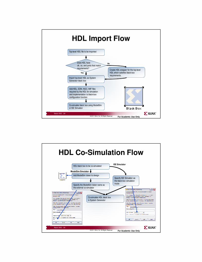
HDL Import Flow
Yes
No
Top-level HDL file to be imported
Import top-level HDL as System
Generator black box
Add HDL, EDN, NGC, MIF files
required by the HDL for simulation
and implementation to black-box
configuration function
Co-simulate black box using ModelSim
or ISE Simulator
Create HDL wrapper for the top-level
HDL which satisfies black-box
requirements.
Does HDL have
clk, ce, and ports that match
requirements?
Basic XDC 29
© 2011 Xilinx, Inc. All Rights Reserved For Academic Use Only
HDL Co-Simulation Flow
ISE Simulator
ModelSim Simulator
Co-simulate HDL black box
in System Generator
Specify the ModelSim token name as
the external co-simulator
Add ModelSim token to design
HDL black box to be co-simulated
Specify ISE Simulator as
the black-box simulation
mode
Basic XDC 30
Page 16
16
© 2011 Xilinx, Inc. All Rights Reserved For Academic Use Only
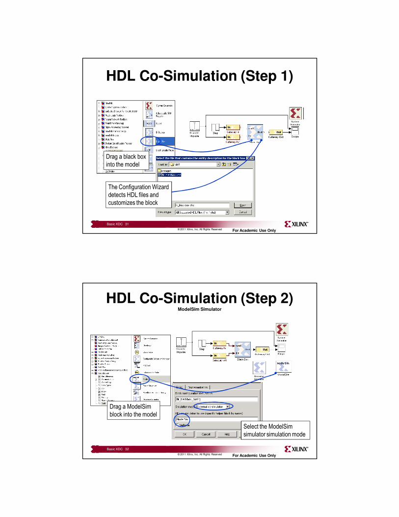
HDL Co-Simulation (Step 1)
Drag a black box
into the model
The Configuration Wizard
detects HDL files and
customizes the block
Basic XDC 31
© 2011 Xilinx, Inc. All Rights Reserved For Academic Use Only
HDL Co-Simulation (Step 2)ModelSim Simulator
Drag a ModelSim
block into the model
Select the ModelSim
simulator simulation mode
Basic XDC 32
Page 17
17
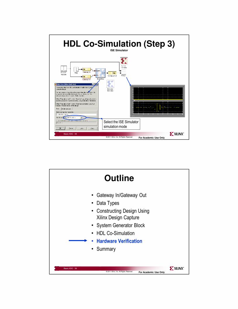
© 2011 Xilinx, Inc. All Rights Reserved For Academic Use Only
HDL Co-Simulation (Step 2)ISE Simulator
Select the ISE Simulator
simulation mode
Basic XDC 33
© 2011 Xilinx, Inc. All Rights Reserved For Academic Use Only
HDL Co-Simulation (Step 3)ModelSim Simulator
Select the External
co-simulator
simulation mode Simulink software opens
ModelSim simulator and
co-simulates
Basic XDC 34
Page 18
18
© 2011 Xilinx, Inc. All Rights Reserved For Academic Use Only
HDL Co-Simulation (Step 3)ISE Simulator
Select the ISE Simulator
simulation mode
Basic XDC 35
© 2011 Xilinx, Inc. All Rights Reserved For Academic Use Only
Basic XDC 36
Outline
• Gateway In/Gateway Out
• Data Types
• Constructing Design Using
Xilinx Design Capture
• System Generator Block
• HDL Co-Simulation
• Hardware Verification
• Summary
Page 19
19
© 2011 Xilinx, Inc. All Rights Reserved For Academic Use Only
Basic XDC 37
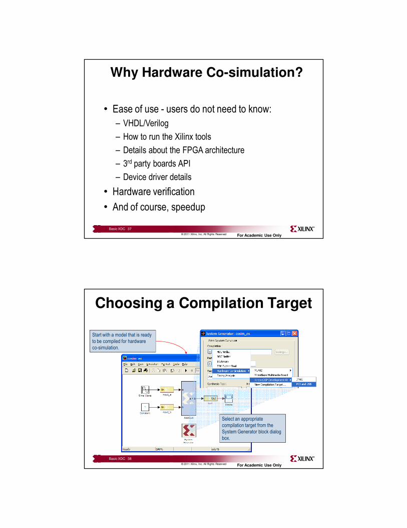
Why Hardware Co-simulation?
• Ease of use - users do not need to know:
– VHDL/Verilog
– How to run the Xilinx tools
– Details about the FPGA architecture
– 3rd party boards API
– Device driver details
• Hardware verification
• And of course, speedup
© 2011 Xilinx, Inc. All Rights Reserved For Academic Use Only
Basic XDC 38
Choosing a Compilation Target
Select an appropriate
compilation target from the
System Generator block dialog
box.
Start with a model that is ready
to be compiled for hardware
co-simulation.
Page 20
20
© 2011 Xilinx, Inc. All Rights Reserved For Academic Use Only
Basic XDC 39
Design Compilation
User presses
the Generate
button.
Design is automatically
compiled to produce a
bitstream.
© 2011 Xilinx, Inc. All Rights Reserved For Academic Use Only
Basic XDC 40
Run-time Co-simulation Blocks
The co-simulation run-time
block is added to the original
user model.
The post-generation function
creates a new library
containing a parameterized
run-time co-simulation block.
Page 21
21
© 2011 Xilinx, Inc. All Rights Reserved For Academic Use Only
Basic XDC 41
Choosing an Interface
• PCI/PCMCIA
– Specialized co-simulation interfaces for a handful of boards (i.e., not a general
solution)
– Fastest co-simulation solution.
– Ideally suited for high-bandwidth co-simulation applications
• JTAG (Parallel/USB)
– Support for any board with a Xilinx FPGA, JTAG header, and clock source
– Burst-transfer support
• 1 Mbps down to the board
• 0.5 Mbps back from the board
• Ethernet
– Point-to-point
– Network-based
© 2011 Xilinx, Inc. All Rights Reserved For Academic Use Only
Basic XDC 42
Ethernet Hardware Co-simulation
• Two flavors:
– Network-based
• Remote access
• 10/100/1000 Base-T
• Ethernet-based configuration
– Point-to-Point
• Requires a direct connection between host PC and FPGA
• 10/100/1000 Base-T
• Ethernet configuration
Page 22
22
© 2011 Xilinx, Inc. All Rights Reserved For Academic Use Only
Basic XDC 43
Outline
• Gateway In/Gateway Out
• Data Types
• Constructing Design Using
Xilinx Design Capture
• System Generator Block
• HDL Co-Simulation
• Hardware Verification
• Summary
© 2011 Xilinx, Inc. All Rights Reserved For Academic Use Only
Basic XDC 44
Knowledge CheckKnowledge Check
Page 23
23
© 2011 Xilinx, Inc. All Rights Reserved For Academic Use Only
Basic XDC 45
Knowledge Check
• Describe the steps involved in hardware-in-the-
loop verification
© 2011 Xilinx, Inc. All Rights Reserved For Academic Use Only
Basic XDC 46
Answers
• Describe the steps involved in hardware-in-the-
loop verification– Hardware-in-the-loop is a Simulink hardware accelerator which
enables design verification in hardware. It is a Simulink-to-
bitstream-to-Simulink push-button flow to simulate HDL-based
and EDIF-based design
– Three simple steps
• Select the target board as a compilation option in the System
Generator token
• Compile (Generate) the design for the co-simulation
• Copy a co-simulation run-time block into the user model
Page 24
24
© 2011 Xilinx, Inc. All Rights Reserved For Academic Use Only
Basic XDC 47
Knowledge Check
• List data types supported by the Xilinx System
Generator blocks
© 2011 Xilinx, Inc. All Rights Reserved For Academic Use Only
Basic XDC 48
Answers
• List data types supported by the Xilinx System
Generator blocks– Twos complement signed (FIX)
– Unsigned (UFIX)
– Boolean
– DSP48
Page 25
25
© 2011 Xilinx, Inc. All Rights Reserved For Academic Use Only
Basic XDC 49
Summary
• Every System Generator design interfaces with Simulink
sources/sinks/blocks using Gateway In and Gateway Out
blocks
• Gateway In block when realized in hardware provides
input port at a top hierarchy level
• Gateway Out block when realized in hardware provides
output port at a top level hierarchy level
• Hardware-in-the-loop enables verification of the design
using hardware
© 2011 Xilinx, Inc. All Rights Reserved For Academic Use Only
Basic XDC 50
Where Can I Learn More?
• Tool documentation
– Simulink Browser →→→→ Help →→→→ Simulink Help →→→→ Xilinx System Generator
• A Tutorial Introduction
• Using FPGA Hardware in the Loop
• Hardware Design Using System Generator →→→→ System Level Modeling
• Hardware Design Using System Generator →→→→ Automatic Code
Generation
• Examples
– <Matlab_install>\toolbox\xilinx\sysgen\examples
• Support Website
– DSP Website: http://www.xilinx.com/dsp


![XDC Dual Fiber CWDM series - XENYAsup.xenya.si/sup/info/xenya/wdm/[XWDM]_XDC_CWDM_DualFiberSeri… · XDC Dual Fiber CWDM series ... watermark peak attenuation, still allows transfer](https://static.documents.pub/doc/80x56/5adac9d37f8b9a53618d19fc/xdc-dual-fiber-cwdm-series-xwdmxdccwdmdualfiberserixdc-dual-fiber-cwdm.jpg)

