Toward transparent projection display: recent progress in frequency‐selective scattering of RGB light based on metallic nanoparticle’s localized surface plasmon resonance YiyangYe1,ZhenLiu2andTupeiChen1*
A transparent display simultaneously enables visualization of the images displayed on it as well as the view behind it,and therefore can be applied to, for instance, augmented reality (AR), virtual reality (VR), and head up display (HUD). Many solutions have been proposed for this purpose. Recently, the idea of frequency-selective scattering of red, green and blue light while transmitting visible light of other colours to achieve transparent projection display has been pro-posed, by taking advantage of metallic nanoparticle’s localized surface plasmon resonance (LSPR). In this article, a re-view of the recent progress of frequency-selective scattering of red, green and blue light that are based on metallic na-noparticle’s LSPR is presented. A discussion of method for choosing appropriate metal(s) is first given, followed by the definition of a figure of merit used to quantify the performance of a designed nanoparticle structure. Selective scatteringof various nanostructures, including sphere-shaped nanoparticles, ellipsoidal nanoparticles, super-sphere core-shell na-noparticles, metallic nanocubes, and metallic nanoparticles combined with gain materials, are discussed in detail. Each nanostructure has its own advantages and disadvantages, but the combination of the metallic nanoparticle with gain ma-terials is a more promising way since it has the potential to generate ultra-sharp scattering peaks (i.e., high frequen-cy-selectivity).
Introduction A transparent display simultaneously enables visualiza-tion of the images displayed on it as well as the view be-hind it. For this reason, transparent display can be applied in augmented reality in which an object appears to be floating in air, shop windows that show vivid images or video for advertisement purpose, and car head-up display where navigation or other information are displayed on a car’s windshield. Existing solutions for transparent display include those based on micro-lens array (MLA) systems1, projection-based fluorescent display2, and organic light emitting diode (OLED) based display3, each has its own advantages and subset of applications. Recently, the idea
of frequency-selective scattering of red, green and blue light and transmission of visible light of other colours to achieve transparent projection display has been proposed4–7, which takes advantage of metallic nanopar-ticle’s localized surface plasmon resonance (LSPR)8,9, and is schematically shown in Fig. 110. This article reviews recent progress of frequency-selective scattering of red, green and blue light that are based on metallic nanoparti-cle’s LSPR4–7.
A discussion of method for choosing appropriate met-al(s) is first given, followed by the definition of a figure of merit used to quantify the performance of a designed nanoparticle structure. We then review frequen-cy-selective scattering of sphere-shaped nanoparticles,
1School of Electrical and Electronic Engineering, Nanyang Technological University, Singapore 639798, Singapore. 2School of Materials and
Energy, Guangdong University of Technology, Guangzhou 510006, China.
ellipsoidal nanoparticles, super-sphere core-shell nano-particles, metallic nanocubes, and finally metallic nano-particles combined with gain materials.
Method for choosing metal Figure 1 shows the ideal case for the transparent projec-tion display based on metallic nanoparticle’s LSPR10. This method relies on the design of optical resonant scatterers that are strongly frequency-selective in light scattering and have low absorption in the wavelength range of visi-ble light. Metals are chosen by first checking whether they have the potential to generate sharp resonant peak(s) (i.e., strong frequency-selectivity). Two approaches have been proposed for this purpose4,7, and they lead to the same conclusion: around interested wavelengths (i.e., wave-lengths for red, green and blue light in this case), the die-lectric function of a qualified metal should have a small imaginary part or a real part with fast changing rate with respect to wavelength (or frequency).
Both approaches assume quasi-static approximation (i.e., particle size << wavelength) to give a rough estima-tion. For a metallic nanoparticle of arbitrary shapes, the first approach calculates the ratio of scattering cross sec-tion between the on-resonance (at resonant wavelength 0) and off-resonance (at 0 Δλ λ , with a small wavelength step Δλ ), which is given below4:
20 0sca 0
sca 0 0
Re ( Δ ) ( )1
( Δ ) Im ( )( ) λ λ λσ λ
σ λ λ λ
, (1)
where Re[·] and Im[·] denote real part and imaginary part of a complex number, respectively, and ( )λ de-notes the metal’s dielectric function at a wavelength λ . A sharp scattering peak is equivalent to a large value of the ratio shown in the left-hand-side of equation (1). There-
fore, by observing the right-hand-side of equation (1), it is obvious that a small imaginary part of the metal’s die-lectric function or a fast-changing real part of the metal’s dielectric function generates a sharp scattering peak, and hence a strong frequency selectivity. Derivation of equa-tion (1) is given in Ref.4.
The second approach looks at the resonance peak’s halfwidth *Γ (in eV)7:
* 02 2
2Im[ ](1 )
dRe[ ( )
(
] dIm[ ( )]d d
)ωΓ β
ω ωω ω
, (2)
where ω is incident light’s angular frequency (ω=2πc/, c is speed of light in vacuum), ω0 is the resonant frequency (i.e., ω0=2πc/0), and β is usually very small compared to 1 and can be neglected. The two derivatives in the de-nominator of equation (2) are taken at the resonant fre-quency ω0. Derivation of equation (2) is given in Ref.11. A strong frequency selectivity is equivalent to a narrow width of resonance peak. Thus, by observing equation (2), the second approach reaches the same conclusion as that from the first approach.
So, it is useful to plot 2
dRe / Imd
ηλ
in visible
spectrum range (400–800 nm), and choose a metal with a high η value. The η curves of different metals are shown in Fig. 24. It is obvious that silver (Ag) has the largest value for most part of the visible spectrum, while gold (Au) has the largest value around the wavelength of 700 nm. Therefore, Ag is the most suitable candidate for the whole visible spectrum, while Au may be suitable around red light.
Definition of figure of merit (FOM) For candidate metals, the next step is to check whether an optimal trade-off between light scattering frequen-cy-selectivity and light absorption can be achieved by tuning its structural parameters (for instance, core diam-eter, shell thickness for core-shell structure). For the
Fig. 1 | Schematic illustration of the concept of transparent
projection display achieved by frequency-selective scattering
of red, green and blue light. This demonstrates the ideal case:
light scattering spectrums have ultra-sharp peaks around the
central wavelengths of the three additive colours (red, green and
blue), while light absorption remains 0 all through the visible light
wavelength range. Figure reproduced with permission from Ref.10,
Optical Society of America.
Sca
tterin
g (
arb
.uni
ts)
1.0
0.8
0.6
0.4
0.2
0.0 400 450 500 550 600 650 700 750
Light of other wavelength transmitted
Laser light with RGB is scattered to form image
Wavelength (nm)
Fig. 2 | η as a function of wavelength in the visible light range
for various metals. Figure adapted by permission from Ref.4,
purpose of tuning structural parameters, it is necessary to quantize the desired performance by a mathematical ex-pression. To achieve this, the following figure of merit (FOM) is defined:
sca 0
sca abs
( )2 max{ }
σ λFOM
σ σ
, (3)
where scaσ and absσ are the scattering and absorption cross sections of a nanoparticle respectively which are affected by the nanoparticle’s shape, size, constituent ma-terial as well as surrounding medium8,9. They can be cal-culated by the Mie theory for spherical, ellipsoidal and cylindrical shapes12,13, or by numerical methods such as FDTD (finite-difference time domain) and DDA (discrete dipole approximation) for arbitrary shapes14,15. The overbar and the symbol absmax{ }σ respectively denote the mean and the maximum values in the visible spec-trum (from 400 nm to 800 nm). This FOM is first defined by Soljačić’s group4, and another two works followed this definition6,7. It is obvious from equation (3) that a high value of FOM favours the following properties: low ab-sorption cross-section over the whole visible spectrum, a high scattering cross-section at the resonance wavelength, and low scattering cross-section elsewhere, i.e. a narrow or sharp resonance peak. Therefore, the FOM suggests that to achieve a high performance, the scatterers should be strongly frequency-selective and have low absorption.
Nanoparticle structures for
frequency-selective scattering
Sphere-shaped nanoparticles Sphere-shaped nanoparticle is highly symmetric, and therefore does not need alignment when dispersed in a transparent matrix. Ag nanoparticle’s resonance peak wavelength under quasi-static approximation (i.e., parti-cle size<<wavelength) is about 416 nm when its sur-
rounding environment has a refractive index of 1.5, ac-cording to the resonance condition: m 0 sRe[ ( )] 2ε λ ε 8, where 0λ is the resonance peak wavelength and m 0( )ε λ is the metal’s dielectric function at this wavelength, and
ss2( )ε n is the surrounding medium’s dielectric function.
However, the wavelength ranges for blue, green and red light are 450–490 nm, 520–560 nm and 635–700 nm, respectively16. Thus, it is necessary to red-shift Ag nano-particle’s resonance peak wavelength under quasi-static limit into the three wavelength regions of red, green and blue light. For this purpose, two approaches have been proposed: the first one is the core-shell structure with silica as core and silver as shell (Silica/Ag)4, and the se-cond one is the core-shell structure with silver as core and TiO2 as shell (Ag/TiO2)7. In this section, selective scatter-ing of red, green and blue light based on Silica/Ag is first reviewed, followed by that based on Ag/TiO2. The works reported in Refs.4,7 are summarized below. Silica/Ag For the structure of Silica/Ag, optimization of FOM (as defined by equation (3)) is carried out using the mul-ti-level single-linkage algorithm17, which can be imple-mented within the free nonlinear optimization package NLopt18. It was assumed that the transparent matrix (Polyvinyl Alcohol, or PVA in short) in which nanoparti-cles of Silica/Ag are embedded has a refractive index of 1.444. Refractive index for silica is assumed to be 1.45 and dielectric constants for Ag is from Ref.19. However, it should be pointed out that direct usage of Ag’s dielectric constants from reference is not appropriate, as this omits effect of surface dispersion of conduction electrons which increases light absorption and deceases light scattering20,21, and this effect is numerically demonstrated later in the section: “Spheroidal nanoparticles”.
Optimized results from Silica/Ag are shown in Fig. 3 as well as Table 14.
Fig. 3 | Calculated scattering and absorption cross-sections for Silica/Ag nanoparticles (embedding medium has a refractive index of
1.44). And optimizations are performed for them to scatter monochromatic light at (a) 0=458 nm (blue), (b) 532 nm (green), and (c) 640 nm
(red). Relative sizes of the structures are shown by the insets; and r denotes the outer radius of the particle. Figure adapted by permission from
Table 1 | Optimal particle sizes and FOM for silica-core sil-
ver-shell nanoparticles.
Wavelength λ0 Core radius Shell thickness FOM
458 nm 1.3 nm 30.8 nm 1.01
532 nm 22.2 nm 15.8 nm 0.91
640 nm 34.3 nm 11.0 nm 0.81
Table adapted by permission from Ref.4, Springer Nature.
Due to difficulty in precise synthesis of Silica/Ag structure22, experimental verification was conducted only for blue-color-only transparent projection display with spherical Ag nanoparticles with average diameter of ~62 nm (silica core with radius of 1.3 nm is omitted)4. A blue-color-only transparent projection display was made by embedding spherical Ag nanoparticles with average diameter of 62 nm into PVA polymer-matrix4. This film has a thickness of 0.46 mm, and the areal concentration of Ag nanoparticles is about 6×10⁹/cm2, or an equivalent
mass concentration of 7 μg/cm2. As shown in Figs. 4(a) and 4(b)4, the measured transmittance and extinction spectrum agrees well with the results from simulations. The simulated results of light scattering and absorption in Fig. 4(b) indicates that on-resonance scattering is signifi-cantly stronger than the on-resonance absorption4, which may not remain true if effect of surface dispersion of conduction electrons is included. Angular distribution of scattered light shown in Fig. 4(c) indicates that the scat-tering is very isotropic and polarization-independent4. And these suggest the scattered light from the display can be viewed from a wide angle and the display can be oper-ated with incident light with arbitrary polarization.
In Fig. 54, the transparent projection display at work is shown. The projected image shows up clearly on the dis-play embedded with Ag nanoparticles. In comparison, the same image projected onto regular glass (photo on the right) can barely be seen due to the lack of scattering.
Fig. 4 | Characterization of the transparent projection film made by dispersing Ag nanospheres with average diameter of 62 nm in PVA.
(a) Comparison of the measured and theoretically calculated transmittance spectrums. The width of the experimentally measured curve stands
for one standard deviation over different wavelength of incident light. Inset is a TEM image of the Ag nanospheres with average diameter of 62±4
nm. Scale bar of the TEM image is 200 nm. (b) Comparison of extinction spectrums from experimental measurement and theoretical calculation,
and the theoretically calculated scattering and absorption are also shown. (c) Angular distribution of light scattering at the wavelength of 458 nm,
with electric field of the normally incident light polarized parallel (p) and perpendicular (s) to the scattering plane. Figure adapted by permission
from Ref.4, Springer Nature.
Fig. 5 | Comparison of the transparent projection display in work (left) with a normal piece of glass (right). A blue MIT icon is projected
onto both the transparent projection display and the normal glass by a laser projector (MicroVision SHOWWX+, wavelength of blue light is 458±
2 nm). The image can be viewed clearly on the transparent projection display, but not on the normal glass. Three cups with letters of red, green
and yellow colors are placed behind the screen to intuitively demonstrate the transparency. Figure adapted by permission from Ref.4, Springer
Ag/TiO2 Another way of red-shifting Ag’s resonance peak wave-length is by coating Ag nanosphere with a high-index dielectric shell8, such as TiO2, as reported in another work7.
For the structure of Ag/TiO2, optimization of its FOM is similar to that of Silica/Ag. It was assumed that the transparent matrix (PVA) in which nanoparticles of Ag/TiO2 are embedded has a refractive index of 1.57. Re-fractive index for TiO2 is assumed to be 1.8. The reason why a low refractive index for TiO2 is chosen rather than a value of 2.723 is that the chemical method employed produces amorphous TiO2 shell24, which usually has a much lower refractive index than that of rutile phase due to lower density25. The dielectric function of Ag has in-cluded the effect of surface scattering of conduction elec-trons since the silver core’s size is comparable to electron’s mean free path in bulk silver, which is about 52 nm21. The extra damping sγ caused by surface scattering of elec-trons is added to the bulk damping bγ to give the cor-rected dielectric function Cε for silver nanoparticles:
2 2p p
C expb b s( i ) [ i( )]
ω ωε ε
ω ω γ ω ω γ γ
, (4)
where expε is silver’s dielectric function from Ref.19 (ex-perimentally determined), ωp is the plasma frequency of silver, ω is the frequency of the incident light, and i is the imaginary number. In the optimization, ωp and γb are assumed to be 9.6 eV and 22.8 meV, respectively26. And γs is given by27:
Fs
Avγ
r , (5)
where νF=1.39×10⁶ m/s is the electron velocity at the Fermi surface for silver26, and r is the radius of the silver core, A is a dimensionless fitting number, whose value is not free from controversy: values from 0.1 to 2 have been theoretically justified28. Since A values of 0.25 and 0.8 have been experimentally reported27,28, an A value of 0.5 is chosen in the optimization.
As the blue-color-only transparent projection display has been demonstrated in Ref.4 and discussed above, the following discussion will only focus on selective scatter-ing of green light and red light based on Ag/TiO2. Opti-mized results of Ag/TiO2 are shown in Fig. 6 and Table 27.
Table 2 | Optimal particle sizes and FOM for silver-core
TiO2-shell nanoparticles.
Wavelength λ0 Core radius Shell thickness FOM
525 nm 35 nm 14 nm 0.8941
620 nm 37.5 nm 39 nm 0.8921
Table reproduced by permission from Ref.7, The Royal Society of
Chemistry.
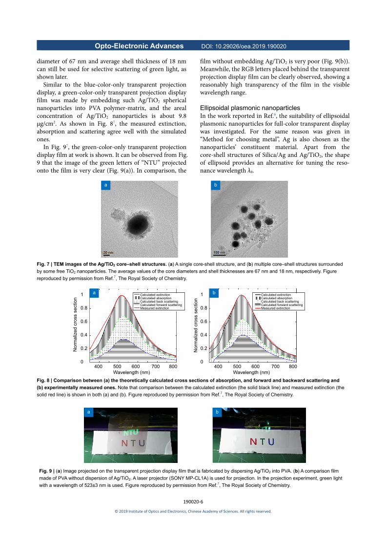
Due to the difficulty in coating thick TiO2 shell (i.e., it is difficult to control uniformity of the shell thickness), only the structure for selective scattering of green light was synthesized for experimental verification in the work reported in Ref.7. The nanoparticles used for experi-mental verification have average diameter of 67 nm and average shell thickness of 18 nm (Fig. 7)7, which are dif-ferent from the optimized values. This is due to the diffi-culty in precisely controlling the sizes of both the core (the core diameter shrinks during the synthesis process) and shell. Nevertheless, the nanoparticles with average
Fig. 6 | (a) Optimized results for green light selective scattering. (b) Optimized results for red light selective scattering. (c) Angular distribution of
scattered light for (a) at the wavelength of 525 nm. (d) Angular distribution of scattered light for (b) at the wavelength of 620 nm. Efficiency is the
corresponding cross section (i.e., extinction, scattering or absorption) divided by the nanoparticle’s geometrical cross section πr2, where r is
core-shell structure’s outer radius. The angular distributions of scattered light are calculated by assuming incident light has a unit intensity, and
equal components for the p- and s- polarization with respect to the scattering plane. Calculations are done with Mie’s theory. Figure reproduced
by permission from Ref.7, The Royal Society of Chemistry.
Scattering intensity versus scattering angle Scattering intensity versus scattering angle
diameter of 67 nm and average shell thickness of 18 nm can still be used for selective scattering of green light, as shown later.
Similar to the blue-color-only transparent projection display, a green-color-only transparent projection display film was made by embedding such Ag/TiO2 spherical nanoparticles into PVA polymer-matrix, and the areal concentration of Ag/TiO2 nanoparticles is about 9.8 μg/cm2. As shown in Fig. 87, the measured extinction, absorption and scattering agree well with the simulated ones.
In Fig. 97, the green-color-only transparent projection display film at work is shown. It can be observed from Fig. 9 that the image of the green letters of “NTU” projected onto the film is very clear (Fig. 9(a)). In comparison, the
film without embedding Ag/TiO2 is very poor (Fig. 9(b)). Meanwhile, the RGB letters placed behind the transparent projection display film can be clearly observed, showing a reasonably high transparency of the film in the visible wavelength range.
Ellipsoidal plasmonic nanoparticles In the work reported in Ref.6, the suitability of ellipsoidal plasmonic nanoparticles for full-color transparent display was investigated. For the same reason was given in “Method for choosing metal”, Ag is also chosen as the nanoparticles’ constituent material. Apart from the core-shell structures of Silica/Ag and Ag/TiO2, the shape of ellipsoid provides an alternative for tuning the reso-nance wavelength λ0.
Fig. 7 | TEM images of the Ag/TiO2 core–shell structures. (a) A single core-shell structure, and (b) multiple core–shell structures surrounded
by some free TiO2 nanoparticles. The average values of the core diameters and shell thicknesses are 67 nm and 18 nm, respectively. Figure
reproduced by permission from Ref.7, The Royal Society of Chemistry.
Fig. 8 | Comparison between (a) the theoretically calculated cross sections of absorption, and forward and backward scattering and
(b) experimentally measured ones. Note that comparison between the calculated extinction (the solid black line) and measured extinction (the
solid red line) is shown in both (a) and (b). Figure reproduced by permission from Ref.7, The Royal Society of Chemistry.
Fig. 9 | (a) Image projected on the transparent projection display film that is fabricated by dispersing Ag/TiO2 into PVA. (b) A comparison film
made of PVA without dispersion of Ag/TiO2. A laser projector (SONY MP-CL1A) is used for projection. In the projection experiment, green light
with a wavelength of 523±3 nm is used. Figure reproduced by permission from Ref.7, The Royal Society of Chemistry.
a b
a b
a Calculated extinctionCalculated absorption Calculated back scattering Calculated forward scatteringMeasured extinction
Wavelength (nm) 400 500 600 700 800
1 0.8 0.6 0.4 0.2 0
No
rmal
ized
cro
ss s
ect
ion
b Calculated extinction Calculated absorption Calculated back scattering Calculated forward scattering Measured extinction
The geometry array under consideration is shown in Fig. 106, which is composed of a bi-dimensional periodic array of Ag ellipsoids arranged in a square lattice and surrounded by a transparent dielectric matrix with die-lectric constant of εh. The distance between two adjacent Ag ellipsoids’ geometric centres is denoted with d, and is equal to 100 nm. The major semi-axis along the y-axis of the ellipsoids is denoted as a, and the two minor semi-axes b, c of the ellipsoids are assumed to be equal. The propagation direction of the incident light is as-sumed to be normal to the plane of the periodic array, and electric field oscillation of incident light is along the major semi-axis (i.e., a TE-plane wave).
Effect of surface scattering is taken into account in the same way as described in section “Ag/TiO2”, i.e., equations (4) and (5) are applicable to the ellipsoidal plasmonic
nanoparticles here; however, equation (5) is slightly mod-ified to account for difference between major and minor axes of ellipsoid, as given by the equation below:
Fsi
i
Avγ
r , (6)
where i(=a, b or c) represents the major semi-axis along y-axis or the two minor semi-axes of the ellipsoids, i.e., ra=a, rb=rc=b, and A is a correction factor. From equation (6), it is obvious that damping of free electrons along the major axis of ellipsoid is different from that along the minor axes. Therefore, the dielectric function of an ellip-soidal Ag nanoparticle is slightly anisotropic.
Through an analytical model29–33, it is concluded that resonance peak wavelength of a Ag ellipsoid is mainly affected by eccentricity, and that a trade-off between sharpness of scattering peak (i.e., frequency-selectivity of scattering) and light absorption level cannot be avoided when adjusting its size. And it is found that the eccen-tricity is equal to 0.96, 0.9, and 0.81 for the red, green, and blue arrays, respectively. Therefore, as a first estimation, it is useful to fix eccentricity of a set of Ag ellipsoids to 0.96, 0.9 or 0.81 and tune their major axis a to maximize FOM defined by equation (3). The result of this initial maximi-zation is shown as solid lines in Fig. 11(a)6.
For the nanoparticles array resonating in the red region, significantly higher FOM values can be observed in Fig. 11(a). This is mainly due to the fact that a non-neglectable portion of the scattering and absorption response of these arrays falls at the infrared wavelengths, and, thus, is excluded by the FOM computation.
In Fig. 11(a)6, FOM calculated without considering surface scattering of conduction electrons (i.e., directly use Ag’s dielectric constants from the literature)19 are also shown as dashed lines. It is clear that at smaller sizes, val-ues of FOM calculated without surface scattering are much larger than those calculated with surface scattering.
Fig. 11 | (a) Initial optimization of Ag ellipsoids for selective scattering of the three basic additive colours (red, green and blue) based on FOM.
For each basic array of Ag ellipsoids, the nanoparticles’ major axis is varied from 20 nm to 40 nm while their eccentricity is fixed at 0.96, 0.9,
and 0.81 for the red, green, and blue arrays, respectively. As a comparison, values of the FOM without consideration of effect of surface scat-
tering of conduction electrons are also shown (dashed lines). (b) Calculated cross sections for scattering (SCS) and absorption (ACS) for a Ag
ellipsoids array with the following parameters: a= 20 nm, b=c=12 nm, and d=100 nm. Both results with and without consideration of surface
scattering of free electrons (i.e., the size-correction) are shown. Figure reprinted with permission from Ref.6, AIP Publishing.
An intuitive understanding is gained from Fig. 11(b)6, where scattering and absorption spectrums are calculated for a nanoparticle array designed to resonate in the blue region (a=20 nm, b=c=12 nm, and d=100 nm) with and without surface scattering. From Fig. 11(b)6, it is clear that without consideration of surface scattering, scattering level is overestimated, and absorption level is underesti-mated.
Starting from the initially optimized results shown in Fig. 11(a)6, the final optimized Ag ellipsoids for red, green and blue light selective scattering are shown in Table 3.
Table 3 | Optimal particle sizes and FOM for ellipsoidal Ag
nanoparticles.
Wavelength λ0 a b FOM
461 nm 25 nm 17 nm 0.93
530 nm 26 nm 13 nm 1.1
678 nm 30 nm 9 nm 1.6
Table adapted with permission from Ref.6, AIP Publishing.
Since the optimized ellipsoidal Ag nanoparticles in Ta-ble 3 are obtained by assuming incident light to be TE-plane wave, the design shown in Fig. 12 is proposed
to realize a full-colour and almost polariza-tion-independent transparent projection display6.
The full-wave results of the proposed structure depict-ed by Fig. 12 are shown in Fig. 136, where results for both polarizations of incident light (i.e., oscillating electric field along the x- and y-axes) are plotted.
As observed from Fig. 136, the three scattering peaks are sharp, and the overall absorption level is reasonably low. Average transmittance calculated for the TE polariza-tion incidence is 52%. The small differences between re-sults of two incident polarizations are due to residual coupling among different layers. The 3D scattering pat-terns for the TE incident polarization of the optimized Ag ellipsoids in Table 3 are shown in Fig. 146, which indicates that the scattering patterns are almost isotropic.
The simulation in Ref.6 shows that when half of the el-lipsoids in the design in Fig. 12 are randomly shifted up to 15 nm in the xy-plane, the performance is not affected. Also, for the design in Fig. 12, it is shown that variation of eccentricity up to a minor axis change ratio of 2.5% does not have significant effect on performance. Thus, it is believed that the design in Fig. 12 has some robustness towards geometrical imperfections.
Fig. 12 | Proposed unit-cell of a full-color and almost polariza-
Super-sphere core-shell Apart from spherical core-shell nanoparticles, the struc-ture of super-sphere core-shell nanoparticle is also pro-posed with silica as core, and Ag as shell34, as shown in Fig. 1534. Super-sphere, as shown in Fig. 15(a)34, is an in-termediate shape between sphere and cube, and its sur-face is described by the following equation in the 3-dimensional cartesian coordinate system35:
| | | | | |p p p px y z a , (7) where a is the radius of the super-sphere, and p (called polyhedricity parameter) controls the degree the su-per-sphere tends towards a perfect cube (a perfect sphere when p=2, and a perfect cube when p=∞). When p>2, 2a is the edge length of the rounded nanocube. As shown in Fig. 15(b)34, for a general super-sphere core-shell nano-particle (p>2) with silica as core and Ag as shell, the inner silica-core is a super-sphere with radius of a1, and the outermost surface of the Ag shell is a super-sphere with radius of a2.
Under quasi-static limit (2a2<<wavelength of incident light), the peak wavelength of resonant scattering and strength of scattering cross section are controlled by tun-ing p and the ratio a1/a2. From a simplified polarizability model of the super-sphere core-shell nanoparticle36, one can find the optimum ratio a1/a2 that maximizes the na-
noparticle’s polarizability at the three central wavelengths for blue, green and red light with p assumed to be 2 (per-fect sphere case). After that, values of a1/a2 are fixed at the optimum ones from the previous step, while p is varied from 2 to 20 to optimize scattering cross section and ab-sorption cross section at the three desired central wave-lengths for blue, green and red light. The reason why up-per limit of p’s adjusting range is 20 is that 20 is large enough for the super-sphere to be treated as a cube, and further increasing p does not impose a significant change on the peak wavelength and scattering cross section.
The optimized results of the scattering cross section and absorption cross section are shown in Fig. 1634, and the corresponding nanoparticle structures and 3-dimensional scattering angular distributions are shown in the insets of the figure.
The main advantage of super-sphere is that when var-ying p to increase scattering cross section, the nanoparti-cle’s absorption cross section remains almost unchanged. Thus, the structure of super-sphere core-shell is a prom-ising solution for suppressing light absorption while achieving strong frequency-selective light scattering. But its disadvantage is also obvious, i.e., the fabrication pro-cedure should be carefully designed to control geomet-rical deviations from designed ones.
Fig. 15 | (a) Schematic sketch of the shapes of super-sphere. The surface of the super-sphere is described by equation (7). Increasing
polyhedricity parameter p will make a super-sphere approach to the shape of a cube. (b) Schematic of a super-sphere core-shell structure,
with silica as core and Ag as shell. a1 and a2 are the inner and the outer radius of super-spheres, respectively. Dashed lines indicate the
special case of the super-sphere core-shell structure when p=2, i.e., the perfect spherical case. Figure adapted with permission from Ref.34,
Optical Society of America.
Fig. 16 | (a) Optimized results of super-sphere for blue light selective scattering, a1=10 nm, a2=30 nm, p=2. (b) Optimized results of super-
sphere for green light selective scattering, a1=10 nm, a2=30 nm, p=7. (c) Optimized results of super-sphere for red light selective scattering,
a1=44 nm, a2=30 nm, p=6. Insets show structures’ corresponding geometric schematics and angular distribution of scattering. Figure adapted
with permission from Ref.34, Optical Society of America.
Metallic nanocubes The structure of metallic nanocube may provide another alternative for selective scattering5,37,38. From “Method for choosing metal”, it is not surprising that Ag is chosen as the constituent material for metallic nanocube again.
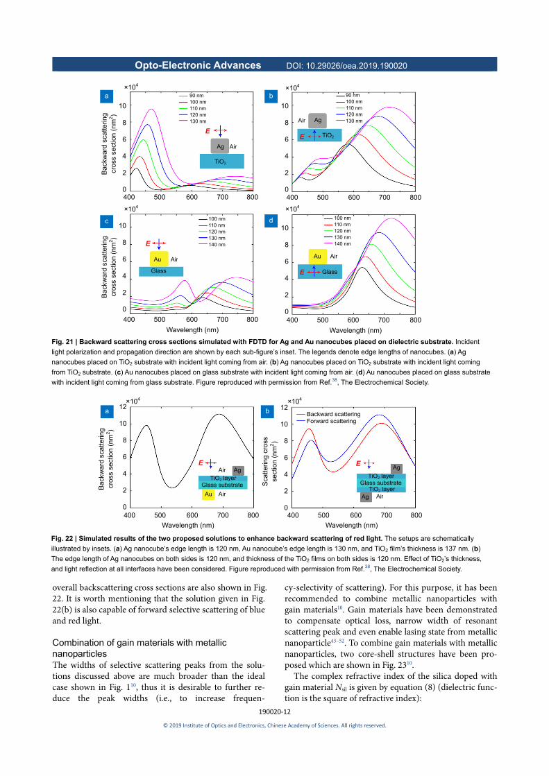
As shown in Fig. 1739, when a Ag nanocube is placed on a solid dielectric substrate, its LSPR light scattering peak splits into two modes: the distal mode (peak 1) and the proximal mode (peak 2). And it has been shown that the higher the refractive index of the substrate, the larger the distance between the two peaks39. As will be shown later, when TiO2 which has high refractive index is chosen as the substrate, the peak at lower wavelength is suitable for selective backscattering of blue light.
The resonance peak splitting of a Ag nanocube, also called Fano resonance, when it is placed on a dielectric substrate originates from the substrate-mediated coupling between a bright dipolar and a dark quadrupolar plasmon mode40,41.
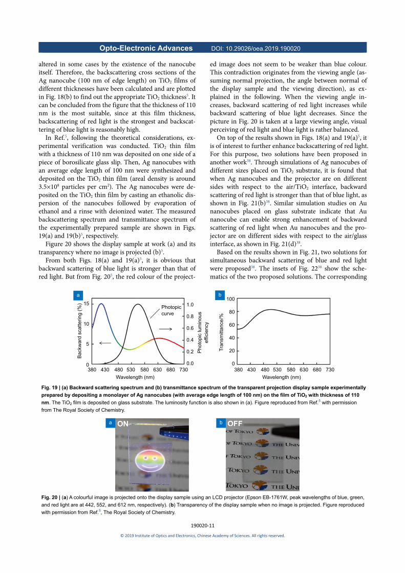
Both peak wavelength and intensity of scattering spec-trum are affected by nanoparticle’s size8,9, which is con-firmed by the results shown in Fig. 18(a)5. In this figure, the backscattering spectrums of Ag nanocubes with three different sizes (edge lengths of 80 nm, 100 nm and 120
nm) on sufficiently thick TiO2 (800 nm) were simulated using Lumerical FDTD solutions5.
Based on the results shown in Fig. 18(a)5, it can be con-cluded that Ag nanocube with a 100 nm edge length is more suitable for transparent projection display due to the following two reasons: 1. The two peak wavelengths of its scattering peaks are around 440 nm and 640 nm, re-spectively, which are more suitable for blue and red light scattering. 2. It is more difficult to synthesize nanocube of larger sizes. It is believed that enhancement of green light backscattering is not so important since human eyes are sensitive to green light (see the photopic luminous curve in Fig. 18(a)). As observed from Fig. 18(a)5, backscatter-ing of red light is much weaker compared to that of blue light, so it is desirable to enhance backscattering of red light. If more red light is reflected at the air/TiO2 interface, then more red light is expected to be scattered by Ag nanocube, and hence backscattering of red light is ex-pected to be enhanced. Reflection of red light can be in-creased by taking advantage of constructive optical inter-ference: make the red light reflected at the air/TiO2 inter-face constructively interfere with that reflected at the TiO2/glass interface (the substrate is assumed to be glass). The light intensity that the Ag nanocube receives may be
Fig. 17 | FDTD (finite-difference time-domain) simulations showing (a) a second peak emerges when a single Ag nanocube (edge
length of 90 nm) approaches a glass substrate (index assumed to be 1.5), and the near field |E| plots for (b) peak 1 and (c) peak 2 of
the nanocube placed on the glass substrate. The surrounding medium is air, and the white line in (b), (c) represent the interface between
Ag nanocube (or Air) and the glass substrate. Figure adapted with permission from Ref.39, American Chemical Society.
Fig. 18 | (a) Simulated backward scattering spectrums with FDTD for Ag nanocubes deposited on TiO2 with sufficient thickness (800 nm). The
luminosity function is also shown to indicate that human eyes are not sensitive to blue and red light. In the calculations, TiO2’s refractive index
is from Ref.42, and Ag’s refractive index is from Ref.19. (b) Calculated dependence of the distal and proximal mode backward scattering peak
intensities of a 100 nm Ag nanocube on the TiO2 thickness. Figure reproduced with permission from Ref.5, The Royal Society of Chemistry.
altered in some cases by the existence of the nanocube itself. Therefore, the backscattering cross sections of the Ag nanocube (100 nm of edge length) on TiO2 films of different thicknesses have been calculated and are plotted in Fig. 18(b) to find out the appropriate TiO2 thickness5. It can be concluded from the figure that the thickness of 110 nm is the most suitable, since at this film thickness, backscattering of red light is the strongest and backscat-tering of blue light is reasonably high.
In Ref.5, following the theoretical considerations, ex-perimental verification was conducted. TiO2 thin film with a thickness of 110 nm was deposited on one side of a piece of borosilicate glass slip. Then, Ag nanocubes with an average edge length of 100 nm were synthesized and deposited on the TiO2 thin film (areal density is around 3.5×10⁸ particles per cm2). The Ag nanocubes were de-posited on the TiO2 thin film by casting an ethanolic dis-persion of the nanocubes followed by evaporation of ethanol and a rinse with deionized water. The measured backscattering spectrum and transmittance spectrum of the experimentally prepared sample are shown in Figs. 19(a) and 19(b)5, respectively.
Figure 20 shows the display sample at work (a) and its transparency where no image is projected (b)5.
From both Figs. 18(a) and 19(a)5, it is obvious that backward scattering of blue light is stronger than that of red light. But from Fig. 205, the red colour of the project-
ed image does not seem to be weaker than blue colour. This contradiction originates from the viewing angle (as-suming normal projection, the angle between normal of the display sample and the viewing direction), as ex-plained in the following. When the viewing angle in-creases, backward scattering of red light increases while backward scattering of blue light decreases. Since the picture in Fig. 20 is taken at a large viewing angle, visual perceiving of red light and blue light is rather balanced.
On top of the results shown in Figs. 18(a) and 19(a)5, it is of interest to further enhance backscattering of red light. For this purpose, two solutions have been proposed in another work38. Through simulations of Ag nanocubes of different sizes placed on TiO2 substrate, it is found that when Ag nanocubes and the projector are on different sides with respect to the air/TiO2 interface, backward scattering of red light is stronger than that of blue light, as shown in Fig. 21(b)38. Similar simulation studies on Au nanocubes placed on glass substrate indicate that Au nanocube can enable strong enhancement of backward scattering of red light when Au nanocubes and the pro-jector are on different sides with respect to the air/glass interface, as shown in Fig. 21(d)38.
Based on the results shown in Fig. 21, two solutions for simultaneous backward scattering of blue and red light were proposed38. The insets of Fig. 2238 show the sche-matics of the two proposed solutions. The corresponding
Fig. 19 | (a) Backward scattering spectrum and (b) transmittance spectrum of the transparent projection display sample experimentally
prepared by depositing a monolayer of Ag nanocubes (with average edge length of 100 nm) on the film of TiO2 with thickness of 110
nm. The TiO2 film is deposited on glass substrate. The luminosity function is also shown in (a). Figure reproduced from Ref.5 with permission
from The Royal Society of Chemistry.
Fig. 20 | (a) A colourful image is projected onto the display sample using an LCD projector (Epson EB-1761W, peak wavelengths of blue, green,
and red light are at 442, 552, and 612 nm, respectively). (b) Transparency of the display sample when no image is projected. Figure reproduced
with permission from Ref.5, The Royal Society of Chemistry.
overall backscattering cross sections are also shown in Fig. 22. It is worth mentioning that the solution given in Fig. 22(b) is also capable of forward selective scattering of blue and red light.
Combination of gain materials with metallic nanoparticles The widths of selective scattering peaks from the solu-tions discussed above are much broader than the ideal case shown in Fig. 110, thus it is desirable to further re-duce the peak widths (i.e., to increase frequen-
cy-selectivity of scattering). For this purpose, it has been recommended to combine metallic nanoparticles with gain materials10. Gain materials have been demonstrated to compensate optical loss, narrow width of resonant scattering peak and even enable lasing state from metallic nanoparticle43–52. To combine gain materials with metallic nanoparticles, two core-shell structures have been pro-posed which are shown in Fig. 2310.
The complex refractive index of the silica doped with gain material Nsil is given by equation (8) (dielectric func-tion is the square of refractive index):
Fig. 22 | Simulated results of the two proposed solutions to enhance backward scattering of red light. The setups are schematically
illustrated by insets. (a) Ag nanocube’s edge length is 120 nm, Au nanocube’s edge length is 130 nm, and TiO2 film’s thickness is 137 nm. (b)
The edge length of Ag nanocubes on both sides is 120 nm, and thickness of the TiO2 films on both sides is 120 nm. Effect of TiO2’s thickness,
and light reflection at all interfaces have been considered. Figure reproduced with permission from Ref.38, The Electrochemical Society.
E E
Air Air
TiO2 layer
Ag
Backward scattering Forward scattering
Wavelength (nm)
400 500 600 700 800
12
10
8
6
4
2
0
×104
Ba
ckw
ard
scat
terin
g
cros
s se
ctio
n (
nm
2 )
a
Ag
Au
Glass substrate
AgTiO2 layer
Glass substrate TiO2 layer
Sca
tterin
g c
ross
se
ctio
n (
nm
2 )
12
10
8
6
4
2
0
×104 b
Air
Wavelength (nm)
400 500 600 700 800
Fig. 21 | Backward scattering cross sections simulated with FDTD for Ag and Au nanocubes placed on dielectric substrate. Incident
light polarization and propagation direction are shown by each sub-figure’s inset. The legends denote edge lengths of nanocubes. (a) Ag
nanocubes placed on TiO2 substrate with incident light coming from air. (b) Ag nanocubes placed on TiO2 substrate with incident light coming
from TiO2 substrate. (c) Au nanocubes placed on glass substrate with incident light coming from air. (d) Au nanocubes placed on glass substrate
with incident light coming from glass substrate. Figure reproduced with permission from Ref.38, The Electrochemical Society.
where i is the imaginary number, and extinction coeffi-cient k is a negative number for a gain media. Note that for a transparent material, k=0; for an absorbing material, k>0. And the relation between extinction coefficient k and optical gain is gain=–4πk/λ, where λ is the wave-length of the incident light.
With the introduction of gain, the optimization process has one more degree of freedom, i.e., apart from core diameter, shell thickness and resonant wavelength, value of k can also be tuned. The optimized results are shown in Fig. 2410.
From Fig. 2410, it is observed that even though the ef-fect of surface scattering of free electrons is considered during optimization (this effect undesirably broadens resonance peak and increases absorption level), including gain materials can achieve very sharp resonant scattering peaks. A comparison between performances of the three structures in Fig. 24 with those of their corresponding ones without gain materials is given in supplementary material to show the significant improvement of scatter-
ing performance with introduction of gain material. Thus, combining gain material with metallic nanoparticles pro-vides a promising way to achieve high frequency-selective light scattering.
Summary In this article, for the purpose of achieving transparent projection display, we have reviewed recent progress of frequency-selective scattering of red, green and blue light achieved by metallic nanoparticle’s LSPR. Method and criteria of choosing appropriate metal(s) are discussed, and it is concluded that Ag is the most suitable metal in visible wavelength range for the display application. FOM is defined to quantify the performance of a designed na-noparticle structure. Selective scattering based on spheri-cal core-shell structures are reviewed. The spherical core-shell structures have the advantage of high sym-metry, which means that they do not have the problem of alignment and special requirement on incident light. The structure of ellipsoidal Ag has better performance in terms of FOM compared to spherical core-shell structures;
Fig. 24 | Optimized results for selective scattering of red, green and blue light when gain materials are combined with metallic nanoparti-
cles. (a) Silica doped with gain material as core, Au as shell, for selective scattering of red light. (b) Silica doped with gain material as core, Ag as
shell, for selective scattering of green light. (c) Ag as core, Silica doped with gain material as shell, for selective scattering of blue light. Schematic
illustration of core-shell structures is shown in Fig. 23. Optimized parameters and values of FOM are shown in the insets. Efficiency is the corre-
sponding cross section (i.e., extinction, scattering or absorption) divided by the nanoparticle’s geometrical cross section πr2, where r is core-shell
structure’s outer radius. Simulations are done by the Mie theory12. Figure adapted with permission from Ref.10, Optical Society of America.
Fig. 23 | Proposed core-shell structures for combining metallic nanoparticle with gain material. (a) Core is metal, shell is silica doped with
gain material. (b) Core is silica doped with gain material, shell is metal. The surrounding medium’s dielectric function εs is assumed to be a constant
of 2.25. The complex refractive index of silica doped with gain material is described by equation (8). Metal could be Ag or Au. Figure adapted with
permission from Ref.10, Optical Society of America.
a Metal/Silica with gain b Silica/Metal with gain
Incident light Incident light Silica shell with gain Metal shell
εs
εm
εsil
εs
εsil
εm
Metalcore
Silica core with gain
25
20
15
10
5
0
Effi
cie
ncie
s
a b c
400 500 600 700 800
Silica/Au with gain for red Silica/Ag with gain for green Ag/Silica with gain for blue
however, due to its asymmetry, extra effort is needed for alignment of nanoparticles to ensure the device’s inde-pendence on incident light’s polarization. Super-sphere core-shell structure provides a promising way of increas-ing strength of light scattering while suppressing light absorption, but its fabrication process needs careful de-sign to precisely control its geometrical shape. The struc-ture of Ag or Au nanocubes placed on a dielectric sub-strate provides another alternative for achieving selective scattering, although FOM is not suitable to describe its performance. As the selective scattering of the above mentioned structures are not sharp enough, the combina-tion of metallic nanoparticles with gain materials is rec-ommended, which can theoretically generate very sharp scattering peaks.
Much research is still needed to realize commercially viable nanoparticles which have highly frequen-cy-selective scattering of red, green and blue light. And we would like to recommend several future works in this field:
For the three structures proposed in Fig. 24, experi-mental realization of them is worth trying.
For the idea of placing metallic nanoparticle on dielec-tric substrate, frequency-selective light scattering proper-ties have only been studied for the shape of nanocube as reviewed in Section “Metallic nanocubes”. Therefore, it is recommended that studies on other shapes, such as nano-star, nano-triangle and nano-rice may be attempted. Also, it is interesting to investigate how it will affect their light scattering and absorption properties by coating the-se nanoparticles with a thin layer of dielectric doped with gain materials. On top of these, it has been shown that when a monolayer of Molybdenum disulfide (MoS2) is inserted between the metallic nanoparticle and the die-lectric substrate, strength and spectral position of the resonance peaks can be tuned by applying different gate voltages on the MoS2 monolayer53. Therefore, the effect of MoS2 monolayer on frequency-selective light scattering properties of metallic nanoparticle deposited on dielectric substrate is worth future research.
Dielectric nanoparticles may be a promising way of achieving frequency-selective scattering of light, as they do not suffer from light absorption as compared to metal-lic nanoparticle. One example is shown in supplementary material of Ref. 4.
References 1. Jang C, Lee C K, Jeong J, Li G, Lee S et al. Recent progress in
see-through three-dimensional displays using holographic opti-
cal elements. Appl Opt 55, A71–A85 (2016).
2. Sun T, Pettitt G, Ho N T, Eckles K, Clifton B et al. Full color high
contrast front projection on black emissive display. Proc SPIE
8254, (2012).
3. Chen S F, Deng L L, Xie J, Peng L, Xie L H et al. Recent devel-
opments in top-emitting organic light-emitting diodes. Adv Mater
22, 5227–5239 (2010).
4. Hsu C W, Zhen B, Qiu W J, Shapira O, DeLacy B G et al.
Transparent displays enabled by resonant nanoparticle scatter-
ing. Nat Commun 5, 3152 (2014).
5. Saito K, Tatsuma T. A transparent projection screen based on
plasmonic Ag nanocubes. Nanoscale 7, 20365–20368 (2015).
6. Monti A, Toscano A, Bilotti F. Analysis of the scattering and ab-
sorption properties of ellipsoidal nanoparticle arrays for the de-
sign of full-color transparent screens. J Appl Phys 121, 243106
(2017).
7. Ye Y Y, Chen T P, Zhen J Y, Xu C, Zhang J et al. Resonant
scattering of green light enabled by Ag@TiO2 and its application
in a green light projection screen. Nanoscale 10, 2438–2446
(2018).
8. Kreibig U, Vollmer M. Optical Properties of Metal Clusters
(Springer, Berlin, Heidelberg, 2013).
9. Kelly K L, Coronado E, Zhao L L, Schatz G C. The optical prop-
erties of metal nanoparticles: the influence of size, shape, and
dielectric environment. J Phys Chem B 107, 668–677 (2003).
10. Ye Y Y, Liu R Y, Song Z G, Liu Z, Chen T P. Sharp selective
scattering of red, green, and blue light achieved via gain materi-
al's loss compensation. Opt Express 27, 9189–9204 (2019).
11. Kreibig U. Small silver particles in photosensitive glass: their
nucleation and growth. Appl Phys 10, 255–264 (1976).
12. Quinten M. Optical Properties of Nanoparticle Systems: Mie and
Beyond (John Wiley & Sons, Weinheim, 2011).
13. Yang W. Improved recursive algorithm for light scattering by a
36. Miyazawa T, Aratake M, Onaka S. Superspherical-shape ap-
proximation to describe the morphology of small crystalline par-
ticles having near-polyhedral shapes with round edges. J Math
Chem 50, 249–260 (2012).
37. Saito K, Tatsuma T. Asymmetric three-way plasmonic color
routers. Adv Opt Mater 3, 883–887 (2015).
38. Ye Y Y, Chen T P. Selective scattering of blue and red light
based on silver and gold nanocubes. ECS J Solid State Sci
Technol 8, R51–R57 (2019).
39. Sherry L J, Chang S H, Schatz G C, Van Duyne R P, Wiley B J
et al. Localized surface plasmon resonance spectroscopy of
single silver nanocubes. Nano Lett 5, 2034–2038 (2005).
40. Davis T J, Gómez D E, Vernon K C. Simple model for the hy-
bridization of surface plasmon resonances in metallic nanoparti-
cles. Nano Lett 10, 2618–2625 (2010).
41. Fang Z Y, Zhu X. Plasmonics in nanostructures. Adv Mater 25,
3840–3856 (2013).
42. Jellison G E Jr, Boatner L A, Budai J D, Jeong B S, Norton D P.
Spectroscopic ellipsometry of thin film and bulk anatase (TiO2). J
Appl Phys 93, 9537–9541 (2003).
43. Avrutsky I. Surface plasmons at nanoscale relief gratings be-
tween a metal and a dielectric medium with optical gain. Phys
Rev B 70, 155416 (2004).
44. Noginov M A, Zhu G, Bahoura M, Adegoke J, Small C E et al.
Enhancement of surface plasmons in an Ag aggregate by opti-
cal gain in a dielectric medium. Opt Lett 31, 3022–3024 (2006).
45. Digonnet M J F. Rare-Earth-Doped Fiber Lasers and Amplifiers
2nd ed (CRC Press, New York, 2001).
46. Lawandy N M. Localized surface plasmon singularities in ampli-
fying media. Appl Phys Lett 85, 5040 (2004).
47. Hide F, Schwartz B J, Díaz-García M A, Heeger A J. Conjugated
polymers as solid-state laser materials. Synth Met 91, 35–40
(1997).
48. Gordon J A, Ziolkowski R W. The design and simulated perfor-
mance of a coated nano-particle laser. Opt Express 15,
2622–2653 (2007).
49. Li X F, Yu S F. Design of low-threshold compact Au-nanoparticle
lasers. Opt Lett 35, 2535–2537 (2010).
50. Campbell S D, Ziolkowski R W. Impact of strong localization of
the incident power density on the nano-amplifier characteristics
of active coated nano-particles. Opt Commun 285, 3341–3352
(2012).
51. Zhang H P, Zhou J, Zou W B, He M. Surface plasmon amplifica-
tion characteristics of an active three-layer nanoshell-based
spaser. J Appl Phys 112, 074309 (2012).
52. Wu D J, Cheng Y, Wu X W, Liu X J. An active metallic
nanomatryushka with two similar super-resonances. J Appl Phys
116, 013502 (2014).
53. Li B W, Zu S, Zhou J D, Jiang Q, Du B W et al. Sin-
gle-nanoparticle plasmonic electro-optic modulator based on
MoS2 monolayers. ACS Nano 11, 9720–9727 (2017).
Acknowledgements This work is financially supported by National Research Foundation of Sin-gapore (NRF-CRP13-2014-02) and Science and Technology Program of Guangdong Province of China (Project No. 2016A050502058).
Author contributions All authors commented on the manuscript. Ye wrote the manuscript. Liu partially contributed to writing of manuscript and helped to revise the man-uscript. Chen guided this study and helped to revise the manuscript.
Competing interests The authors declare no competing financial interests.
Supplementary information Supplementary information for this paper is available at https://doi.org/10.29026/oea.2019.190020