Page 1
Peter Kinget
0.5V Analog integrated circuits for nanoscale CMOS technologies
Department of Electrical Engineering
Collaborators: Shouri Chatterjee, Yannis Tsividis, K.P. Pun*
[email protected]
*Chinese University of Hong Kong
Page 2
© Peter Kinget 2
Ultra-low voltage circuits: 0.5V
RF integratedoscillators
Ultra-widebandRF circuits
Injection lockedcircuits
RF Passives Device mismatch & its influence onAnalog & RF ICs
www.ee.columbia.edu/~kinget
Page 3
© Peter Kinget 3
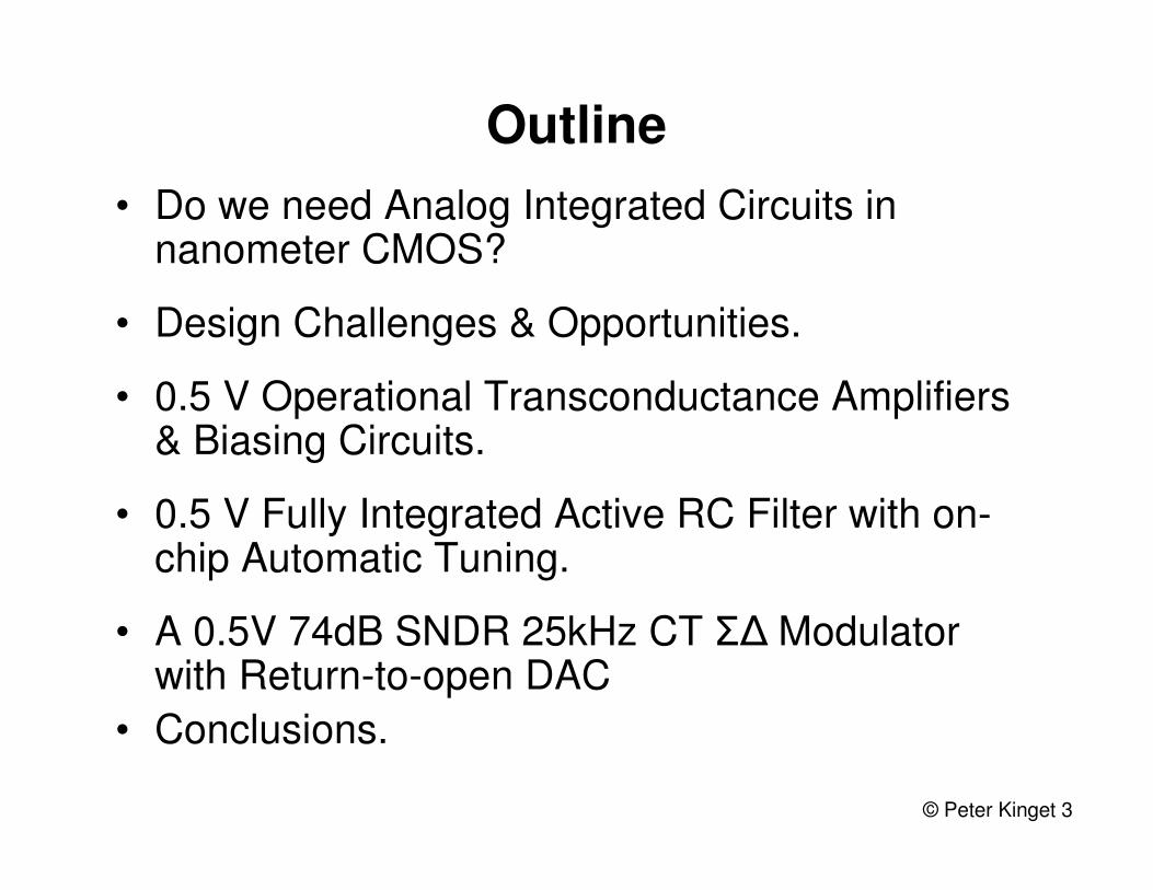
Outline
• Do we need Analog Integrated Circuits in nanometer CMOS?
• Design Challenges & Opportunities.
• 0.5 V Operational Transconductance Amplifiers & Biasing Circuits.
• 0.5 V Fully Integrated Active RC Filter with on-chip Automatic Tuning.
• A 0.5V 74dB SNDR 25kHz CT Σ∆ Modulator with Return-to-open DAC
• Conclusions.
Page 4
© Peter Kinget 4
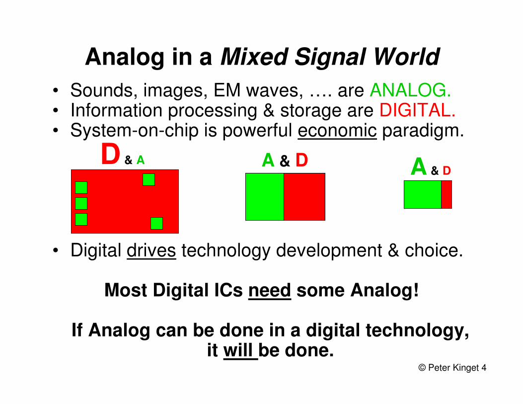
Analog in a Mixed Signal World
• Sounds, images, EM waves, …. are ANALOG.• Information processing & storage are DIGITAL.• System-on-chip is powerful economic paradigm.
• Digital drives technology development & choice.
Most Digital ICs need some Analog!
If Analog can be done in a digital technology, it will be done.
D & A A & D A & D
Page 5
© Peter Kinget 5
CMOS trends: Supply voltage
Analog VDD
Digital VDD
Digital VT
Technology node [nm]
[ITRS'04]
–O– High Perf.
–∆– Low Standby–V– Low Power
Page 6
© Peter Kinget 6
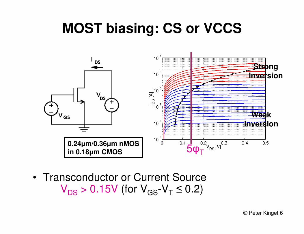
MOST biasing: CS or VCCS
• Transconductor or Current SourceVDS > 0.15V (for VGS-VT ≤ 0.2)
WeakInversion
StrongInversion
0.24µm/0.36µm nMOSin 0.18µm CMOS 5φT
Page 7
© Peter Kinget 7
Switches at 0.5 V
Large VDD
Small VDD
Enough headroom
No headroom
Page 8
© Peter Kinget 8
Common source amplifier
0.15 V
0.15 V
0.2 Vpp
0.5 + 0.15 V
0.5 V
VT= 0.5 V VDS,sat= 0.15 V
Page 9
© Peter Kinget 9
Common drain buffer
0.15 V
0.15 V
0.2 Vpp
0.5 + 0.15 + 0.1 + 0.15 V
0.5 V
VT= 0.5 V VDS,sat= 0.15 V
Page 10
© Peter Kinget 10
Common gate amplifier / Cascode
0.15 V
0.15 V0.5 + 0.15 +
x + 0.15 V
0.5 V
VT= 0.5 V VDS,sat= 0.15 V
0.15 V
Page 11
© Peter Kinget 11
Differential OTA design challenges
0.15 V
0.5 V
0.65 V
0.8 V
-0.15 V
0.15 V
0.15 V
0.3 - 0.35 V
0.5 V
0.1 V
0.4 V0.4 V
0.1 V
0.15 - 0.35 V
0.4 V
0.25 V
VT= 0.5 V VDS,sat= 0.15 V
Page 12
© Peter Kinget 12
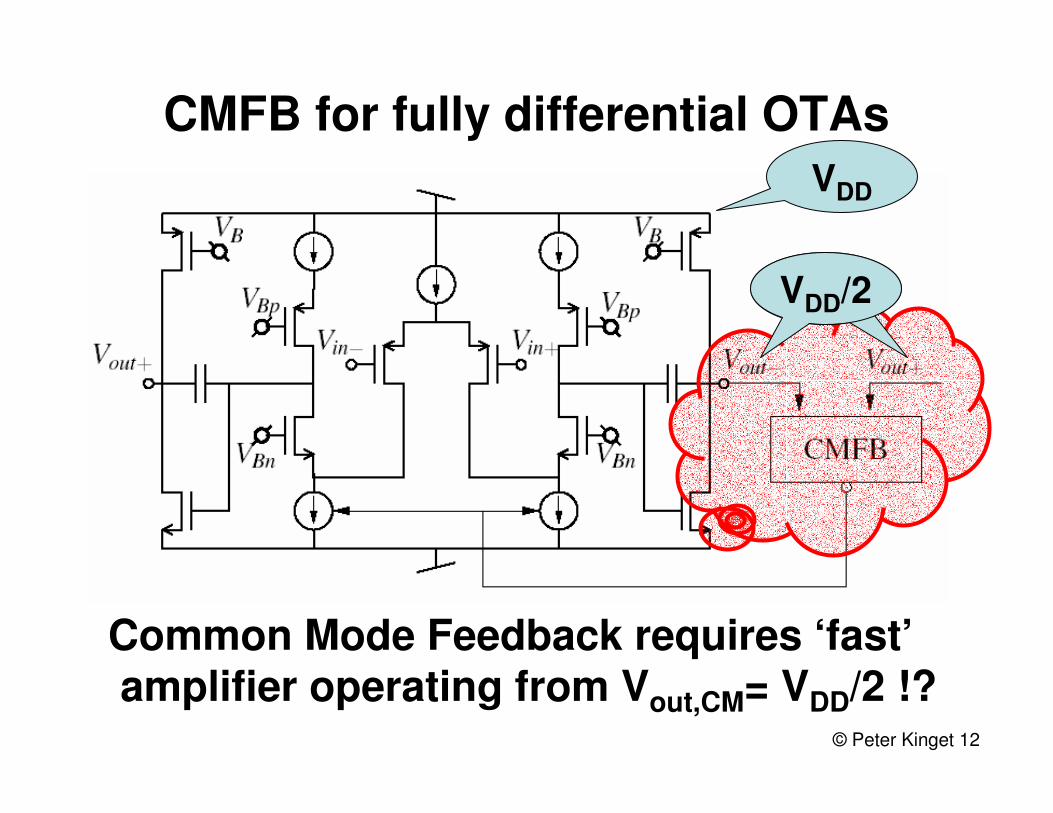
CMFB for fully differential OTAs
Common Mode Feedback requires ‘fast’ amplifier operating from Vout,CM= VDD/2 !?
VDD
VDD/2
Page 13
© Peter Kinget 13
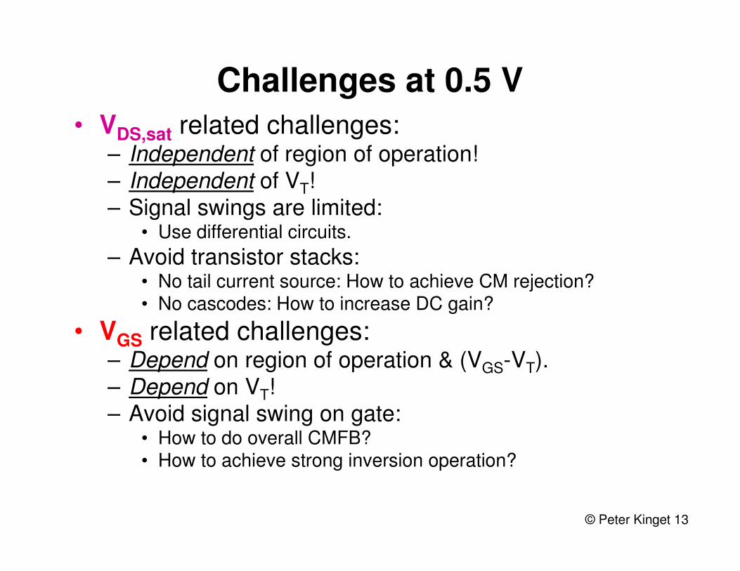
Challenges at 0.5 V
• VDS,sat related challenges:– Independent of region of operation!– Independent of VT!– Signal swings are limited:
• Use differential circuits.
– Avoid transistor stacks:• No tail current source: How to achieve CM rejection?• No cascodes: How to increase DC gain?
• VGS related challenges:– Depend on region of operation & (VGS-VT).– Depend on VT!– Avoid signal swing on gate:
• How to do overall CMFB?• How to achieve strong inversion operation?
Page 14
© Peter Kinget 14
Opportunities at 0.5 V: MOST has 4-terminals
Body
Source
Drain
Gate
G D BS Sub
n+
n+n+n+ n+
p+ p+
p
p
nMOS cross section(deep n-well process)
nMOS circuit equivalent(deep n-well process)
VDD
VDD
Page 15
© Peter Kinget 15
Opportunities at 0.5 V
• Body terminal
– Signal input: [Guz87]
– VT reduction & control
[Kob94], [Von94]
– Bias control
• Latch-up not an issue
– Assuming VDD and GND are ‘well behaved’.
• Techniques can be ported to ‘double gate’ devices
VBS0.5 V
500
0
VT
mV
300
430360
0.0
VGS0.5 V0.2
3
0
IDS VBS ↑
µA
0.24µm/0.36µm nMOSin 0.18µm CMOS
Page 16
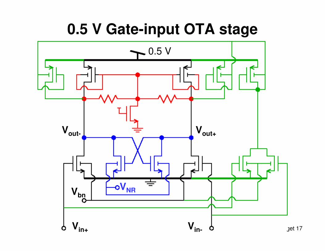
0.5 V Gate-input OTA
Page 17
© Peter Kinget 17
0.5 V Gate-input OTA stage
Vin+ Vin-
Vout+Vout-
VbnVNR
0.5 V
Page 18
© Peter Kinget 18
Two stage OTA
• Common-mode output of first stage is 0.4 V
0.25 V
0.4 V
0.4 V
Page 19
© Peter Kinget 19
Two-stage fully differential 0.5 V OTA with Miller compensation
Page 20
© Peter Kinget 20
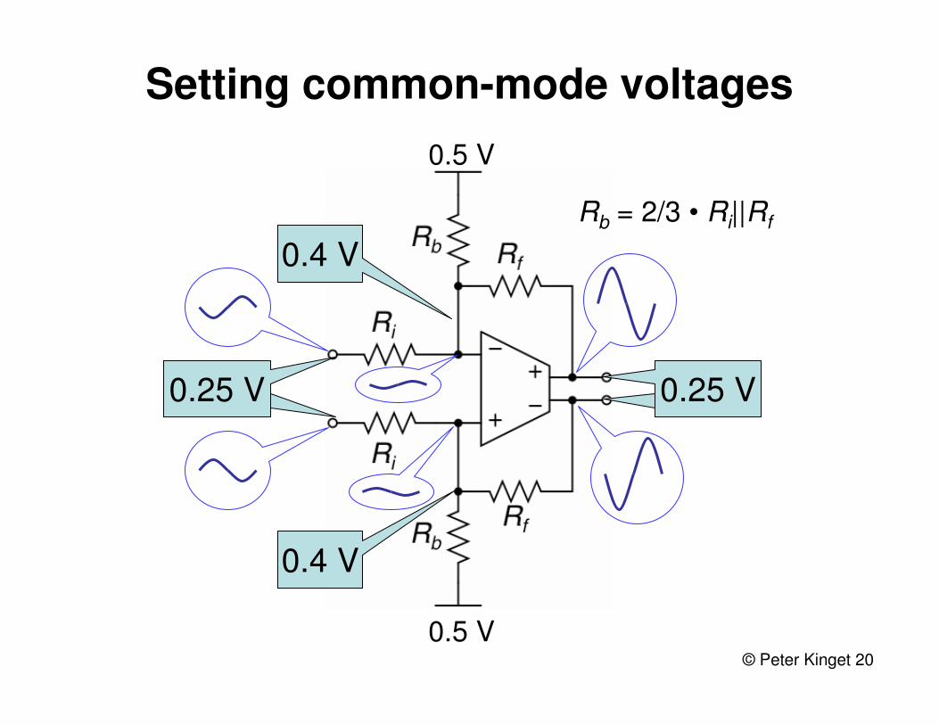
Setting common-mode voltages
0.5 V
0.4 V
0.4 V
0.5 V
Rb = 2/3 • Ri||Rf
0.25 V 0.25 V
Page 21
© Peter Kinget 21
Open loop performance (meas.)G
ain
[d
B]
42 dB
GBW: 10 MHz
CL= 10pF (diff.)RL= 50kΩIDD= 150 µA
62 dB 350mV; automatic bias
Frequency [Hz]
Page 22
On-chip automatic biasing circuits
Page 23
© Peter Kinget 23
On-chip biasing circuits
Vbn generating circuit
Level shift biasing circuit
(Simplified OTA)
Page 24
© Peter Kinget 24
Error amplifier for biasing
• 20 kHz GBW for 1 pF load
• 2 µA current• Controlled body voltage sets the amplifier threshold
VinVout
Vo
ut[V
]
Vin [V]
Page 25
© Peter Kinget 25
OTA DC transfer characteristics and VNR generation
VNR generating circuit
Replica of OTA stage 1
Input differential voltage [mV]
Ou
tpu
t d
iff vo
lta
ge
[V
]
Increasing VNR
Page 26
© Peter Kinget 26
Open loop performance (meas.)G
ain
[d
B]
42 dB
GBW: 10 MHz
CL= 10pF (diff.)RL= 50kΩIDD= 150 µA
62 dB 350mV; automatic bias
Frequency [Hz]
Page 27
0.5 V Continuous time
tunable active RC Filter
Page 28
© Peter Kinget 28
0.5 V 5th order elliptic LPF
Frequency [Hz]
Ga
in [
dB
]
280 kHz
135 kHz
Page 29
© Peter Kinget 29
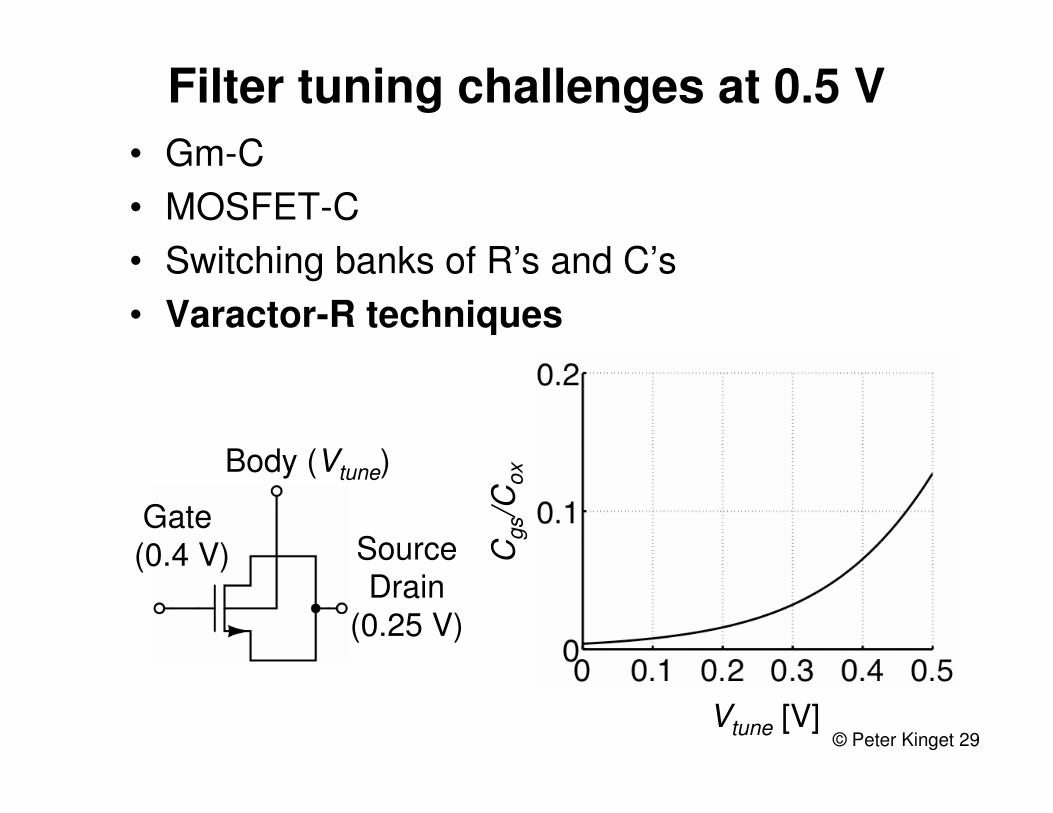
Filter tuning challenges at 0.5 V
• Gm-C
• MOSFET-C
• Switching banks of R’s and C’s
• Varactor-R techniques
Vtune [V]
Cg
s/C
ox
Gate (0.4 V) Source
Drain (0.25 V)
Body (Vtune)
Page 30
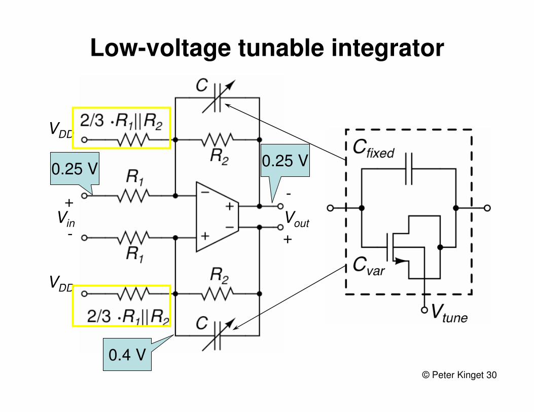
© Peter Kinget 30
Low-voltage tunable integrator
0.25 V0.25 V
0.4 V
+
-Vin Vout
+
-
VDD
VDD
Page 31
© Peter Kinget 31
Die photograph
• 0.18 µm CMOS
• MIM capacitors
• High-res resistors
• Standard VT
• Triple well devices
Filter PLL
Biasing circuits
OTAs
1mm
1m
m
S. Chatterjee, Y. Tsividis, and P. Kinget, "A 0.5 V filter with PLL-based tuning in 0.18 um CMOS technology," in IEEE International Solid-State Circuits Conference (ISSCC), pp. 506-507, February 2005.
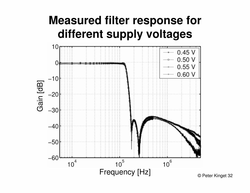
Page 32
© Peter Kinget 32Frequency [Hz]
Ga
in [
dB
]
Measured filter response for different supply voltages
Page 33
© Peter Kinget 33
Measured filter response for different chips
Frequency [Hz]
Ga
in [
dB
]
1.3 % std dev
in cut-off frequency for 20 samples
Page 34
© Peter Kinget 34
Measured filter response for different tuning voltages
Frequency [Hz]
Ga
in [
dB
]
88 - 154 kHz(1.75x)
Page 35
© Peter Kinget 35
Measured 3rd order inter-modulation
25 kHz
20 kHz
15 kHz
30 kHz
40 dB
Input differential rms amplitude [V]
Ou
t pu
t d
iffe
ren
tia
l rm
s a
mp
litu
de
[V
]
Page 36
Effect of gain enhancement
Frequency [Hz]
Ga
in [
dB
]
Without gain-enhancement
With gain-enhancement
Page 37
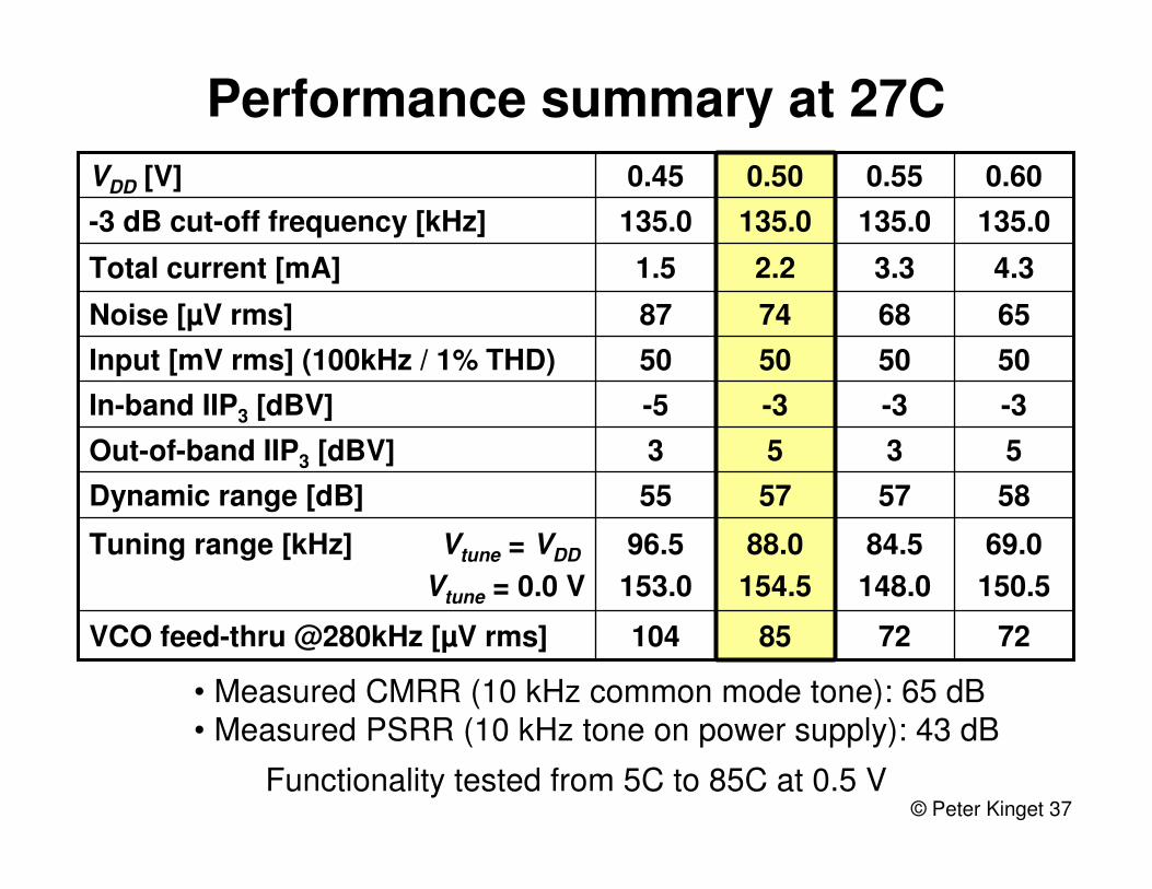
© Peter Kinget 37
Performance summary at 27C
727285104VCO feed-thru @280kHz [µV rms]
69.0
150.5
84.5
148.0
88.0
154.5
96.5
153.0
Tuning range [kHz] Vtune = VDD
Vtune = 0.0 V
58575755Dynamic range [dB]
5353Out-of-band IIP3 [dBV]
-3-3-3-5In-band IIP3 [dBV]
50505050Input [mV rms] (100kHz / 1% THD)
65687487Noise [µV rms]
4.33.32.21.5Total current [mA]
135.0135.0135.0135.0-3 dB cut-off frequency [kHz]
0.600.550.500.45VDD [V]
Functionality tested from 5C to 85C at 0.5 V
• Measured CMRR (10 kHz common mode tone): 65 dB• Measured PSRR (10 kHz tone on power supply): 43 dB
Page 38
0.5 V Body-input OTA
Page 39
© Peter Kinget 39
0.5 V Body-input OTA stage
0.5 V
Vin+ Vin-
Vout+Vout-
0.25 V
0.15 - 0.35 V
0.07 V
0.25 V
Page 40
© Peter Kinget 40
Two-stage fully-differential OTA
0.18 µµµµm CMOS
Pole splitting using Miller capacitor
S. Chatterjee, Y. Tsividis, and P. Kinget, "A 0.5 V bulk input fully differential operational transconductance amplifier," in European Solid-State Circuits Conference (ESSCIRC), pp.147-150, September 2004.
Page 41
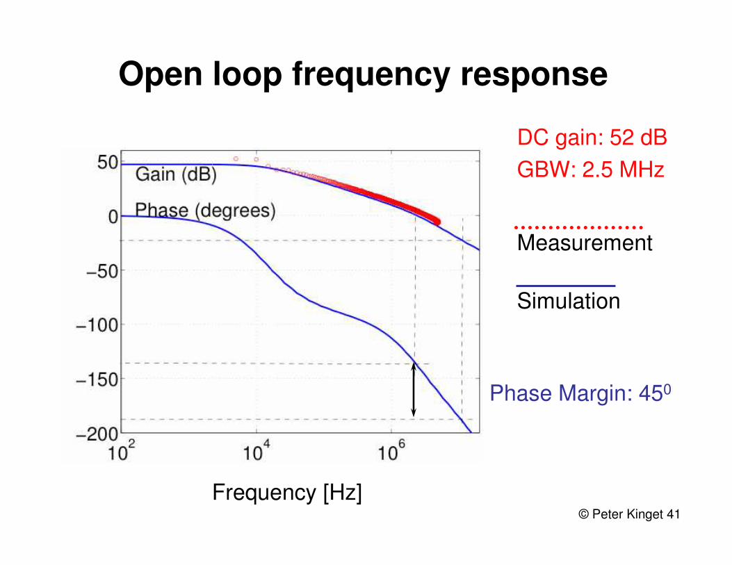
© Peter Kinget 41
Open loop frequency response
DC gain: 52 dB
GBW: 2.5 MHz
Phase Margin: 450
Frequency [Hz]
Simulation
Measurement
Page 42
© Peter Kinget 42
66.711.413289.5100 η [1/V]
----Depl.MOS
Lat.BJT
-Lat.BJT
SpecialDevices
0.180.180.50.72.50.50.352Techn. [um]
DDDSSSSSSE/Diff.
101014-1220722CL [pF]
75110-4600.5-5300Power [uW]
102.541.36e-31.30.21.3GBW [MHz]
50/6252598470537049ADC [dB]
0.50.50.91.30.90.811VDD [V]
G-IB-I[Pel98]
[Fer96]
[Sto02]
[Leh01]
[Las00]
[Bla98]
S. Chatterjee, Y. Tsividis and P. Kinget, "0.5 V Analog Circuit
Techniques and Their Application in OTA and Filter Design," IEEE
Journal of Solid-State Circuits (JSSC), vol. 40, no 12, pp. 2373 -
2387, December 2005.
Page 43
A 0.5V 74dB SNDR 25kHz CT Σ∆ Modulator
with Return-to-open DAC
Page 44
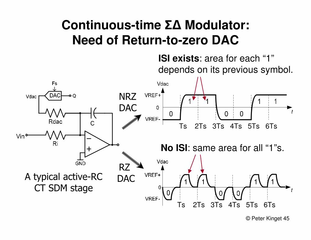
© Peter Kinget 44
3rd order CT Σ∆ Modulator
Using Active RC integrators
Page 45
© Peter Kinget 45
Ts 2Ts 3Ts 4Ts 5Ts 6Ts
Ts 2Ts 3Ts 4Ts 5Ts 6Ts
Continuous-time Σ∆ Modulator:Need of Return-to-zero DAC
NRZ DAC
RZ DACA typical active-RC
CT SDM stage
ISI exists: area for each “1”depends on its previous symbol.
No ISI: same area for all “1”s.
Page 46
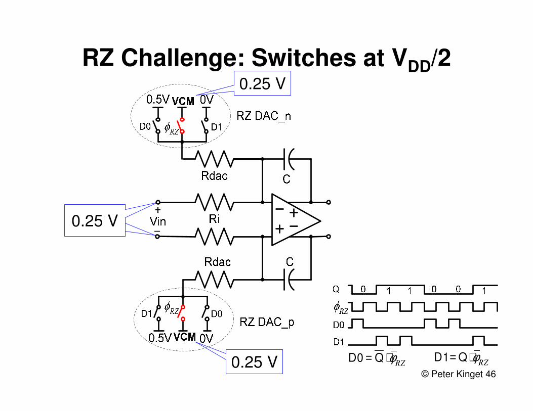
© Peter Kinget 46
RZ Challenge: Switches at VDD/2
RZφ⋅= QD0
RZφ⋅= QD1
0.25 V
0.25 V
0.25 V
Page 47
© Peter Kinget 47
Solution: Return-to-open
Before RZ:(Q=1)
v2
v1
v1
v2
Problemswitchesremoved
Page 48
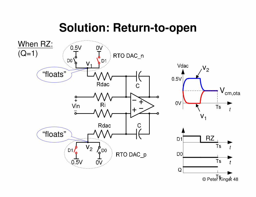
© Peter Kinget 48
Solution: Return-to-open
“floats”
v2
v2
v1
Vcm,ota
v1
When RZ:(Q=1)
“floats”RZ
Page 49
© Peter Kinget 49
Solution: Return-to-open
“floats”
v2
v2
v1
Vcm,ota
v1
When RZ:(Q=1)
“floats”
0.25 V
RZ
Page 50
© Peter Kinget 50
RTO SDM: Inter-stage Coupling
RTO DAC
Unwanted signal paths when DAC floats
Page 51
© Peter Kinget 51
Split RTO SDM Architecture
Split RTO DAC
Page 52
© Peter Kinget 52
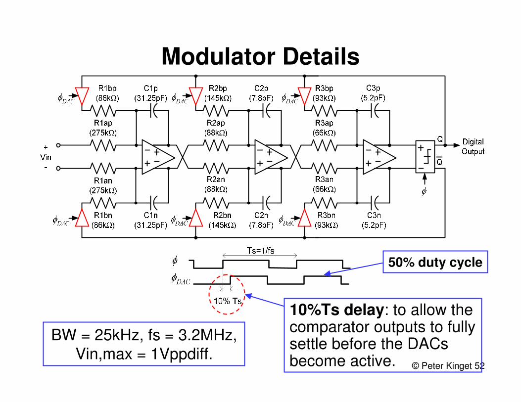
Modulator Details
50% duty cycle
BW = 25kHz, fs = 3.2MHz, Vin,max = 1Vppdiff.
10%Ts delay: to allow the comparator outputs to fully settle before the DACsbecome active.
Page 53
© Peter Kinget 53
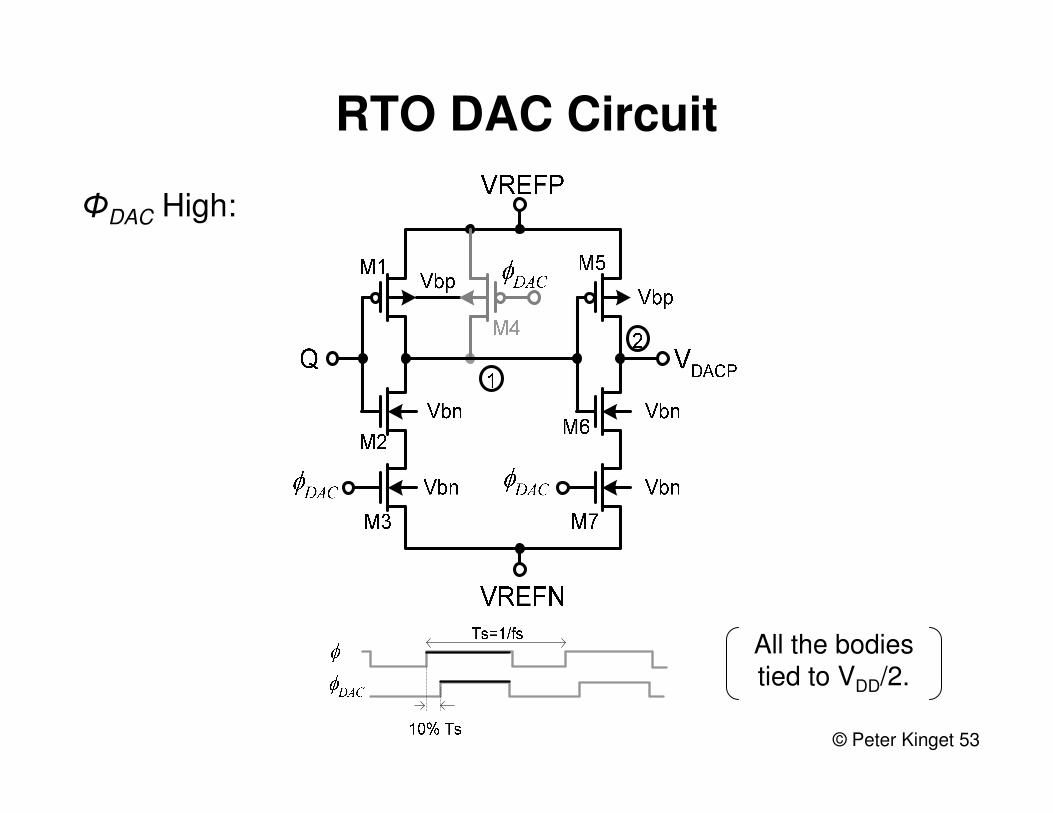
RTO DAC Circuit
ΦDAC High:
All the bodies tied to VDD/2.
Page 54
© Peter Kinget 54
RTO DAC Circuit
ΦDAC Low:
Floating.
All the bodies tied to VDD/2.
Page 55
© Peter Kinget 55
RTO DAC Circuit
ΦDAC Low:
Q invalid for Φ low.
Floating.
All the bodies tied to VDD/2.
Page 56
© Peter Kinget 56
RTO DAC Circuit
ΦDAC Low:
Make charge-injection signal-independent.
Q invalid for Φ low.
Floating.
All the bodies tied to VDD/2.
Page 57
© Peter Kinget 57
RTO DAC CircuitJust split M5-M7 for each FB path.
All the bodies tied to VDD/2.
Page 58
© Peter Kinget 58
34.534.534.534.5 35353535 35.535.535.535.5 36363636-0.1-0.1-0.1-0.1
0000
0.10.10.10.1
0.20.20.20.2
0.30.30.30.3
0.40.40.40.4
0.50.50.50.5
T ime [us]T ime [us]T ime [us]T ime [us]
DA
C O
utp
ut
Vo
lta
ge
[V
]D
AC
Ou
tpu
t V
olt
ag
e [
V]
DA
C O
utp
ut
Vo
lta
ge
[V
]D
AC
Ou
tpu
t V
olt
ag
e [
V]
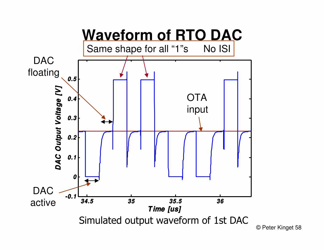
Waveform of RTO DAC
Simulated output waveform of 1st DAC
Same shape for all “1”s à No ISI
OTAinput
DACfloating
DACactive
Page 59
© Peter Kinget 59
0.5V Body-input Gate-clocked Comparator
Page 60
© Peter Kinget 60
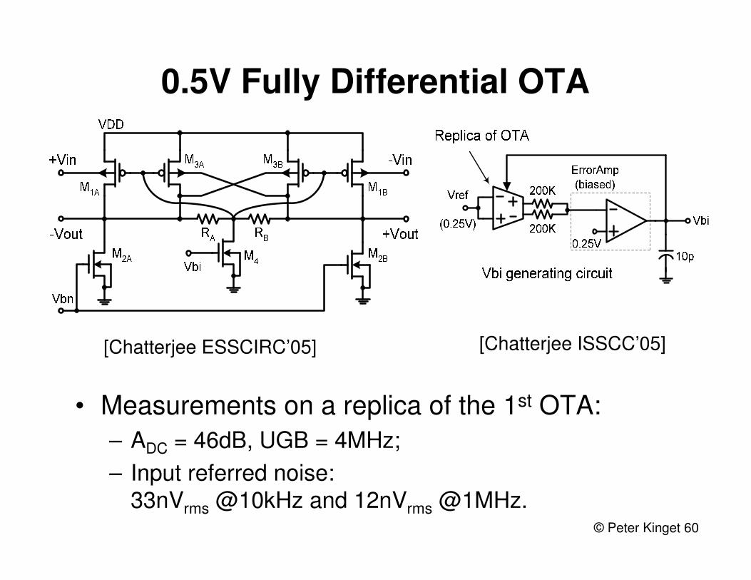
0.5V Fully Differential OTA
• Measurements on a replica of the 1st OTA:
– ADC = 46dB, UGB = 4MHz;
– Input referred noise: 33nVrms @10kHz and 12nVrms @1MHz.
[Chatterjee ESSCIRC’05] [Chatterjee ISSCC’05]
Page 61
© Peter Kinget 61
Die Photograph
• 0.18µm CMOS
• Standard VT (0.5V)
• Triple-well devices
• 0.5V operation
K.P. Pun, S. Chatterjee, and P. Kinget, "A 0.5 V 74dB SNDR 25kHz CT Delta-Sigma Modulator with Return-to-Open DAC" in IEEE International Solid-State Circuits Conference (ISSCC), pp. 72-73, February 2006.
Page 62
© Peter Kinget 62
Measured Output Spectrum
@Vin = -4dB Vref, fin = 5kHz(Vref =1Vppdiff.)
101
102
103
104
105
106
−140
−120
−100
−80
−60
−40
−20
0
Frequency [Hz]
Mag
nitu
de [d
B]
No. of points = 64000
-140
-120
-100
-80
-60
-40
-20
0
10 100 1K 10K 100K 1M
FFT points = 64000Res. BW = 50 Hz
Frequency [Hz]
Po
we
r S
pe
ctr
al D
en
sity [
dB
/bin
]
2nd harmonic < 83dBc3rd harmonic < 88dBc
Page 63
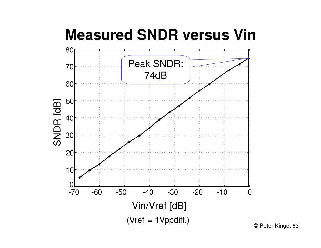
© Peter Kinget 63
Vin/Vref [dB]
SN
DR
[d
B]
−70 −60 −50 −40 −30 −20 −10 00
10
20
30
40
50
60
70
80
Vin/Vref [dB]
SN
DR
[dB
]
0
10
20
30
40
50
60
70
80
-70 -60 -50 -40 -30 -20 -10 0
Measured SNDR versus Vin
(Vref = 1Vppdiff.)
Peak SNDR:74dB
Page 64
© Peter Kinget 64
Performance Summary at 25°°°°C
0.6 mm2Active die area
370 µµµµW
300 µµµµW
70 µµµµW
0.8V0.5V0.45VSupply Voltage
76 dB
74 dB
0.18 µm CMOS
(standard VT, triple-well, MIM, and HiRes Poly)
76 dB
71 dB
1 Vppdiff.
3.2 MHz / 64
25 kHz
1-bit, 3rd order, continuous-time
74 dB
74 dB
Technology
Power consumption (total)
Sigma Delta Modulator
(filter + comparator + DAC)
Output buffers
SNR @ Vin = 1Vppdiff.
SNDR @ Vin = 1Vppdiff.
Input range
Sampling frequency / OSR
Signal bandwidth
Modulator type
Page 65
© Peter Kinget 65
SNDR versus VDD
@25°°°°C and Vin = 1Vppdiff.
Power supply voltage [V]
SN
R o
r S
ND
R [
dB
]
Page 66
© Peter Kinget 66
Temperature [°°°°C]
SN
R o
r S
ND
R [
dB
]
SNDR versus Temperature
@VDD= 0.5V and Vin = 1Vppdiff.
Page 67
© Peter Kinget 67
Performance Comparison
3400.180.63002574CT0.5This work
138Low VT0.352.8810002477SRC0.6Ahn 2005
580.180.08280867SO0.7Sauerbrey 2002
4100.50.85401662SO0.9Peluso 1998
3660.130.121500192050.9CT0.9Ueno 2004
13100.090.181402081SC1Yao 2004
381Gate
boost
0.350.639502585SC1Dessouky 2000
36Low VT0.52.53156019251CT1Matuya 1994
230.350.4156002078RO1Keskin 2001
1.30.80.9**15003.956*SO1Grech 1999
FOM[109/J]
CMOS [um]
Area[mm2]
Power[uW]
Bandwidth[kHz]
SNDR[dB]
TypeVDD[V]
*=SNR only; ** Estimated from die photograph;
SO = Switched Opamp; CT = Continuous Time;
SC = Switched Capacitor; RO = Reset Opamp;
SRC=Switched-RC
P
BWresolutionFOM ×=
Page 68
© Peter Kinget 68
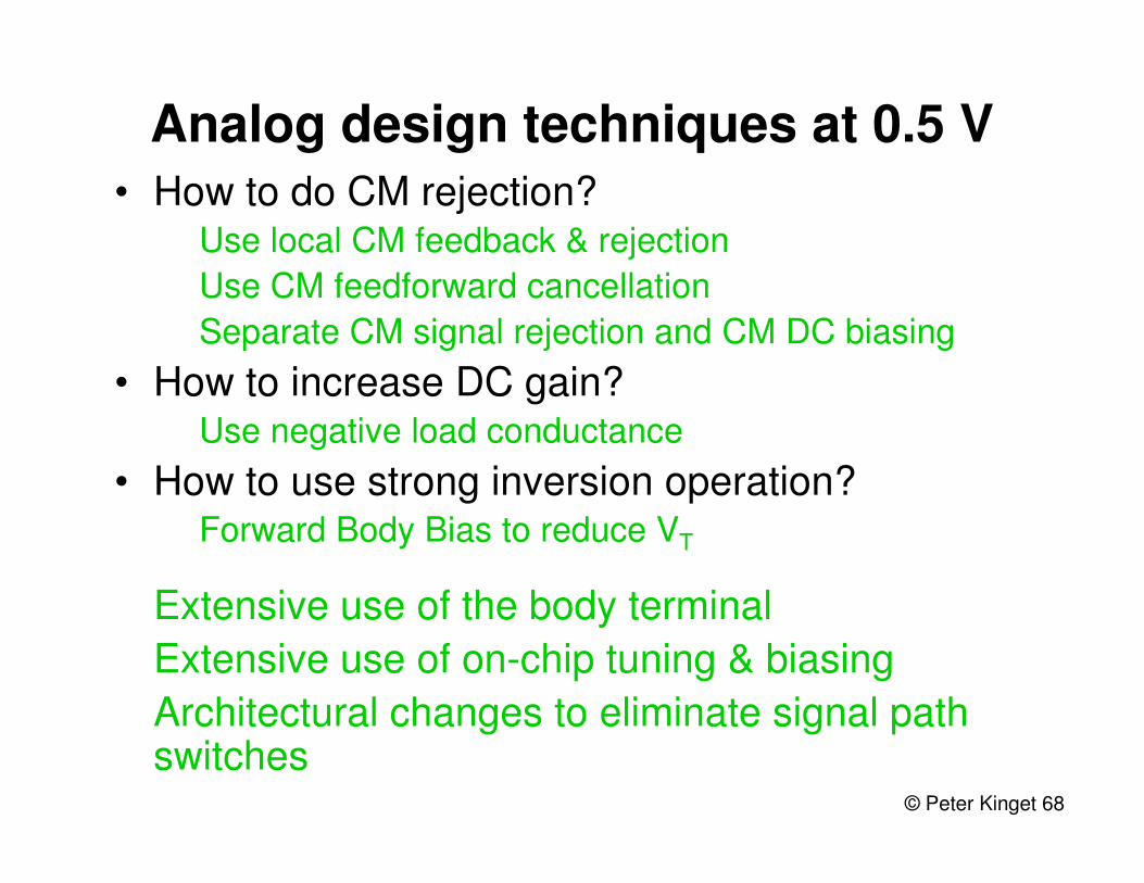
Analog design techniques at 0.5 V
• How to do CM rejection?ü Use local CM feedback & rejection
ü Use CM feedforward cancellation
ü Separate CM signal rejection and CM DC biasing
• How to increase DC gain?ü Use negative load conductance
• How to use strong inversion operation?ü Forward Body Bias to reduce VT
ü Extensive use of the body terminal
ü Extensive use of on-chip tuning & biasing
ü Architectural changes to eliminate signal path switches
Page 70
© Peter Kinget 70
0.5V 900MHz RF Front-end
• 0.18 µm CMOS
• Low-VT devices
• LNA/MIXER
– NF 8.8 dB
– Gain 11.5 or-7 dB
– ICP -23 dBm
– 5 mW(w/ LO Buffers)
LNA Mixer
Buffers
and
N. Stanic, P. Kinget, and Y. Tsividis,"A 0.5 V 900 MHz CMOS Receiver Front End,"IEEE Symposium on VLSI circuits, June 2006.
Page 71
© Peter Kinget 71
0.5 V 1 Msps 60 dB SNDR Track&Hold
First track
and hold
Second track
and hold
Bias circuits
• 0.25 µm CMOS
• |VT|=0.6V
• MIM caps• High-res resistors• Triple well nMOS
S. Chatterjee, and P. Kinget, "A 0.5-V 1-Msample/s 60-dB SNDR Track-and-Hold
Circuit," IEEE Symposium on VLSI circuits, June 2006
Page 72
© Peter Kinget 72
0.5V Analog Roadmap
2004 2005 2006
Body-input OTA
Gate-input OTA & Biasing
0.5V Varactor
THA
LPF + Tuning
∆Σ Converter
2007
RF Front-ends
DT ∆Σ Converter
Basic blocks
Full Interface
Complexity
Comparators
Page 73
© Peter Kinget 73
Other Challenges in nanometer CMOS
• Gate leakage.
• Sub-threshold leakage.
• Reduced body-effect [VonAmin05]: VT Œ & tox Œ ð gmb Œ
• Many VT choices !
• Novel devices.
• Extensive Digital Calibration & Correction.
Other Opportunities in nanometer CMOS
Page 74
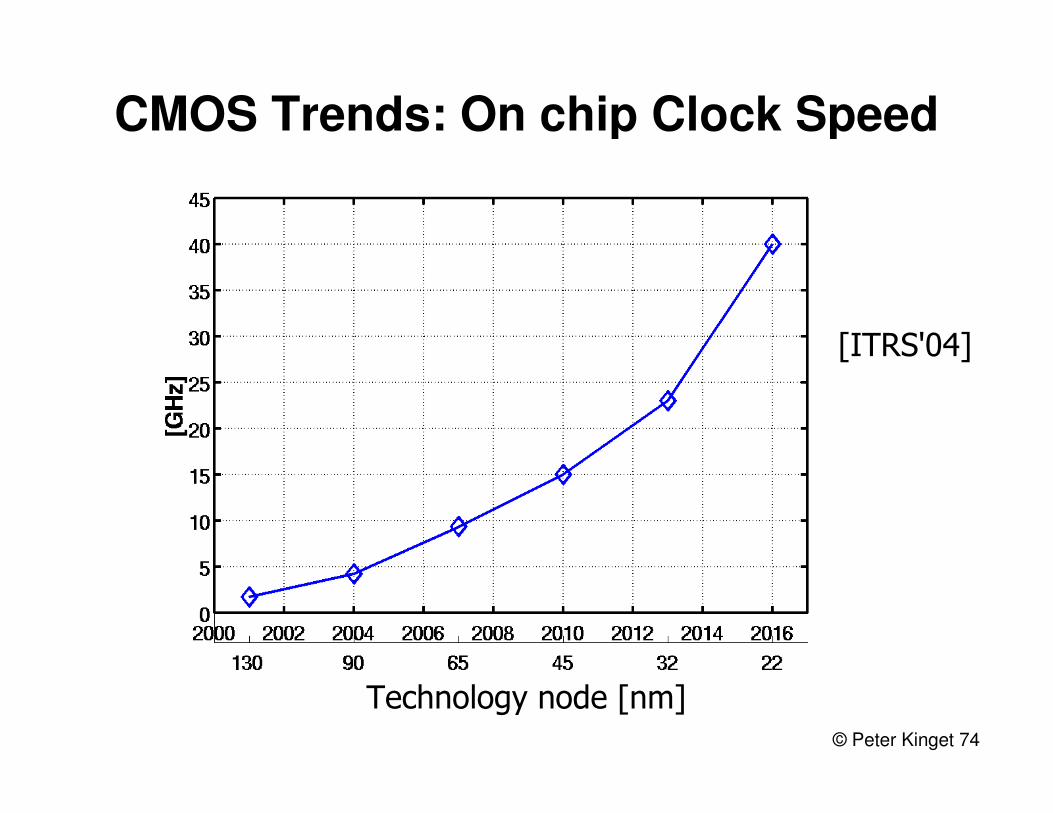
© Peter Kinget 74
CMOS Trends: On chip Clock Speed
[ITRS'04]
Technology node [nm]
Page 75
© Peter Kinget 76
Acknowledgments
• Analog Devices, Intel and Realtek for supporting parts of this work.
• Europractice and Philips Semiconductors for 0.18um and 0.25um prototypes fabrication.
Page 76
© Peter Kinget 77
More details• [Cha 05] S. Chatterjee, Y. Tsividis, and P. Kinget, "A 0.5 V filter with PLL-
based tuning in 0.18 um CMOS technology," in IEEE International Solid-State Circuits Conference (ISSCC), pp. 506-507, February 2005.
• [Cha 04] S. Chatterjee, Y. Tsividis, and P. Kinget, "A 0.5 V bulk input fully differential operational transconductance amplifier," in European Solid-State Circuits Conference (ESSCIRC), pp.147-150, Sep. 2004.
• [Cha 05] S. Chatterjee, Y. Tsividis and P. Kinget, "0.5 V Analog Circuit Techniques and Their Application in OTA and Filter Design," IEEE Journal of Solid-State Circuits (JSSC), vol. 40, no 12, pp. 2373 - 2387, December 2005.
• [Pun 06] K.P. Pun, S. Chatterjee, and P. Kinget, "A 0.5 V 74dB SNDR 25kHz CT Delta-Sigma Modulator with Return-to-Open DAC" in IEEE International Solid-State Circuits Conference (ISSCC), pp. 72-73, February 2006.
• [Abd 06] M. Abdulai and P. Kinget, "A 0.5 V Fully Differential Gate-input Operational Transconductance Amplifier with Intrinsic Common-Mode Rejection" in IEEE International Symposium on Circuits and Systems,May 2006.
• [Cha 06] S. Chatterjee, and P. Kinget, "A 0.5-V 1-Msample/s 60-dB SNDR Track-and-Hold Circuit," IEEE Symposium on VLSI circuits, June 2006.
• [Sta 06] N. Stanic, P. Kinget, and Y. Tsividis,"A 0.5 V 900 MHz CMOS Receiver Front End," IEEE Symposium on VLSI circuits, June 2006.
Page 77
© Peter Kinget 78
References• [Guz 87] A. Guzinski, M. Bialko, and J. Matheau, "Body driven
differential amplifier for application in continuous-time active-C filter,''Proceedings of ECCD, pp. 315--319, 1987.
• [Bla 98] B. Blalock, P. Allen, and G. Rincon-Mora, "Designing 1-V op-amps using standard digital CMOS technology,'‘ IEEE Trans. Circuits Syst. II, vol. 45, pp. 769--780, July 1998.
• [Las 00] K. Lasanen, E. Raisanen-Ruotsalainen, and J. Kostamovaara, "A 1-V 5 µW CMOS-opamp with bulk-driven input transistors,'' 43rd IEEE Midwest Symposium on Circuits and Systems, pp. 1038--1041, 2000.
• [Leh 01] T. Lehmann and M. Cassia, "1-V power supply CMOS cascode amplifier,'' IEEE J. Solid-State Circuits, vol. 36, pp. 1082--1086, July 2001.
• [Sto 02] T. Stockstad and H. Yoshizawa, "A 0.9-V 0.5-µA rail-to-rail CMOS operational amplifier,'' IEEE J. Solid-State Circuits, vol. 37, no. 3, pp. 286--292, 2002.
• [Fer 96] G. Ferri and W. Sansen, "A 1.3V opamp in standard 0.7µmCMOS with constant gm and rail-to-rail input and output stages,''IEEE International Solid State Circuits Conference, pp. 382--383, 478, 1996.
Page 78
© Peter Kinget 79
References• [Pel 98] V. Peluso, P. Vancorenland, A. M. Marques, M. Steyaert,
and W. Sansen, "A 900-mV low-power ∆Σ A/D converter with 77-dB dynamic range,'' IEEE J. Solid-State Circuits, vol. 33, no. 12, pp. 1887--1897, Dec. 1998.
• [Kob94] T. Kobayashi and T. Sakurai, “Self-adjusting threshold-voltage scheme (SATS) for low-voltage high-speed operation,” in IEEE Custom Integrated Circuits Conference (CICC), May 1994, pp. 271–274.
• [Von94] V. R. Kaenel, M. D. Pardoen, E. Dijkstra, and E. A. Vittoz, “Automatic adjustment of threshold and supply voltages for minimum power consumption in CMOS digital circuits,” in IEEE Symposium on Low Power Electronics, pp. 78–79, 1994.
• [Kar00] S. Karthikeyan, S. Mortezapour, A. Tammineedi, and E. Lee, “Low-voltage analog circuit design based on biased inverting opampconfiguration,” IEEE Trans. Circuits Syst. II, vol. 47, no. 3, pp. 176–184, March 2000.
• [Bul00] K. Bult, “Analog design in deep sub-micron CMOS,” in European Solid-State Circuits Conference (ESSCIRC),September 2000, pp. 11–17.