12
1 Design Review Feb 02 H.MATHEZ P.PANGAUD IPNL CNRS SUMMARY OF STATISTICAL RESULTS OVER 1 500 CHIPS TESTED (FPPA 2000)
| Date post: | 27-Dec-2015 |
| Category: |
Documents |
| Upload: | marsha-bridges |
| View: | 213 times |
| Download: | 0 times |
1
Design Review Feb 02
H.MATHEZ P.PANGAUD IPNL CNRS
SUMMARY OFSTATISTICAL RESULTS
OVER 1 500CHIPS TESTED(FPPA 2000)

2
Design Review Feb 02
H.MATHEZ P.PANGAUD IPNL CNRS
To test the FPPA2000 we used the well known Labview software and GPIB instruments to polarize and drive the circuit.Some on line cuts allow us to remove very bad circuits.We made some off line cuts on several parameters in order tounderstand the FPP2000's behavior. Off line cuts were made at the level of ±20% and based on the first 170 tested chips.In a second time we made off line cuts at the level of ±5% to sort out all the circuits.
All outputs voltage are measured with 50 adapted buffer, so all measurement must be multiply a factor of 2.
Cuts are made on the following parameters :Base line pre-amplifier and gain amplifierP2/P1 and P3/P2 ratiosPeaking Time pre-amplifier and gain amplifierPower suppliesSlow Control measurementsLogic part (different modes)Clock
The ratio P2/P1and P3/P2 which represent the ratio of pre-amplifier or gain amplifier output for two different input charges. This ratio must be equal to the input charge ratio if the circuit works well.

3
Design Review Feb 02
H.MATHEZ P.PANGAUD IPNL CNRS
FPPA_2000
Vref_in
Temp_in
Leakage_in
Rtest
CL
K_i
nC
LK
_out
/CL
K_i
n
FPPA_out
PA_out
PA_in
/CL
K_o
u t
CL
K_c
omp
K_236
K_237
CLK_GEN
CSA803
TDS644
PeakO_PULSE
Power Supply D
K_2000_1
K_2000_2
GPIB_16
GPIB_15
GPIB_6
Power Supply A
GPIB_7
GPIB_10
GPIB_5
GPIB_2
GPIB_30
GPIB_8
M1
M2
Trig
1 2 3 4
Ext_Dir
Mode Write/Read
PCI card
PC + Labview
FPPA2000 TEST BENCH
11 GPIB instruments

4
Design Review Feb 02
H.MATHEZ P.PANGAUD IPNL CNRS
TESTBENCH IN FARADAY ROOM
FPPA UNDER TEST
PCB
OZTEK SOCKET
FPPA2000 TEST BENCH
5
Design Review Feb 02
H.MATHEZ P.PANGAUD IPNL CNRS
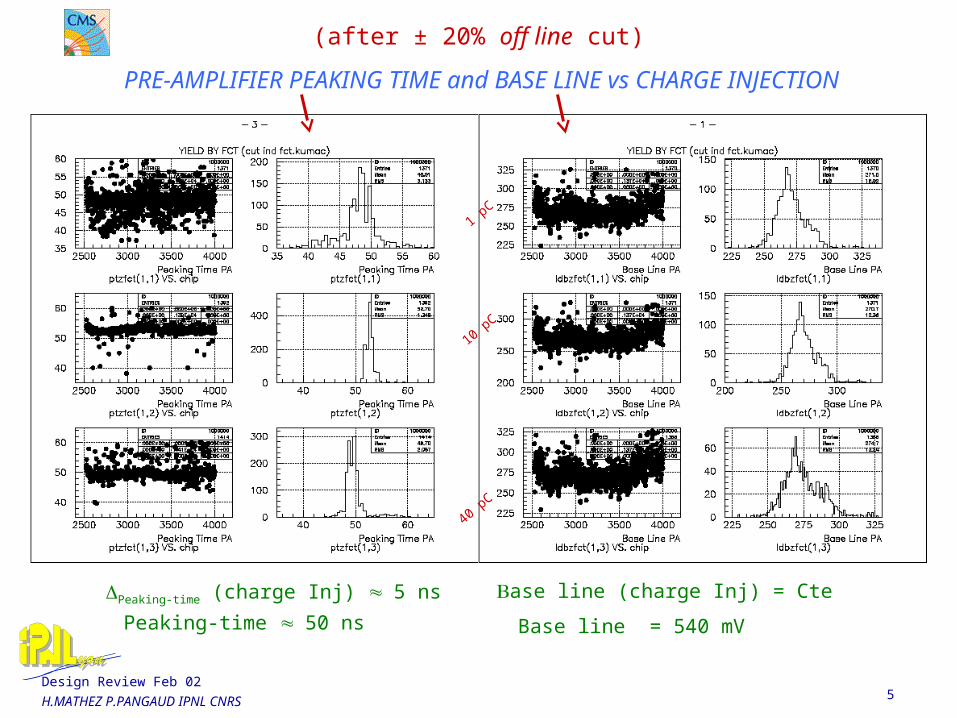
1 pC
10 pC
40 pC
(after ± 20% off line cut)
Peaking-time (charge Inj) 5 ns ase line (charge Inj) = Cte
PRE-AMPLIFIER PEAKING TIME and BASE LINE vs CHARGE INJECTION
Base line = 540 mV Peaking-time 50 ns

6
Design Review Feb 02
H.MATHEZ P.PANGAUD IPNL CNRS
(after ± 20% off line cut)
0.504 pC
1.4 pC
2 pC
1.4 pC
4 pC
6.3 pC
GAIN-AMPLIFIER (X33,X9) PEAKING TIME vs CHARGE INJECTION(in force MODE)
7
Design Review Feb 02
H.MATHEZ P.PANGAUD IPNL CNRS
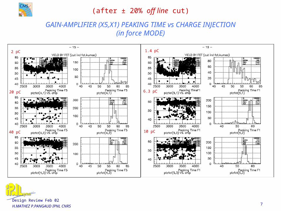
(after ± 20% off line cut)
1.4 pC
6.3 pC
10 pC
2 pC
20 pC
40 pC
GAIN-AMPLIFIER (X5,X1) PEAKING TIME vs CHARGE INJECTION(in force MODE)

8
Design Review Feb 02
H.MATHEZ P.PANGAUD IPNL CNRS
(after ± 20% off line cut)SLOW-CONTROL PART
This part measures the APD's Leakage Current (over a range of 20nA to 20µA) and the temperature of crystal plus APD (over a range of 5°C to 25°C which corresponds to a current in the thermistor of 4.3µA to 12µA).
Over the full range, the both output are between 1.9V and 2.9V which is compatiblewith the ADC input.
Temperature Measurement Leakage Current Measurement

9
Design Review Feb 02
H.MATHEZ P.PANGAUD IPNL CNRS
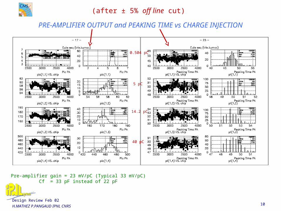
(after ± 5% off line cut)
To sort out the chips, we made some cuts at the level of ±5% on the same parameters as before.
10
Design Review Feb 02
H.MATHEZ P.PANGAUD IPNL CNRS
(after ± 5% off line cut)
Pre-amplifier gain = 23 mV/pC (Typical 33 mV/pC)Cf = 33 pF instead of 22 pF
PRE-AMPLIFIER OUTPUT and PEAKING TIME vs CHARGE INJECTION
0.504 pC
5 pC
14.2 pC
40 pC
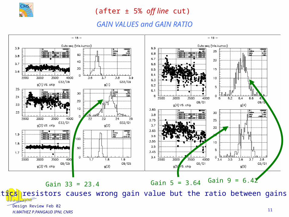
11
Design Review Feb 02
H.MATHEZ P.PANGAUD IPNL CNRS
GAIN VALUES and GAIN RATIO
Gain 9 = 6.42 Gain 5 = 3.64 Gain 33 = 23.4
(after ± 5% off line cut)
Parasitics resistors causes wrong gain value but the ratio between gains are correct.

12
Design Review Feb 02
H.MATHEZ P.PANGAUD IPNL CNRS
SLOW CONTROL NON LINEARITY OVER THE FULL RANGE
(after ± 5% off line cut)
APD's Leakage current linearity
Temperature measurement linearity
The both peak in histogram are correlatedto the change of test board.


