1 1. DISPLAY ALIGNMENT .................................................................................. 2 A. TIMING & DISPLAY SIZE ................................................................................................................ 2 B. PICTURE POSITION ....................................................................................................................... 2 C. LINEARITY ..................................................................................................................................... 2 D. ALIGNMENT PROCEDURE ............................................................................................................. 2 E. GEOMETRIC DISTORTION............................................................................................................. 3 F. WHITE BALANCE ALIGNMENT ....................................................................................................... 4 2. CONTROL AND CONNECT LAYOUT .......................................................... 7 A. MAIN PCB ...................................................................................................................................... 8 C. PIN ASSIGNMENT......................................................................................................................... 10 3. INTRODUCTION: ......................................................................................... 11 A. POWER SUPPLY ........................................................................................................................... 11 B. DEFLECTION: ............................................................................................................................... 11 C. VIDEO: .......................................................................................................................................... 11 D. DIGITAL CONTROLLOR: ............................................................................................................... 11 4. POWER SUPPLY ......................................................................................... 12 A. RECTIFIER AND FILTER CKT: ........................................................................................................ 15 B. FLYBACK AND PWM CKT : ............................................................................................................ 15 C. SNUBBER CKT: ............................................................................................................................. 15 D. SYNCHRONIZED CKT: .................................................................................................................. 15 E. POWER SAVING CKT: ................................................................................................................... 15 F. DEGAUSS CKT: ............................................................................................................................. 16 G. OVERLOAD PROTECTION CKT: .................................................................................................... 16 5. DEFLECTION ............................................................................................... 14 A. SYNC RPOCESSOR: ..................................................................................................................... 17 B. HORIZONTAL PROCESSOR .......................................................................................................... 17 C. VERTICAL OUTPUT ...................................................................................................................... 17 D. HORIZONTAL OUTPUT STAGE ..................................................................................................... 17 E. FLYBLACK TRANSFORMER.......................................................................................................... 17 6. VIDEO AMP. CIRCUIT ................................................................................. 17 A. VIDEO PRE. AMP. .......................................................................................................................... 20 B. VIDEO AMPLIFIER......................................................................................................................... 20 7. TROUBLESHOOTING ................................................................................. 19 A. POWER SUPPLY CHECK .............................................................................................................. 22 B. MONITOR CHECK FLOW CHART .................................................................................................. 23 APPENDIX A: PART LIST ............................................................................. 23 APPENDIX B: P. C. B. ASSEMBLY .............................................................. 73 APPENDIX C: DISPLAY UNIT ASSEMBLY ............................................... 108 APPENDIX D: CRT & YOKE ASSEMBLY .................................................. 122
Transcript
1
1. DISPLAY ALIGNMENT .................................................................................. 2 A. TIMING & DISPLAY SIZE ................................................................................................................ 2 B. PICTURE POSITION ....................................................................................................................... 2 C. LINEARITY ..................................................................................................................................... 2 D. ALIGNMENT PROCEDURE ............................................................................................................. 2 E. GEOMETRIC DISTORTION............................................................................................................. 3 F. WHITE BALANCE ALIGNMENT ....................................................................................................... 4
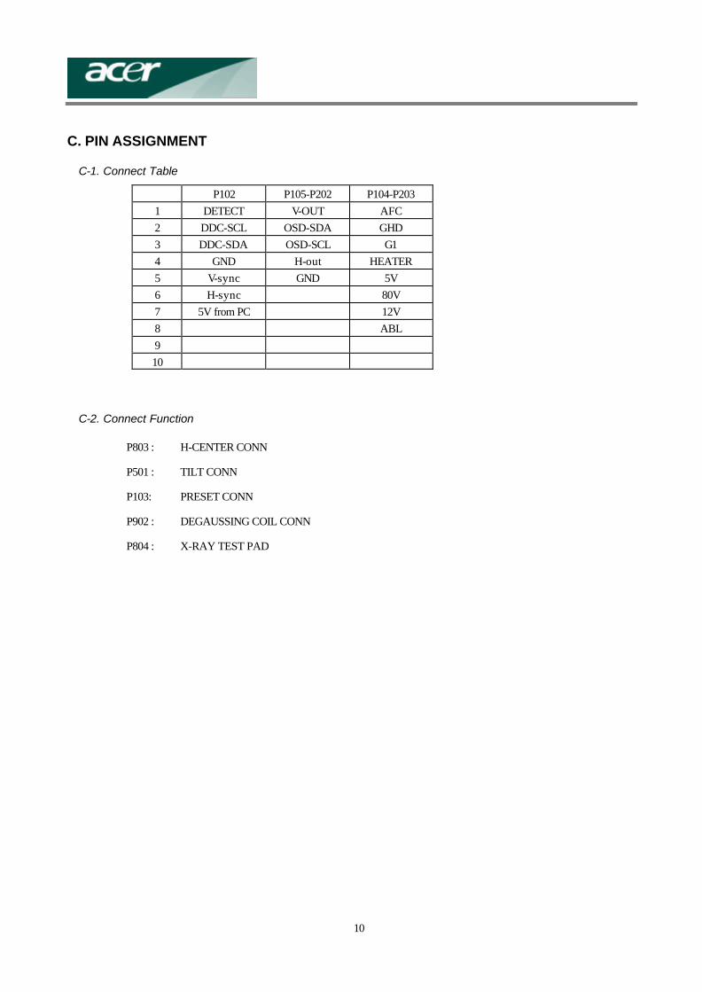
2. CONTROL AND CONNECT LAYOUT .......................................................... 7 A. MAIN PCB ...................................................................................................................................... 8 C. PIN ASSIGNMENT.........................................................................................................................10
3. INTRODUCTION: ......................................................................................... 11 A. POWER SUPPLY...........................................................................................................................11 B. DEFLECTION: ...............................................................................................................................11 C. VIDEO: ..........................................................................................................................................11 D. DIGITAL CONTROLLOR: ...............................................................................................................11
4. POWER SUPPLY .........................................................................................12 A. RECTIFIER AND FILTER CKT: ........................................................................................................15 B. FLYBACK AND PWM CKT : ............................................................................................................15 C. SNUBBER CKT: .............................................................................................................................15 D. SYNCHRONIZED CKT: ..................................................................................................................15 E. POWER SAVING CKT: ...................................................................................................................15 F. DEGAUSS CKT: .............................................................................................................................16 G. OVERLOAD PROTECTION CKT: ....................................................................................................16
5. DEFLECTION...............................................................................................14 A. SYNC RPOCESSOR: .....................................................................................................................17 B. HORIZONTAL PROCESSOR..........................................................................................................17 C. VERTICAL OUTPUT ......................................................................................................................17 D. HORIZONTAL OUTPUT STAGE .....................................................................................................17 E. FLYBLACK TRANSFORMER..........................................................................................................17
6. VIDEO AMP. CIRCUIT .................................................................................17 A. VIDEO PRE. AMP. ..........................................................................................................................20 B. VIDEO AMPLIFIER.........................................................................................................................20
7. TROUBLESHOOTING.................................................................................19 A. POWER SUPPLY CHECK ..............................................................................................................22 B. MONITOR CHECK FLOW CHART..................................................................................................23
APPENDIX A: PART LIST .............................................................................23 APPENDIX B: P. C. B. ASSEMBLY ..............................................................73 APPENDIX C: DISPLAY UNIT ASSEMBLY ...............................................108 APPENDIX D: CRT & YOKE ASSEMBLY ..................................................122
2
1. DISPLAY ALIGNMENT
A. TIMING & DISPLAY SIZE For all presetting mode shall be within the limitation: H. WIDTH 310 ± 5mm V. HEIGHT 232 ± 3 mm
The external control range of the data area, shall be as follows; Max. horizontal size : full the screen Max. vertical size : full the screen
B. PICTURE POSITION For all presetting mode shall be within the limitation: H.PHASE SCREEN CENTER ± 4 mm
V.CENTER SCREEN CENTER ± 3 mm
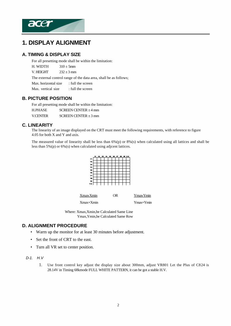
C. LINEARITY The linearity of an image displayed on the CRT must meet the following requirements, with reference to figure 4.05 for both X and Y and axis.
The measured value of linearity shall be less than 6%(p) or 8%(s) when calculated using all lattices and shall be less than 5%(p) or 6%(s) when calculated using adjcent lattices.
Xmax-Xmin OR Ymax-Ymin
Xmax+Xmin Ymax+Ymin
Where: Xmax,Xmin,be Calculated Same Line Ymax,Ymin,be Calculated Same Row
D. ALIGNMENT PROCEDURE • Warm up the monitor for at least 30 minutes before adjustment.
• Set the front of CRT to the east.
• Turn all VR set to center position.
D-1. H.V
1. Use front control key adjust the display size about 300mm, adjust VR801 Let the Plus of C824 is 28.14V in Timing 68kmode FULL WHITE PATTERN, it can be got a stable H.V.
3
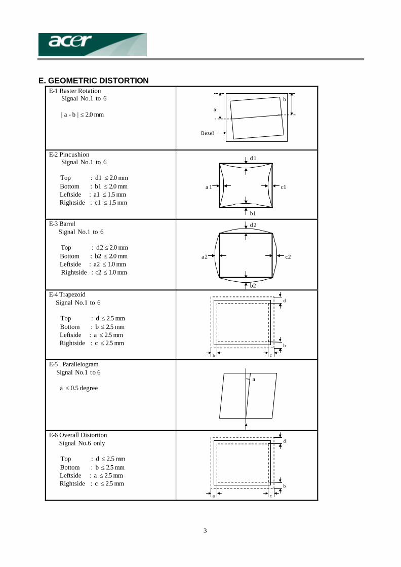
E. GEOMETRIC DISTORTION E-1 Raster Rotation Signal No.1 to 6 | a - b | ≤ 2.0 mm
a
b
Bezel
E-2 Pincushion Signal No.1 to 6 Top : d1 ≤ 2.0 mm Bottom : b1 ≤ 2.0 mm Leftside : a1 ≤ 1.5 mm Rightside : c1 ≤ 1.5 mm
a 1
b1
c1
d1
E-3 Barrel Signal No.1 to 6 Top : d2 ≤ 2.0 mm Bottom : b2 ≤ 2.0 mm Leftside : a2 ≤ 1.0 mm Rightside : c2 ≤ 1.0 mm
a2
b2
c2
d2
E-4 Trapezoid Signal No.1 to 6 Top : d ≤ 2.5 mm Bottom : b ≤ 2.5 mm Leftside : a ≤ 2.5 mm Rightside : c ≤ 2.5 mm
c
b
a
d
E-5 . Parallelogram Signal No.1 to 6 a ≤ 0.5 degree
a
E-6 Overall Distortion Signal No.6 only Top : d ≤ 2.5 mm Bottom : b ≤ 2.5 mm Leftside : a ≤ 2.5 mm Rightside : c ≤ 2.5 mm
c
b
a
d
4
F. WHITE BALANCE ALIGNMENT
F.1.1 Select timing #6 (VESA 68K 1024X768) with crosshatch pattern, adjust both horizontal and vertical OSD’s size control to get display size within 310x232p±2mm.
F.1.2 Disconnect R.G.B. signal inputs, adjust OSD’s brightness and G1 control to it’s maximum position.
F.1.3 Auto alignment(P103 must be short) Use automatic alignment equipment and program to get color temperature within specified coordinates.
F.1.4 Manual alignment P103 must be short in order to into factory mode. Select OSD function to color temperature adjustment.
F.1.5 For 9300( 7500 ; 6500 ) color coordinate ( notes: set the minimum value of R.G.B. bias is 0, set the value of sub-contrast “SC” is 0 ).
F.1.6 Disable the video pattern( for a raster pattern ), set the maximum value of contrast and brightness is 255, adjust G1 to Y=0.01 cd/mm
F.1.7 Adjust bias G to get Y=1.8 ± 0.06 cd/mm Adjust bias B to get y=297 ( y=315 for 7500 ; y=329 for 6500 ) ± 5 Adjust bias R to get x=283 ( x=295 for 7500 ; x=313 for 6500 ) ± 3
F.1.8 Fine tune the bias G and R for x=283 , y=297 ( x=299, y=315 for 7500; x=313, y=329 for 6500 ) ± 3.
F.1.9 Select 7500 and 6500 color coordinate separately. Repeat item 2.5.5 ~ 2.5.8 to meet specificity.
F.1.10 Adjust brightness control to get raster is <= 0.25cd/mm, change pattern to 2 inch square.
F.1.11 Enable G signal output of pattern generator, adjust gain G to get Y=98 ± 1 cd/mm
F.1.12 Enable B signal output, adjust gain B to get y=297 ( y=315 for 7500 ; y=329 for 6500 ) ± 2
Enable B signal output, adjust gain R to get x=283 ( x=299 for 7500 ; x=313 for 6500 ) ± 1
5
F.1.13 Fine tune the gain G and R for x=283 , y=297 ( x=299, y=315 for 7500; x=313, y=329, for 6500 ) ± 2
F.1.14 Check 150 >Y> 130 cd/mm, if not , adjust G to get Y>130 cd/mm, then repeat item 2.5.12
F.1.15 Change pattern to fall white, adjust SB to get 92< Y <113 cd/mm .
F.1.16 Select 7500 and 6500 color coordinate separately. Repeat item 2.5.11 ~ 2.5.15 to meet specificity.
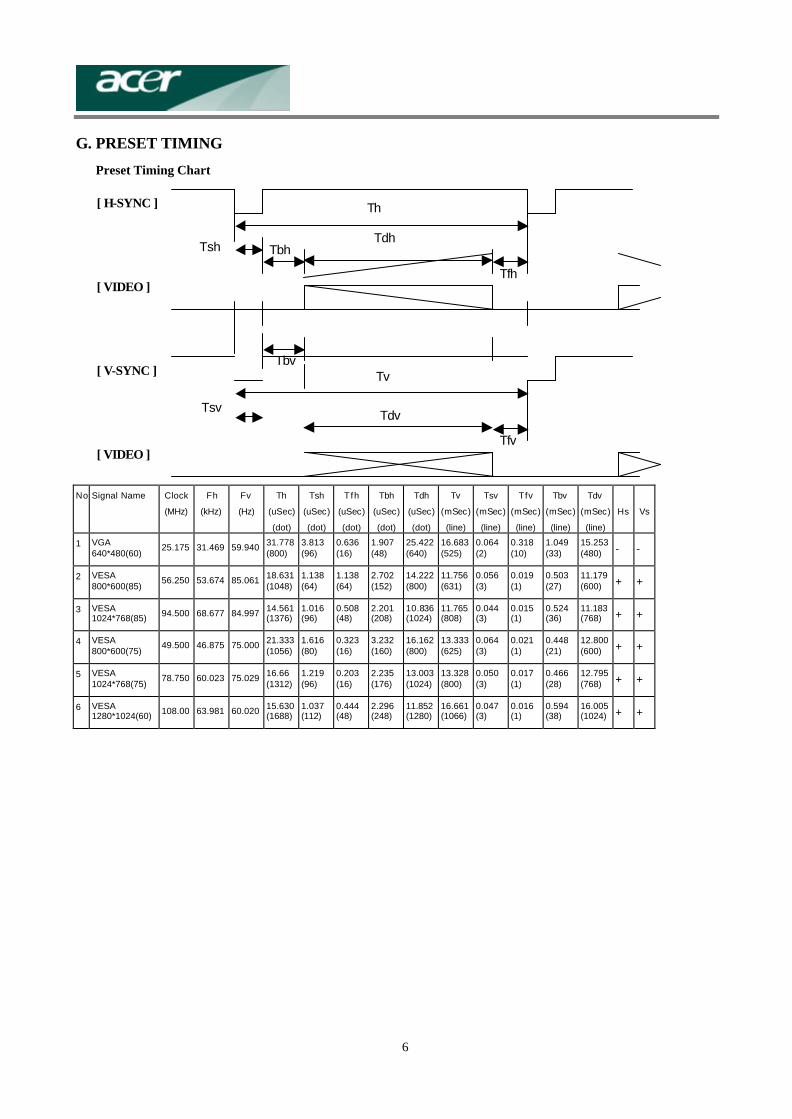
3. INTRODUCTION: C708 is a 17” multisync color monitor. The horizontal frequency range is from 30khz to 70khz, and the refresh rate is from 50hz to 160hz. The circuit includes four major parts, the power supply circuit, the deflection circuit, the video circuit and the digital control circuit. is the function block diagram.
A. POWER SUPPLY Transfer AC source to DC source that supply all the circuit power. It includes:
(1) +13.5V: For horizontal and vertical deflection circuit.
(2) –11.5V: For vertical deflection circuit.
(3) +7.2V: For CRT heater, parts of video pre-amp circuit.
(4) +53V: For B+ Boost circuit.
(5) +80V: For video circuit
(6) 9.2V: for MIRCO- P
Fig 2 is the function block diagram of power CKT.
B. DEFLECTION: Produce YOKE deflection current of horizontal and vertical, CRT H.V and bias that makes screen raster.
C. VIDEO: amplify the video signal and add the signal to the cathode of CRT to produce video on the screen.
D. DIGITAL CONTROLLOR: With the EEPROM and PROGRAM, the micro-processor (u-P) control all the picture performance.
From the key control, the user can change the H-size, V-size, V-center, H-phase.
12
R
B
G
5V
5V
5V
12V
12V
80V
13.5V
12V
12V -12V
V-scan to DY
53V
Heater 6.3V
H.V. 25KV to CRT Dynamic Focus to CRT G2 Voltage 550V to CRT
-145V
13.3V
B++16V
B
+-16V
B++16V
B
+-16V
D/A Output from uP
LM
1269 V
ideo Pre-AM
P
UP
WT
62P1
NT6827
O
SD generator
OSD DATA
EE-P-R
OM
24C08
Power
generator
-12V
9.2V
53V
80V
13.5V
78R05
78R12
LM
2467 V
ideo Output A
MP.
CR
T &
DY
ASSY
.
R,G
,B out
TD
A4856
H.V
Sync Processor
TD
A8172
Vertical O
utput AM
P.
V-sawtooth
B+
generator
H-D
river &
H-Scan Stage
FBT
H.V
generator
H-center
AD
J. G
1 AD
J. V
oltage generator
13
Fig1
1
14
Fig2
15
4. POWER SUPPLY
A. RECTIFIER AND FILTER CKT: The 90Vac-265Vac input line voltage is rectified by BD901, and smoothed by C906 to provide DC operating voltage for the circuit.
B. FLYBACK AND PWM CKT : When power is initially applied to the circuit,C909 charges through R903, Q902.When the voltage across C909 reaches a level of 16V, U901 is enabled, turning on Q903 and turning off Q902 to complete start-up action.
During the On-time of Q901, energy is stored in T900. At this time the polarity of the output windings is such that all output rectifiers are reverse biased and no energy is transferred. Primary current is sensed by R907 and compared to a DC level that is determined by voltage feedback. When this level is reached, Q901 is turned off and the polarity of all T900 windings reverses , forward biasing the output rectifiers. All the energy stored is now transferred to the output capacitors. Many cycles of this store/release action are needed to charge the outputs to their respective voltages.
The voltage across C946 is fed through a voltage divider,R970, R971, R973, C975, R976, R977 and VR901 to the error amplifier U904 compared to an internal 2.5V reference, then determine the feed back level of U901 pin 1.
C. SNUBBER CKT: Energy stored in the leakage inductance of T900 cause a voltage spike which be added to the normal reset voltage across T900 when Q901 turn off. The clamp consisting of D905, R904 and C907 limits this voltage excursion from exceeding the Vds rating of Q901.
D. SYNCHRONIZED CKT: The oscillator frequency is defined by R919, C916. The equation is approximately: Fosc=1.8/ (R919*C916). The external signal “SYN+ & SYN−”
E. POWER SAVING CKT: The monitor has ON and OFF states. The monitor enters OFF mode if H-sync and/or V-sync are removed. When in the OFF State, PS1 should below simultaneously to turn off +13.5Vs outputs. PS2 should enter PWM Pulse to pre- CRT- heater. In this state, input power should be less than 5W and LED-1 LED illuminate yellow.
16
F. DEGAUSS CKT: The DEGUSS signal which comes from micro-p to control degauss coil act or not.
When DEGUSS is high, Q950 will be saturated to make RL901 working, AC line provides a degaussing current to degauss coil.
G. OVERLOAD PROTECTION CKT: The primary current flows through the current sensing resistor R907.
The sensing voltage through the R907, R911, C914 to U901 pin3, If the current up, the U901 pin 3 voltage will be follow up, When the voltage>1 V, the U901 duty-cycle shall be limited, Made the output voltage down in the meanwhile make the U901 VCC voltage down, the U901 pin 7 fall down under 10 voltage in the then, U901 stop action, made over load for protection.
17
5. DEFLECTION
A. SYNC RPOCESSOR: H-sync & V-sync input to U1(up), then up output the H-out, V-out signal to U401 TDA4856. The H-out, V-out always are positive.
B. HORIZONTAL PROCESSOR Fig 3 is the block diagram of IC TDA4856.
The IC TDA4856 output vertical sawtooth and H-Drive signal to produce, H.V deflection. Meanwhile TDA4856 output. BDRV signal (IC pin 6) that can control B+ voltage.
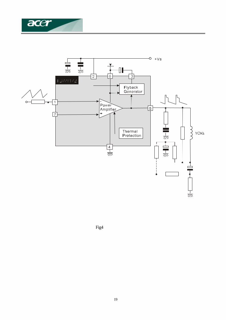
C. VERTICAL OUTPUT Fig 4 is the block diagram of IC TDA8172.
Input vertical sawtooth signal from TDA4856 to TDA8172, then TDA8172 produce vertical deflection current.
E. FLYBLACK TRANSFORMER In the primary of F.B.T, there is about 1000Vpp in the LC resonant interval, It convert to the secondary of F.B.T to produce about 25.3KV for CRT anode voltage.
18
Fig3
19
Fig4
20
Fig5
6. VIDEO AMP. CIRCUIT
A. VIDEO PRE. AMP. The video pre-amp IC is U201(LM1269). The input signal is 0.7Vpp, then pre-amp IC U201 amplify the video signal to 3~4Vpp. The U201 is controlled by up via I2C bus, Fig5 is the block diagram.
B. VIDEO AMPLIFIER The video amplifier is U203(LM2467), it amplify video signal to about 40Vpp. Video output signal add to cathode by AC coupling, Fig6 is the block diagram.. The DC bias is controlled by the IC U204(LM2480), Fig7 is the block diagram..
Fig 6 is the block diagram
21
Fig6
Fig7
22
7. TROUBLESHOOTING
A. POWER SUPPLY CHECK
23
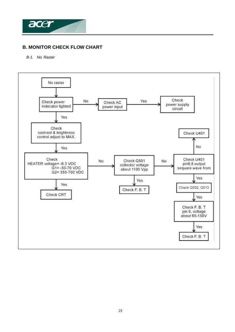
B. MONITOR CHECK FLOW CHART
B-1. No Raster
24
B-2. No Picture
25
B-3. No Vertical Deflection ( rester become a horizontal line)