1 FPGA Introduction FPGA Introduction FPGA Introduction FPGA Introduction An FPGA is an digital integrated circuit 015 An FPGA is programmable in the in the field (=outside the factory), hence the name “field programmable” ◦ Design is specified by schematics or with a hardware description o XXX ciclo 20 ◦ Design is specified by schematics or with a hardware description language ◦ Tools compute a programming file for the FPGA ◦ The FPGA is configured with the design Dottorato ◦ The FPGA is configured with the design ◦ Your electronic circuit is ready to use With an FPGA you can build electronic circuits … e dati: FPGA ◦ … without using a soldering iron ◦ … without plugging together existing modules ◦ … without having a chip pr oduced at a factor y a e acquisizion … without having a chip produced at a factory A lot of material taken from H.Sakulin lecture Elettronica
Transcript
1
FPGA IntroductionFPGA IntroductionFPGA IntroductionFPGA Introduction An FPGA is an digital integrated circuit
015
g g An FPGA is programmable in the in the field (=outside the
factory), hence the name “field programmable”◦ Design is specified by schematics or with a hardware description
oX
XX
cic
lo20 ◦ Design is specified by schematics or with a hardware description
language◦ Tools compute a programming file for the FPGA◦ The FPGA is configured with the design
Dot
tora
to ◦ The FPGA is configured with the design◦ Your electronic circuit is ready to use
With an FPGA you can build electronic circuits …
eda
ti: F
PGA ◦ … without using a soldering iron
◦ … without plugging together existing modules◦ … without having a chip produced at a factory
ae
acqu
isiz
ion … without having a chip produced at a factory
A lot of material taken from H.Sakulin lecture
Elet
tron
ica
2
What’s inside an FPGAWhat’s inside an FPGAWhat s inside an FPGAWhat s inside an FPGA01
5o
XX
X c
iclo
20D
otto
rato
eda
ti: F
PGA
ae
acqu
isiz
ion
Elet
tron
ica
3
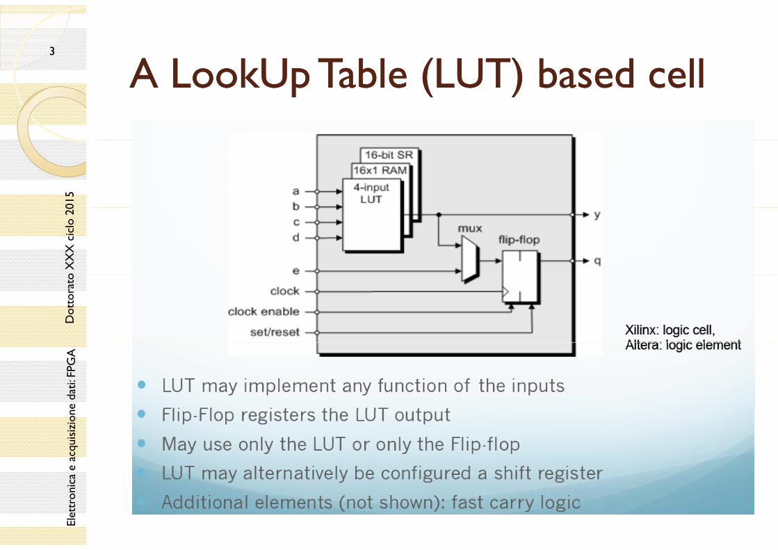
A A LookUpLookUp Table (LUT) based cellTable (LUT) based cellA A LookUpLookUp Table (LUT) based cellTable (LUT) based cell01
Schematic◦ Graphical overview◦ Can draw entire design
oX
XX
cic
lo20 ◦ Use pre-defined blocks
HDL: Verilog, VHDLC bl k l
Dot
tora
to ◦ Can generate blocks using loops◦ Can synthesize algorithms◦ (Almost) independent of design tool
eda
ti: F
PGA
◦ (Almost) independent of design tool◦ May use tools used in SW development (CVS, SVN …)
New trends
ae
acqu
isiz
ion
◦ C-like languages (handle-C, system-C, …)◦ Labview
Elet
tron
ica
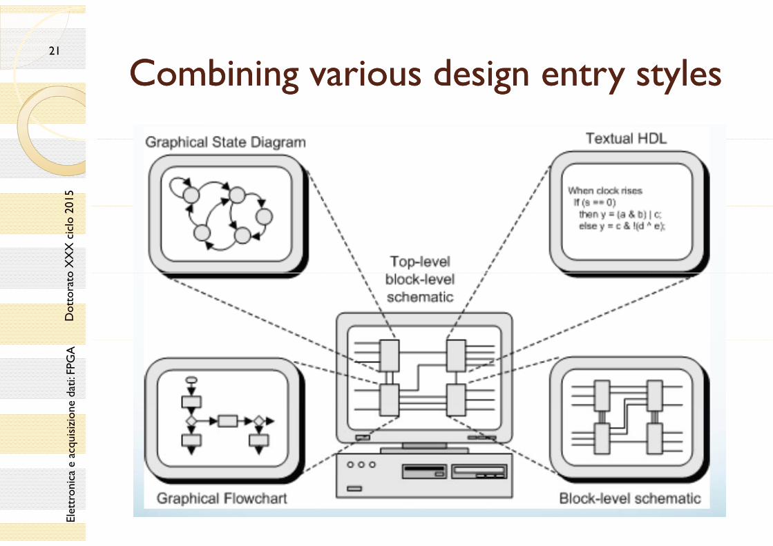
Schematic and HDL are often combined together
21
Combining various design entry stylesCombining various design entry stylesCombining various design entry stylesCombining various design entry styles01
5o
XX
X c
iclo
20D
otto
rato
eda
ti: F
PGA
ae
acqu
isiz
ion
Elet
tron
ica
22
Design FlowDesign FlowDesign FlowDesign Flow01
5o
XX
X c
iclo
20D
otto
rato
eda
ti: F
PGA
ae
acqu
isiz
ion
Elet
tron
ica
23
First Level Trigger at collidersFirst Level Trigger at collidersFirst Level Trigger at collidersFirst Level Trigger at colliders01
5o
XX
X c
iclo
20D
otto
rato
eda
ti: F
PGA
ae
acqu
isiz
ion
Elet
tron
ica
24
FPGA used in trigger logic because:FPGA used in trigger logic because:FPGA used in trigger logic because:FPGA used in trigger logic because: They are fast
015
They are fast◦ Much faster than discrete electronics (shorter
connections)
oX
XX
cic
lo20
Many parallel inputs◦ Data from many parts of the detector has to be
b d
Dot
tora
to combined◦ Can send parallel data rather than serialAll ti f d i ll l
eda
ti: F
PGA All operations are performed in parallel
◦ Can build pipelined logic They can be re programmed
ae
acqu
isiz
ion They can be re-programmed◦ Trigger algorithms can be optimized
Elet
tron
ica
25
FPGA used in data acquisitionFPGA used in data acquisitionFPGA used in data acquisitionFPGA used in data acquisition Frontend Electronics
015
Frontend Electronics◦ Pedestal subtraction◦ Zero suppression
oX
XX
cic
lo20 ◦ Compression
◦ …C d li k
Dot
tora
to Custom data links◦ E.g. SLINK-64 Several serial LVDS links in parallel
eda
ti: F
PGA
Several serial LVDS links in parallel Up to 400 MB/s
Interface from custom hardware to commercial l i
ae
acqu
isiz
ion electronics◦ PCI bus, VME bus, Myrinet, etc.
Elet
tron
ica
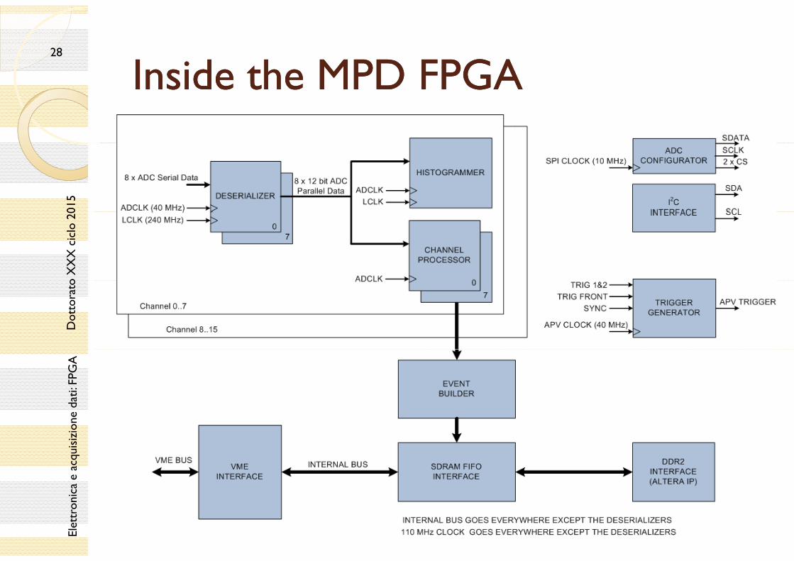
26 Example: Multi Purpose Digitizer (MPD)Example: Multi Purpose Digitizer (MPD) 16 channels, differntial, 12 bit, up to 50 MHz, synchronous ADC, Full-
Scale Range: 2Vpp 4 x HDMI-A front panel connectors for analog inputs
015
p g p 2 x HDMI-A front panel connectors for digital controls (clock, fast
commands, I2C) 2 +2 general purpose coaxial (LEMO 00) front panel inputs and outputs,
software selectable NIM or LVTTL levels
oX
XX
cic
lo20
software selectable NIM or LVTTL levels Front panel coaxial (LEMO 00) clock input, 40 MHz, LVTTL, 50
terminated 10-100 RJ-45 copper Ethernet port
SFP f l i i bi i l li k i
Dot
tora
to SFP cage for multigigabit optical link connection 4 general purpose LEDs VXS connector option, 4 RX and 4 TX pairs connected to the FPGA ADC clock phase adjustable to compensate cable delay
eda
ti: F
PGA
ADC clock phase adjustable to compensate cable delay Logic functions based on Altera ARRIA-GX EP1AGX60F780 FPGA On board real time data processing capabilities VME 64x compliant with up to 2eSST cycles
ae
acqu
isiz
ion
VME live insertion capabilities 128 MB DDR2 SDRAM SD-Card interface
S l 5V l
Elet
tron
ica
Single +5V power supply Expansion option using PMC compliant connectors VME based or standalone operation