30
1 HFT Technology and Mechanical Design Wieman RNC LBNL TAC Review Wed. 11:30 – 12:05 15-Mar-2006
| Date post: | 26-Dec-2015 |
| Category: |
Documents |
| Upload: | sharon-baldwin |
| View: | 214 times |
| Download: | 0 times |
1
HFT Technology and Mechanical Design
Wieman RNCLBNL
TAC ReviewWed. 11:30 – 12:05 15-Mar-2006
2
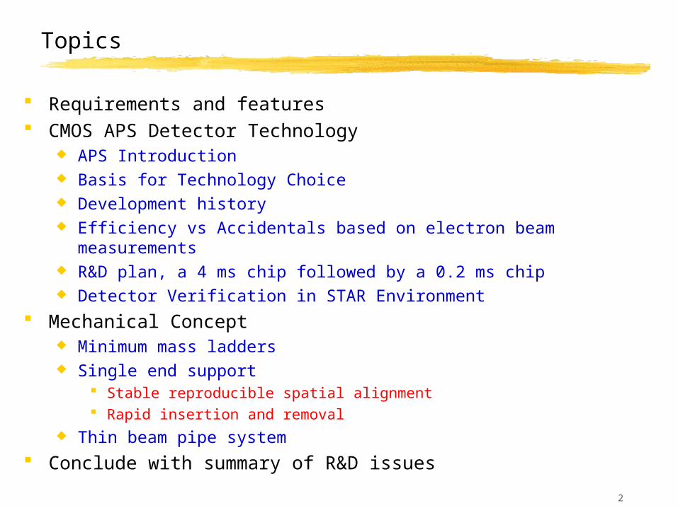
Topics
Requirements and features CMOS APS Detector Technology
APS Introduction Basis for Technology Choice Development history Efficiency vs Accidentals based on electron beam measurements R&D plan, a 4 ms chip followed by a 0.2 ms chip Detector Verification in STAR Environment
Mechanical Concept Minimum mass ladders Single end support
Stable reproducible spatial alignment Rapid insertion and removal
Thin beam pipe system Conclude with summary of R&D issues
3
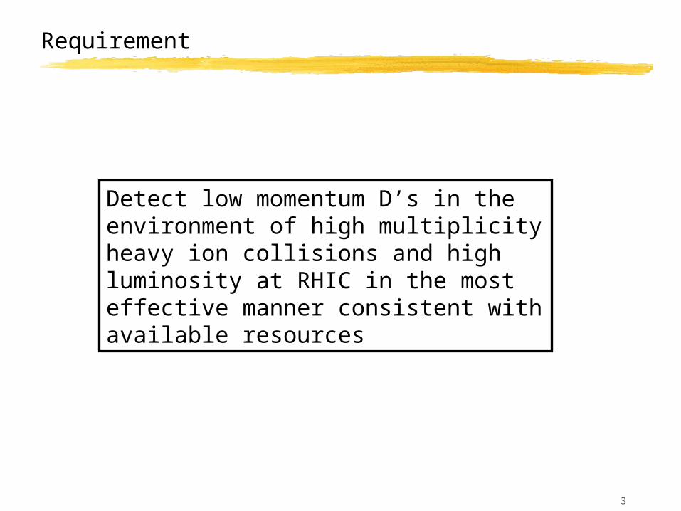
Requirement
Detect low momentum D’s in the environment of high multiplicity heavy ion collisions and high luminosity at RHIC in the most effective manner consistent with available resources
4
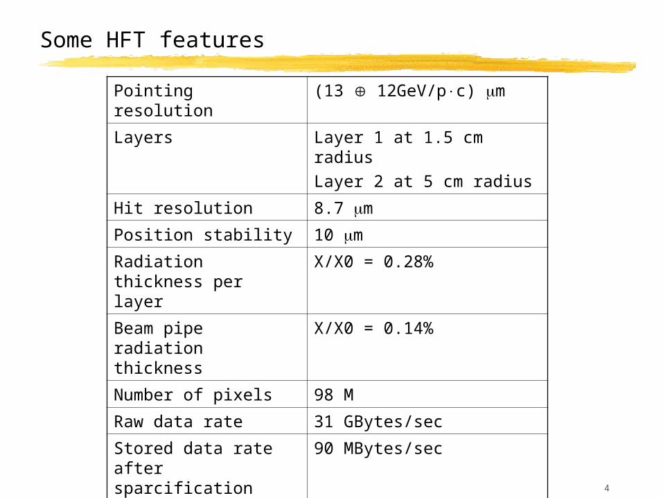
Some HFT features
Pointing resolution (13 12GeV/pc) m
Layers Layer 1 at 1.5 cm radiusLayer 2 at 5 cm radius
Hit resolution 8.7 m
Position stability 10 m
Radiation thickness per layer
X/X0 = 0.28%
Beam pipe radiation thickness
X/X0 = 0.14%
Number of pixels 98 M
Raw data rate 31 GBytes/sec
Stored data rate after sparcification
90 MBytes/sec
Integration time (affects pileup)
R&D phase 4 msFinal detector 0.2 ms
Rapid installation and replacement
Reproducible positioning
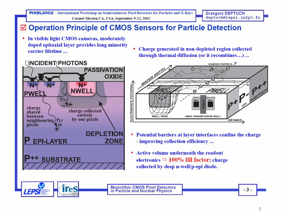
5
6
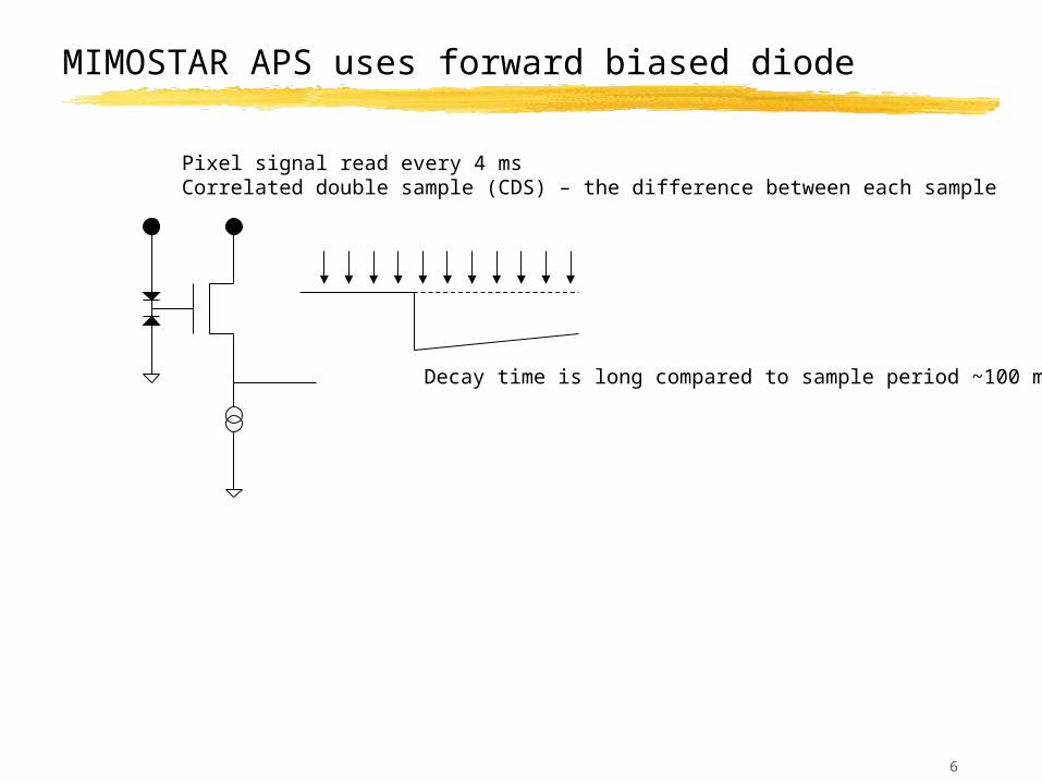
MIMOSTAR APS uses forward biased diode
Pixel signal read every 4 msCorrelated double sample (CDS) – the difference between each sample
Decay time is long compared to sample period ~100 ms
7
Basis for CMOS APS Technology Choice
Hybrid technology (silicon pixels bump bonded to ASIC readout) Advantages:
Very fast, short integration time, no pileup Potential for trigger generation Rad hard Well established technology, ATLAS etc
Disadvantages: Too thick for optimum pointing accuracy required for low momentum D
meson reconstruction Additional mass required for cooling Requires establishing complicated partnerships for production and
testing (can’t just buy units)
8
Basis for CMOS APS Technology Choice
CCD technology Advantage:
Successfully used in high precision vertex detector, VXD3 of SLD Disadvantages:
Limited radiation tolerance Sufficient readout speed pushes technology boundaries Limited industry access
DEPFET technology Advantages:
Excellent signal to noise Sophisticated thin ladder structures High speed Probably RAD hard
Disadvantages: Single foundry Highly specialized one of a kind technology No currently installed systems
9
Basis for CMOS Technology Choice
CMOS APS technology Advantages:
Relatively RAD hard Available through multiple standard CMOS foundries Inexpensive commercial thinning Good success rate making working detectors by many institutions Excellent position resolution and fine granularity Partnered with the leading institution, IReS (now IPHC) in Strasburg Young technology, can expect considerable growth in capability
Disadvantages: Young technology for vertex detectors, currently no installed systems Limited signal to noise Current designs have relatively long integration times, i.e. potential
pileup at highest luminosities
10
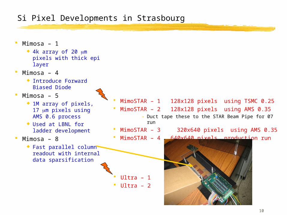
Si Pixel Developments in Strasbourg
Mimosa – 1 4k array of 20 m
pixels with thick epi layer
Mimosa – 4 Introduce Forward
Biased Diode Mimosa – 5
1M array of pixels, 17 m pixels using AMS 0.6 process
Used at LBNL for ladder development
Mimosa – 8 Fast parallel column
readout with internal data sparsification
MimoSTAR – 1 128x128 pixels using TSMC 0.25 MimoSTAR – 2 128x128 pixels using AMS 0.35
– Duct tape these to the STAR Beam Pipe for 07 run
MimoSTAR – 3 320x640 pixels using AMS 0.35 MimoSTAR – 4 640x640 pixels production run
Ultra – 1 Ultra – 2
11
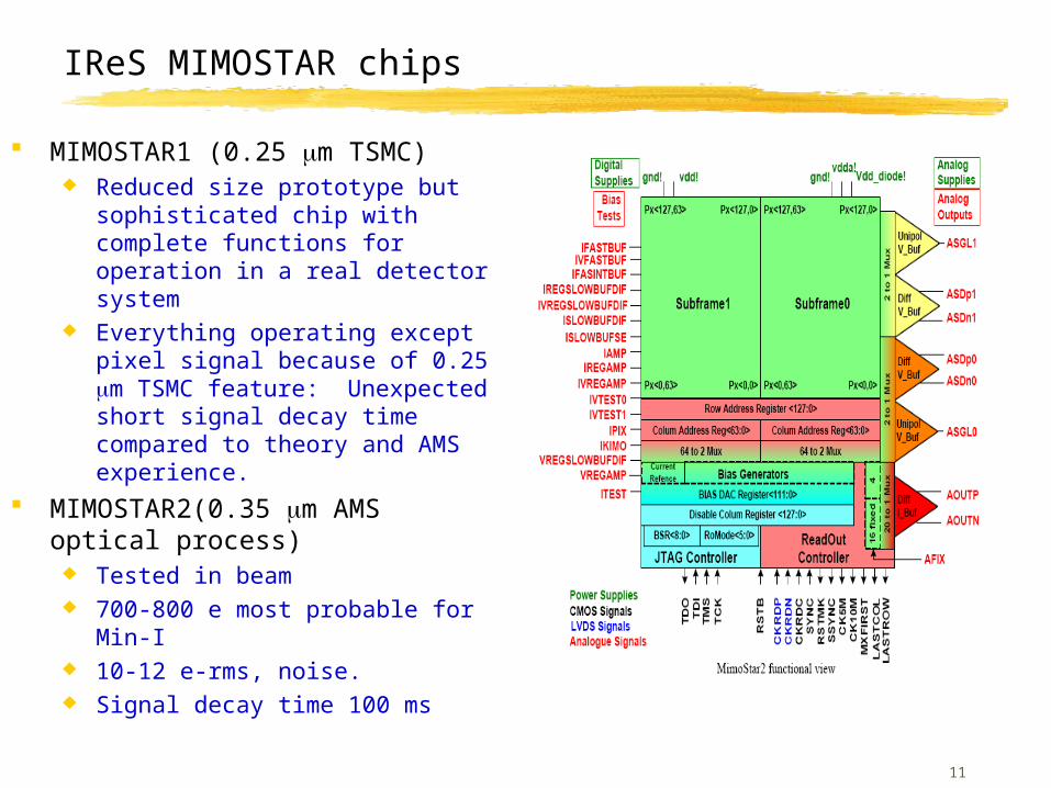
IReS MIMOSTAR chips
MIMOSTAR1 (0.25 m TSMC) Reduced size prototype but
sophisticated chip with complete functions for operation in a real detector system
Everything operating except pixel signal because of 0.25 m TSMC feature: Unexpected short signal decay time compared to theory and AMS experience.
MIMOSTAR2(0.35 m AMS optical process) Tested in beam 700-800 e most probable for Min-I 10-12 e-rms, noise. Signal decay time 100 ms
12
MIMOSTAR2, features
Parallel voltage out - for readout chip (abandoned)
Serial current loop out – for off ladder ADC up to 80 MHz
128 X 128 ½ Standard forward bias design ½ Rad Hard forward bias design, reduced
oxide Leakage Current 3-5 fA at room
temperature, shot noise adds 4 e-rms for 4 ms integration (total noise 16 e-rms)
Min-I cluster signal 700-800 e Successful radiation test, 20 Krad OK
13
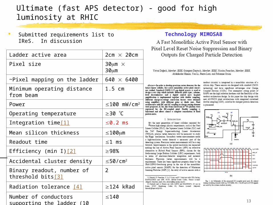
Ultimate (fast APS detector) - good for high luminosity at RHIC
Submitted requirements list to IReS. In discussion
Technology MIMOSA8
Ladder active area 2cm 20cm
Pixel size 30m 30m
~Pixel mapping on the ladder 640 6400
Minimum operating distance from beam 1.5 cm
Power 100 mW/cm2
Operating temperature 30 C
Integration time[1] 0.2 ms
Mean silicon thickness 100m
Readout time 1 ms
Efficiency (min I)[2] 98%
Accidental cluster density 50/cm2
Binary readout, number of threshold bits[3]
2
Radiation tolerance [4] 124 kRad
Number of conductors supporting the ladder (10 chips/ladder)[5]
140
Triggered readout, maximum trigger delay[6]
2 s
14
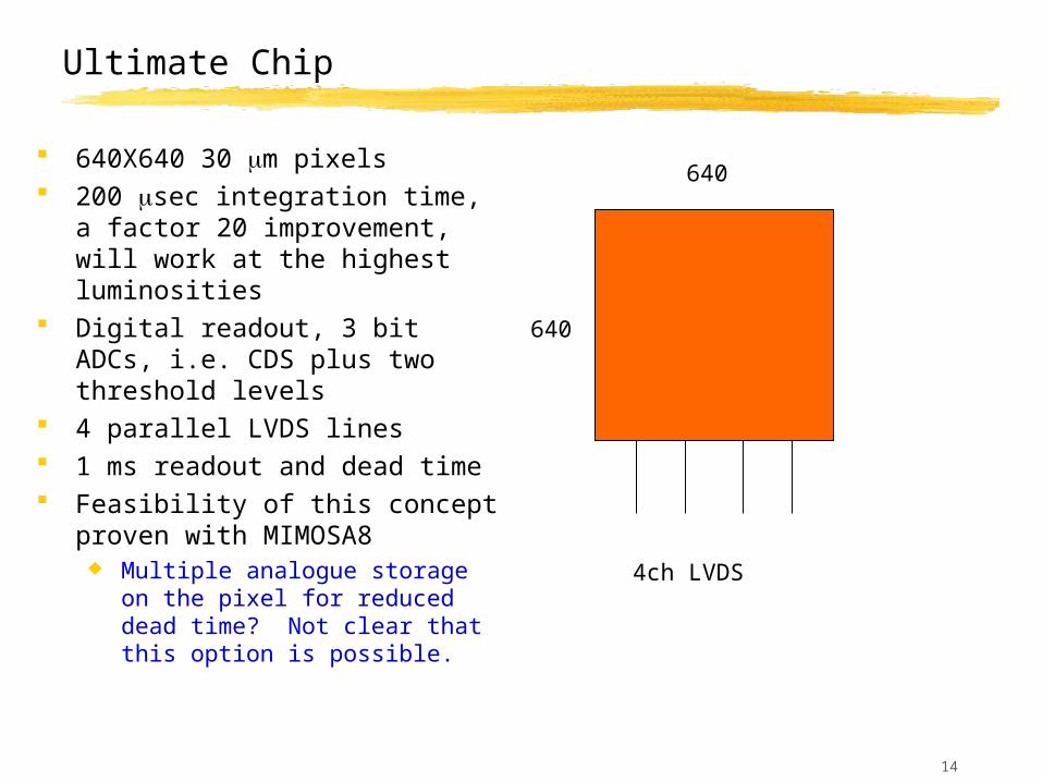
Ultimate Chip
640X640 30 m pixels 200 sec integration time, a
factor 20 improvement, will work at the highest luminosities
Digital readout, 3 bit ADCs, i.e. CDS plus two threshold levels
4 parallel LVDS lines 1 ms readout and dead time Feasibility of this concept
proven with MIMOSA8 Multiple analogue storage on
the pixel for reduced dead time? Not clear that this option is possible.
4ch LVDS
640
640
15
Efficiency vs Accidentals
A critical issue with thin APS CMOS detectors Can data sparcification be achieved without loss of efficiency? Following study shows that planned simple high speed
algorithm will work
16
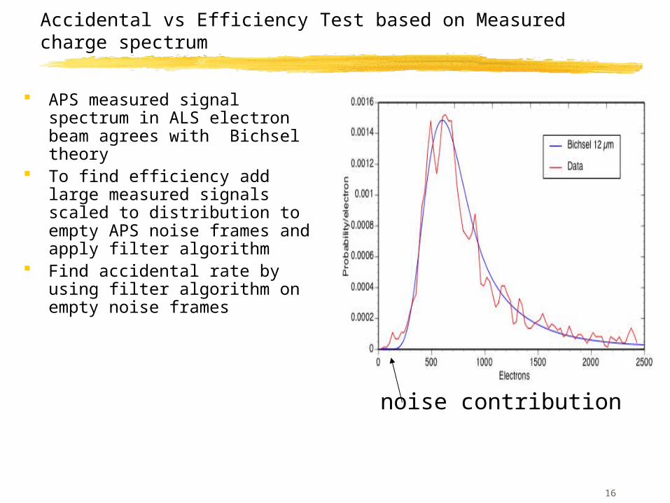
Accidental vs Efficiency Test based on Measured charge spectrum
APS measured signal spectrum in ALS electron beam agrees with Bichsel theory
To find efficiency add large measured signals scaled to distribution to empty APS noise frames and apply filter algorithm
Find accidental rate by using filter algorithm on empty noise frames
noise contribution
17
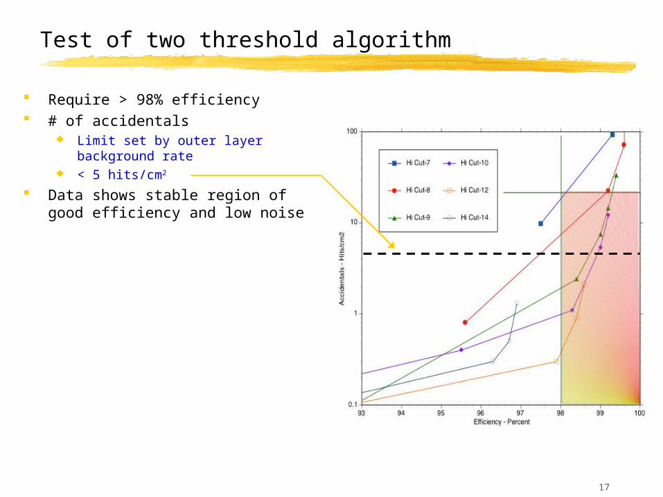
Test of two threshold algorithm
Require > 98% efficiency # of accidentals
Limit set by outer layer background rate
< 5 hits/cm2
Data shows stable region of good efficiency and low noise
18
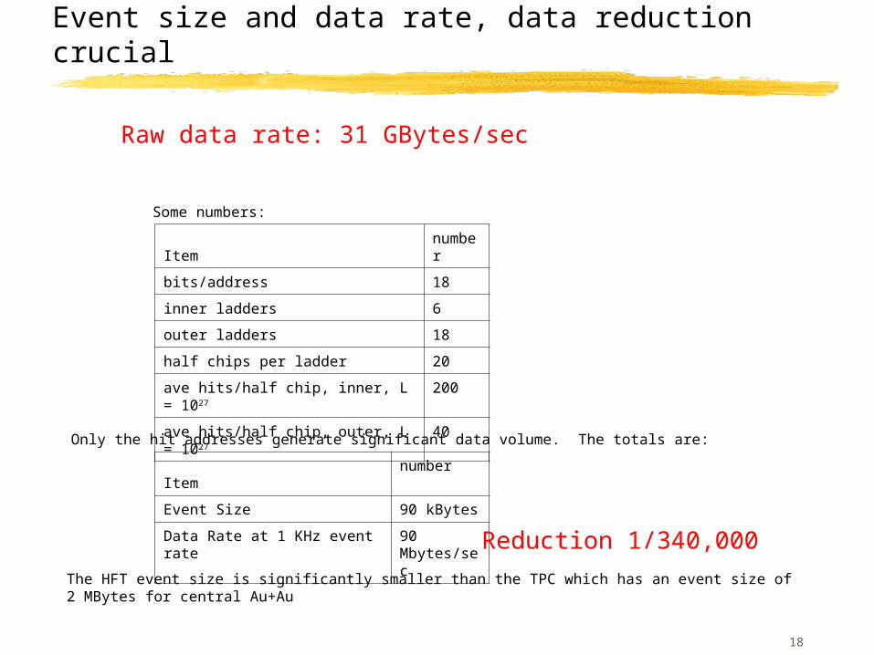
Event size and data rate, data reduction crucial
Some numbers:
Itemnumber
bits/address 18
inner ladders 6
outer ladders 18
half chips per ladder 20
ave hits/half chip, inner, L = 1027 200
ave hits/half chip, outer, L = 1027 40
Only the hit addresses generate significant data volume. The totals are:
Itemnumber
Event Size 90 kBytes
Data Rate at 1 KHz event rate 90 Mbytes/sec
The HFT event size is significantly smaller than the TPC which has an event size of 2 MBytes for central Au+Au
Raw data rate: 31 GBytes/sec
Reduction 1/340,000
19
R&D Plans, Scope change
R&D phase for technology verification using MIMOSTAR2 (4 ms integration) technology Install n 4 ladder modules Verify mechanical insertion technology and stability control Verify DAQ and data reduction technology
Final phase MIMOSTAR-Ultimate (200 s integration) Full 24 ladder, 2, installation Multiple backup copies for rapid repair The full luminosity solution
20
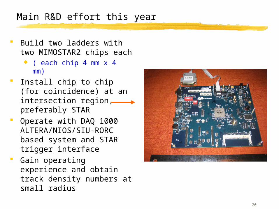
Main R&D effort this year
Build two ladders with two MIMOSTAR2 chips each ( each chip 4 mm x 4 mm)
Install chip to chip (for coincidence) at an intersection region, preferably STAR
Operate with DAQ 1000 ALTERA/NIOS/SIU-RORC based system and STAR trigger interface
Gain operating experience and obtain track density numbers at small radius
21
Mechanical
Mechanical support Beam pipe
22
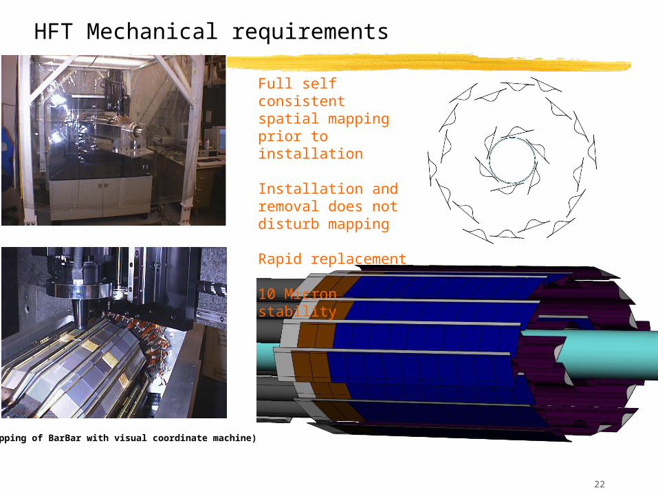
HFT Mechanical requirements
Full self consistent spatial mapping prior to installation
Installation and removal does not disturb mapping
Rapid replacement
10 Micron stability
(mapping of BarBar with visual coordinate machine)
23
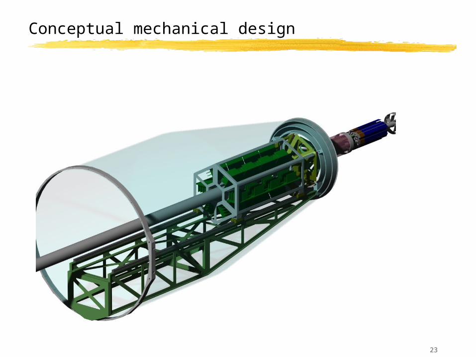
Conceptual mechanical design
24
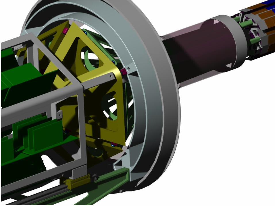
25
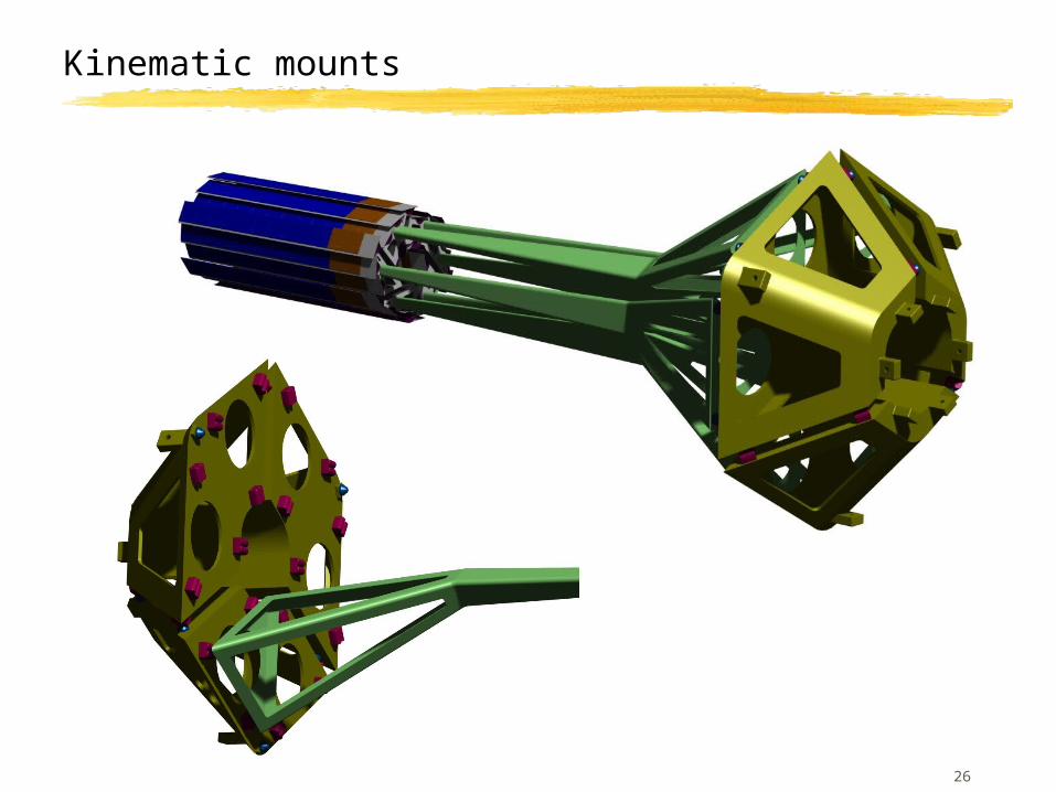
26
Kinematic mounts
27
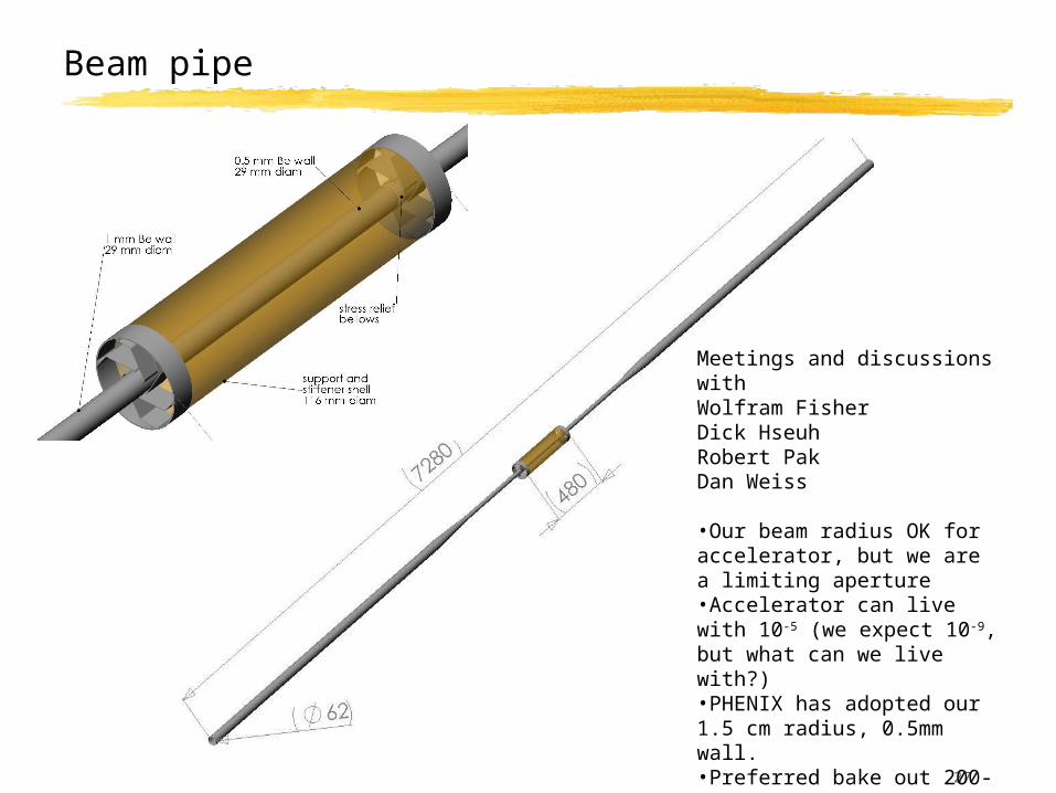
Beam pipe
Meetings and discussions with Wolfram FisherDick HseuhRobert PakDan Weiss
•Our beam radius OK for accelerator, but we are a limiting aperture•Accelerator can live with 10-5 (we expect 10-9, but what can we live with?)•PHENIX has adopted our 1.5 cm radius, 0.5mm wall.•Preferred bake out 200-250 C to activate NEG coating
28
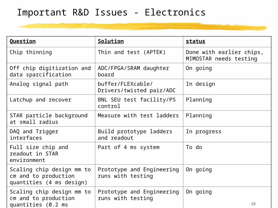
Important R&D Issues - Electronics
Question Solution status
Chip thinning Thin and test (APTEK) Done with earlier chips, MIMOSTAR needs testing
Off chip digitization and data sparcification
ADC/FPGA/SRAM daughter board
On going
Analog signal path buffer/FLEXcable/Drivers/twisted pair/ADC
In design
Latchup and recover BNL SEU test facility/PS control
Planning
STAR particle background at small radius
Measure with test ladders Planning
DAQ and Trigger interfaces Build prototype ladders and readout
In progress
Full size chip and readout in STAR environment
Part of 4 ms system To do
Scaling chip design mm to cm and to production quantities (4 ms design)
Prototype and Engineering runs with testing
On going
Scaling chip design mm to cm and to production quantities (0.2 ms design)
Prototype and Engineering runs with testing
On going
29
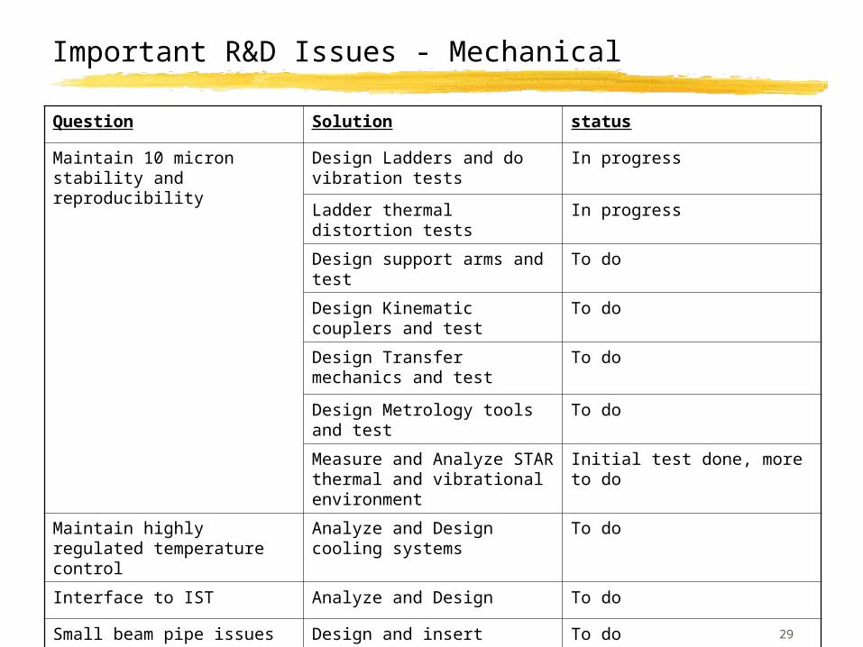
Important R&D Issues - Mechanical
Question Solution status
Maintain 10 micron stability and reproducibility
Design Ladders and do vibration tests
In progress
Ladder thermal distortion tests
In progress
Design support arms and test
To do
Design Kinematic couplers and test
To do
Design Transfer mechanics and test
To do
Design Metrology tools and test
To do
Measure and Analyze STAR thermal and vibrational environment
Initial test done, more to do
Maintain highly regulated temperature control
Analyze and Design cooling systems
To do
Interface to IST Analyze and Design To do
Small beam pipe issues Design and insert To do
30
Conclusion


