Thin-films for Thermoelectric Applications M. F. Silva, J. F. Ribeiro, J. P. Carmo, L. M. Goncalves, and J. H. Correia University of Minho - Dept. Industrial Electronics 4800-058 Azurem, Guimaraes, PORTUGAL {fsilva, jribeiro, jcarmo, lgoncalves, higino.correia}@dei.uminho.pt Abstract The introduction of nanotechnology and new horizons enabled previously unattainable by thermoelectric devices. The nano-scale phenomena began to be exploited through techniques of thin-film depositions to increase the efficiency of thermoelectric films. This chapter reviews the fundamentals of the phenomenon of thermoelectricity and its evolution since it was discovered in 1822. This chapter also makes a review about the thermoelectric devices the macro to nano devices, where it is described the most used techniques of physical vapor depositions to deposit thermoelectric thin-films. Then, it is presented a custom made deposition chamber for depositing thermoelectric thin-films by the thermal co-evaporation technique, where the construction issues and specifications are discussed. All the steps for obtaining a thermoelectric generator in flexible substrate with the custom deposition chamber (to incorporate in thermoelectric microsystem) are described. The aim of thermoelectric microsystem relays to introduce in a human energy harvesting applications to power wireless sensor networks (WSN) or biomedical devices. The scanning probe measuring systems for characterization of the thermoelectric thin-films are also described in this chapter. Finally, a few number of prototypes of thermoelectric thin-films (made of bismuth and antimony tellurides, Bi 2 Te 3 and Sb 2 Te 3 , respectively) were obtained by co-evaporation (using the custom made deposition chamber) and characterized for quality assessment. All of the issues involved in the co-evaporation and characterization are object of analysis in this chapter. Key words: Thin-films, thermoelectricity, energy harvesting. 1 Introduction The need for production of electricity by mankind has intensified and is likely to increase. Much of the actions of human beings inevitably require a power source, whether in food, transportation or work. The energy sources from fossil materials shall disappear, and therefore, the solution in generating electricity lies from renewable sources. Renewable energy solutions exist to date, and the one that brings a greater potential is the thermal/geothermal. Not always the source is available in solutions for renewable energies such as sunlight, wind or water. The increase in global temperature of the Earth produces a great potential for generating electricity by heat released or waste heat. The phenomenon of thermoelectricity may be the solution to be adopted in renewable energy thermal/geothermal applications. One of the challenges that mobile devices face is the need to obtain a reliable source of power, beyond the limitations imposed by the batteries. The solution lies in devices capable of recovering energy from the environment surrounding the device or the user. The human body radiates heat continuously and the devices that are in direct contact can recovery the waste heat, i.e., the thermoelectric generators (TEG). Until now TEGs have low efficiency, a factor that has been changing in recent years with the use of thin-film deposition techniques and the exploration of phenomena at the nano-scale. It thus becomes important to build systems capable of producing thin films for flexible microsystems for production of electricity. 1.1Thermoelectricity In 1822 Thomas Seebeck discovered that if applied a temperature gradient between the junction of two different materials, occurs an voltage like in a temperature sensor, and consequently by an electric current in a closed circuit as a thermoelectric generator (in Fig. 1) [1]. The Seebeck effect () is given by the difference of temperature (ΔT) which causes a voltage difference (ΔV). = ∆ ∆ , [μVK ] (1) Fig. 1. Seebeck experiment; (a) Temperature sensor; (b) Thermoelectric generator.
Transcript
Thin-films for Thermoelectric Applications
M. F. Silva, J. F. Ribeiro, J. P. Carmo, L. M. Goncalves, and J. H. Correia
University of Minho - Dept. Industrial Electronics 4800-058 Azurem, Guimaraes, PORTUGAL
The introduction of nanotechnology and new horizons enabled previously unattainable by thermoelectric devices. The nano-scale phenomena began to be exploited through techniques of thin-film depositions to increase the efficiency of thermoelectric films. This chapter reviews the fundamentals of the phenomenon of thermoelectricity and its evolution since it was discovered in 1822. This chapter also makes a review about the thermoelectric devices the macro to nano devices, where it is described the most used techniques of physical vapor depositions to deposit thermoelectric thin-films. Then, it is presented a custom made deposition chamber for depositing thermoelectric thin-films by the thermal co-evaporation technique, where the construction issues and specifications are discussed. All the steps for obtaining a thermoelectric generator in flexible substrate with the custom deposition chamber (to incorporate in thermoelectric microsystem) are described. The aim of thermoelectric microsystem relays to introduce in a human energy harvesting applications to power wireless sensor networks (WSN) or biomedical devices. The scanning probe measuring systems for characterization of the thermoelectric thin-films are also described in this chapter. Finally, a few number of prototypes of thermoelectric thin-films (made of bismuth and antimony tellurides, Bi2Te3 and Sb2Te3, respectively) were obtained by co-evaporation (using the custom made deposition chamber) and characterized for quality assessment. All of the issues involved in the co-evaporation and characterization are object of analysis in this chapter. Key words: Thin-films, thermoelectricity, energy harvesting.
1 Introduction The need for production of electricity by mankind has intensified and is likely to increase. Much of the actions of human beings inevitably require a power source, whether in food, transportation or work. The energy sources from fossil materials shall disappear, and therefore, the solution in generating electricity lies from renewable sources. Renewable energy solutions exist to date, and the one that brings a greater potential is the thermal/geothermal. Not always the source is available in solutions for renewable energies such as sunlight, wind or water. The increase in global temperature of the Earth produces a great potential for generating electricity by heat released or waste heat. The phenomenon of thermoelectricity may be the solution to be adopted in renewable energy thermal/geothermal applications. One of the challenges that mobile devices face is the need to obtain a reliable source of power, beyond the limitations imposed by the batteries. The solution lies in devices capable of recovering energy from the environment surrounding the device or the user. The human body radiates heat continuously and the devices that are in direct contact can recovery the waste heat, i.e., the thermoelectric generators (TEG). Until now TEGs have low efficiency, a factor that has been changing in recent years with the use of thin-film deposition techniques and the exploration of phenomena at the nano-scale. It thus becomes important to build systems capable of producing thin films for flexible microsystems for production of electricity.
1.1 Thermoelectricity In 1822 Thomas Seebeck discovered that if applied a temperature gradient between the junction of two different materials, occurs an voltage like in a temperature sensor, and consequently by an electric current in a closed circuit as a thermoelectric generator (in Fig. 1) [1]. The Seebeck effect () is given by the difference of temperature (ΔT) which causes a voltage difference (ΔV).
= ∆!∆" , [µVK%&] (1)
Fig. 1. Seebeck experiment; (a) Temperature sensor; (b) Thermoelectric generator.
Only 12 years later Jean Peltier found that in the junction of two materis – bismuth (Bi) and Antimony (Sb) – thermic energy is released or absorbed depending on the electric current [2]. Although Peltier used the Seebeck effect in his experiments, he could not estimate the foundations of their observations or relate to the effect Seebeck's findings. Only in 1838 Heinrich Lenz was able to explain the nature of the Peltier effect with an simple experiment (Fig. 2) [3,4]. He put a drop of water on top of the junction of bismuth (Bi) and antimony (Sb). He managed to freeze the water drop and changing the direction of electric current between junctions, it melted.
Thus Lenz made the first thermoelectric device. In 1851 William Thomson - better known as Lord Kelvin and the absolute temperature scale - proposed in 1848 [5] to establish the Peltier coefficient (') may be related to the Seebeck coefficient () using the following formula.
' = " , [V] (2)
Where " represents the temperature of in junction of the materials [6]. Thomson predicted the existence of a third effect. The Thomson effect defines the cooling and heating of an electrical conductor in the presence of electric current when exposed to a gradient temperature. It is generally despised for being well below the Peltier effect [7]. In 1885 John William Strutt also known as the 3rd Baron Rayleigth (Nobel Prize in physics 1904) used the phenomenon of thermoelectric power generation but with incorrect calculations and regarding the efficiency of thermoelectric generator [8]. Studies on the satisfactory thermoelectric generation and cooling were achieved by Edmund Altenkirch in 1909 and 1911 [9,10]. Altenkirch concluded that good thermoelectric materials needed to have a high Seebeck coefficient () but with low thermal conductivity (() to retain heat in the junction, and low electrical resistivity ()) to minimize the Joule heating. These properties would then be designated to characterize the thermoelectric materials by assigning the name of figure of merit (*).
* = + -( , [K%&] (3)
Where (-) represents the electrical conductivity inverse to the electrical resistivity ()) and given by.
- = 1) , [Ωm%&] (4)
As the figure of merit can vary with temperature it was later appointed by (*").
*" = +
)( " (5)
1.2 Thermoelectric devices Until around 1930 the thermoelectric materials had a Seebeck coefficient in the order of 10 µVK-1 or below and with efficiency of 1% therefore a weak source of electrical energy. In 1947 Mária Telkes gave another boost by using synthetic thermoelectric semiconductors with a Seebeck coefficient of 100 µVK-1 and efficiency of 5 % [11]. During the beginning of 1900 Abram Ioffe studied the theory of thermoelectric materials with semiconductor published in 1949 [12]. He encouraged his PhD student Yuri Maslakovets to truly develop the first thermoelectric generator (TEG) efficiently than 5% through the semiconductor material lead sulfide (PbS). His PhD thesis [13] was during World War II a secret document because their study allowed the development of a TEG that fed a Soviet military radio station for 400 hours and produced 12 W with a temperature gradient of ΔT > 300 ºC. The Ioffe’s group formulated the principles for thermoelectric devices that are used up to today. In 1950 Ioffe and another student Lazar Stilbans presents the first thermoelectric cooling device (TER) with the best thermoelectric material so far by joining bismuth, antimony and tellurium (BiSbTe) with a *= 2 x 10⁻³ K-1 [14-16]. In 1952 Stilbans presents for the first time the bismuth telluride (Bi2Te3) which later came to be used as material in the n-type thermoelectric structures and published only in 1956 with Ioffe due the Soviet secrecy [17]. In 1954 H. Julian Goldsmid and R. W. Douglas presented the first thermoelectric device capable of cooling below 0 ºC from room temperature [18]. Until then, the compound of bismuth telluride (Bi2Te3) had the highest figure of merit (*) with many potential applications for power generation and cooling but their efficiency is reduced at temperatures above 200 ºC. It was then studied a silicon germanium compound (SiGe) which although not present a higher figure of merit (*) but have operating temperatures much higher in the order of 730 ºC to 1000 ºC [7]. The first studies of the thermoelectric materials at high temperatures were conducted and published in 1955 and 1958 [19,20] by I. M. Templeton and his group. R. B. Roberts reformulated them and published in 1977 [21].
1.2.1 Macro-devices The great breakthrough in semiconductor technology has allowed in the 60 decade the development of modern technologies of communication and data acquisition which were meeting with the characteristics of thermoelectric generators. Equipment’s such as radio transmission towers in remote locations need a trustworthy and reliable energy supply. Without the thermoelectric generators was not possible due to the limitations of
batteries. The solar cells were a very new technology and inefficient, motor generators did not last long or the construction of power lines was too expensive. All these factors contributed to the use of thermoelectric power generation and as an independent source for seismographs, weather stations, and radio transmission towers in isolated places like Mount St. Helens (Alaska - USA) and gas platforms [7]. Thermoelectric generators were used in space in the 60’s to 90’s missions like Apollo, Voyager, Galileo and Ulysses. The radioisotope thermoelectric generators (RTG) were used in space and in isolated environments on Earth. The heat obtained from the decay of plutonium (Pu) and strontium (Sr) where are used in nuclear auxiliary generators (SNAP) and the SiGe as thermoelectric material to withstand the high operating temperatures [7,22,23]. Since then important patents have been registered for the manufacture of thermoelectric devices [24-26] that culminated in a modern thermoelectric device (Fig. 3). The thermoelectric device is constituted by semiconductor thermoelectric materials (alternating between p-type and n-type), electrically connected in series and thermally in parallel by metal contacts. Two ceramic plates are electrical insulators but good thermal conductive and serve as substrate for the thermoelectric structures. The devices are silent, do not require maintenance and are very robust.
Fig. 3 - A modern thermoelectric device.
Thermoelectric devices have been used in numerous areas. With efforts to reduce CO2 emissions by the automotive industry the research company IAV GmbH presents for the first time in 1986 the Eco-Polo with thermoelectric generators in the exhaust pipe. In 2004 the BSST develop to BMW a similar system capable of producing 1 kW [27-29].
Fig. 4 - BSST thermoelectric project to introduce in a BMW 5 series.
The human body radiates heat continuously which promotes many thermoelectric applications, ie, TEG in wristwatches, like Seiko Thermic and Citizen Eco-Drive
1.2.2 Micro-devices The first attempt to miniaturize a thermoelectric generator was carried out by D. M. Rowe [32] and patented in 1988 [33]. With deposition techniques of thin-films thermoelectric took the interest of other researchers and it was possible to develop small-scale thermoelectric devices. The Micropelt was among the first companies to commercialize thermoelectric micro devices. It is used a semiconductor material (Bi2Te3) n-type and p-type deposited in a separate silicon wafer. Later the two substrates are bonded resulting in the micro device with 540 junctions and capable of generating approximately 24 W/cm2 with a temperature gradient of 120 ºC [34-36].
The Nextreme Thermal Solutions Inc. sells micro thermoelectric devices with technology developed by the RTI laboratories (Research Triangle Institute).
Fig. 7 - Thermoelectric devices from Nextreme; (a) OptoCooler UPF4 with cooling capacity of
112 mW/cm2; (b) eTEG UPF40 in comparison with a small dimensions common thermoelectric
device; (c) eTEG UPF40 structure, announced 4 W/cm2 with gradient temperature of 120 ºC [37].
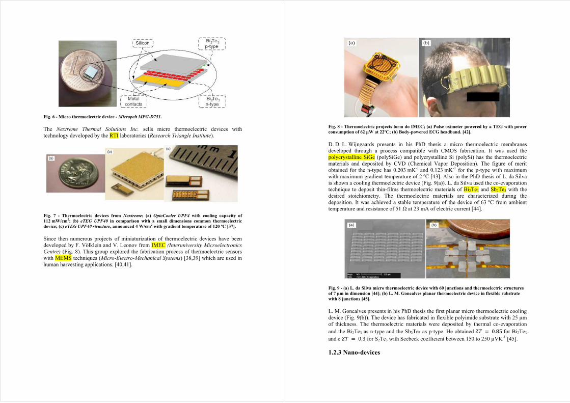
Since then numerous projects of miniaturization of thermoelectric devices have been developed by F. Völklein and V. Leonov from IMEC (Interuniversity Microelectronics
Centre) (Fig. 8). This group explored the fabrication process of thermoelectric sensors with MEMS techniques (Micro-Electro-Mechanical Systems) [38,39] which are used in human harvesting applications. [40,41].
Fig. 8 - Thermoelectric projects form do IMEC; (a) Pulse oximeter powered by a TEG with power
consumption of 62 µW at 22ºC; (b) Body-powered ECG headband. [42].
D. D. L. Wijngaards presents in his PhD thesis a micro thermoelectric membranes developed through a process compatible with CMOS fabrication. It was used the polycrystalline SiGe (polySiGe) and polycrystalline Si (polySi) has the thermoelectric materials and deposited by CVD (Chemical Vapor Deposition). The figure of merit obtained for the n-type has 0.203 mK-1 and 0.123 mK-1 for the p-type with maximum with maximum gradient temperature of 2 ºC [43]. Also in the PhD thesis of L. da Silva is shown a cooling thermoelectric device (Fig. 9(a)). L. da Silva used the co-evaporation technique to deposit thin-films thermoelectric materials of Bi2Te3 and Sb2Te3 with the desired stoichiometry. The thermoelectric materials are characterized during the deposition. It was achieved a stable temperature of the device of 63 °C from ambient temperature and resistance of 51 Ω at 23 mA of electric current [44].
Fig. 9 - (a) L. da Silva micro thermoelectric device with 60 junctions and thermoelectric structures
of 7 µm in dimension [44]; (b) L. M. Goncalves planar thermoelectric device in flexible substrate
with 8 junctions [45].
L. M. Goncalves presents in his PhD thesis the first planar micro thermoelectric cooling device (Fig. 9(b)). The device has fabricated in flexible polyimide substrate with 25 µm of thickness. The thermoelectric materials were deposited by thermal co-evaporation
and the Bi2Te3 as n-type and the Sb2Te3 as p-type. He obtained *" = 0.85 for Bi2Te3
and e *" = 0.3 for S2Te3 with Seebeck coefficient between 150 to 250 µVK-1 [45].
1.2.3 Nano-devices
The compound bismuth telluride (Bi2Te3) and antimony telluride (Sb2Te3) presents a figure of merit higher than the compound polysilicon-germanium (polySiGe) but lower operation temperature. During nearly four decades the figure of merit never passes the unit value. Then the researchers focused on increasing the figure of merit using thin-film depositions and the nano-scale phenomena. In 1993 L. D. Hicks and M. S. Dresselhaus published the theoretical models about electron confinement through quantum wells and increasing the figure of merit. This way the Seebeck coefficient is increased and reduced the thermal conductivity of the thermoelectric material [46]. R. Venkatasubramanian from RTI laboratories presents in 2001 an semiconductor
thermoelectric material p-type (Bi2Te3/Sb2Te3) in superlattices with *" = 2.4. This value inspired the researches and has completely revolutionary up to date. R. Venkatasubramanian marked them as one of the most important personalities in the thermoelectric field. He published well the approaches to increase the figure of merit: by quantum wells, superlattices and thermionic effects in heterostructures [47]. Recently he announced a thermoelectric generator with efficiency of 19 % (Fig. 10 (b)).
Fig. 10 - R. Venkatasubramanian thermoelectric projects; (a) Project presented in 2001;
(b) Thermoelectric generator presented in 2009 with efficiency of 19 % (RTI courtesy) [48].
1.3 Motivation The scientific research in thermoelectric took another interest since 1993 [46] with the introduction of nanotechnology and new horizons enabling previously unattainable by thermoelectric devices. The nano-scale phenomena began to be exploited through techniques of thin-film depositions to increase the efficiency of thermoelectric films. As presented in Fig. 11 the thermoelectric generators have been applied in several areas. The waste heat is the source with the largest range in the power range (W) that the thermoelectric devices can acquire. Space applications have great potential for application because they produce large amounts of electrical energy but presents serious risks by using radioactive materials [49]. The micro thermoelectric generators have a great potential of application in biomedical devices like the pacemaker [50] or powering wireless sensor networks (WSN) [51-55].
Fig. 11 - Power consumption scale by energy sources for thermoelectric generators [7].
Also a motivation of building a low cost chamber for deposit thermoelectric thin-films is worth. This deposition system is custom fabricated for the thermoelectric thin-films by the thermal co-evaporation technique. The necessity of build such a chamber lies on the contamination of the thermoelectric materials in the actual deposition PVD chambers. A small size chamber for depositing thermoelectric thin-films is represented in Fig. 12. The chamber needs to have performance like the complete deposition systems but with low costs. Also the thermal co-evaporation technique needs a custom configuration to obtain the right stoichiometric of the thermoelectric thin-films. The chamber was projected with a cylindrical special glass shape allowing the visualization of the process by the operator. To obtain a uniformed thin-film the chamber was projected by a rotated and heated substrate holder.
Fig. 12 – Design of a deposition chamber to deposit thermoelectric thin-films.
2 Thermoelectricity
2.1 Thermoelectricity theory The thermoelectricity consists in the conversion of temperature gradients to electric energy and it is quantified by the Seebeck coefficient () in 1822. When a material (metal or semiconductor) with a negative Seebeck coefficient is heated at one end and cooled in the other, the electrons present in the material tend to move from the hot to the cold section (Fig. 13). The hot section is in excess of ions (positively charged) while the cold is to lower energy levels. The reverse is obtained for materials with a positive Seebeck coefficient () (Fig. 14) [7,45].
Fig. 13 – Seebeck effect by demonstration the electron movement from the hot section to the cold
section.
It is reached a load balancing of the material when the electrical field obtained by the load prevents electrons movement. The Seebeck effect is the voltage obtained by the temperature difference.
Fig. 14 – Junction of two materials with negative Seebeck coefficient (on top) and positive (botton).
When the junction of two materials is covered by an electric current thermal energy is released or absorbed at this junction. The thermal energy released or absorbed is proportional to the electrical current introduced at the junction. This effect is quantified by the Peltier coefficient (') through the relationship with the Seebeck coefficient () and the temperature (") at the junction [7].
' = " , [V] (2) In terms of electrical conduction the materials can be conductors, insulators, semiconductors and superconductors. All materials have two energy bands: the valence band and conduction band (Fig. 15). There is an energy associated with each of these two bands, the valence energy (67) to the valence band and the conduction energy (69) to the conduction band. The energy gap (6:;<) is the energy between the valence and conduction bands. A metal is semiconductor if:
6:;< = 69 − 67 , [eV] (6) An insulator has a very high energy gap with makes very difficult the transfer of electrons from the valence band to the conduction band (Fig. 15(a)) [56]. As the energy gap is smaller in a semiconductor then the electrons can move from the valence band to the conduction band as a result of temperature is different from 0 K (Fig. 15(b)). In semiconductors the electrons that pass from the valence band to the conduction leave a gap in the valence band. In the conductors is not clear a separation between the valence and the conduction band (Fig. 15(c)) [56].
Fig. 15 – Structure of the energy bands; (a) Insulator; (b) Semiconductor; (c) Conductor.
In a semiconductor the temperature rising is enough for electrons to gain energy to leave the valence band to the conduction. It is known the pair electron-gap formed by a free electron in the conduction band and a hole in the valence band [56]. In the case of non-doped semiconductors (intrinsic) to move the electron from the valence band to the conduction band is necessary provide energy (6?@) greater than the energy between the two bands (6?@ > 6:;<). In an intrinsic semiconductor the number of electrons (B) that pass into the conduction band is equal to the number of gaps formed in the valence band ( C ), in other words B = C = B? . Where B? is the intrinsic concentration in a semiconductor. The intrinsic concentration depends on the energy gap (6:;< ). The electron and gap concentrations are given by:
B = C = 2 D EF"2'ℏ+H
I ( !∗ #∗ )$
% '*+ ,− ./0123456 (7)
Where 34 is the Boltzman constant, ℏ = ℎ 29: is the Planck constant, !∗ and #∗ are
the effective masses of electrons and gaps in grams (g) [56]. The effective mass of the electrons is given through [57,58]:
!∗ = ℏ;<>?;@<
, [g] (8)
And the effective mass of gaps is given by [57,58]:
#∗ = ℏ;<>A;@<
, [g] (9)
For the intrinsic semiconductors the Fermi level is given by [57]:
.BC = DEFG + $
% 345 IJ( #∗ / !∗) , [eV] (10)
At the ambient temperature $% 345 ln( #∗ / !∗) ≪ DEFG
, the Fermi level in an
intermediate point of the two bands (.BC ≈ ./01/2) [56]. The doped semiconductors (extrinsic) have filled the valence band of five or three electrons. The doping is the addition of impurities within the semiconductor. A doped semiconductor form group V elements of the periodic table is called n-type semiconductor. If the semiconductor is doped with elements from group III is called p-type semiconductor. As presented at Fig. 16 in extrinsic semiconductors the Fermi level decreases and the energy bands required for electrons to move to the conduction band to the valence are smaller. In n-type semiconductor the electron energy necessary to move to the conduction band is .N − .O and in the p-type semiconductor the energy is .0 − .P.
The Fermi level for the electrons in the extrinsic semiconductor is given by [58]:
.BO = .C + 345 IJ QRST
, [eV] (11)
Where .C is the Fermi level for intrinsic semiconductors, UV is the concentration of donor impurities. Since the Fermi level for the gaps in the extrinsic semiconductor sis given by [58]:
.B0 = .C − 345 IJ QWST
, [eV] (12)
Where UX is the concentration of acceptors impurities. In Fig. 17 is represented the junction between a p-type semiconductor with a metal and a n-type semiconductor. As can be seen in the n-type semiconductors the Fermi level lies near the conduction band and in the p-type is located near the valence band (.BO > .B0). The Fermi level in the metal (.BZ) is located between the p and n-type semiconductors [45].
Fig. 17 – Junction between p-type semiconductor with metal and n-type semiconductor.
In the region of contact of a metal with a semiconductor there is an excess of electrons and is called the region of accumulation. In Fig. 18 is represented the junction between a metal and an n-type semiconductor when traversed by an electric current (i) [59].
Fig. 18 – Junction between a metal and n-type semiconductor; (a) Absorbed heat in the junction;
(b) Released heat in the junction.
The electrons in the displacement of a region of lower energy to a region of higher energy absorb heat from the environment ([) and in the area of contact region cools the environment by the Peltier effect (Fig. 18(a)). Reversing the direction of the electric current there is in the opposite direction of electrons and release heat to the environment ([) heating the junction (Fig. 18(b)) [59].
Fig. 19 – Junction between a metal and p-type semiconductor; (a) Absorbed heat in the junction;
(b) Released heat in the junction.
In Fig. 19 is represented the junction between a p-type semiconductor with a metal when traversed by an electric current (i). When the electric current travel the junction from the metal to the p-type semiconductor, the charges moves in the same direction and the heat is absorbed from the environment ([). Heat is released in the junction to the environment when the electric current flows from the p-type semiconductor to the metal [59]. The same principle occurs in the thermoelectric device by the Peltier cooling which is made by thermoelectric structures connected in series by metal junctions (Fig. 20). The electric current enters from one the terminal and flows through all the structures and their metal contacts then exit at the other end. The n-type thermoelectric structures have a negative Seebeck coefficient (\) and the p-type have a positive.
Fig. 20 – Conventional Peltier device.
When the electric current travels the junction between the metal and the n-type semiconductor (metal-n) is released thermic energy by the Peltier effect and heats the bottom part of the device. On the top part the junctions between n-metal and metal-p is absorbed heat. In the base of the device, when the electric current flows the junction p-metal releases heat [45]. The junctions in the top part of the device absorbed heat by the Peltier effect and the junctions at the bottom part release heat [45]. There is an electrical and thermic resistance between the metal and the thermoelectric structures called the contact resistance. This contact region is created essentially by diffusion of a material junction with another material. The contact resistance (]^) is given by [45]:
]^ = _`a , [Ω] (13)
]^ is proportional to the contact resistivity (b^) and is inversely proportional to the contact area or section (c) [45]. The internal resistance (]C) of a thermoelectric device is the sum of several resistances given by [7,45]:
]C = ]S + ]1 + 4]N + 2]e , [Ω] (14)
Where ]S and ]1 represents the internal resistance of the n and p-type thermoelectric structures. ]N represents the contact resistance in the junction between the thermoelectric materials and the metal. ]e represents the internal resistance of the metal in the junction [45]. In a thermoelectric device as a generator bases in the Seebeck effect (Fig. 21). Each junction of p and n-type material (p-n junction) generates a voltage proportional to the difference in temperature between the hot and cold side.
Fig. 21 – Thermoelectric device as a thermoelectric generator.
The voltage produced in the p-n junction is smaller (in order of µV/ºC). This voltage can be multiplied by each junction in series (n) and given by [7,45]:
fghi = Jj\1 − \Sk. ∆5 , [V] (15)
Where \p and \q are the Seebeck coefficients (\) for the p and n structures. The ∆5 is the gradient temperature between the hot and cold side. The power that a thermoelectric generator can produce depends of his internal resistance (]C). This power is maximum (rsXt) when the internal resistance (]C) is equal to the load resistance (]u) and given by [7,45]:
rsXt = vwxy<%zT
= Sj|G|~k.∆i<
%jz~zG%z?zk , [W] (16)
The performance of the thermoelectric structures is measured by the value of the figure of merit (). The figure of merit is not constant with the temperature and is also designated by (5). The performance of a thermoelectric device is quantified by the coefficient of performance COP. This coefficient measures the quantity of heat absorbed by the ambient ([N) in function the quantity of electric energy consumption by the device ([!) [7,45].
r = [N[!
= j\1 − \Sk5N − 12 ]C − 3(5# − 5N)
]C + j\1 − \Sk(5# − 5N) (17)
Where 5# and 5N are the temperatures in the hot and cold sides. is the electric current and ]C is the internal resistance of the thermoelectric generator. 3 is the thermal conductivity of the thermoelectric generator. The performance of the thermoelectric thin-films is measured by the power factor given by:
r = \
b , [WKm] (18)
2.2 Thermoelectric materials The figure of merit of the thermoelectric materials has been optimized over the years (Fig. 22) by advances in research and fabrication or by the introduction of the nanotechnology [46]. The thermoelectric materials have been deposited by several deposition techniques like: flash evaporation, hot wall epitaxy, pulsed laser deposition, sputtering, metal organic chemical vapor deposition, among others. However these techniques require a long period of preparation of the materials or are relatively expensive or complicated [60].
Fig. 22 – The evolution of the figure of merit () over the years.
The superlattices structures promote the electrons mobility and gaps allowing flow of electric current. But hampers the movement of the phonons responsible of the heat transfer. In the PhD thesis of D. D. L. Wijngaards is presented the study of the figure of merit for the majority thermoelectric materials by the operation temperature (Fig. 23) [43]. The red zone in Fig. 23 represents the most common stoichiometric variations for the compounds of tellurium (Te), bismuth (Bi), antimony (Sb) and selenium (Se). These compounds present a higher figure of merit and for that reason is chosen for the majority of the thermoelectric devices.
Fig. 23 – Figure of merit vs. operation temperature of the majority thermoelectric materials [43].
2.3 Thermoelectric converters modeling In Fig. 24 is presented the thermoelectric device as a generator. The resistance represents the internal resistance of the device when is traveled through an electric current . On the left side is represented by the Seebeck effect of the voltage generated by the p-n junctions of the device ( − )( − ). The voltage generated depends on the temperature at the junction of the hot side and the temperature of the cold side [43,45]. The Peltier effect is present due to the electric current that passes between the junctions. On the right side of the block the Peltier effect of the cold junction is
represented by the current source ( − ) and for the hot junction (-). The thermal capacity equivalent to the cold junction is represented by !" and for the hot junction by ! [43,45]. The losses by convection and radiation to the ambient temperature ambient # are represented for the cold junction by $!" and for the hot junction by $! . The resistances $!,% represents the internal resistances of the thermoelectric structures [43,45]. The Joule effect for the thermoelectric structures is represented by &'. The heat fluxes due to the Joule effect for the metal contacts are
represented by &'". Finally are added to the system thermal loads to ensure the gradient temperature (&(" e &() [43,45].
Fig. 24 – Model of a thermoelectric generator [43].
2.4 Thermoelectric energy scavenging microsystem The construction of a custom deposition system allows the development of a thermoelectric microsystem in a flexible substrate. The design of the microsystem is represented in Fig. 25. The microsystem is constituted by several thermoelectric generators and a solid-state battery in flexible substrate and connected to a step-up DC-DC voltage converter. This microsystem is design to be applied in a human energy harvesting applications to power wireless sensor networks WSN and biomedical devices.
Fig. 25 – Design of an energy harvesting micro system in flexible substrate.
2.5 Voltage converters
The levels of voltage generated by most of the micro thermoelectric generators are not sufficient to power electronic devices. For the widespread use of power micro systems
need to be able to power common devices. The solution for this problem lies in the step-up DC-DC voltage converters. A model for a voltage converter to introduce in a power micro system is presented in Fig. 26.
Fig. 26 – Schematic circuit of a step-up DC-DC voltage converter [61].
The voltage conversion through the step-up DC-DC converter is done by the help of the capacitor *+- and the coil .+- . The electric current at the exit of the thermoelectric generator charges the capacitor *+- while the switch /0 is systematically closed and opened at high frequency. In the way to obtain a necessary voltage at the exit the signal of the switch need in very low duty-cycle to avoid the discharge of the capacitor *+-. When the switch /0 is open the energy storage in the coil .+- forces the discharge of the capacitor *+- by the diode 1. Finally the electric current charges the high charge capacitor *23456 and the current is rectified to the system or designed 7849:.
3 Deposition and characterization technology
3.1 Measurement system of the thermoelectric properties The electrical resistivity of the thermoelectric thin-films is measured by the van der Pauw four point probe method, and is independent of the shape of the thin-film [62]. With this method is even possible to obtain the carrier density, the mobility and also the concentration by the Hall effect through a magnetic field [63]. The system for measure the resistivity by the van der Pauw method is presented in Fig. 27.
Fig. 27 – Four point probes resistivity measurement system; (a) Top view; (b) Side view.
The method consists in the application of a known electric current in two probes and measured the voltage in the other two probes. The method is repeated in the four configurations represented in Fig. 28 and Fig. 29. By the van der Pauw method is obtained the sheet resistance 7; for a thin-film independent of the shape. It is obtained by the horizontal resistance (7=) and vertical resistance (7>). The horizontal resistance 7= value is given by:
Fig. 28 – Horizontal configuration; (a) First configuration; (b) Second configuration.
According van der Pauw the sheet resistance is related with the horizontal resistance 7= and vertical resistance 7> as follows:
By knowing the thin-film thickness (ℎ) is possible obtained the electrical resistivity by:
The error is in the order of 2r/D. The measurement of the Seebeck coefficient (M) is done by the system presented in Fig. 30.
Fig. 30 – System for measure the Seebeck coefficient (top view).
NBOPQRQS
J + NBOPQTQS
J = 1 (21)
V = 7; × ℎ , [ΩX] (22)
To obtain the Seebeck coefficient (M) is necessary a gradient temperature. The sample is placed between two plates with different temperatures. The hot plate has inside a cooper filament which serves as heater when a constant and known voltage is applied. Each plate has inside a resistance temperature detector (RTD) reference PT100 to obtain the plates temperature. The temperature sensor has a range from 0 ºC to 100 ºC. The difference in temperature is obtained by:
Where:
After obtaining the temperature in the two plates, voltage is measured in the same plates. Then the Seebeck coefficient (α) is calculated.
3.2 Thin-films deposition technology All materials are composed of atoms in constant motion, which attract each other at close range. In solid state the atoms are very close and form spatially ordered structures called lattices [64,65]. The atoms have strong force which leads to an equilibrium state. The temperature increase induces the removal of atoms together and causing the solid to be liquid if there are still cohesive forces between atoms. Further increasing temperature the atoms acquire enough kinetic energy to leave the surface of the liquid and passing into a gaseous state. With the increasing of temperature the number of atoms in the gaseous state also increases. The atoms in a gaseous state are the vapor of the substance. All the materials have a vapor pressure that is greater the higher the temperature. In the gaseous state the forces between atoms are much weaker and are more important interactions through collisions. The collisions depend on the number of atoms per unit volume or numeric density and particles energy. The energy is related to the temperature of the gas where the pressure is a very important factor [64]. To obtain a thin-film deposition is necessary to control the pressure inside a deposition chamber. The deposition of a material occurs by heating the material to be deposited. Where it changes its phase from solid to liquid and then to a gaseous state. Sometimes occurs a sublimation of a material which consists in the transition from solid state to gaseous state without passing through the liquid state [65]. In the deposition the material particles moves in all directions and are deposited on the substrate. Normally the substrate is parallel to the charge (deposition material) which it is the shortest way that the particles have to go. The position of the substrate induces a uniform thickness of the material deposited on its surface. And to obtain a desire deposition of a material is primary necessary to consider the tension pressure and is temperature on a certain pressure. In Table 1 are presented the proprieties of most common deposited materials.
7 = 7Z(1 + \@^ − \A^A) , [Ω] (23)
7Z = 100 Ω; \@ = 3,90802 XO@; \A = 0,5802 iO@.
Table 1 – Common materials proprieties for deposition [66,67].
Material Density
(g/cm3)
Fusion
temp.
(ºC)
Temperature (ºC)
@ Pressure (mbar)
Deposition
technique
10-8
10-6
10-4
e-beam Thermal
evap.
Aluminum (Al) 2.7 660 677 821 1010 Excellent Bar
Antimony (Sb) 6.62 631 279 345 425
Weak Boat Sublimes
Bismuth (Bi) 9.8 271 330 410 520 Excellent Boat
Cooper (Cu) 8.94 1083 727 857 1017 Excellent Boat, wire
To obtain a pure deposition chamber is necessary to extract the gas inside with vacuum pumps. The first vacuum pump was invented by Otto von Guericke in 1650 and published in 1672 [68]. All actual vacuum pumps are based on positive displacement which involves the mechanical movement of a piston, vanes, diaphragm or a suction system to extract the gas inside the chamber. The vacuum pumps have three stages: a capture of a certain gas volume, the compression, and the expulsion the same gas [69].
Fig. 31 – Operating pressure of different types of vacuum pumps.
Generally, the deposition of materials can be made by physical vapor deposition PVD or by chemical vapor deposition CVD. The most common physical deposition techniques are the thermal evaporation with the variations of flash evaporation and co-evaporation, e-beam (electron beam) and sputtering, among others.
Fig. 32 – Typical PVD deposition system.
In Fig. 32 is represented the typical PVD deposition system with a deposition chamber and vacuum pump connected in series to control the pressure inside. The charge is inside a crucible and when the deposition starts also is deposited in the mass sensor. The mass sensor typically is located near the substrate. Is constituted by a piezoelectric crystal which during the deposition is vibrating and is possible to obtain the deposition rate and thin-film thickness [64,65,70]. The thermal evaporation technique is represented in Fig. 33. This technique consists in heating the charge by means a
resistance called crucible. The charge is located between the resistance and the heating is due the flow of electric current. This method is simple and cheap, but presents the inconvenience of projecting impurities or other contaminants present in the crucible.
Fig. 33 – Thermal evaporation technique.
In Fig. 34 is represented he flash evaporation technique and as the name indicates is a technique where the evaporation of the material to be deposited is processed very quickly and at high temperatures. The charge is placed in a reservoir on top of the crucible. The crucible is heated by a power source and the charge falls by a gutter into the crucible. By a mechanical vibration in the gutter is controlled the material falling. This technique as the advantage of being able to deposit in small holes in great depth because de atoms have more energy than the thermal evaporation technique. All the charge evaporates which leads to a composition of the thin-film equal to the charge [65].
Fig. 34 – Flash evaporation technique.
The depositions by thermal evaporation techniques have the disadvantages of projecting impurities and others contaminants present in the filaments or boats. As well is difficultly to deposit materials with high melting temperatures at a controlled rate deposition [69]. In Fig. 35 is represented the electron beam technique (e-beam). With the e-beam technique is to deposit a large range of materials and control the deposition rate. The charge is placed in a crucible inside the evaporator. The evaporator is made of cooper (Cu) with a very good thermal conductivity and is refrigerated. Through this technique is obtained a much pure thin-film due the evaporator refrigeration which avoids the contamination by impurities from the crucible or evaporator [65,69]. The
power source used in this technique uses voltage in the range of 4 to 20 kV to heat the filament. The heated filament promotes the emission of accelerated electrons by thermionic effect. Typically the filament is coated by an oxide to promote the electron releasing in vacuum. A magnetic field is generated on top of the filament to steer the electron beam to the crucible [69]. Two problems are associated to this technique: the shifting density of the beam and the dispersion of the beam. These problems need to be resolved by the operator. The beam density can be controlled by changing the electric current of the power source. In the case of the beam is not steered to the middle of the crucible the operator change the crucible position [69].
Fig. 35 – Electron beam (e-beam) technique.
In Fig. 36 is represented the sputtering technique which allows the deposition of materials without significant change the charge (target). Contrary to the evaporation techniques the sputtering presents conformal thin-films in regions of degrees. This factor is due to the large area of the target which is not seen in the e-bam or thermal evaporation. The sputtering technique could be by direct current DC or by radio frequency RF. The DC sputtering is typically for conductive materials i.e., metals. In the case of RF sputtering is focused for nonconductive materials i.e., oxides. In the sputtering technique is necessary the entry on gases to promote the plasma. In the plasma creation is used inert gas like argon (Ar). In the reactive sputtering is used a gas which enters in the composition of the thin-film. As represented in Fig. 37 the magnetron is constituted by magnets placed on top to create a magnetic field centered to the middle of the target.
Fig. 36 – Sputtering technique.
The plasma is generated when the gas molecules ionize and charges are added or removed – like electrons – this process is called ionization. The accelerated ions beam collides with the negatively charged target. When the ions collide release atoms from the target which are deposited in the substrate [64]. In this process is produced a lot of heating in the target which is necessary a refrigeration system to maintain the target integrity. The plasma color depends on the used gas. On RF sputtering for oxides is normally used the frequency of 13,56 MHz which produces relatively lower deposition rates. The disadvantage of RF sputtering faces the DC sputtering is on the use of dielectric targets with low thermal conductivity which leads to break easily due the mechanical stress generated by cooling/heating [65].
Fig. 37 – Sputtering technique (in detail).
In Fig. 38 is presented a complete thin-film PVD deposition system.
Fig. 38 – Thin-film PVD deposition system.
In Fig. 39 are presented the techniques inside the PVD chamber shown in Fig. 38.
3.3 Thermoelectric thin-films by co-evaporation To deposit compounds, i.e., thermoelectric materials, it’s necessary deposit different materials at the same time in order to obtain the desired stoichiometry. In Fig. 40 is represented the thermal co-evaporation technique to archive compounds thin-films. Each charge have different deposition rate and is necessary a power source, a mass sensor crystal and controller for each material. By this way is possible to control the desired stoichiometry for the compound. In this technique is necessary fabricate a separation shield between the charges and has two main reasons: control the meeting
point of the two charges in the substrate, and allowing each mass sensor only read values of one material.
In Fig. 41 is presented a complete thin-film PVD thermal evaporation system for thermoelectric materials.
Fig. 41 – PVD thermal co-evaporation system.
In Fig. 42 is presented the co-evaporation technique system inside the PVD chamber shown in Fig. 41.
Fig. 42 – Thermal co-evaporation technique system (top view).
3.4 Device Patterning techniques The patterning techniques to fabricate thermoelectric structures focuses in photolithography and wet-etching techniques, using HNO3/HCl based etchants. The tentative deposition of thin-films by direct evaporation of the bulk materials - Bi2Te3 and Sb2Te3 - proved to be impossible due to the large differences in vapour pressure of bismuth (Bi), Antimony (Sb) and Tellurium (Te), resulting in a compositional gradient along the film thickness [71]. Other techniques have been reported in the literature for the deposition of telluride thin films. Co-sputtering, electrochemical deposition, metal-organic chemical vapour deposition or flash evaporation, are some examples. Concerning the use of patterning techniques on thermoelectric films, few approaches have been reported in the literature. Silva et al. [72] uses lift-off, with SU-8 photoresist, to create vertical columns of thermoelectric materials. But due to the maximum working temperature of SU-8 photoresist (≈180 ºC), thermoelectric properties of Bi2Te3 and Sb2Te3 films incorporated in the devices are worse than those obtained in bulk materials, since 200-300 ºC of substrate temperature is required to fabricate high quality thermoelectric films. Böttner et al. [73] uses dry etching to pattern thermoelectric devices. Shafai [74] reports the patterning of Bi2Te3 films by wet etching but no details are given of the process [75].
Fig. 43 – Fabrication steps of a thermoelectric cooler by patterning techniques [75]. In Fig. 43 shows the fabrication process of thermoelectric cooler. The p-type Sb2Te3 thin-film is deposited by thermal co-evaporation followed by a thin layer (100nm) of nickel (a).The thin layers of nickel are used to avoid diffusion of thermoelectric material into the next deposited layers. Photoresist (PR) is spun and p-type elements are patterned by photolithography (b),(c). Nickel is etched in a chromium etchant (Transene 1020), thermoelectric film is patterned by wet-etching in HNO3:HCl bath (d) and PR is removed. N-type film is then deposited by co-evaporation, followed by a 100 nm nickel layer (e). PR is applied and patterned by photolithography for n-type element definition (f),(g). Nickel is etched in a chromium etchant (Transene 1020), n-type film is etched in HNO3 (h) and PR removed (i). Contacts are deposited, starting with a 100 nm layer of nickel, followed by 1 μm of aluminium (j). PR is spun and contacts patterned by photolithography (k). Nickel is etched in a chromium etchant (Transene 1020), and aluminium with a standard aluminium etchant (Transene type A). PR is removed (l). A protective layer of Si3N4 can also be deposited by low-temperature hot-wire chemical vapour deposition (HW-CVD) and patterned if required, depending on the application. In Table 2 is represented the most relevant etch rates.
Table 2 – Summary of etch rates for patterning techniques [75].
Material
Etchant
Bi2Te3
Sb2Te3
Aluminum
Nickel
Al – Transene type A 8 Å /sec 5 Å /sec 10-80Å/sec < 0.1 Å/sec
3HNO3:1HCl (dil 70% H20) 2000 Å /sec 800 Å /sec < 2 Å/sec < 0.2 Å/sec
HNO3 (dil 70% H20) 2500 Å /sec 50 Å /sec < 0.1 Å/sec < 0.1 Å/sec
4 Thermoelectric thin-films by co-evaporation The proprieties of thermoelectric materials vary depending on the deposition technique chosen or the stoichiometry of the compound. In Table 3 are presented the variations of the thermoelectric materials properties by various authors and centered in compounds based in bismuth (Bi), antimony (Sb) and tellurium (Te). To obtain a thermoelectric compound is necessary knowing the materials proprieties. In Table 4 are presented the materials properties of the most common deposited materials. Generally the depositions of thermoelectric materials are in a heated substrate holder. The Bi2Te3 compound was deposited in a heated substrate at 250 ºC with a pressure of 6.1 E-7 mbar. The deposition rate for bismuth is obtained at 0.5 Å/s with 110 A of electric current and the rate for telluride is archived at 1.5 Å/s with 50 A. The Sb2Te3 compound was deposited with the substrate at 150 ºC and 1.2 E-6 mbar of pressure. The deposition rate of antimony is obtained at 1.1 Å/s with 70 A and rate for telluride is archived at 2.2 Å/s with 55 A.
Table 3 – Thermoelectric materials.
Material Resistivity
(Ωm)
Seebeck
coeff.
(µVK-1
)
Figure of
merit
(ZT)
Thermal
condutivity
(Wm-1
K-1
)
Deposition
technique Ref.
Bi2Te3 13 -228 - - Co-ev. [76]
Sb2Te3 10.4 171 - -
Bi2Te3 28.3 -228 0.28 2 Co-ev. [77]
Sb2Te3 25.5 126 0.09 2.1
Bi2Te3 9 -210 - - MOCVD [78]
Sb2Te3 3.5 110 - -
(Bi2Te3)0.9
(Bi2Se3)0.1 15 -200 0.5 1.6
Flash [79] (Bi2Te3)0.2
(Sb2Te3)0.7 12 240 0.96 1.5
Bi2Te3 21 -155 - - Co-sputt. [35]
(Bi,Sb)2Te3 23 227 - -
Bi2Te3 10 -60 - -
Electpl. [80] Bi2-
x,Sbx,Te3 - - - -
Bi2Te3 12.6 -248 0.98 1.5* Co-ev. [45]
Sb2Te3 12.6 188 0.56 1.5*
* Estimated values.
Table 4 – Seebeck coeficiente and electrical proprieties of the most common materials [7,81,82].
Material Resistivity
(x 10-8Ωm)
Electrical
conductivity
(x 10-7Ωm
-1)
Thermal
conducti.
(Wm-1
K-1
)
Seebeck
coeff.
(µVK-1
)
Figure
of merit
(ZT)
(x 10-3
)
300 K
Aluminum (Al) 2.74 3.65 237 -1.7 0.13
Cooper (Cu) 1.72 5.88 401 1.83 0.15
Lead (Pb) 21 0.48 35.3 -1.047 0.04
Chromium (Cr) 12.9 0.78 94 17.3 7.4
Molybdenum
(Mo) 5.3 1.89 138 5.57 1.27
Nickel (Ni) 7 1.43 90.9 -19.5 17.93
Gold (Au) 2.2 4,55 318 1.94 0.16
Palladium (Pd) 10.5 0.95 71.8 -9.99 3.97
Platinum (Pt) 10.4 0.96 71.6 -5.28 1.12
Silver (Ag) 1.59 6.21 429 1.51 0.1
Rhodium (Rh) 4.8 2.08 58.2 0.4 0.02
Tungsten (W) 5.3 1.89 173 1.07 0.04
Vanadium (V) 19.9 0.5 30.7 1 0.05
4.1 N-type thermoelectric thin-films made of bismuth telluride As early reported the temperature of the substrate during the deposition is a very important issue to obtain the desire stoichiometry for the compound. This temperature also influences the power factor of the thermoelectric thin-film. In Fig. 44 is presented a study of the n-type thermoelectric thin-film power factor as function of substrate temperature during the deposition. In Fig. 45 is presented power factor of the n-type thermoelectric thin-films as function of Te composition.
Fig. 44 - Power factor of Bi2Te3 thin-films as function of substrate temperature [83].
Fig. 45 – Power factor of Bi2Te3 thin-films as function of Te composition, obtained by EDX [83].
4.2 P-type thermoelectric thin-films made of bismuth telluride The study of characterization power factor of p-type thermoelectric thin-films is presented in Fig. 46.
Fig. 46 – Power factor of Sb2Te3 thin-films as function of substrate temperature and as function of
Te composition, obtained by EDX [84].
4.3 Thermoelectric devices The developed thermoelectric devices were obtained through shadow masks presented in Fig. 47. The technique of shadow masks are simple and well used in thin-film depositions were the precision distance is not critical. The distance of p-type and n-type deposited thin-films are 500 µm. The contact area of the thermoelectric structures is 1 mm2. The aluminum metal contacts have 7 mm2 of area.
Fig. 47 – Shadow masks to obtain the thermoelectric device.
The developed thermoelectric devices are presented in Fig. 48.
Fig. 48 – Developed thermoelectric devices in polyimide foil of 50 µm of thickness.
4.4 Why Scanning Probe? The local resolution of the Seebeck coefficient () is a measure for different electrically active components in materials. This becomes important especially investigating
functionally graded material. A scanning Seebeck microprobe is a device for measuring the Seebeck coefficient ( ) on a sample surface spatially resolved to achieve information on the homogeneity or distribution of the components. The Seebeck coefficient () is a measure of the electrically active components in a material. Different components in a single unit become visible by measuring the local () with a scanning thermoprobe. This applies accordingly for the electrical conductivity ( ) and therefore the behaviour of the material in a certain temperature gradient becomes predictable. A scanning Seebeck microprobe is presented in Fig. 49 and combined with the measurement of the electric potential along the surface of semiconducting or metallic material [85].
Fig. 49 – Schematic of the Seebeck microprobe. The temperature of the sample and the probe tip as
well as the Seebeck voltage can be measured. The probe tip is positioned by linear stages [85].
A heated probe tip is placed onto the surface of the sample under investigation, measuring the Seebeck coefficient (). Using a specially designed sample holder, an AC current can be applied to the sample, allowing for the detection of the voltage drop between one current contact and the travelling probe tip. This voltage is proportional to the electrical conductivity ( ) at the tip position. With this technique a spatially resolved imaging of the Seebeck coefficient () as well as the electrical conductivity ( ) can be performed. Furthermore the electrical contact resistance between different materials becomes visible, e.g., in segmented thermoelectric or other devices. So far it was reported about a measurement equipment for the spatial resolution of the Seebeck coefficient () [86,87]. With this equipment it is possible to detect inhomogeneities, different phases, even different doping levels or anisotropies [66], that is hardly possible by other surface analysis methods like SEM, EDX etc. For many materials also the homogeneity of the electrical resistivity plays an important role in their performance, especially for good quality of semiconductors.
Fig. 50 – Thin-film surface image of a Seebeck coeficiente peer pixel by scanning Seebeck
microprobe [45].
The behavior of the Potential-Seebeck-Microprobe PSM consists in a heated probe tip that is positioned onto the surface of a sample. The probe is connected with a thermocouple (in this case type T, Cu-CuNi) measuring the temperature !". The sample is in good electrical and thermal contact to a heat sink and also connected with a thermocouple measuring !#. The heat flow from the probe tip to the sample causes a local temperature gradient in the vicinity of the tip. Combining the Cu-Cu and the CuNi-CuNi wires of the thermocouples a voltage $# and $" is measured yielding the Seebeck coefficient % of the sample at the position of the probe tip according to equations [85]:
And:
Yielding in:
Where &' and &'() are the Seebeck coefficients of Cu and CuNi, respectively. Mounting the probe to a three dimensional micro-positioning system (Fig. 49) allows the determination of the thermopower of each single sample position for a certain temperature range [87], in the easiest case at room temperature. The result is a two dimensional image of the Seebeck coefficient (Fig. 50) [85].
*+ = (-. − -01). (45 − 4+), [V] (24)
*5 = (-. − -0178). (45 − 4+), [V] (25)
-. =*+
*5 − *+. (-01 − -0178) + -01, [µVK
;5] (26)
Fig. 51 – Schematic of the potential probe. An electrical AC current is applied to the sample and a
probe tip scans the surface of the sample and measures the electric potential in each point resulting
in the electrical resistivity [85].
Similar to the Seebeck surface scan the electric potential can be measured. Therefore a sample holder was constructed not only to support the sample mechanically, but also to apply an electric current to the sample. A probe tip for the voltage pick-up was installed (Fig. 51). The tip´s movement by linear stages allows for scanning the sample, and the change of the electric potential can be measured along the sample. The specific resistivity can be calculated for each measurement point according to Ohm´s law with the measured voltage *, the current < applied to the sample and with the resistance > , the specific resistivity ?, the lenght @ and the cross section A of the sample [88].
With help of this tool not only the electric resistivity can be measured, but also the ohmic contact resistance between different materials, i.e., in a stacked thermoelectric device or contacts [85]. In Fig. 52 is presented the instrument of scanning probe microprobe called SPM-Potential-Seebeck Microprobe developed by D. Platzek to spatial resolution of the Seebeck coefficient and the electrical conductivity in thermoelectric thin-films. This product is sold by Panco GmbH [89].
? = >@
A, [ΩcmC] (27)
Fig. 52 – Scanning probe instrument for spatial resolution of the Seebeck coefficient and the
electrical conductivity – SPM-Potential-Seebeck Microprobe (Courtesy of D. Platzek).
References [1] TH. J. Seebeck, “Magnetische Polarisation der Metalle und Erze durch
Temperatur-Differenz”, Abhandlungen der Deutschen Akademie der Wissenschaften zu Berlin, pp. 265-373, 1822.
[2] M. Peltier, “Nouvelles Expériences sur la Caloricité des Courans Électrique”, Annales de Phys. et de Chimie., pp. 180-193, 1834.
[3] H. F. E. Lenz, “Über die Gesetze die Elektricitätsleitung in Drähten von verschieden Lange u Dicke”, Mém. Acad. St Pétersb. Sér. VI, Vol. III, 1838.
[4] A. F. Ioffe, “Semiconductor Thermoelements and Thermoelectric Cooling”, 1st Edition, Infosearch, 1957.
[5] W. Thomson, “On an Absolute Thermometric Scale founded on Carnot's Theory of the Motive Power of Heat, and calculated from Regnault's Observations”, Philosophical Magazine, 1848.
[6] W. Thomson, “On a Mechanical Theory of Thermo-Electric Currents”, Proceedings of the Royal Society of Edinburgh, Vol. III, No. 40, pp. 91-98, 1851.
[7] D. M. Rowe, “Handbook of Thermoelectrics”, 1st Edition, CRC Press, 1995. [8] Lord Rayleigh, “On The Thermodynamic Efficiency of the Thermopile”,
Philosophical Magazine Series 5, 1941-5990, Vol. XX., Issue 125, pp. 361-363, 1885.
[9] E. Altenkirch, “Uber den Nutzeffeckt der Thermosaule”, Physikalische Zeitschrifr, Vol 10, pp. 560-580, 1909.
[10] E. Altenkirch, “Electrothermische Kalteerzeugung und Reversible Electrische Heizung”, Physikalische Zeitschrifr, Vol. 12, pp. 920-924, 1911.
[11] M. Telkes, “The Efficiency of Thermoelectric Generators”, Journal of Applied Physics, Vol. 18, pp. 1116-1127, 1947.
[12] A. F. Ioffe, “Energeticheskic Osnovy Termoelektricheskikh Baterei iz Poluprovoduikov”, Academy of Sciences of the USSR, 1949.
[13] Yu. P. Maslakovets, “Heat Energy Conversion in Electrical One by Semiconductor Thermocouples”, DSc Thesis, A. F. Ioffe Physical-Technical Institute, 1949.
[14] L. S. Stilbans, “The Investigation and New Applications of Semiconductor Thermocouples”, PhD Thesis, A. F. Ioffe Physica1-Technical Institute, 1951.
[15] L. S. Stilbans, “The Investigation and Some Applications of Semiconductor Thermoelements”, DSc Thesis, A. F. Ioffe Physical-Technical Institute, 1960.
[16] M. V. Vedernikov and E. K Jordanishvili, “A. F. Ioffe and Origin of Modern Semiconductor Thermoelectric Energy Conversion”, 17th International Conference on Thermoelectrics, pp. 37-42, 1998.
[17] A. F. Ioffe, et al., “On Increasing the Efficiency of Semiconducting Thermocouples”, The Reports of Academy of Sciences USSR, Vol. 106, 1956.
[18] H. J. Goldsmid and R. W. Douglas, “The Use of Semiconductors in Thermoelectric Refrigeration”, British Journal of Applied Physics, Vol. 5, Issue l l, pp. 386-390, 1954.
[19] W. B. Pearson and W. B. Templetion, “Thermo-electricity at Low Temperatures. III. The Absolute Scale of Thermo-electric Power: a critical discussion of the Present Scale at Low Temperatures and Preliminary Mesurements Towards its Redetermination”, Proc. Royal Society A, Vol. 231, pp. 534-544, 1955.
[20] J. W. Christian, et al., “Thermo-electricity at Low Temperatures. VI. A Redetermination of the Absolute Scale of Thermo-electric Power of Lead”, Proc. Royal Society A, Vol. 245, pp. 213-221, 1958.
[21] R. B. Roberts, “Absolute scale of thermoelectricity”, Nature, Vol. 265, pp. 226-227, 1977.
[22] C. B. Vining, “Thermopower to the people”, Nature, Vol. 423, pp. 391-392, 2003.
[23] C. B. Vining, “Semiconductors are cool”, Nature, Vol. 413, pp. 577-578, 2001. [24] T. L. Charland, et. al., “Process for the preparation of thermoelectric elements”,
US Patent No. 3086068, 1963. [25] R. C. Linnon, “Method of manufacturing a thermoelectric device”, US Patent
No. 4054478, 1977. [26] K. Yamada, et al.,“Thermoelectric module unit” US Patent No. 6233944 B1,
2001. [27] IAV Gmbh, “Thermoelectrics in Motion Electric Power from Waste Heat – A
Chance for the Automotive Industry”, 1st IAV Conference on Thermoelectrics – A Chance for the Automotive Industry?, 2008.
[28] J. LaGrandeur, et al., “Vehicle Fuel Economy Improvement through Thermoelectric Waste Heat Recovery”, Proceedings of the 11th Diesel Engine Emissions Reduction (DEER) Conference, 2005.
[29] G. J. Snyder, “Small Thermoelectric Generators”, The Electrochemical Society Interface, pp. 54-56, 2008.
[30] J. A. Paradiso, and T. Starner, “Energy Scavenging for Mobile and Wireless Electronics”, PERVASIVE Computing, 2005.
[31] M. Kishi, et al., “Fabrication of a miniature thermoelectric module with elements composed of sintered Bi-Te compounds”, 16th International Conference on Thermoelectrics, 1997.
[32] D. M. Rowe, “Review Thermoelectric Waste Heat Recovery as A Renewable Energy Source”, International Journal of Innovations in Energy Systems and Power, Vol. 1, No. 1, 2006.
[33] D. M. Rowe, “Miniature Thermoelectric Convertors”, U. K. Patent No. 8714698, 1988.
[34] H. Böttner, “Micropelt® Miniaturised Thermoelectric Devices: Small Size, High Cooling Power Densities, Short Response Time”, 24th International Conference on Thermoelectrics, 2005.
[35] H. Böttner, et al., “New thermoelectric components using microsystem technologies”, Journal of Microelectromechanical System, Vol. 13 Issue 3, pp. 414-420, 2004.
[36] http://www.micropelt.com/. [37] http://www.nextreme.com/. [38] V. Leonov, et al., “Thermoelectric Converters of Human Warmth for Self-
Powered Wireless Sensor Nodes”, IEEE Sensors Journal, Vol. 7, No. 5, 2007. [39] F. Völklein, et al., “Thermoelectric microsensors and microactuators (MEMS)
fabricated by thin-film technology and micromachining”, 18th Internacional Conference on Thermoelectrics, 1999.
[40] Z. Wang, et al., “Realization of a wearable miniaturized thermoelectric generator for human body applications”, Sensors and Actuators A: Physical, Vol. 156, pp. 95–102, 2009.
[41] J. Weber, et al., “Coin-size coiled-up polymer foil thermoelectric power generator for wearable electronics”, Sensors and Actuators A: Physical, Vol. 132, Issue 1, pp. 325-330, 2006.
[42] V. Leonov, and R. J. M. Vullers, “Wearable electronics self-powered by using human body heat: The state of the art and the perspective”, Journal of Renewable and Sustainable Energy, Vol. 1, Issue 6, 2009.
[43] D. D. L. Wijngaards, “Lateral on-chip integrated Peltier elements based on polycrystalline silicon germanium”, PhD Thesis, Technische Universiteit Delft, 2003.
[44] L. da Silva, “Integrated Micro Thermoelectric Cooler: Theory, Fabrication and Characterization”, PhD Thesis, University of Michigan, 2005.
[45] L. M. Goncalves, “Microssistema termoeléctrico baseado em teluretos de bismuto e antimónio”, PhD Thesis, University of Minho, 2008.
[46] L. D. Hicks, and M. S. Dresselhaus, “Effect of quantum-well structures on the thermoelectric figure of merit”, Physical Review B, Vol. 47, Issue 19, pp. 12727-12731, 1993.
[47] R. Venkatasubramanian, et al., “Thin-film thermoelectric devices with high room-temperature figure of merit”, Nature, Vol. 413, pp. 597-602, 2001.
[48] http://www.rti.org/. [49] R. Ewell, et. al, “SP-100 Thermoelectric Cell Testing at JPL”, NASA Jet
Propulsion Laboratory. [50] R. Venkatasubramanian, et. al, “Energy Harvesting for Electronics with
Thermoelectric Devices using Nanoscale Materials”, IEEE Electron Devices Meeting, pp. 367-370, 2007.
[51] J. Heo, et al., “EARQ: Energy Aware Routing for Real-Time and Reliable Communication in Wireless Industrial Sensor Networks”, IEEE Transactions on Industrial Electronics, Vol. 5, No. 1, pp. 3-11, 2009.
[52] J. Lee, et al., “Group Connectivity Model for Industrial Wireless Sensor Networks”, IEEE Transactions on Industrial Electronics, Vol. 57, No. 5, pp. 1835-1844, 2010.
[53] Bin Lu and V. C. Gung, “Online and Remote Motor Energy Monitoring and Fault Diagnostics Using Wireless Sensor Networks”, IEEE Transactions on Industrial Electronics, Vol. 56, No. 11, pp. 4651-4659, 2009.
[54] J. P. Carmo, et al., “A 2.4-GHz CMOS Short-Range Wireless-Sensor-Network Interface for Automotive Applications”, IEEE Transactions on Industrial Electronics, Vol. 57, No. 5, pp. 1764-1771, 2010.
[55] J. Liu and J. Yao, “Wireless RF identification system based on SAW”, IEEE Transactions on Industrial Electronics, Vol. 55, No. 2, pp. 958-961, 2008.
[56] J. H. Correia and J. P. Carmo, “Introdução às Microtecnologias no Silício”, 1st Edition, Lidel, 2010.
[57] R. Lobo, “Nanotecnologia e Nanofísica”, 1st Edition, Escolar Editora, 2010. [58] J. Singh, “Semiconductors Devices: an Introduction”, McGraw Hill, 1994. [59] S. O. Kasap, “Principles of Electrical Engineering Materials and Devices”,
McGraw Hill, 2000. [60] H. Zou, et al., “Peltier effect in a co-evaporated Sb2Te3(P)-Bi2Te3(N) thin film
thermocouple”, Thin Solid Films, Vol. 408, Issues 1-2, pp. 270-274, 2002. [61] J. P. Carmo, et al., "Thermoelectric Microconverter for Energy Harvesting
Systems", IEEE Transactions on Industrial Electronics, Vol. 57, No. 3, pp. 861-867, 2010.
[62] A. A. R. Elshabini, F. D. Barlow III, “Thin Film Technology Handbook”, 1st Edition, McGraw-Hill, 1998.
[63] L. J. van de Pauw, “A method of measuring specific resistivity and hall effect of discs of arbitrary shape”, Philips Research Reports, Vol. 13, No. 1, pp. 1-9, 1958.
[64] S. A. Campbell, “The Science and Engineering of Microelectronic Fabrication”, 2nd Edition, Oxford University Press, 2001.
[65] D. M. Mattox, “Handbook of physical vapor deposition (PDV) processing: film formation, adhesion, surface preparation and contamination control”, Noyes Publications, 1998.
[66] http://www.thermionics.com/Legacy/Download/evaprate.pdf. (acedido em 20/08/2010)
[67] D. A. Glocker and S. I. Shah, “Handbook of Thin Film Process Technology”, Institute of Physics Publishing, 1995.
[68] Ottonis de Guericke, “Experimenta Nova (ut vocantur) Magdeburgica De Vacuo Spatio”, Amsterdam J. Jansson à Waesberge, 1672.
[69] M. Ohring, “Materials Science of Thin Films”, 2nd Edition, Academic Press, 2001.
[70] A. E. Riad and F. D. Barlow III, “Thin Film Technology handbook”, McGraw-Hill, 1998.
[71] Luciana W. da Silva and Massoud Kaviany, “Miniaturized Thermoelectric Cooler”, ASME’02, New Orleans, USA, Nov 17-22, 2002.
[72] Luciana Wasnievski da Silva, Massoud Kaviany, Fabrication and Measured Performance of a First-Generation Microthermoelectric Cooler, J. of Microelectromechanical Systems, v. 14, 5 (2005) pp. 1110,.
[73] Harald Böttner, et. Al., New Thermoelectric Components Using Microsystem Technologies, Journal of Microelectromechanical Systems, 13 (2004) pp. 414-420.
[74] Cyrus Shafai, Fabrication of a micro-Peltier device, National Library of Canada (1998) pp. 76,
[75] L. M. Goncalves, et al., “Thermoelectric Micro Converters for Cooling and Energy Scavenging Systems”, Journal of Micromechanics and Microengineering, Vol. 18, No. 6, 2008.
[76] H. Zou, “Preparation and Characterization of bismuth Telluride and antimony telluride thermoelectric thin films”, Phd Thesis, Cardiff UK, 2003.
[77] L. da Silva, “Micro Thermoelectric Cooler Fabrication: Growth and Characterization of Patterned Sb2Te3 and Bi2Te3 Films” 22th International Conference on Thermoelectrics, 2003.
[78] A. Giani, et al., “Growth of Bi2Te3 and Sb2Te3 thin films by MOCVD”, Materials Science and Engineering: B, Vol. 64, Issue 1, pp. 19-24, 1999.
[79] A. Foucaran, et al., “Flash evaporated layers of (Bi2Te3–Bi2Se3)(N) and (Bi2Te3-Sb2Te3)(P)” Materials Science and Engineering B, Vol. 52, Issues 2-3, pp. 154-161, 1998.
[80] J. R. Lin, et al., “Thermoelectric Microdevice Fabrication Process and Evaluation at the Jet Propulsion Laboratory (JPL)”, 21th International Conference on Thermoelectrics, 2002.
[81] C. Kittel, “Introduction to Solid State Physics”, John Wiley, 1986. [82] http://www.goodfellow.com/. [83] L.M. Goncalves, et al., “Optimization of thermoelectric properties on Bi2Te3
thin films deposited by thermal co-evaporation”, Thin Solid Films, Vol. 518, pp. 2816-2821, 2010.
[84] L.M. Goncalves, et al., “Thermal co-evaporation of Sb2Te3 thin-films optimized for thermoelectric applications”, Thin Solid Films, Vol. 519, pp. 4152-4157, 2011.
[85] D. Platzek, et al., “Potential-Seebeck-Microprobe (PSM): Measuring the Spatial Resolution of the Seebeck Coefficient and the Electric Potential”, Proc. of 24th International Conference on Thermoelectrics (ICT 2005), pp. 13-16, 2005.
[86] P. Reinshaus, et al., Proc. 2nd Europ. Symposium on Thermoelectrics-Materials, Processing Techniques, and Applications, Dresden, Germany, pp. 90, 1994.
[87] D. Platzek, et al., “An Automated Microprobe for Temperature Dependent Spatial Scanning of the Seebeck Coefficient“, Proc. 22nd International Conference on Thermoelectrics (ICT2003), pp. 528-531, 2004.
[88] D. Platzek, et al., “Anisotropy of the Seebeck Coefficient Detected by the Seebeck Scanning Microprobe“, Proc. 8th European Workshop on Thermoelectrics, 2004.