74
1 Microcontrollers Class : 4 th Semister E&C and EEE Subject Code: 06ES42 Chapter : UNIT 1-2 Class : 2 Date : 15 th Feb 2010 D R Subramanyam [email protected]

1
Microcontrollers
Class : 4th Semister E&C and EEESubject Code: 06ES42Chapter : UNIT 1-2Class : 2
Date : 15th Feb 2010
D R Subramanyam [email protected]

Revision of Previous Class topics
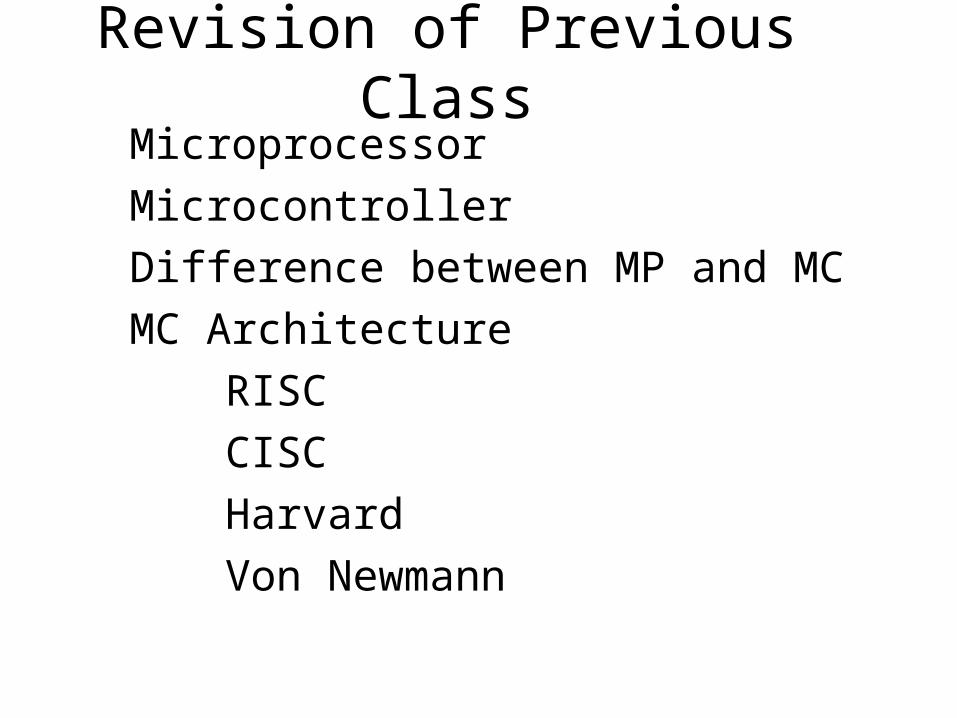
Revision of Previous ClassMicroprocessor
Microcontroller
Difference between MP and MC
MC Architecture
RISC
CISC
Harvard
Von Newmann

4
Microprocessors “A microprocessor is a multipurpose, programmable, clock
driven, register – based electronics device that reads binary instructions from a storage device called memory, accepts binary data as input and processes data according to those instructions and provides results as output”
• Example : Intel’s x86, Motorola’s 680x0
CPU
General-Purpose Micro-processor
RAM ROM I/O Port
TimerSerial COM Port
Data Bus
Address Bus
General-Purpose Microprocessor System
Many chips on mother’s board

5
Microcontroller:
• A smaller computer• On-chip RAM, ROM, I/O ports...• Example : Motorola’s 6811, Intel’s 8051, Zilog’s Z8X and PIC 16X
RAM ROM
I/O Port
TimerSerial COM Port
Microcontroller
CPU
A single chip

6
Microprocessor vs Microcontroller
Microprocessor
• CPU is stand-alone, RAM, ROM, I/O, timer are separate
• designer can decide on the amount of ROM, RAM and I/O ports.
• expensive• versatility • general-purpose
Microcontroller
• CPU, RAM, ROM, I/O and timer are all on a single chip
• fix amount of on-chip ROM, RAM, I/O ports
• for applications in which cost, power and space are critical
• single-purpose

7
RISC (Reduced Instruction Set Computing Processor)

8
CISC (Complex Instruction Set Computing Processors)
• Numerous Instruction Group• Numerous Addressing Modes• Microcoded Instructions• Microcontrollers and Microprocessors are
CISC based.• DSP’s are closer to RISC.

9
Von Newmann Architecture

10
Harvard Architecture

11
Let us know more about Microcontrollers

12
Microcontroller’s internal Blocks
• CPU ( ALU, Registers, Oscillator/clock, Bus control)• RAM /Data memory• ROM / program memory• I/O ports• Timer/counters• Serial ports• Interrupts

13
Let us put together all what we discussed

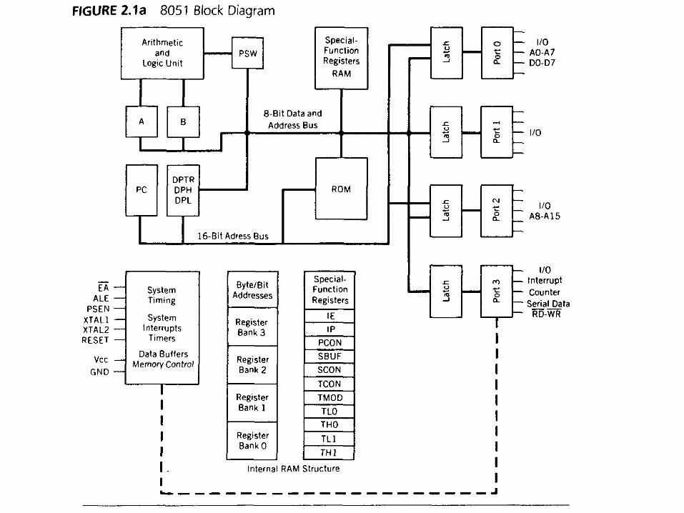
Microcontroller Block Diagram
CPU
On-chip RAM
On-chip ROM for program code
4 I/O Ports
Timer 0
Serial PortOSC
Interrupt Control
External interrupts
Timer 1
Timer/Counter
Bus Control
TxD RxDP0 P1 P2 P3
Address/Data
Counter Inputs

15
Microcontroller Block Diagram
ALU
Internal ROM
I/O Ports
Internal RAM
AccumulatorRegisters
Program CounterStack Pointer
Oscillator
Counter/Timer
Serial Port
Interrupt Logic
Bus Control


The 8051 Oscillator and Clock

Program Counter and Data pointer
Program Counter (PC):
Program counter is a 16 bit Register. It holds the address of the next instruction to be executed.
It does not have internal address (PC is the only register not having the internal address)
Data Pointer (DPTR): DPH and DPL
DPTR is used to furnish memory address for internal and external code access and external data access

A and B CPU Registers
• A and B registers are the two registers among the 34 general purpose registers
• Holds results of many instructions, particularly math and logical operations
• A register (Accumulator) is the most versatile and is used for many operations including addition, subtraction, integer multiplication and division and Boolean bit manipulations
• A register is also used for all data transfer between 8051 and any external memory
• B register is used with A register for multiplication and division operations.

Flags and Program Status Word (PSW)

Internal MemoryInternal RAM - 128 bytes 00H to 7FHInternal ROM - 4 K Bytes 000H to FFFH

Internal RAM


The Stack and Stack pointer(SP)Stack area:Part of Internal RAMIt is limited in height to the size of internal RAM
Stack Pointer (SP): 8 bits wideIncrements unlike many microprocessors where SP decrementsOn RESET it is et to 07H

The Stack and Stack pointer(SP)

Special Function Registers(SFRs)

Special Function Registers(SFRs)
Note: Program Counter Register is not a special function Register

Special Function Registers

Special Function Registers-Continued

Internal ROM

Input / Output Pins, Ports and Circuits

A Pin of Port 1
8051 IC
D Q
Clk Q
Vcc
Load(L1)
Read latch
Read pin
Write to latch
Internal CPU bus
M1
P1.X pinP1.X
TB1
TB2
P0.x

Writing “1” to Output Pin P1.X
D Q
Clk Q
Vcc
Load(L1)
Read latch
Read pin
Write to latch
Internal CPU bus
M1
P1.X pinP1.X
8051 IC
2. output pin is Vcc1. write a 1 to the pin
1
0 output 1
TB1
TB2

Writing “0” to Output Pin P1.X
D Q
Clk Q
Vcc
Load(L1)
Read latch
Read pin
Write to latch
Internal CPU bus
M1
P1.X pinP1.X
8051 IC
2. output pin is ground1. write a 0 to the pin
0
1 output 0
TB1
TB2

Reading “High” at Input Pin
D Q
Clk Q
Vcc
Load(L1)
Read latch
Read pin
Write to latch
Internal CPU bus
M1
P1.X pin
P1.X
8051 IC
2. MOV A,P1
external pin=High1. write a 1 to the pin MOV
P1,#0FFH
1
0
3. Read pin=1 Read latch=0 Write to latch=1
1
TB1
TB2

Reading “Low” at Input Pin
D Q
Clk Q
Vcc
Load(L1)
Read latch
Read pin
Write to latch
Internal CPU bus
M1
P1.X pin
P1.X
8051 IC
2. MOV A,P1
external pin=Low1. write a 1 to the pin
MOV P1,#0FFH
1
0
3. Read pin=1 Read latch=0 Write to latch=1
0
TB1
TB2

Other Pins
• P1, P2, and P3 have internal pull-up resisters.– P1, P2, and P3 are not open drain.
• P0 has no internal pull-up resistors and does not connects to Vcc inside the 8051.– P0 is open drain.– Compare the figures of P1.X and P0.X.
• However, for a programmer, it is the same to program P0, P1, P2 and P3.
• All the ports upon RESET are configured as output.
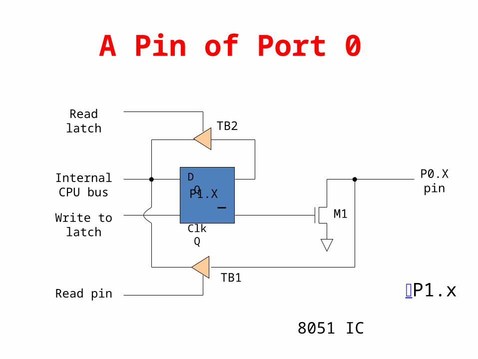
A Pin of Port 0
8051 IC
D Q
Clk Q
Read latch
Read pin
Write to latch
Internal CPU bus
M1
P0.X pinP1.X
TB1
TB2
P1.x
Input/Output Pins, Ports and CircuitsControl Signals
Address/Data

Input/Output Pins, Ports-PORT0
Control Signals
Address/Data

Input/Output Pins, Ports-PORT1

Input/Output Pins, Ports-PORT2

Input/Output Pins, Ports-PORT3

External Memory

External Memory Timing Wave Forms

Counters and Timers

Timer :

Counting

TCON-Timer Control SFR
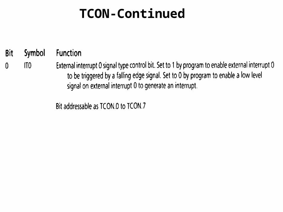
TCON-Continued

TMOD-Timer Mode Control SFR
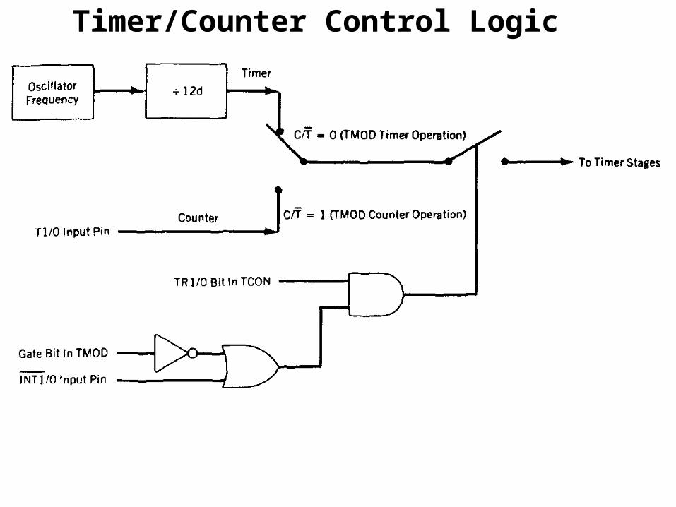
Timer/Counter Control Logic

Timer Modes of Operation
Timer Mode 0
Timer Mode 1
Timer Mode 2
Timer Mode 3
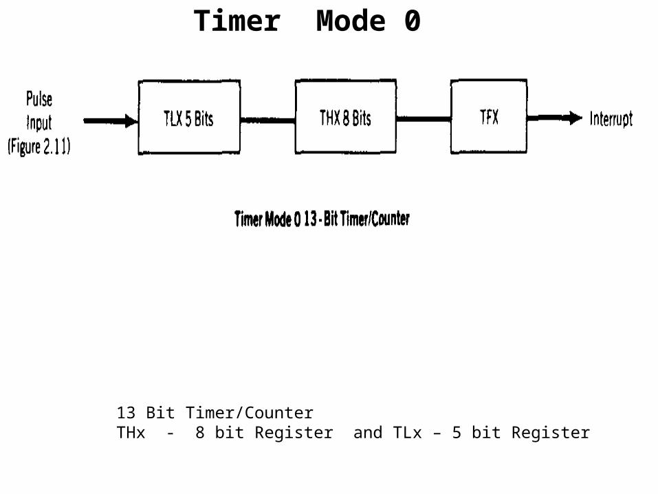
Timer Mode 0
13 Bit Timer/CounterTHx - 8 bit Register and TLx – 5 bit Register

Timer Mode 1
16 Bit Timer / counterTMOD = 01bThe Timer Flag would be set in 1311 seconds using a 6 MHz Crystal

Timer Mode 2
This mode exhibits auto reload feature

Timer Mode 3
Timer 1 can still be used but interrupt feature can not be used

Serial Data Input/Output
Registers used for Serial CommunicationSBUF-Serial Buffer registerSCON-Serial Control registerPCON-Power Control register

SCON-Serial Port Control SFR

PCON-Power Mode Control SFR

Serial Communication Continued
Serial InterruptsData Transmission Data Reception
Baud rate is set using Timer 1Whenever serial port is used in Mode 1 or 3 Timer 1 can not be used for any other purpose other than generating Baud clock

Shift Register Mode 0 Timing

Standard UART data word

Multi Processor Data Word

Interrupt :

Interrupts
1. Enabling and Disabling Interrupts
2. Interrupt Priority
3. Writing the ISR (Interrupt Service Routine)

IE register

IP register

Interrupt VectorsInterrupt Vector Address
System Reset 0000H
External 0 0003H
Timer 0 000BH
External 1 0013H
Timer 1 001BH
Serial Port 0023H
Timer 2 002BH

Reset

Summary

8051 µC Hardware


