Page 1
1
MOST Moderate-Weak Inversion Region as the
Optimum Design Zone for CMOS 2.4-GHz
CS-LNAsRafaella Fiorelli, Fernando Silveira and Eduardo Peralıas
Abstract
In this paper, the MOS transistor (MOST) moderate-weak inversion region is shown to be the optimum
design zone for CMOS 2.4-GHz common-source low noise amplifiers (CS-LNA) focused on low power
consumption applications. This statement is supported by a systematic study where the MOST is ana-
lyzed in all-inversion regions using an exhaustive CS-LNA noise figure-power consumption optimization
technique with power gain constraint. Effects of bias choke resistance and MOST capacitances are
carefully included in the study to obtain more accurate results, especially for the moderate-weak inversion
region. Noise figure, power consumption and gain versus the inversion region are described with design
space maps, providing the designer with a deep insight of their trade-offs. The Pareto-optimal design
frontier obtained by calculation, -showing the moderate-weak inversion region as the optimum design
zone- is re-verified by extensive electrical simulations of a high number of designs. Finally, one 90-nm
2.4-GHz CS-LNA Pareto optimal design is implemented. It achieves the best FoM considering under-mW
CS-LNAs published designs, consuming 684 µW, a noise figure of 4.36 dB, a power gain of 9.7 dB and
an IIP3 of -4 dBm with load and source resistances of 50 Ω.
Index Terms
CS-LNA, Moderate Inversion, Weak Inversion Noise figure, Optimization, Low power, gm/ID,
Design Methodology, Pareto optimal.
I. INTRODUCTION
The increase of radiofrequency (RF) applications focused on low power, short range and low rate, such
as those that meet ZigBee or low-energy Bluetooth standards, are forcing the industry to develop low-cost
chip solutions. This cost reduction is mainly achieved by using CMOS technology and reaching short-
time-to-market designs, where a prior knowledge of the circuits behavior considerably helps. Biasing the
October 6, 2014 DRAFT
Page 2
2
MOST in weak (WI) and moderate (MI) inversion region instead of strong inversion (SI) is necessary
to achieve the mentioned power reduction of orders of magnitude [1]; however, the effect of moving to
MI and WI means an increment in the parasitic capacitances and a reduction in the transition frequency
fT , hence, in the maximum working frequency. For the nanometer CMOS technologies used today, it is
possible to bias the MOST in MI-WI region when working in the GHz-range, where the conservative
quasi-static limit of one-tenth of fT is yet valid. Various CMOS analog RF designs biased in MI and
WI have been reported, as shown in [2]–[11], among others, where a considerable power reduction is
achieved compared with biasing in strong inversion. However, there is a lack of published works that
systematically study all-inversion regions of MOST for RF design, going farther than just showing the
feasibility of a particular design and find the optimum design zone for certain constraints. This deficiency
is notorious in LNAs, as in CS-LNAs.
In this paper, we consider the CS-LNA optimum in the sense of Pareto noise figure-power consumption
optimal frontier with gain constraint, input/output LNA impedance matching and without tight linearity
requirements, to cope with the before mentioned standards. All regions of operation of the MOST
are systematically analyzed to prove the narrowband RF under-mW 2.4 GHz CS-LNAs optima lay in
the moderate-weak inversion region. Finding this Pareto frontier without using electrical optimization
tools implies the implementation of an optimization method that considers the inversion region as its
core variable. In this sense, this paper follows the same approach of [10]–[20], where optimization
techniques for RF circuits applied before electrical simulation are proven as a suitable design strategy.
Particularly for CS-LNA, well-known optimization techniques have been presented, as in [12]–[14],
but these techniques only cover the strong inversion region, do not study the effects of CS-LNA output
impedance in the optimization process and disregard the inductors parasitics. Our approach, which expands
previous studies, helps the designer to give a deep insight into the behavior of low-power CS-LNAs
fundamental characteristics as well as their trade-offs, which helps in reducing consumption without
losing gain, noise or linearity performance.
To demonstrate that optimal designs of 2.4-GHz CS-LNAs are in the moderate-weak inversion region,
we need to systematically study the MOST in all regions of operation: weak, moderate and strong
inversion, finding the best design in each case. Although the authors know that more efficient optimization
algorithms exist to cope with multi-objective optimization, our approach allows us not only to find the
Pareto frontier but also to study in detail the evolution of the LNA characteristics in all regions as well
as the arising compromises, as we will see later on.
The use of the gm/ID ratio [21], [22] is our fundamental tool to cover all-inversion regions of the
October 6, 2014 DRAFT
Page 3
3
MOST. Its election is principally due to it being a good indicator of the inversion region because of
the very small range of gm/ID values, as they are in the order of 1 V −1 to 30 V −1 for a nanometer
bulk MOST. In fact, as a rule of thumb [23], for our RF 90-nm CMOS 1-Poly 9-Metals process, called
from now on Reference Technology, WI is considered for gm/ID values well above 20 V −1, SI is well
below gm/ID=10 V −1 and MI is in the midst of them. Also, the gm/ID ratio of a saturated MOST
has a biunivocal relation with the normalized current or current density, defined as i = ID/(W/L) [21],
with ID, W and L the MOST drain current, width and length, respectively. Since i versus gm/ID is
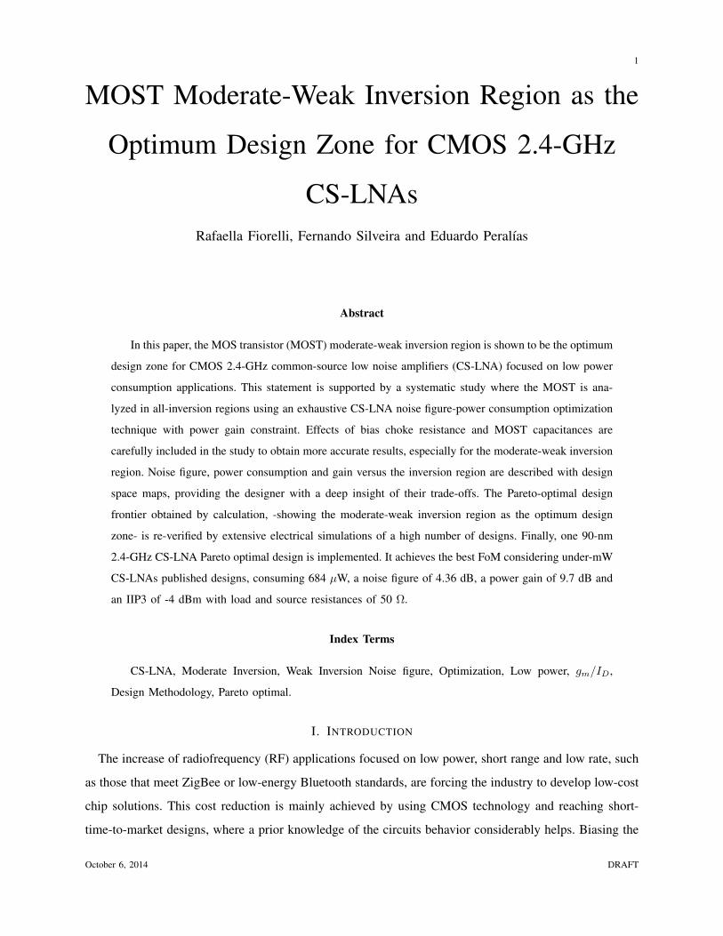
quasi-independent of VDS and W for L-constant MOST (see Fig. 1(a) ), given gm/ID and ID, the size
of MOST is fixed.
The proposed approach considers input/output LNA impedance matching to find the MOST operation
point and all components’ geometries that minimize its noise figure for each quiescent current ID, with
a specific power gain constraint. In this paper, the design method used follows the guidelines the authors
enunciate in [10]; i.e. the application of semi-empirical modeling for RF devices (in particular MOST
and inductors) and the use of analytical expressions of circuit’s small-signal model in a developed ad-hoc
design flow which arrange them together with the necessary decisions fixed by LNA specifications and
technological constraints.
The search of the optimum in all-inversion regions needs a reasonably accurate MOST model, especially
in MI and WI regions. It oblige us to use not only the intrinsic capacitances (considered for this study
only the five quasi-static capacitances1), but also the extrinsic ones, even the generally disregarded, as
Cds. Analogously, for passive components such as inductors, their parasitics cannot be ignored in a
first approximation. Additionally, noise figure computation takes into account noise parameters variations
with the MOST transistor inversion region and includes the noise due to bias choke resistor. Moreover, to
correctly compute power gain, an accurate value of the CS-LNA output impedance is deduced. Finally,
the layout effects are incorporated in the carried out optimization because semi-empirical models of the
used RF devices contain this information from the foundry.
To sum up, the new ideas of this paper are the following: (1) to show that the optimum design zone
for CS-LNAs, for 2.4 GHz ISM band, is the MOST moderate-weak inversion region; (2) the systematical
study of the design trade-offs among power consumption, noise, gain and element sizing among all MOST
inversion regions; (3) the assertion that good designs are obtained when working with low currents and
1The hypothesis of the MOST operation below the quasi-static limit of one tenth of the transition frequency fT [24] is valid
for the considered working frequency and process.
October 6, 2014 DRAFT
Page 4
4
Fig. 1. (a) i and gds/ID (inner plot) and (b) C′gs for a wide set of nMOST finger widths Wf and number of fingers nf versus
gm/ID . (c) Typical noise parameters γ, α (and γ/α) for all-inversion regions.
in MI-WI regions; (4) the need of have a limited set of parametrized models, simple yet accurate, for
the circuit’s elements (particularly for MOST and inductors).
The outline of this paper is as follows. Section II describes the MOST and passive components
modeling. Section III provides the small-signal LNA analysis. Section IV details the CS-LNA optimization
methodology and provides the Pareto optimal LNA design’s frontier, also presents the validation technique
via several CS-LNA designs and the gathered conclusions. Section V shows the measurements of a
fabricated 2.4-GHz 90-nm CS-LNA. Finally, Section VI summarizes the main contributions of this paper.
II. RF DEVICE MODELS
A. MOST model
Modeling of MOST is done by using a semi-empirical model based on a lookup-table (LUT) [10],
[22], [25] obtained by electrical DC and noise simulations, performed only once, on models qualified by
the foundry of our Reference Technology. This way, it jointly considers second and higher order effects
that appear in nanometer technologies, as discussed in [10]. The MOST model specifically includes the
October 6, 2014 DRAFT
Page 5
5
following characteristics as a function of gm/ID: (1) normalized current i; (2) output conductance to
current ratio gds/ID; (3) normalized MOST capacitances C ′ij = Cij/W with ij=gs, gd, gb, bs, bd;
and (4) drain white noise parameters. The extrinsic capacitances and the gate resistance, RgMOS , are
considered constants for all inversion regions but dependent on the MOST geometry (e.g. in our case
RgMOS ≈ 4.3+78/nf , with nf the MOST number of fingers). The capacitance normalization of item (3)
can be performed because intrinsic capacitances as well as the extrinsic part of gate-source and gate-drain
ones are proportional to W , and MOST length is always fixed equal to the minimum Lmin=90 nm (the
extrinsic part of the gate-bulk capacitance is disregarded). Features (1) and (2) are presented in Fig. 1(a).
An example of item (3) is in Fig. 1(b), where C ′gs is plotted for a wide range of MOST widths. Its spread
for a fixed inversion level is around 10%, which is acceptable for our purposes. For the rest of normalized
capacitances, the variation is below this value (C′
gd ≈ (0.36±0.03) fF/µm, C′
gb < (0.03±0.03) fF/µm,
C′
ds ≈ 0.09 fF/µm, and C′
bs ≈ C′
bd ≈ 0.34 fF/µm). All LUTs capacitances are estimated by electrical
DC simulations. The second-order dependence on VDS voltage of items (2) and (4) is also considered
in the correspondent LUTs. Parameter gmb is also modeled, being its dependence practically linear with
gm/ID(gmb/ID ≈0.13 gm/ID
).
MOST drain white noise is the CS-LNA highest noise contributor at the working frequencies. Its
power spectral density (psd) is modeled with i2w,d = 4kBTγαgm, with kB the Boltzmann constant, T
the absolute temperature, γ the excess noise factor [12] and α = gm/gd0, being gd0 the zero-VDS bias
drain conductance [24]. Extraction of γ, α and the relation γ/α versus gm/ID via electrical simulations
generates the curves of Fig. 1.(c). In this case the generally used values of γ ∼=2/3 and α ∼=0.6 do not
adjust to the extracted data, in particular for MI and WI regions. Additionally, the induced-gate noise
psd is modeled as i2g = 165 π
2kBTαδC2
gs
gmf2, where δ is the gate noise coefficient [12], considered here an
independent parameter equal to 4/3.
B. Passive Components models
Three types of passive components are used in our designs: inductors, capacitors and resistors. For our
Reference Technology, we obtain their models just once from AC electrical simulations at the working
frequency ω0 = 2πf0, saving them in LUTs. The simulation extracts the equivalent element’s value
together with their equivalent parasitics, from which their quality factors are computed. To speed-up the
design flow, all passive elements are selected from a parameterized library provided and characterized
by the foundry up to 20 GHz [25].
Inductor model consists of an equivalent inductor with a parasitic resistor, either in parallel or in series,
October 6, 2014 DRAFT
Page 6
6
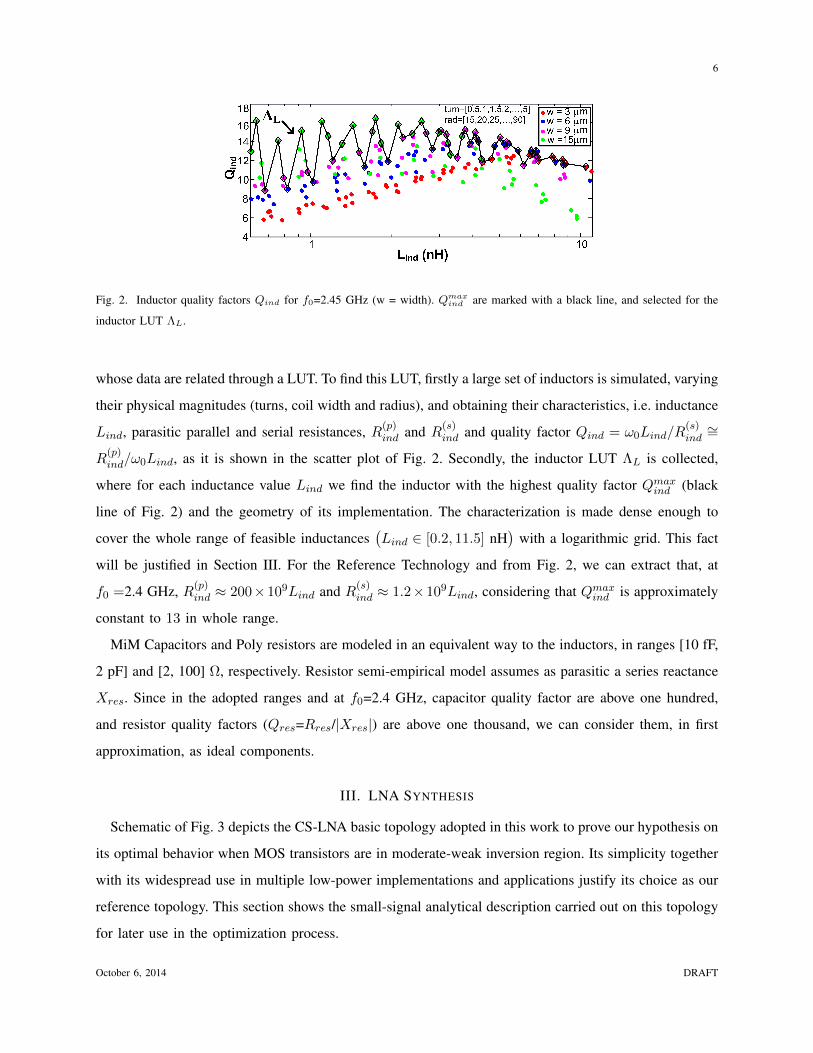
Fig. 2. Inductor quality factors Qind for f0=2.45 GHz (w = width). Qmaxind are marked with a black line, and selected for the
inductor LUT ΛL.
whose data are related through a LUT. To find this LUT, firstly a large set of inductors is simulated, varying
their physical magnitudes (turns, coil width and radius), and obtaining their characteristics, i.e. inductance
Lind, parasitic parallel and serial resistances, R(p)ind and R(s)
ind and quality factor Qind = ω0Lind/R(s)ind∼=
R(p)ind/ω0Lind, as it is shown in the scatter plot of Fig. 2. Secondly, the inductor LUT ΛL is collected,
where for each inductance value Lind we find the inductor with the highest quality factor Qmaxind (black
line of Fig. 2) and the geometry of its implementation. The characterization is made dense enough to
cover the whole range of feasible inductances(Lind ∈ [0.2, 11.5] nH
)with a logarithmic grid. This fact
will be justified in Section III. For the Reference Technology and from Fig. 2, we can extract that, at
f0 =2.4 GHz, R(p)ind ≈ 200×109Lind and R(s)
ind ≈ 1.2×10⁹Lind, considering that Qmaxind is approximately
constant to 13 in whole range.
MiM Capacitors and Poly resistors are modeled in an equivalent way to the inductors, in ranges [10 fF,
2 pF] and [2, 100] Ω, respectively. Resistor semi-empirical model assumes as parasitic a series reactance
Xres. Since in the adopted ranges and at f0=2.4 GHz, capacitor quality factor are above one hundred,
and resistor quality factors (Qres=Rres/|Xres|) are above one thousand, we can consider them, in first
approximation, as ideal components.
III. LNA SYNTHESIS
Schematic of Fig. 3 depicts the CS-LNA basic topology adopted in this work to prove our hypothesis on
its optimal behavior when MOS transistors are in moderate-weak inversion region. Its simplicity together
with its widespread use in multiple low-power implementations and applications justify its choice as our
reference topology. This section shows the small-signal analytical description carried out on this topology
for later use in the optimization process.
October 6, 2014 DRAFT
Page 7
7
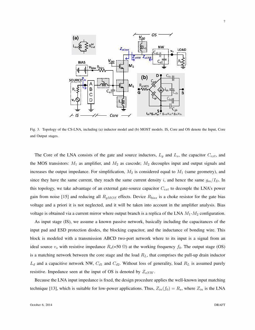
Fig. 3. Topology of the CS-LNA, including (a) inductor model and (b) MOST models. IS, Core and OS denote the Input, Core
and Output stages.
The Core of the LNA consists of the gate and source inductors, Lg and Ls, the capacitor Cext, and
the MOS transistors: M1 as amplifier, and M2 as cascode; M2 decouples input and output signals and
increases the output impedance. For simplification, M2 is considered equal to M1 (same geometry), and
since they have the same current, they reach the same current density i, and hence the same gm/ID. In
this topology, we take advantage of an external gate-source capacitor Cext to decouple the LNA’s power
gain from noise [15] and reducing all RgMOS effects. Device Rbias is a choke resistor for the gate bias
voltage and a priori it is not neglected, and it will be taken into account in the amplifier analysis. Bias
voltage is obtained via a current mirror where output branch is a replica of the LNA M1-M2 configuration.
As input stage (IS), we assume a known passive network, basically including the capacitances of the
input pad and ESD protection diodes, the blocking capacitor, and the inductance of bonding wire. This
block is modeled with a transmission ABCD two-port network where to its input is a signal from an
ideal source vs with resistive impedance Rs(=50 Ω) at the working frequency f0. The output stage (OS)
is a matching network between the core stage and the load RL, that comprises the pull-up drain inductor
Ld and a capacitive network NW, Cd1 and Cd2. Without loss of generality, load RL is assumed purely
resistive. Impedance seen at the input of OS is denoted by ZoNW .
Because the LNA input impedance is fixed, the design procedure applies the well-known input matching
technique [13], which is suitable for low-power applications. Thus, Zin(f0) = Rs, where Zin is the LNA
October 6, 2014 DRAFT
Page 8
8
input impedance, which includes the effects of the ABCD, Core and OS, i.e. Zin(M1,M2, Lg, Cext, Ls, Ld, Cd1, Cd2; f0;Rbias)
Inset (a) of Fig. 3 describes the inductors’ model utilized in this analytical study: its inductance Lind
jointly with the equivalent parallel resistance R(p)ind (taken from LUT ΛL detailed in Section II). Inset
(b) of Fig. 3 represents the considered model for MOS transistors. All MOST characteristics are known
when values of gm/ID and ID are given, by means of LUTs as explained in Section II. Gate resistance
RgMOS is not neglected in the model as its effects are noticeable for small-width MOST (its reduction
is reached by increasing the number of fingers nf of MOST).
Even though a simpler model for the MOST could simplify the design procedure, especially in SI and
SI-MI regions (gm/ID < 15), we must describe correctly the LNA behavior up to WI while reaching a
good precision in the MI-WI zone (gm/ID < 20). In these regions, MOSTs are so wide that parasitics,
Cgs, Cgd, Cgb, Cbs, Cbd and Cds, are not negligible, and consequently direct coupling between input and
output stages must be accurately modeled.
To achieve the input-matching goal, we need precise evaluation of LNA input impedance, Zin, Core
output impedance, ZoCore, and input impedance of OS, ZoNW . Either rational algebraic expressions
obtained via a symbolic analysis tool or subroutines that solve the complete linearized circuit are two
alternative procedures that we have successfully tested.
For the design process, we apply the gm/ID method of [21] so the pair (gm/ID,ID) are the two first
input design variables. This enable the visualization of the optimum zone and the consumption trade-off
with other CS-LNA characteristics. The last input design variable is Lg, taken from the LUT ΛL in
order to use only the best inductors available in the Reference Technology and to know in advance their
parasitics.
The unknowns to be found are W , Ls, Cext, Ld and Cd1, Cd2. To obtain them, we numerically solve
the equation system Zin = Rs, following the next Iterative Procedure, efficiently implemented using a
numerical solver in Matlab environment:
1) Fix values of (gm/ID,ID) and Lg. From the pair (gm/ID, ID) and the definition of i, W is deduced
from the LUTs of gm/ID @ i.
2) Determine two seed values for Ls and Cext, from the closed expression in (7) corresponding to the
LNA simplified scheme of Appendix A. Since both must be feasible in the technology, Ls should
be discretized to the nearest value in ΛL.
3) In this moment whole input and Core stages are fully known, i.e. Lg, Cext, Ls, and W . Then,
calculate the core output impedance ZoCore(f0).
4) Determine an output matching network, Ld and Cd1, Cd2, such as ZoCore(f0) = Z∗oNW (f0), where
October 6, 2014 DRAFT
Page 9
9
the asterisk (∗) indicates the complex conjugate operator. This network must be feasible within the
technology and some directions to obtain it are pointed in next subsection.
5) As now the whole LNA elements are known, compute Zin(f0).
6) Compare Zin with the source impedance Rs, computing S11(= |Zin −Rs|/|Zin +Rs|), and decide
if the solution is good enough, e.g. if S11 < −20 dB. If not, correct initial values of Ls (within ΛL)
and Cext by a minimization in least-squares sense , and return to Step 3).
A. Power gain
An efficient CS-LNA power transfer needs an effective load of the Core stage with a high resistive
term. Since in general the output impedance ZoCore is capacitive,(Im(ZoCore) < 0
), Ld is used to
produce a purely inductive output impedance, ZoLNA(= ZoCore||ZLd), that via the capacitive network
NW is matched to RL. This impedance transformation becomes easier when the drain inductor value is
lower, hence when the design area is smaller. However, in that case the parallel parasitic resistance, R(p)d ,
also decreases, implying a reduction in the output power or equivalently in the LNA power gain. Thus, Ld
value is a trade-off between these two conditions: acceptable area and high power gain. Mathematically,
requirements needed to find a network NW are Re(ZoLNA) ≤ RL and Im(ZoLNA) > 0, which produce
the following value for Ld:
Ld =1
ω0
(Im(1/ZoLNA) +
√GoLNA(1/ReffL −GoLNA)
) , (1)
where ReffL = Re(ZoLNA) and
GoLNA = Re
(1
ZoLNA
)= Re
(1
ZoCore
)+
1
R(p)d
(2)
Since Ld in (1) depends on GoLNA in (2), and this one depends on Ld through its parasitic R(p)d , the
value of Ld must be obtained in an iterative way. Also, it must verify, Ld ≤ Lmaxind , where Lmaxind is the
maximum value for a feasible inductor in the technology. This way, we have to reduce the constraint
value ReffL until that feasibility condition is verified.
Assuming that input and output matching conditions are met, the power gain is:
G = 10 log
(v2o/RLv2s/4Rs
)= 10 log
(4RsRL
A2v
). (3)
where Av is the total voltage gain of CS-LNA from primary input vs to the voltage vo in the load RL.
This value is available in the linearized circuit when it is fully determined.
October 6, 2014 DRAFT
Page 10
10
Due to the high sensitivity of G with Ls, and being that approximately logarithmic, ∂G∂log(Ls)
≈ -20 dB,
we have used a logarithmic grid in the generation of the inductor LUT ΛL to control the maximum shift
of power gain when two adjacent inductors are possible choices for the source inductor. In Fig. 2 the
used logarithmic grid of 80 point per decade implies a maximum ∆G = 0.25 dB.
B. Noise figure
For the evaluation of noise figure, NF , of the CS-LNA in Fig. 3, we have considered five main noise
sources: choke resistor, Rbias, gate and drain inductors, Lg, Ld, and transistors, M1 and M2. Concrete
terms and expressions for these sources are given in Appendix B.
IV. OPTIMUM DESIGN ZONE VALIDATIONS AND DESIGN TRADE-OFFS
This section proves our hypothesis of the location of the Pareto-optimal design frontier in the MI-WI
region. We systematically obtain the set of feasible CS-LNA designs that are optimal in the Pareto sense
for the trade-off between minimum noise figure and minimum power consumption and constrained to a
fixed power gain. For the sake of simplicity in description, we implement the optimization process as an
exhaustive search method synthesizing each feasible LNA with the Iterative Procedure of Section III. It
covers the full design domain, selected in this case as the set of all possible drain currents (ID) for all
possible MOST inversion levels (defined with the gm/ID ratio).
The LNA Pareto frontier is found by means of using an optimization flow, called Exhaustive Opti-
mization Process (EOP). For each ID, the EOP provides with the optimum gm/ID (and its corresponding
NF and G) and all possible CS-LNA designs for all-inversion regions in the whole range of gm/ID. To
assess the results of EOP, it was implemented in Matlab computational routines2; its details are discussed
in depth in Appendix C.
To study the behavior of the LNA characteristics against the inversion region, we generate a family
of curves and contour maps considering all the databases obtained from the Reference Technology, for
f0=2.45 GHz, Lmin=90 nm, Rbias=1 kΩ, Rs=RL=50 Ω, and with a very simple ABCD network consisting
of a blocking capacitor of 100pF. First, the NF and G are studied. Their family of curves are depicted
in Fig. 4 and their contour maps are plotted in Fig. 5, considering gm/ID varying in [5,21] V−1 and
ID in [0.4,1.4] mA, with a grid linearly spaced of 0.5 V−1 and 0.1 mA, respectively. No restrictions
are applied for NF and G in order to observe their behavior in the whole design domain. These plots
2The EOP can also be implemented in IC design environments, as Cadence or Synopsys, assisted by RF electrical simulators.
October 6, 2014 DRAFT
Page 11
11
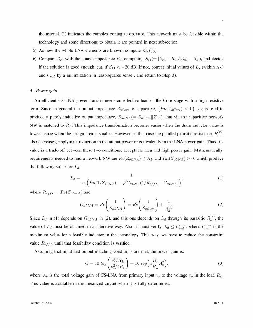
Fig. 4. (a) G and (b) NF for all-inversion regions and for four drain currents obtained applying the EOP without restrictions.
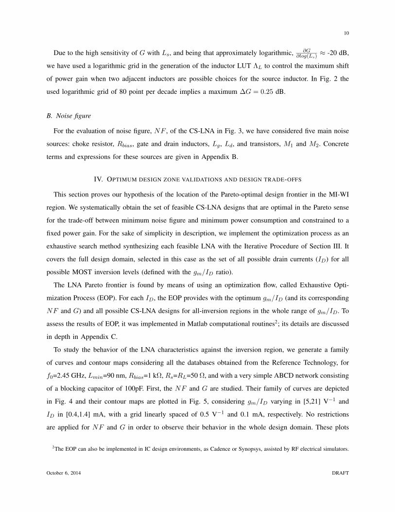
Fig. 5. Design space map of NF and G vs. ID and gm/ID without restrictions. Design points used in the methodology
validation as well as the Pareto optimal frontier (PF) are highlighted.
show the expected trade-off of NF and G versus current consumption: raising ID implies a reduction in
NF and an increment in G, and vice versa. Besides, when the gm/ID is swept, the best values of NF
and G are always obtained in MI , reaching a reduction of almost 1 dB in the NF and an improvement
of almost 10 dB in the G when compared with the figures of SI and WI; a feature not shown in prior
works.
October 6, 2014 DRAFT
Page 12
12
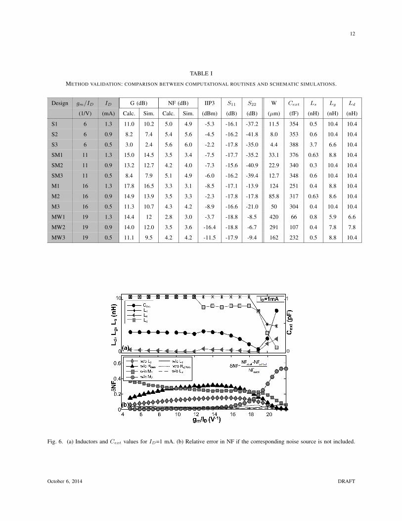
TABLE I
METHOD VALIDATION: COMPARISON BETWEEN COMPUTATIONAL ROUTINES AND SCHEMATIC SIMULATIONS.
Design gm/ID ID G (dB) NF (dB) IIP3 S11 S22 W Cext Ls Lg Ld
(1/V) (mA) Calc. Sim. Calc. Sim. (dBm) (dB) (dB) (µm) (fF) (nH) (nH) (nH)
S1 6 1.3 11.0 10.2 5.0 4.9 -5.3 -16.1 -37.2 11.5 354 0.5 10.4 10.4
S2 6 0.9 8.2 7.4 5.4 5.6 -4.5 -16.2 -41.8 8.0 353 0.6 10.4 10.4
S3 6 0.5 3.0 2.4 5.6 6.0 -2.2 -17.8 -35.0 4.4 388 3.7 6.6 10.4
SM1 11 1.3 15.0 14.5 3.5 3.4 -7.5 -17.7 -35.2 33.1 376 0.63 8.8 10.4
SM2 11 0.9 13.2 12.7 4.2 4.0 -7.3 -15.6 -40.9 22.9 340 0.3 10.4 10.4
SM3 11 0.5 8.4 7.9 5.1 4.9 -6.0 -16.2 -39.4 12.7 348 0.6 10.4 10.4
M1 16 1.3 17.8 16.5 3.3 3.1 -8.5 -17.1 -13.9 124 251 0.4 8.8 10.4
M2 16 0.9 14.9 13.9 3.5 3.3 -2.3 -17.8 -17.8 85.8 317 0.63 8.6 10.4
M3 16 0.5 11.3 10.7 4.3 4.2 -8.9 -16.6 -21.0 50 304 0.4 10.4 10.4
MW1 19 1.3 14.4 12 2.8 3.0 -3.7 -18.8 -8.5 420 66 0.8 5.9 6.6
MW2 19 0.9 14.0 12.0 3.5 3.6 -16.4 -18.8 -6.7 291 107 0.4 7.8 7.8
MW3 19 0.5 11.1 9.5 4.2 4.2 -11.5 -17.9 -9.4 162 232 0.5 8.8 10.4
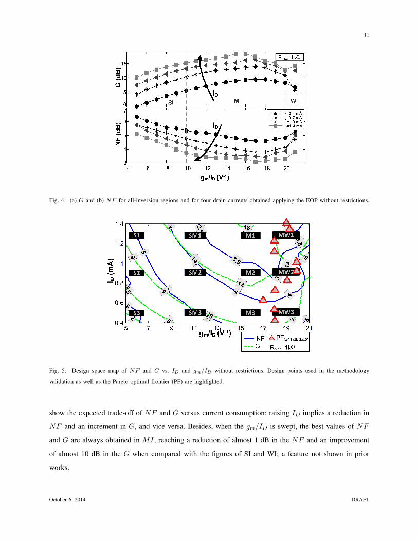
Fig. 6. (a) Inductors and Cext values for ID=1 mA. (b) Relative error in NF if the corresponding noise source is not included.
October 6, 2014 DRAFT
Page 13
13
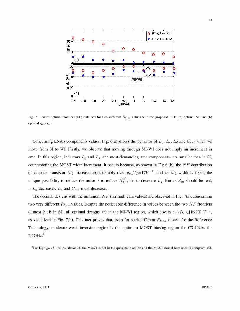
Fig. 7. Pareto optimal frontiers (PF) obtained for two different Rbias values with the proposed EOP: (a) optimal NF and (b)
optimal gm/ID .
Concerning LNA’s components values, Fig. 6(a) shows the behavior of Lg, Ls, Ld and Cext when we
move from SI to WI. Firstly, we observe that moving through MI-WI does not imply an increment in
area. In this region, inductors Lg and Ld -the most-demanding area components- are smaller than in SI,
counteracting the MOST width increment. It occurs because, as shown in Fig 6.(b), the NF contribution
of cascode transistor M2 increases considerably over gm/ID=17V −1, and as M2 width is fixed, the
unique possibility to reduce the noise is to reduce R(p)g , i.e. to decrease Lg. But as Zin should be real,
if Lg decreases, Ls and Cext must decrease.
The optimal designs with the minimum NF (for high gain values) are observed in Fig. 7(a), concerning
two very different Rbias values. Despite the noticeable difference in values between the two NF frontiers
(almost 2 dB in SI), all optimal designs are in the MI-WI region, which covers gm/ID ∈[16,20] V −1,
as visualized in Fig. 7(b). This fact proves that, even for such different Rbias values, for the Reference
Technology, moderate-weak inversion region is the optimum MOST biasing region for CS-LNAs for
2.4GHz.3
3For high gm/ID ratios, above 21, the MOST is not in the quasistatic region and the MOST model here used is compromised.
October 6, 2014 DRAFT
Page 14
14
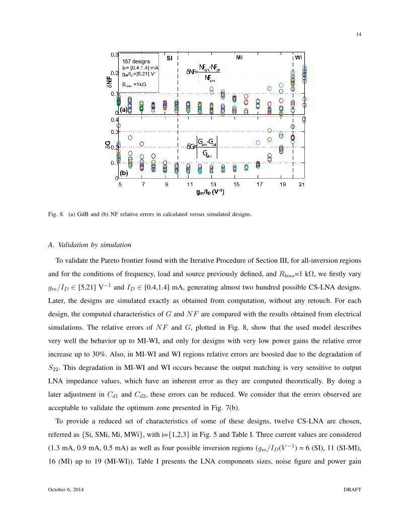
Fig. 8. (a) GdB and (b) NF relative errors in calculated versus simulated designs.
A. Validation by simulation
To validate the Pareto frontier found with the Iterative Procedure of Section III, for all-inversion regions
and for the conditions of frequency, load and source previously defined, and Rbias=1 kΩ, we firstly vary
gm/ID ∈ [5,21] V−1 and ID ∈ [0.4,1.4] mA, generating almost two hundred possible CS-LNA designs.
Later, the designs are simulated exactly as obtained from computation, without any retouch. For each
design, the computed characteristics of G and NF are compared with the results obtained from electrical
simulations. The relative errors of NF and G, plotted in Fig. 8, show that the used model describes
very well the behavior up to MI-WI, and only for designs with very low power gains the relative error
increase up to 30%. Also, in MI-WI and WI regions relative errors are boosted due to the degradation of
S22. This degradation in MI-WI and WI occurs because the output matching is very sensitive to output
LNA impedance values, which have an inherent error as they are computed theoretically. By doing a
later adjustment in Cd1 and Cd2, these errors can be reduced. We consider that the errors observed are
acceptable to validate the optimum zone presented in Fig. 7(b).
To provide a reduced set of characteristics of some of these designs, twelve CS-LNA are chosen,
referred as Si, SMi, Mi, MWi, with i=1,2,3 in Fig. 5 and Table I. Three current values are considered
(1.3 mA, 0.9 mA, 0.5 mA) as well as four possible inversion regions (gm/ID(V −1) = 6 (SI), 11 (SI-MI),
16 (MI) up to 19 (MI-WI)). Table I presents the LNA components sizes, noise figure and power gain
October 6, 2014 DRAFT
Page 15
15
obtained via the EOP with no constraints, for these twelve design points. Each LNA design is simulated
via SpectreRF, acquiring S11, S22, NF , G and IIP3.
B. Discussion
Figure 7, supported with the validation of Section IV.A, shows that LNA optimal designs are in the
MI/WI region. The use of all-inversion regions (SI, MI and WI) of the MOST is mandatory in this study
because only in this way the MI-WI region is proven as the optimum design zone.
Following the procedure of Section IV, the optimum design zone can be for other processes and other
LNA schemes [11], as the method only needs a small-signal modeling . This methodology also allows
the easy visualization of the design compromises, providing beforehand a complete panorama and insight
of the LNA behaviour when bias current and inversion level are modified.
The good results obtained in terms of noise figure or gain in all-inversion regions, particularly in
moderate and weak inversion are because of having considered the following effects in the CS-LNA
modeling: (1) simple semi-empirical MOST model covering all-inversion region; (2) noise parameters
modeled in MOST all-inversion regions; (3) inclusion of the effects of all components to compute
input/output impedance, in special all MOST capacitances; and (4) the inclusion of the cascode transistor
effects.
V. EXPERIMENTAL VALIDATION
The experimental validation of the optimum design zone is done by presenting an untrimmed 2.4-GHz
differential CS-LNA implemented in the Reference Technology to be used in a fully differential ZigBee
receiver. The results that will be shown are of the first integration of this stand-alone prototype. For
this implementation, the total power consumption and noise figure cannot surpass the 1.8 mW (with
VDD=1.2 V) and 5 dB respectively. The gain G must be higher than 10 dB and the IIP3 higher than
-5 dBm. The ABCD network is considered to be the blocking capacitor and the probing pad RF model.
Due to area constraints, Rbias is reduced up to 1 kΩ. This allows to place Rbias near M1 and reduce
considerably the layout parasitics in its MOST gate. Finally, to design a differential circuit based on the
proposed method, we obtain the single-ended design following the EOP of Section IV; then we mirror
the circuit to generate a differential structure. In our differential LNA we employ a differential symmetric
source inductor with its center tap connected to ground; since the Ls calculated by the procedure is single
ended, we use the double of this value to find a differential inductor included in the technology set. This
October 6, 2014 DRAFT
Page 16
16
TABLE II
COMPARISON BETWEEN MATLAB AND SPECTRERF SIMULATION
DATA FOR THE IMPLEMENTED CS-LNA AT 2.45 GHZ.
Characteristics Calculated Post-layout
(gm/ID, ID) (V −1, A) (17.4, 570µ)
Ls,Lg ,Ld (nH) 0.76, 8.8, 10.5 0.75, 11.1, 10.5
WM1(µm) 92.5 92
Cext (fF) 300 240
Cd1, Cd2 (pF) 0.38, 1.35 0.34, 0.53
G (dB) 12 10.3
NF (dB) 3.9 4.3
IIP3,P1dB,IIP2 (dBm) -7a, n/a,n/a -3.5,-15,61
S11,S22 (dB) -50,-21.5 -27,-15
a Obtained from electrical simulation
procedure was not done for Ld as the double of the computed values were not feasible in the Reference
Technology.
After running the EOP, the implemented design is chosen among all the ones included in the Pareto
frontier that have the minimum power consumption while achieving the above specifications. We consider
all those designs whose IIP3, estimated by electrical simulation of the schematic, are greater than a
bound of -7.5 dBm, near below the specified limit of -5 dBm to cover inaccuracies in the IIP3 computation.
The optimal designs that fulfill this requirement are the ones with ID >0.5 mA. Feature IIP3min is
only imposed to the post-layout representation due to its high sensitivity to gain variations. In addition,
as we need to consider those designs with power consumption restricted to 1.8 mW or less, a fine tuning
using a smaller grid of ID in the range of [0.5,0.8] mA is performed. The condition imposed is to
reduce as much as possible the power consumption while fulfilling the IIP3 requirement; the power
consumption of the final single-ended design is 684 µW. Table II lists the chosen design characteristics
as well as the post-layout simulations, which reach a good matching. Sizing adjustments of Lg and Cext
in the post-layout simulation are due to the compensation of layout parasitics of the routing and the pads
capacitances. The reduction in the final gain is because of the increment of parasitic resistances, which
in turn, increase the final IIP3.
Final schematic and the microphotograph of the implemented LNA are shown in Fig. 9; it covers
October 6, 2014 DRAFT
Page 17
17
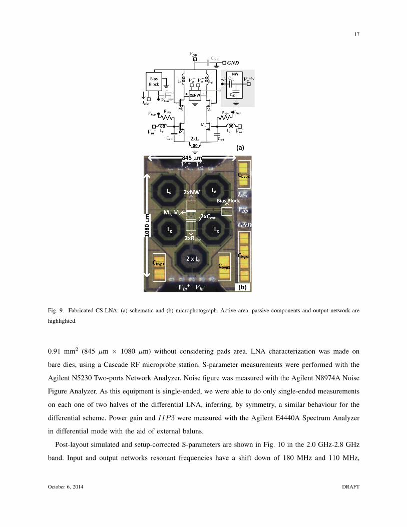
Fig. 9. Fabricated CS-LNA: (a) schematic and (b) microphotograph. Active area, passive components and output network are
highlighted.
0.91 mm2 (845 µm × 1080 µm) without considering pads area. LNA characterization was made on
bare dies, using a Cascade RF microprobe station. S-parameter measurements were performed with the
Agilent N5230 Two-ports Network Analyzer. Noise figure was measured with the Agilent N8974A Noise
Figure Analyzer. As this equipment is single-ended, we were able to do only single-ended measurements
on each one of two halves of the differential LNA, inferring, by symmetry, a similar behaviour for the
differential scheme. Power gain and IIP3 were measured with the Agilent E4440A Spectrum Analyzer
in differential mode with the aid of external baluns.
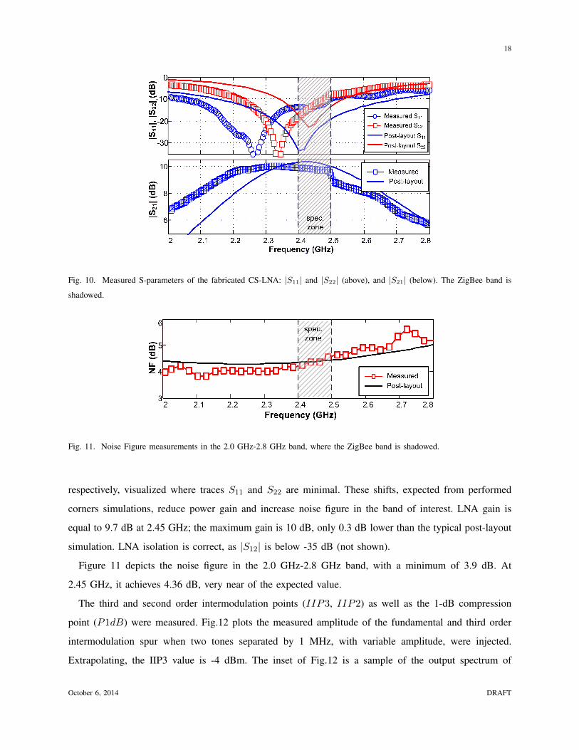
Post-layout simulated and setup-corrected S-parameters are shown in Fig. 10 in the 2.0 GHz-2.8 GHz
band. Input and output networks resonant frequencies have a shift down of 180 MHz and 110 MHz,
October 6, 2014 DRAFT
Page 18
18
Fig. 10. Measured S-parameters of the fabricated CS-LNA: |S11| and |S22| (above), and |S21| (below). The ZigBee band is
shadowed.
Fig. 11. Noise Figure measurements in the 2.0 GHz-2.8 GHz band, where the ZigBee band is shadowed.
respectively, visualized where traces S11 and S22 are minimal. These shifts, expected from performed
corners simulations, reduce power gain and increase noise figure in the band of interest. LNA gain is
equal to 9.7 dB at 2.45 GHz; the maximum gain is 10 dB, only 0.3 dB lower than the typical post-layout
simulation. LNA isolation is correct, as |S12| is below -35 dB (not shown).
Figure 11 depicts the noise figure in the 2.0 GHz-2.8 GHz band, with a minimum of 3.9 dB. At
2.45 GHz, it achieves 4.36 dB, very near of the expected value.
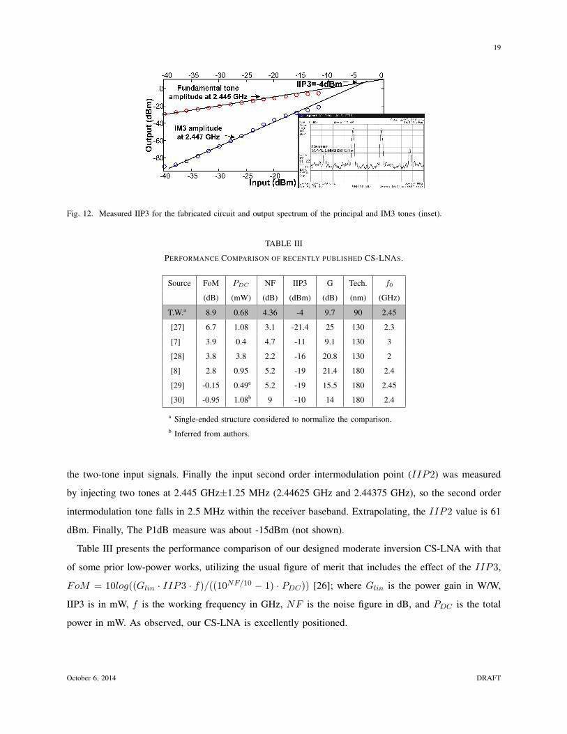
The third and second order intermodulation points (IIP3, IIP2) as well as the 1-dB compression
point (P1dB) were measured. Fig.12 plots the measured amplitude of the fundamental and third order
intermodulation spur when two tones separated by 1 MHz, with variable amplitude, were injected.
Extrapolating, the IIP3 value is -4 dBm. The inset of Fig.12 is a sample of the output spectrum of
October 6, 2014 DRAFT
Page 19
19
Fig. 12. Measured IIP3 for the fabricated circuit and output spectrum of the principal and IM3 tones (inset).
TABLE III
PERFORMANCE COMPARISON OF RECENTLY PUBLISHED CS-LNAS.
Source FoM PDC NF IIP3 G Tech. f0
(dB) (mW) (dB) (dBm) (dB) (nm) (GHz)
T.W.a 8.9 0.68 4.36 -4 9.7 90 2.45
[27] 6.7 1.08 3.1 -21.4 25 130 2.3
[7] 3.9 0.4 4.7 -11 9.1 130 3
[28] 3.8 3.8 2.2 -16 20.8 130 2
[8] 2.8 0.95 5.2 -19 21.4 180 2.4
[29] -0.15 0.49a 5.2 -19 15.5 180 2.45
[30] -0.95 1.08b 9 -10 14 180 2.4
a Single-ended structure considered to normalize the comparison.b Inferred from authors.
the two-tone input signals. Finally the input second order intermodulation point (IIP2) was measured
by injecting two tones at 2.445 GHz±1.25 MHz (2.44625 GHz and 2.44375 GHz), so the second order
intermodulation tone falls in 2.5 MHz within the receiver baseband. Extrapolating, the IIP2 value is 61
dBm. Finally, The P1dB measure was about -15dBm (not shown).
Table III presents the performance comparison of our designed moderate inversion CS-LNA with that
of some prior low-power works, utilizing the usual figure of merit that includes the effect of the IIP3,
FoM = 10log((Glin · IIP3 · f)/((10NF/10 − 1) · PDC)) [26]; where Glin is the power gain in W/W,
IIP3 is in mW, f is the working frequency in GHz, NF is the noise figure in dB, and PDC is the total
power in mW. As observed, our CS-LNA is excellently positioned.
October 6, 2014 DRAFT
Page 20
20
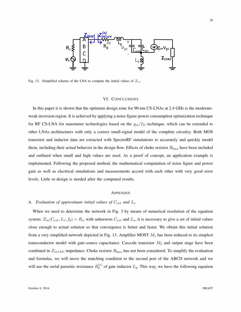
Fig. 13. Simplified scheme of the LNA to compute the initial values of Zin.
VI. CONCLUSIONS
In this paper it is shown that the optimum design zone for 90-nm CS-LNAs at 2.4 GHz is the moderate-
weak inversion region. It is achieved by applying a noise figure-power consumption optimization technique
for RF CS-LNA for nanometer technologies based on the gm/ID technique, which can be extended to
other LNAs architectures with only a correct small-signal model of the complete circuitry. Both MOS
transistor and inductor data are extracted with SpectreRF simulations to accurately and quickly model
them, including their actual behavior in the design flow. Effects of choke resistor Rbias have been included
and outlined when small and high values are used. As a proof of concept, an application example is
implemented. Following the proposed method, the mathematical computation of noise figure and power
gain as well as electrical simulations and measurements accord with each other with very good error
levels. Little re-design is needed after the computed results.
APPENDIX
A. Evaluation of approximate initial values of Cext and Ls
When we need to determine the network in Fig. 3 by means of numerical resolution of the equation
system: Zin(Cext, Ls; f0) = Rs, with unknowns Cext and Ls, it is necessary to give a set of initial values
close enough to actual solution so that convergence is better and faster. We obtain this initial solution
from a very simplified network depicted in Fig. 13. Amplifier MOST M1 has been reduced to its simplest
transconductor model with gate-source capacitance. Cascode transistor M2 and output stage have been
combined in ZLOAD impedance. Choke resistor Rbias has not been considered. To simplify the evaluation
and formulas, we will move the matching condition to the second port of the ABCD network and we
will use the serial parasitic resistance R(s)g of gate inductor Lg. This way, we have the following equation
October 6, 2014 DRAFT
Page 21
21
system:
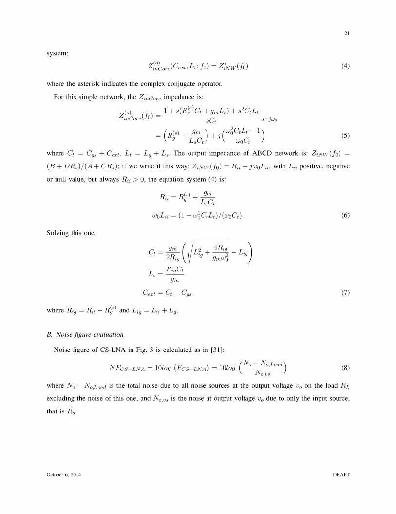
Z(o)inCore(Cext, Ls; f0) = Z∗iNW (f0) (4)
where the asterisk indicates the complex conjugate operator.
For this simple network, the ZinCore impedance is:
Z(o)inCore(f0) =
1 + s(R(s)g Ct + gmLs) + s2CtLt
sCt
∣∣s=jω0
=(R(s)g +
gmLsCt
)+ j(ω2
0CtLt − 1
ω0Ct
)(5)
where Ct = Cgs + Cext, Lt = Lg + Ls. The output impedance of ABCD network is: ZiNW (f0) =
(B +DRs)/(A+ CRs); if we write it this way: ZiNW (f0) = Rii + jω0Lii, with Lii positive, negative
or null value, but always Rii > 0, the equation system (4) is:
Rii = R(s)g +
gmLsCt
ω0Lii = (1− ω20CtLt)/(ω0Ct). (6)
Solving this one,
Ct =gm
2Rig
(√L2ig +
4Riggmω2
0
− Lig
)
Ls =RigCtgm
Cext = Ct − Cgs (7)
where Rig = Rii −R(s)g and Lig = Lii + Lg.
B. Noise figure evaluation
Noise figure of CS-LNA in Fig. 3 is calculated as in [31]:
NFCS−LNA = 10log(FCS−LNA
)= 10log
(No −No,Load
No,vs
)(8)
where No −No,Load is the total noise due to all noise sources at the output voltage vo on the load RL
excluding the noise of this one, and No,vs is the noise at output voltage vo due to only the input source,
that is Rs.
October 6, 2014 DRAFT
Page 22
22
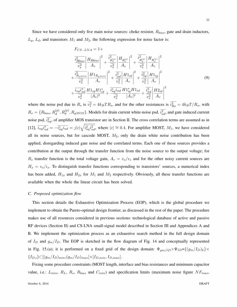
Since we have considered only five main noise sources: choke resistor, Rbias, gate and drain inductors,
Lg, Ld, and transistors M1 and M2, the following expression for noise factor is:
FCS−LNA = 1+
i2Rbiasv2s
∣∣∣∣∣HRbias
Av
∣∣∣∣∣2
+i2R
(p)g
v2s
∣∣∣∣∣HR(p)g
Av
∣∣∣∣∣2
+i2R
(p)d
v2s
∣∣∣∣∣HR(p)d
Av
∣∣∣∣∣2
+i2RgMOS
v2s
∣∣∣∣∣H1RgMOS
Av
∣∣∣∣∣2
+i2ndv2s
∣∣∣∣∣H1idAv
∣∣∣∣∣2
+i2ng
v2s
∣∣∣∣∣H1igAv
∣∣∣∣∣2
(9)
+ingi∗ndv2s
H1igH1∗id|Av|2
+i∗ngind
v2s
H1∗igH1id
|Av|2+i2ndv2s
∣∣∣∣∣H2idAv
∣∣∣∣∣2
where the noise psd due to Rs is v2s = 4kBTRs, and for the other resistances is i2Rx = 4kBT/Rx, with
Rx = Rbias, R(p)d , R
(p)g , RgMOS. Models for drain current white-noise psd, i2nd, and gate induced current
noise psd, i2ng, of amplifier MOS transistor are in Section II. The cross correlation terms are assumed as in
[12], ingi∗nd = −i∗ngind = j|c|√i2ngi
2nd, where |c| ∼= 0.4. For amplifier MOST, M1, we have considered
all its noise sources, but for cascode MOST, M2, only the drain white noise contribution has been
applied, disregarding induced gate noise and the correlated terms. Each one of these sources provides a
contribution at the output through the transfer function from the noise source to the output voltage; for
Rs transfer function is the total voltage gain, Av = vo/vs and for the other noisy current sources are
Hx = vo/ix. To distinguish transfer functions corresponding to transistors’ sources, a numerical index
has been added, H1x and H2x for M1 and M2 respectively. Obviously, all these transfer functions are
available when the whole the linear circuit has been solved.
C. Proposed optimization flow
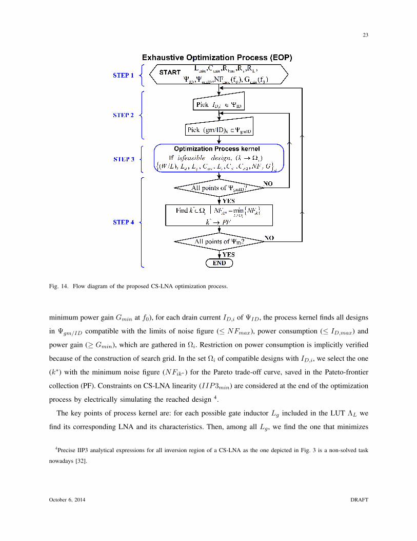
This section details the Exhaustive Optimization Process (EOP), which is the global procedure we
implement to obtain the Pareto-optimal design frontier, as discussed in the rest of the paper. The procedure
makes use of all resources considered in previous sections: technological database of active and passive
RF devices (Section II) and CS-LNA small-signal model described in Section III and Appendices A and
B. We implement the optimization process as an exhaustive search method in the full design domain
of ID and gm/ID. The EOP is sketched in the flow diagram of Fig. 14 and conceptually represented
in Fig. 15.(a); it is performed on a fixed grid of the design domain: Ψgm/ID×ΨID=(gm/ID)k×
ID,i⊂[(gm/ID)min,(gm/ID)max]×[ID,min, ID,max].
Fixing some procedure constraints (MOST length, interface and bias resistances and minimum capacitor
value, i.e.: Lmin, RL, Rs, Rbias and Cmin) and specification limits (maximum noise figure NFmax,
October 6, 2014 DRAFT
Page 23
23
Fig. 14. Flow diagram of the proposed CS-LNA optimization process.
minimum power gain Gmin at f0), for each drain current ID,i of ΨID, the process kernel finds all designs
in Ψgm/ID compatible with the limits of noise figure (≤ NFmax), power consumption (≤ ID,max) and
power gain (≥ Gmin), which are gathered in Ωi. Restriction on power consumption is implicitly verified
because of the construction of search grid. In the set Ωi of compatible designs with ID,i, we select the one
(k∗) with the minimum noise figure (NFik∗) for the Pareto trade-off curve, saved in the Pateto-frontier
collection (PF). Constraints on CS-LNA linearity (IIP3min) are considered at the end of the optimization
process by electrically simulating the reached design 4.
The key points of process kernel are: for each possible gate inductor Lg included in the LUT ΛL we
find its corresponding LNA and its characteristics. Then, among all Lg, we find the one that minimizes
4Precise IIP3 analytical expressions for all inversion region of a CS-LNA as the one depicted in Fig. 3 is a non-solved task
nowadays [32].
October 6, 2014 DRAFT
Page 24
24
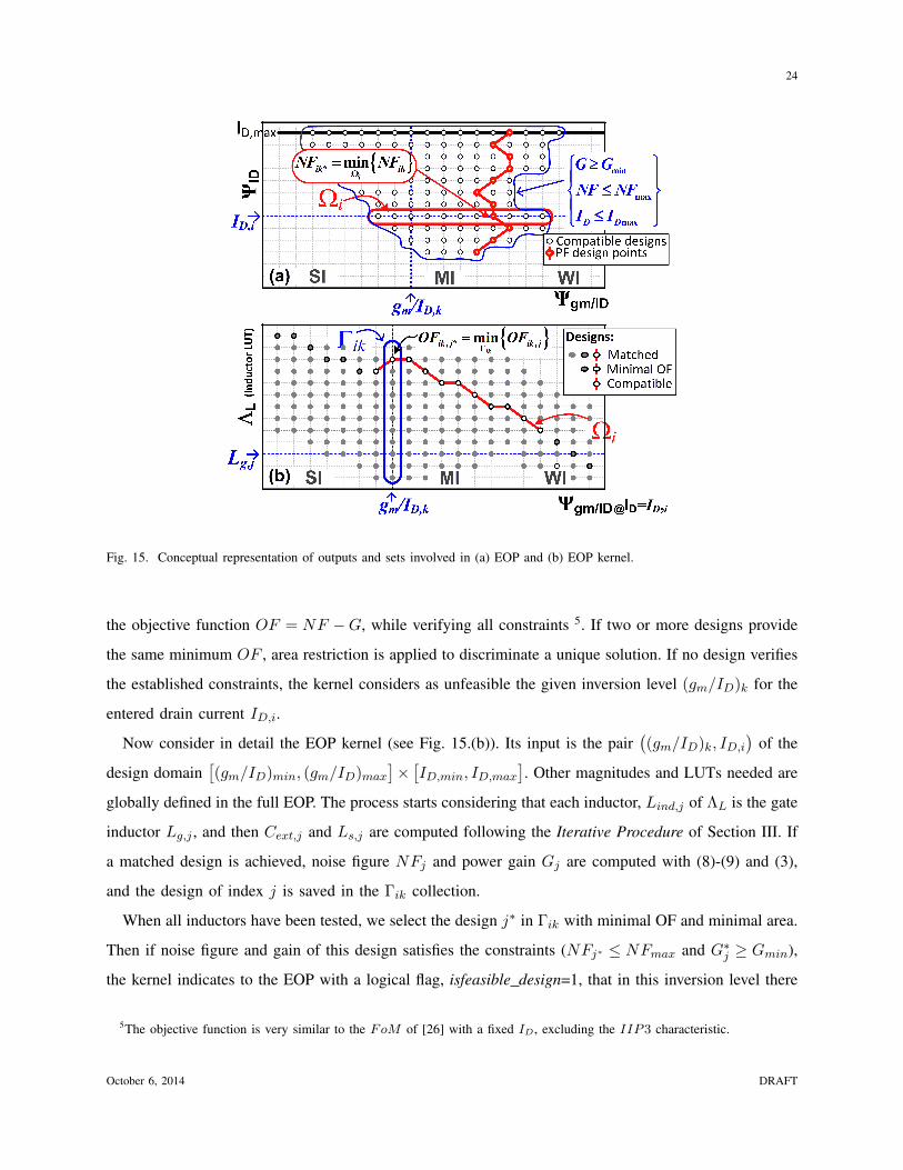
Fig. 15. Conceptual representation of outputs and sets involved in (a) EOP and (b) EOP kernel.
the objective function OF = NF −G, while verifying all constraints 5. If two or more designs provide
the same minimum OF , area restriction is applied to discriminate a unique solution. If no design verifies
the established constraints, the kernel considers as unfeasible the given inversion level (gm/ID)k for the
entered drain current ID,i.
Now consider in detail the EOP kernel (see Fig. 15.(b)). Its input is the pair((gm/ID)k, ID,i
)of the
design domain[(gm/ID)min, (gm/ID)max
]×[ID,min, ID,max
]. Other magnitudes and LUTs needed are
globally defined in the full EOP. The process starts considering that each inductor, Lind,j of ΛL is the gate
inductor Lg,j , and then Cext,j and Ls,j are computed following the Iterative Procedure of Section III. If
a matched design is achieved, noise figure NFj and power gain Gj are computed with (8)-(9) and (3),
and the design of index j is saved in the Γik collection.
When all inductors have been tested, we select the design j∗ in Γik with minimal OF and minimal area.
Then if noise figure and gain of this design satisfies the constraints (NFj∗ ≤ NFmax and G∗j ≥ Gmin),
the kernel indicates to the EOP with a logical flag, isfeasible design=1, that in this inversion level there
5The objective function is very similar to the FoM of [26] with a fixed ID , excluding the IIP3 characteristic.
October 6, 2014 DRAFT
Page 25
25
is a compatible design, and the kernel outputs this design too.
REFERENCES
[1] D. Comer and D. Comer, “Operation of analog MOS circuits in the weak or moderate inversion region,” IEEE Transactions
on Education, vol. 47, no. 4, pp. 430–435, 2004.
[2] A.-S. Porret and et al., “An ultralow -power UHF transceiver integrated in a standard digital CMOS process: Arquitecture
and receiver,” IEEE Journal of Solid-State Circuits, vol. 36, no. 3, pp. 452–464, Mar. 2001.
[3] J. Ramos and et al, “90nm RF CMOS technology for low-power 900MHz applications,” Proceeding of the 34th European
Solid-State Device Research conference ESSDERC 2004, pp. 329–332, Sep. 2004.
[4] L. Barboni, R. Fiorelli, and F. Silveira, “A tool for design exploration and power optimization of CMOS RF circuit blocks,”
IEEE International Symposium on Circuits and Systems ISCAS’06, May 2006.
[5] A. Shameli and P. Heydari, “A novel power optimization technique for ultra-low power RFIDs,” in International Symposium
on Low Power Electronics and Design, G. Tegernsee, Ed., 2006.
[6] H. Lee and S. Mohammadi, “A subthreshold low phase noise CMOS LC VCO for ultra low power applications,” IEEE
Microwave and Wireless Component Letters, vol. 17, no. 11, pp. 796–799, Nov. 2007.
[7] ——, “A 3GHz subthreshold CMOS low noise amplifier,” in Proc. IEEE Radio Frequency Integrated Circuits (RFIC)
Symp, 2006.
[8] A. V. Do, C. C. Boon, M. A. Do, K. S. Yeo, and A. Cabuk, “A subthreshold low-noise amplifier optimized for ultra-
low-power applications in the ISM band,” IEEE Transactions on Microwave Theory and Techniques, vol. 56, no. 2, pp.
286–292, 2008.
[9] H.-S. Jhon and et al, “0.7 V supply highly linear subthreshold low-noise amplifier design for 2.4GHz wireless sensor
network applications,” Microwave And Optical Technology Letters, vol. 51, no. 5, pp. 1316–1320, May 2009.
[10] R. Fiorelli, E. Peralıas, and F. Silveira, “LC-VCO design optimization methodology based on the gm/ID ratio for nanometer
CMOS technologies,” IEEE Transactions on Microwave Theory and Techniques, vol. 59, no. 7, pp. 1822–1831, Jul. 2011.
[11] R. Fiorelli and F. Silveira, “Common gate LNA design space exploration in all inversion regions,” in Argentine School of
Micro-Nanoelectronics, Technology and Applications, EAMTA., 2008, pp. 119–122.
[12] D. Shaeffer and T. H. Lee, “A 1.5-V, 1.5-GHz CMOS low noise amplifier,” IEEE Journal of Solid-State Circuits, vol. 32,
no. 5, pp. 745–759, May 1997.
[13] T.-K. Nguyen, C.-H. Kim, G.-J. Ihm, M.-S. Yang, , and S.-G. Lee, “CMOS low-noise amplifier design optimization
techniques,” IEEE Transactions on Microwave Theory and Techniques, vol. 52, no. 5, pp. 1433–1442, May 2004.
[14] L. Belostotski and J. W. Haslett, “Noise figure optimization of inductively degenerated CMOS LNAs with integrated gate
inductors,” IEEE Transactions on Circuits and Systems, vol. 53, no. 7, pp. 1409–1422, Jul 2006.
[15] P. Andreani and H. Sjoland, “Noise optimization of an inductively degenerated CMOS low noise amplifier,” IEEE
Transactions on Circuits and Systems, vol. 48, no. 9, pp. 835–841, Sept 2001.
[16] J. Janssens and M. Steyaert, CMOS Celular Receiver Front-ends. Kluwer Academic Publishers, 2002.
[17] G. Tulunay and S. Balkir, “A synthesis tool for CMOS RF low-noise amplifiers,” IEEE Transactions on Computer-Aided
Design of Integrated Circuits and Systems, vol. 27, no. 5, pp. 977–982, 2008.
[18] A. Nieuwoudt, T. Ragheb, H. Nejati, and Y. Massoud, “Numerical design optimization methodology for wideband and
multi-band inductively degenerated cascode CMOS Low Noise Amplifiers,” IEEE Transactions on Circuits and Systems I,
vol. 56, no. 6, pp. 1088–1101, 2009.
October 6, 2014 DRAFT
Page 26
26
[19] N. Barabino, R. Fiorelli, and F. Silveira, “Efficiency based fesign for fully-integrated Class C RF Power Amplifiers in
nanometric CMOS,” in Proceedings of IEEE International Symposium in Circuits and Systems, ISCAS 2010, May 2010.
[20] Z. Deng and A. M. Niknejad, “On the noise optimization of CMOS common-source low-noise amplifiers,” IEEE
Transactions on Circuits and Systems—Part I: Fundamental Theory and Applications, vol. 58, no. 4, pp. 654–667, 2011.
[21] F. Silveira, D. Flandre, and P. G. A. Jespers, “A gm/ID based methodology for the design of CMOS analog circuits and
its applications to the synthesis of a silicon-on-insulator micropower OTA,” IEEE Journal of Solid-State Circuits, vol. 31,
no. 9, pp. 1314–1319, Sep. 1996.
[22] P. G. Jespers, The gm/ID Methodology, a sizing tool for low-voltage analog CMOS Circuits. Springer, 2010.
[23] A.Cunha, M. C. Schneider, and C. Galup-Montoro, “An MOS transistor model for analog circuit design,” IEEE Journal
of Solid-State Circuits, vol. 33, no. 10, pp. 1510–1519, Oct. 1998.
[24] Y. Tsividis, Operation and Modelling of the MOS Transistor, 2nd ed. Oxford University Press, 2000.
[25] R. Fiorelli, F. Silveira, A. Rueda, and E. Peralıas, “Semi-empirical model of MOST and passive devices focused on
narrowband RF blocks,” in XXVII Conference on Design of Circuits and Integrated Systems (DCIS), Nov. 2012.
[26] R. Brederlow, W. Weber, J. Sauerer, S. Donnay, P. Wambacq, and M. Vertregt, “A mixed-signal design roadmap,” IEEE
Design Test of Computers, vol. 18, no. 6, pp. 34 –46, nov/dec 2001.
[27] F. Tzeng, A. Jahanian, and P. Heydari, “A multiband inductor-reuse CMOS low-noise amplifier,” IEEE Transactions on
Circuits and Systems II, vol. 55, no. 3, pp. 209–213, 2008.
[28] J. Borremans, P. Wambacq, C. Soens, Y. Rolain, and M. Kuijk, “Low-area active-feedback low-noise amplifier design in
scaled digital CMOS,” IEEE Journal of Solid-State Circuits, vol. 43, no. 11, pp. 2422 –2433, Nov. 2008.
[29] T. Tran, C. Boon, M. Do, and K. Yeo, “Ultra-low power series input resonance differential common gate LNA,” Electronics
Letters, vol. 47, no. 12, pp. 703 –704, Sep. 2011.
[30] A. V. Do, C. C. Boon, M. A. Do, K. S. Yeo, and A. Cabuk, “An energy-aware CMOS receiver front end for low-power
2.4-GHz applications,” IEEE Transactions on Circuits and Systems I, vol. 57, no. 10, pp. 2675–2684, 2010.
[31] B. Razavi, RF Microelectronics. Prentice Hall Inc., 1998.
[32] B. Toole, C. Plett, and M. Cloutier, “RF circuit implications of moderate inversion enhanced linear region in MOSFETs,”
IEEE Transactions on Circuits and Systems I, vol. 51, no. 2, pp. 319 – 328, Feb. 2004.
October 6, 2014 DRAFT