Introduction, 1Defining Properties of Solids, 1Fundamental Nature of Electrical Conductivity, 4Temperature Dependence of Electrical Conductivity, 4Essential Elements of Quantum Mechanics, 7Quantum Numbers, 13Pauli Exclusion Principle, 14Periodic Table of Elements, 15Some Important Concepts of Solid-State Physics, 18Signature Properties of Superconductors, 19Fermi–Dirac Distribution Function, 24Band Structure of Solids, 27
Do not worry about your difficulties in Mathemat-ics, I can assure you mine are still greater.
Albert Einstein
1.1 Introduction
In this chapter, we will learn about the fundamentalnature of solids and how their defining propertiesare associated with quantum mechanical concepts ofelectrons and their energy. The exposure to the mostessential concepts of solid-state physics will greatlyhelp us in understanding the nature of electroceramicsand the multiple physical phenomena they can exhibitthat form the basis for a large number of novel deviceapplications that impact electronic and sensor technol-ogy. We have purposely tried to avoid the intricaciesof mathematical models in describing these conceptsbecause the goal here is not to produce another book onsolid-state physics but rather to make use of the essentialfeatures of various theoretical models in understand-ing the transport properties of electrons, uniquenessof semiconductors, and the scientific basis behind thedielectric properties of materials.
1.2 Defining Properties of Solids
Solids can be broadly classified as conductors, semicon-ductors, and insulators of which dielectrics are a subset.Another important group of solids are classified as hightemperature superconductors. Because of the uniquephysical mechanisms involved in the origin of supercon-ductivity, these materials are of a special category andwill be treated as an independent class of materials. Wewill devote a section on superconductivity later in thischapter. So far as the other three groups are concerned,we can differentiate between them on the basis of theirdefining properties. For example, a conductor is definedby its capacity to facilitate the transport of an electricalcurrent associated with the inherent material propertythat we call resistance. Similarly a semiconductor isdefined by its energy gap (also, called bandgap) and adielectric by its dielectric property. We discuss in thischapter, the origin of these properties and how they adduniqueness to materials.
1.2.1 Electrical Conductance (G)
All materials tend to resist the flow of an electric currentby virtue of its built-in resistance. The magnitude
of current, I, is dictated by the resistance, R (or,conductance, G) when a voltage, V , is applied betweenthe two ends of a solid sample. This relationship isgiven by the famous law of physics universally knownas the Ohm’s law that was conceived in 1825–1826 byGerog Ohm of Germany. It states that the current (I)generated between the two fixed points of a conductor(such as a metal) is directly proportional to the potentialapplied and inversely proportional to its resistance.Mathematically, it is expressed as Eq. (1.1).
I = VR
= GV (1.1)
Here G being the conductance that is simply the inverseof resistance. From the above equation, we can concludethat I increases as R decreases or it increases with theincrease in conductivity G. The resistance (R) changesas two reference points between which it is measured ischanged. For example, it increases with the increase inthe distance between the reference points and decreasesif the distance between these points is reduced. Thatmeans that the resistance (or, conductance) is dependentupon the geometry of the sample. In other words, neitherresistance nor conductance is the intrinsic property ofthe sample under consideration. Unless we can developthe concept of intrinsic resistance of a material, wewould not be able develop theoretical models that areindependent of sample geometry. To accomplish thisgoal, let us introduce now a parameter which we shallcall resistivity. It is defined as follows:
𝜌 = R(A
L
)(1.2)
Here 𝜌 is the resistivity, L the sample length, and A thecross-sectional area. The unit of the resistivity is Ω m.We can see from the above equation that the resistivitybecomes an intrinsic property of materials. No two mate-rials would have the same value of resistivity.
While defining the resistivity, we assumed the sampleto be uniform in which the current flows uniformly.However, in reality that may not always be the case. Wetherefore need to develop a more basic definition ofresistivity. We can imagine that an electric field prevailsinside the sample when it experiences a potential dif-ference between any two fixed points. It is actually theelectric field (E) that enables the current flow within thesample, and therefore, the resistivity must be associatedwith the current density (J) that exists within the sample.We can then redefine the resistivity with respect to Eand J as in Eq. (1.3).
𝜌 =(V
L
)⋅(A
I
)= E
J(1.3)
The inverse of the resistivity is called conductivity (𝜎)and its unit is S m−1 or (Ω m)−1. Replacing the resistivity
with conductivity, we can rewrite Eq. (1.3) in its alterna-tive formulation as follows:
J = 𝜎E (1.4)
Metals have the highest conductivity among all solids,and it is greater than 105 (S m−1). In comparison, in semi-conductors, it varies from 10−6 <𝜎 < 105 (S m−1). Thedielectrics have very small conductivity that is smallerthan 10−6 (S m−1). Based on this information, we cannow distinguish between the three types of solids as inEq. (1.5).
𝜎metal ≫ 𝜎semiconductor ≫ 𝜎dielectric (1.5)
In Table 1.1, a list of materials with their electrical con-ductivity is presented.
1.2.2 Bandgap, Eg
The defining property of a semiconductor is its energybandgap that exists between the valence band and theconduction band. The width of the bandgap is expressedin electron volt with the symbol of Eg. The unit ofelectron volts for energy is defined as the work donein accelerating an electron through 1 V of potentialdifference. For converting 1 J of energy to electron volts,we need to divide it by the charge of an electron that is1.602× 10−19 C.
The concept of energy being in bands of solids insteadof just being discrete is based on the band theory ofsolids to which we will introduce our readers later inthis chapter. For the time being, let us be satisfied withthe assumption that electrons and other charge carriers(e.g. holes) can reside only in the valence band or theconduction band. It is forbidden for any charge car-rier to be found in the bandgap at absolute zero. TheFermi–Dirac distribution function (also known as F-D
Table 1.1 Room temperature electrical conductivity of selectedsolids.
Materials Electrical conductivity, 𝝈 (S m−1)
Aluminum (Al) 3.5× 10⁷
Carbon (graphene) 1.00× 10⁸
Carbon (diamond) ≈10−13
Copper (Cu) 5.96× 10⁷
Gold (Au) 4.10× 10⁷
Silver (Ag) 6.30× 10⁷
Platinum (Pt) 9.43× 10⁶
Germanium (Ge) 2.17 (depends on doping)Silicon (Si) 1.56× 10⁻³ (depends on doping)Gallium arsenide (GaAs) 1.00× 10⁻⁸ to 103
Nature and Types of Solid Materials 3
statistics) with its enormous importance to the quantumnature of solids completely excludes the possibility thatany electron can be found in the bandgap. Not only that,this theory also predicts that at absolute zero (0 K), allelectrons are frozen in valence band, and the conductionband is completely empty. We will deal also with thismagnificent theory later in this chapter. However, it isalso probable that some electrons might get sufficientkinetic energy to escape the valence band and migrate tothe conduction band. But this probability is allowed onlyat temperature ≫0 K according to the F-D statistics.
In general, metals have almost no bandgap, whereasinsulators have large bandgaps. The bandgaps of semi-conductors lie between these two extremes. If thebandgap is greater than 2 eV, the material is thoughtto be an insulator, though this notion is not alwayssupported by facts. For example, there are many semi-conductors with Eg > 2 eV, and they are classified as widebandgap semiconductors and not insulators.
The semiconductors are normally classified as nar-row bandgap, midlevel bandgap, and wide bandgap.In Figure 1.1, a qualitative picture of bandgap is given,which can serve for distinguishing among metals,semiconductors, and dielectrics.
We see in Figure 1.1 that dielectrics have much largerbandgaps than semiconductors, whereas metals have nobandgap at all. In fact, the two bands merge in metalscausing an overlapped region, where electrons are sharedby the two bands. We also find in this figure that besidesthe bandgap, there is another parameter labeled as Fermilevel, which lies between the upper (conduction band)and lower (valence band) energy bands. It is defined asthe sum of the potential energy and kinetic energy. Forconvenience, for example, in discussing the semiconduc-tor properties, the potential energy is set at zero corre-sponding to the bottom of the valence band.
It is important to know that all solids have Fermienergy, and its location with respect to the bandgap
is commonly referred to as Fermi level. We can nowsummarize that
Eg,dielectric ≫ Eg,semiconductor ≫ Eg,metal (1.6)
In Table 1.2, values for the bandgap for some commonsemiconductor materials is given at 300 K.
1.2.3 Permeability, 𝝐
From Figure 1.1, we can also conclude based on the argu-ments advanced in the previous section that the largebandgap of a dielectric material would inhibit the elec-trical conduction since it would be difficult for electronsto gain sufficient energy to overcome the bandgap atroom temperature. This is certainly consistent withour everyday experience that dielectrics are very poorcarriers of electricity. However, one need to rememberthat theoretically even the best of dielectric can conductelectricity when subjected to a large potential difference,but the magnitude of the resulting current would be sosmall as to be of any practical interest.
The defining property of a dielectric material is thepermittivity, which is also known by its other name ofdielectric constant with the universal symbol of 𝜖. Allmaterials will get polarized when subjected to an electric
Table 1.2 Some semiconductor materials and their bandgap.
Materials Bandgap (eV)
Ge 0.661Si 1.12InSb 0.17InP 1.344GaAs 1.424
Source: From http://hyperphysics.phy-astr.gsu.edu/hbase/hph.html.
Fermi level Bandgap, Eg (eV) Eg
Conduction band (CB)
Conduction band (CB)
Conduction band (CB)
Valence band (VB) Valence band (VB)
Ene
rgy
Valence band (VB)
Overlap
Dielectric Semiconductor Metal
Figure 1.1 Comparative representation of insulators, semiconductors, and metals on the basis of their energy bandgaps.
4 Fundamentals of Electroceramics
field. We know that the relationship between the electricdisplacement (D), and the electric field (E) is given by thefundamental equation of electromagnetics which statesthat
D = 𝜖0E + P (1.7)
where 𝜖0 is the permittivity of vacuum with the value of8.85× 10−12 F m−1 and P the electric field-induced polar-ization. At low electric field, the product 𝜖0E is a verysmall number, and therefore, we can approximate D≈P.Therefore, for low electric fields, Eq. (1.7) takes the formof Eq. (1.8).
P ≈ 𝜖r𝜖0E (1.8)
The parameter 𝜖r is the relative dielectric constant thatis a unitless quantity and is equal to 𝜖 ⋅ 𝜖−1
0 , where 𝜖 isthe permittivity of the material. The permittivity is spe-cific to a material similar to the electrical conductivity.Therefore, we can also use this parameter to distinguishbetween the three types of solids as shown in the rela-tionship in Eq. (1.9).
𝜖r,dielectric ≫ 𝜖r,semiconductor ≫ 𝜖r,metal (1.9)
In Table 1.3, a list of relative dielectric constant (𝜖r) forselected materials is presented.
1.3 Fundamental Nature of ElectricalConductivity
We defined in Eq. (1.4) the electric current, I. This deriva-tion was based on geometrical considerations of a sampleof finite size and length. The question now arises whatcauses the onset of current and how do we understand itstrue nature. To accomplish this goal, we need to considerthat the current is generated when electrons move fromone point to another under the influence of an appliedelectric field. Such a movement will obviously involve avelocity and mobility.
Table 1.3 Dielectric constant of some selected materials.
Source: From http://hyperphysics.phy-astr.gsu.edu/hbase/hph.html.
We can easily visualize a picture in which a travelingelectron will encounter thermally generated phonons ina crystal lattice and then will acquire an average velocitythat is also called the drift velocity, vd. But what arephonons and where do they come from? It is quantummechanical concept and refers to the unit of vibrationalenergy originating from the oscillations of atoms withina crystal lattice. The atomic oscillations increase withincreasing temperature resulting in larger number ofthermally generated phonons. Phonons are the coun-terpart of photons and both being quantum mechanicalconcepts. They are the two main types of elementaryparticles associated with solids.
The magnitude of the drift velocity will be propor-tional to the applied electric field. The coefficient ofproportionality is called the electron mobility (𝜇e).Alternatively, it can also be defined with the help of thefollowing equation:
𝜇e =(Δvd
ΔE
)(1.10)
The electron mobility is a very important property andplays a vital role in designing a transistor. Materials withlarger values of mobility are desired because that trans-lates to faster transistors. We will discuss this parameteragain in Chapter 7. Its unit is m2 V−1 s−1.
We can easily visualize that electrical conductivity (𝜎e)and electron mobility (𝜇e) to be related somehow. Wecan in fact find this relationship simply by assuming thatthere are n number of electrons involved and their trans-port from one point to another is facilitated by the onsetof mobility (𝜇e) and the applied electric field (E) such that
𝜎e = ne𝜇e (1.11)
where e is obviously the electronic charge. Equation (1.11)is the standard expression and gains a special importancewhile dealing with semiconductor materials where theconductivity is the sum of the contributions made byelectrons and holes. This is discussed also in Chapter 7.
1.4 Temperature Dependenceof Electrical Conductivity
Resistivity of solids is highly temperature-dependent.Strong thermal dependence of resistivity is exhibited bymetals and semiconductors. However, their trends areopposite to each other. They are displayed in Figure 1.2.We can see here that metal resistivity first remains con-stant in the low temperature regime until a temperatureis reached above which it starts increasing rapidly as thetemperature increases. At high temperature regime, itfollows approximately a linear relationship with tem-perature yielding a positive temperature coefficient of
Nature and Types of Solid Materials 5
resistivity(
Δ𝜌ΔT
= 𝜂)
. The semiconductor resistivity, onthe other hand, increases rapidly with decreasing tem-perature following an exponential thermal dependence.At sufficiently low temperatures, all semiconductorsbecome good insulators. At higher temperatures, itsresistivity decreases at a vastly reduced rate such thatthe change is almost monotonous. Resistivity of atypical insulator follows qualitatively the same temper-ature dependence as semiconductors. Obviously, theresistivity of an insulator is much greater than that ofsemiconductors as can be concluded from Figure 1.1.
In Figure 1.2, we have included the temperature depen-dence of resistivity also for a superconductor simply todemonstrate the distinction one can make between met-als, semiconductors, and superconductors based on thebehavior of their electrical resistivity with temperature.In superconductors, the resistivity goes through a phasechange at a critical temperature, called the superconduct-ing transition point below which a normal metal becomessuperconducting. Its resistance vanishes and the materialacquires infinite conductivity and remains in the super-conducting state so long as temperature remains belowthe transition point. Above the critical temperature, itloses its superconducting nature and behaves like a nor-mal metal. The thermal behavior of solids, as shown inFigure 1.2, can be easily explained on the basis of physicsas describe below.
1.4.1 Case of Metals
The thermal behavior of electrical resistivity of metalscan be expressed empirically by Matthiessen’s rule that
Superconductor
Metal
Temperature, T
Residual resistivity, ρ0
Resis
tivity, ρ
Semiconductor(also semi-insulators)
Superc
onductin
gtra
nsitio
n p
oin
t
ρ0
Figure 1.2 Temperature dependence of resistivity of metals,semiconductors, and superconductors.
is given by Eq. (1.12).
𝜌net = 𝜌0 + 𝜌(T) (1.12)
where 𝜌0 the temperature-independent part and𝜌(T) the temperature-dependent part. The origin oftemperature-independent part of the resistivity lies inthe presence of impurities and imperfections in thesample. It dominates at low temperatures followingthe 𝜌0 ∝T5 law. Below a certain temperature called,the Debye temperature, it remains constant. Above theDebye temperature, the resistivity increases linearlywith temperature obeying the 𝜌≈ 𝜂T relationship. Thetemperature-dependent part is due to the thermal vibra-tions of the lattice. At high temperatures, more and morephonons are excited impacting the thermal behavior ofresistivity. The knowledge of the thermal dependenceof metal resistivity above room temperature gives usthe value of the temperature coefficient, 𝜂, which hasimportant practical applications in temperature mea-suring devices such as thermocouples and thermistors.We can easily determine its value by measuring theresistance at some well-defined temperatures. Let us saythat at temperature T0, the resistance is R0, and it is Rat temperature T , which is greater than temperature T0.Then 𝜂 can be expressed as in Eq. (1.13) (Table 1.4).
𝜂 =(R − R0)
R (T − T0)=(ΔRΔT
)⋅
1R
(1.13)
1.4.2 Case of Semiconductors
For intrinsic semiconductor, the conduction can onlytake place when electrons closest to the surface of thebandgap acquire sufficient energy to escape the bandgapand reach the conduction band. The temperaturedependence of the resistivity (𝜌) is given by Eq.(1.14).
𝜌 = 𝜌0 exp(−
Eg
2kBT
)(1.14)
Table 1.4 Temperature coefficient of resistivity (𝜂) of somecommon metals.
Metals 𝜼 × 10−3 (per ∘C)
Silver, Ag 3.8Copper, Cu 3.9Gold, Au 3.4Aluminum, Al 4.3Iron, Fe 6.5Tungsten, W 4.5Platinum, Pt 3.92
Nichrome is an alloy of Ni and Cr.Source: From http://hyperphysics.phy-astr.gsu.edu/hbase/hph.html.
6 Fundamentals of Electroceramics
Perm
ittivity
Dipolarpolarization
UHF-MW MW-IRFrequency
Imaginary part, ε″
Ionicpolarization
Electronic polarization
Real part, ε′
IR-UV
Figure 1.3 Frequency dependence of real and imaginary parts of dielectric constant. The polarizations with respect to real part ofpermittivity are shown as Pd for dipolar polarization, Pi for ionic polarization, and Pe for electronic polarization, respectively.
In Eq (1.14), 𝜌0 is the temperature-independent part ofthe resistivity, Eg the bandgap, and kB the Boltzmannconstant. Equation (1.14) tells us that the resistivity of asemiconductor material increases exponentially as thetemperature decreases. This can be seen from Figure 1.2as well.
1.4.3 Frequency Spectrum of Permittivity(or Dielectric Constant)
So far we have paid more attention to metals and semi-conductor, while discussing the nature of electricalconductivity. Let us now consider the case of an insula-tor. We may recall that even a standard semiconductormaterial can become a good insulator when cooled tovery low temperatures. The electrical conductivity isof no special interest while discussing the nature ofinsulators. It is the dielectric constant, or polarizability,that is of greater interest for understanding the dielectricnature of electroceramics. Comparatively speaking,electroceramics show much higher permittivity thansemiconductors. Equation (1.7) gives us an expressionfor the displacement (D) when an insulator is subjectedto an external electric field (E). Permittivity is stronglydependent upon the frequency of the applied electricfield. Permittivity measured at any frequency (𝜔) consistsof real and imaginary components as shown in Eq. (1.15).
𝜖(𝜔) = 𝜖′(𝜔) + j𝜖′′(𝜔) (1.15)
Here 𝜖(𝜔) is the measured permittivity at frequency(𝜔), 𝜖′(𝜔), the real part and 𝜖′′(𝜔) the imaginary part.The real part is related to the stored electrical energyof the medium such as a capacitor, and imaginary partis related to the dissipation of the energy which is also
called the energy lost. The ratio between the two com-ponents defines the loss tangent. Loss tangent is alsoreferred to as tan 𝛿 and is a measure of the efficiencyof a capacitor device. Taking into consideration the lossangle, 𝛿, Eq. (1.15) can also be expressed as in Eq. (1.16).
𝜖 = PE(cos 𝛿 + isin 𝛿) (1.16)
There are three types of permittivity that are dipo-lar, atomic, and electronic. Their presence is distinctlynoticeable when 𝜔 changes from low frequencies tooptical frequencies covering the frequency spectrum ofmicrowave, infrared, visible, and then finally ultra-violetas shown in Figure 1.3.1 The dipolar part dominatesbetween 103 <𝜔< 109 Hz and ceases to exist once themicrowave range (≈1011− 13 Hz) sets in. Then the ionicpolarization begins and it persists for approximately1012 <𝜔< 1013 Hz. The electronic polarization is theonly polarization that prevails in the optical regimeof 1014 <𝜔< 1017 Hz. Notice that both the ionic andelectronic components go through a resonance thatoccurs approximately at 𝜔≈ 1012 Hz and at 𝜔≈ 1015 Hz,respectively. Comparatively speaking, dipolar polariza-tion, Pd, is much larger than the ionic polarization, Pi, orelectronic polarization, Pe.
We find a strong resonance of ionic polarization inthe infrared (IR) regime covering the frequency rangebetween 300 GHz and 430 THz (equivalent wave lengthsbeing 700–106 nm). The imaginary dielectric constant,𝜖′′ also undergoes pronounced resonances at frequenciescorresponding to the resonances of the real part of threetypes of polarization. We furthermore notice that the
1 https://en.wikipedia.org/wiki/Permittivity
Nature and Types of Solid Materials 7
imaginary part decreases with increasing frequency andthe largest change occurs in the dipolar region. Whatactually causes the onset of these polarizations? We shalldiscuss this now.
The dipolar polarization that is also known as orien-tation polarization is randomly oriented dipoles in theabsence of an electric field. However, when an externalelectric field is applied, these dipoles orient themselvesin the direction of the field. At frequencies (𝜔) below1011 Hz the applied field can induce periodic rotation.At moderately high fields, the rotations become rapidand energy is absorbed as heat. This is the basis formicrowave heating. As can be seen from Figure 1.3,this polarization dominates in the frequency domaincovering 0<𝜔 < 1011 Hz.
At moderately high frequencies, molecules may notrotate because the high energy that is absorbed resultsin the emergence of the resonance peaks. On the appli-cation of electric field with frequencies in the microwavedomain (1011 <𝜔< 1013 Hz), small displacements of ionsfrom their equilibrium positions can result. As a con-sequence, a net dipole moment can be induced. Thesedipoles will absorb energy that like in the previous casewill give rise to resonance. Such a response is mostlypresent in the infrared region. The electronic polariza-tion, on the other hand, sets in at the optical frequencieswith 𝜔> 1014. The dipolar and ionic polarizations arenegligible at optical frequencies because of the inertia ofmolecules to respond to optical frequencies. At opticalfrequencies, the square of the refractive index, n, equalsthe value of the relative dielectric with good accuracy.Some examples are given in Table 1.5.
Then there is another type of polarization that occursonly in heterogeneous materials such as in a ceramicwhere grain boundaries are present or at the interfacesuch as material–metallic electrode interface. Its originlies in the limited movements of charges under the influ-ence of an applied electric field at very low frequencies.Charges accumulate at the grain boundaries or at theinterfaces giving rise to interfacial polarization. Thiseffect has no fundamental value but is of considerableimportance to electronic technology.
Table 1.5 Comparison of refraction index and permittivity forsome materials.
Materials 𝝐r n2 Comments
Diamond, C 5.7 5.85 ElectronicGermanium, Ge 16 16.73 ElectronicSodium chloride, NaCl 5.9 2.37 Electronic and ionicWater, H2O 80 1.77 Electronic, ionic
and dipolar
1.5 Essential Elements of QuantumMechanics
We are well familiar with the fact that quantum mechan-ics is a powerful branch of physics that provides uswith the requisite tools for understanding the physicalphenomenon that cannot be adequately described byclassical physics. Since its emergence in the early twen-tieth century, it has dominated the field of solid-statesciences of which electroceramics is a part. In thissection, we will try to appreciate the essential conceptsthat form the pillars of quantum mechanics leadingto a better understanding of the physical properties ofelectroceramic materials. Of particular interest are theconcepts of Planck’s radiation law, Einstein’s photoelec-tric effect, Bohr’s theory of the hydrogen atom, de Broglieprinciple of duality of matter and waves, Schrödinger’sequations, Heisenberg’s uncertainty principle, and thequantum mechanical interpretation of the periodic tableof elements.
1.5.1 Planck’ Radiation Law
Until 1900, classical physics could explain satisfactorilymost of the physical phenomena observed. However,a time came when it was not possible to explain someof experimental results using the concepts of classicalphysics. One of them was the true nature of emitted radi-ation from a black body. Ideally, a black body is a perfectradiator and an absorber of energy at all electromagneticwavelengths. Energy is considered to be continuousaccording to classical physics. However, physicists atthe time failed to explain black body radiation usingthe concepts of classical physics. In 1901, Max Planckof Germany took a bold step and postulated that lightenergy is not continuous, but rather it exists in discretepackets which he called quanta. The emitted energy (E)is proportional to the frequency of emitted radiation (𝜈).
E = nh𝜈 (1.17)
where n = 1, 2, 3, … and h Planck’s constant which isequal to 6.625× 10⁻³⁴ J s.
This simple equation tells us that the radiated energyfrom a black body can only assume values in integralsteps of h𝜈 with n = 1, 2, 3, … In the vocabulary ofquantum mechanics, such a situation is described asquantized. That makes radiative energy a quantizedparameter that is one of the cornerstones of quantummechanics. The concept of quantization plays a vital rolein quantum mechanics. With this assumption, Planckwas finally able to explain successfully the nature ofradiated energy from a black body. Planck receivedNobel Prize in Physics in 1918 for this very fundamental
8 Fundamentals of Electroceramics
contribution. Equation (1.17) can be written in otherforms as well; one of them being as in Eq. (1.18).
E = nh𝜈 = n h2𝜋
(2𝜋𝜈) = nℏ𝜔 (1.18)
The symbols ℏ and 𝜔 are reduced Planck’s constant andangular frequency, respectively. From Eq. (1.18), it fol-lows that the photon energy, Eph, between any two suc-cessive quantum number is given by
Eph = nh𝜈 − (n − 1)h𝜈 = ℏ𝜔 (1.19)
It is interesting that neither Planck nor Einstein later, inexplaining the photoelectric effect, used the word photonin place of light quanta. It was Gilbert N. Lewis, an Amer-ican Physical Chemist, coined the word photon in 1926to describe light quanta. Ever since, this word has beenin use universally to mean light quanta.
1.5.2 Photoelectric Effect
The photoelectric effect was discovered by HeinrichHertz of Germany in 1887 while experimenting withelectromagnetic waves whose existence he conclusivelyproved. Electromagnetic waves were theoretically pre-dicted in 1864 by James Clark Maxwell of England inhis celebrated “electromagnetic theory of light.” It wasHeinrich Hertz of Germany who had discovered thephotoelectric effect in 1887 while illuminating metallicsurfaces with ultraviolet light. He noticed during hisexperiments, the emission of bursts of sparks. It is thesame Hertz who had also discovered radio waves andexperimentally showed the existence of electromagneticwaves predicted by Maxwell. Today, in his honor, Hz(Hertz) is used as the unit for frequency.
The photoelectric effect phenomenon could not beexplained on the basis of classical physics. It offered adilemma to the physicist of the time and remained unex-plained until 1905 when Albert Einstein successfullyexplained the effect for which he received the NobelPrize in Physics in 1921. It is interesting to note thatthough he had earlier developed the “special theoryof relativity” that gained him international stature andrespect, it was his work on the photoelectric effect thatwas recognized by the Nobel Committee and not thecelebrated “special theory of relativity.” The photoelec-tric effect is defined as the emission of electrons or othercharged particles from a material when irradiated bylight of suitable frequency. This effect can be observedby doing a simple experiment with the setup similar tothe one shown in Figure 1.4.
When a cathode made of a metal is irradiated by pho-tons (light quanta of Planck) of suitable energy, electronsare emitted. These electrons are collected at the positivelycharged anode resulting in the onset of a photocurrent,
Cathode
Vaccum
Anode
0 <V> 0
– + – + – +
Photo
curre
nt, Ip
hIph
Photons
Electrons, e–
A
Figure 1.4 Sketch of experimental set up for photoelectric effect.
Iph. However, the emission can take place only when theEinstein’s equation of electron emissivity is obeyed whichstates that
h𝜈 = Ωmax + W (1.20)
Here Ωmax is the maximum kinetic energy of the emittedparticles and W the work function which is a materialconstant. From this equation, we can infer that for pho-toemission to set in the threshold energy equivalent to Wmust be overcome. That is W must be equal to the photonenergy of h𝜈0, where 𝜈0 is the frequency correspondingto the threshold energy. Then Eq. (1.20) takes the form ofEq. (1.21).
Ωmax = h(𝜈 − 𝜈0) (1.21)
Equation (1.21) tells us that the maximum kineticenergy of emitted electrons is directly proportional tofrequency with the slope of the straight-line giving usthe experimental determination of the value of Planck’sconstant, h. This is another important implication ofEinstein’s equation of photoemission. In Figure 1.5,
M-3
Maximum kinetic
energy, Ωmax
(emitted electrons) ΔΩmax
Δv
v1 v2 v3 Frequency, v
M-1 M-2
WM-1
WM-3
WM-2
–Ω1
–Ω2
–Ω3
0
Figure 1.5 Kinetic energy of emitted electron vs. frequency fordifferent metals M-1, M-2, and M-3.
Nature and Types of Solid Materials 9
the maximum kinetic energy as a function of radiationfrequency for three arbitrary metals (M-1, M-2, andM-3) is plotted. We can easily find that the slope of theplots gives us the value of the Planck’s constant. Theintercepts on the x-axis gives the values of the thresholdfrequencies for the three metals, respectively, which arelabeled as 𝜈1, 𝜈2, and 𝜈3. The intercepts on the negativeside of the y-axis and identified as Ω1, Ω2, and Ω3 arethe potentials that must be applied to stop the photo-electric effect entirely. It is important to remember thatphotoemission is a frequency-dependent function and isindependent of the photo-current, Iph,
When a voltage, V > 0 is applied in the circuit ofFigure 1.4 the photocurrent, Iph, will be amplified andsimilarly a negative potential will make it smaller. Thisis shown in Figure 1.6. From this figure, we also findthat the photocurrent increases with the increase in theintensity of light. However, the process of photoemissionitself remains unaffected by the intensity of light.
As the positive potential increases, the photocurrentis first amplified and keeps on increasing until it beginsto saturate. However, exactly the opposite happens whenthe sample is biased with a negative potential. The pho-tocurrent, as expected, becomes smaller and finally dis-appears completely when the photoemission stops. Thischaracteristic negative potential, −V s, is called the “stop-ping potential.” The work done by an electron in trans-porting against the “stopping potential” must be equalto its maximum kinetic energy, Ωmax. Substituting it inEq. (1.21), we get Eq. (1.22).
h𝜈 = eVs + W (1.22)
When V approaches the stopping potential, the photo-emission stops so that for 𝜈 = 0, Vs = −W
e. In Figure 1.5,
the intercepts along the y-axis at 𝜈 = 0 correspond tokinetic energies at the stopping potentials which are
Region of saturated
photocurrent
Voltage, V0–Vs
Intensity III
Intensity II
Intensity I
Photocurrent,
Iph
Figure 1.6 Photoelectric current vs. voltage for three differentintensities of light at constant wavelength.
−Ω1 ≡ WM-1
e,−Ω2 ≡ WM-2
e, and − Ω3 ≡ WM-3
e. This enables
us to determine the work function of a metal accuratelybecause V can be measured more accurately than thekinetic energy.
Work function is an important physical parameterthat plays crucial roles in solid-state electronics, fieldemission, thermodynamics, and chemical processes.It is defined as the minimum energy required for anelectron to escape from the surface of a solid to reach thevacuum level. By convention the energy of the vacuumlevel is assigned the value of infinity. Its experimentallydetermined values vary from one technique to anotherdepending upon the method used. We present its valuefor some selected group of metals which are commonlyused in electronics. A list is presented in Table 1.6. Thereare many good applications based on the photoelectriceffect. Some of them are night vision devices, imagesensors, and photomultipliers.
Exercise 1.1In a photoelectric effect experiment, a polished surface ofCa with work function of 2.9 eV is radiated with the ultra-violet (UV) radiation having the wavelength of 250 nm.What is the velocity of the emitted electrons?
SolutionWe have from Eq. (1.20)Ωmax = h𝜈 − W = ch
𝜆− W . Here,
Ωmax is the maximum kinetic energy of the emitted elec-tron, c = velocity of light = 3× 10⁸ m s−1, h = Planck’sconstant = 6.63× 10⁻³⁴ J s, W the work function ofCa = 2.9 eV. Substituting these values in Eq. (1.20)we get
Ωmax =(
3 × 108 × 6.63 × 10−34
1.60 × 10−19 × 250 × 10−9
)− 2.9 = 2.1 eV
Now, Ωmax =12me(vm)2 where me = 9.1× 10⁻³¹ kg.
Table 1.6 Work function of some commonly used metals.
Metal Work function, W (eV) Average value (eV)
Silver, Ag 4.26–4.74 4.50Aluminum, Al 4.06–4.26 4.16Gold, Au 5.1–5.47 5.29Copper, Cu 4.53–5.10 4.82Platinum, Pt 5.12–5.93 5.53Palladium, Pd 5.22–5.6 5.41Iron, Fe 4.67–4.81 4.74
Source: https://en.wikipedia.org/wiki/Work_function. Licensed underCC BY 3.0.
10 Fundamentals of Electroceramics
Substituting this for Ωmax, we get the maximum veloc-ity, vm, for emitted electron to be
vm =
√2Ωm
me= 8.6 × 10⁵ m s−1
1.5.3 Bohr’s Theory of Hydrogen Atom
In 1911, Lord (Ernest) Rutherford of England (originally,from New Zealand; Nobel Prize in Chemistry in 1909)proposed a model for an atom in which he comparedan atom to an ultra-miniaturized prototype of our solarsystem. According to this model, an atom consists of anucleus that is surrounded by a number of orbits. Theentire mass of the atom is densely packed at the core ofthe nucleus that consists of many subatomic particles ofwhich neutrons and protons are just two examples. Pro-ton is positively charged, whereas neutron is electricallyneutral. Both of them are of approximately equal mass,and each is roughly 1840 times heavier than an electronwith the mass of 9.1× 10⁻³⁴ kg. The atomic number, Z,of an element is equal to the number of protons residingat the nucleus. A very strong Colombian force betweenthe proton and the electron holds the atom together andgives stability to the structure.
Niels Henrik David Bohr, a Danish physicist, usedRutherford’s model of atomic structure to develop hiscelebrated theory of the hydrogen atom for which hereceived the Nobel Prize in Physics in 1922. This theoryis also considered to be one of the pillars of quantummechanics. In the field of optical spectroscopy, it waswell known that the wavelengths of hydrogen spectrumobeyed an empirical relationship as given in the followingequation.
1𝜆= R
(1n2
i− 1
n2f
)(1.23)
where 𝜆 is the wavelength of light, R the Rydberg constantthat is equal to 1.097× 10⁷ m−1, ni and nf are integersassociated with specific spectral series. For example,when nf = 2, then ni = 3, 4, 5, …, then the spectral seriesis called the Balmer series. The next series is called thePaschen series with nf = 3 followed by the Lyman serieswith nf = 4. There are many more spectral series forhydrogen atom (Z = 1), and we need not account forall of them. It is possible that the integer ni can assumethe value of infinity. We would agree that this type ofempirical explanation does not offer a sound scientificreasoning. Obviously, it was beyond the capacity ofclassical physics to come forward with a sound scientifictheory to explain the experimental results found by spec-troscopists of the time. This must have inspired Bohr tolook at this problem from a completely different angle,
and for this, he made use of the concept of quantizedphoton energy proposed earlier by Planck. Bohr madethree assumptions:
Assumption 1: The electrons can traverse around theorbits but without emitting or absorbing any radia-tion. The order of orbits in an atom, beginning withthe first orbit nearest the nucleus, follow the ascendingorder of the principal quantum number, n, which canonly have only the integral values of 1, 2, 3, …
Assumption 2: The electrons can transit from one orbit toanother. Because the energy of each orbit is different,during the process of transition, the electrons caneither absorb or emit radiation in order to satisfy thelaw of conservation of energy. In either case, Planck’sradiation law must prevail, and as such the photonenergy must be equal to h𝜈.
Assumption 3: The angular momentum, L, is quantizedand can have only the values equal to integral multiplesof ℏ. This was his boldest assumption and has the sameimportance as Planck’s quantized energy. Quantized Lis called the orbital quantum number.
Mathematically, we can express the third assumptionin the form of Eq. (1.24).
Ln = mern2𝜔n = nh
2π= nℏ (1.24)
where me is the electron mass, rn the radius of the nthcircular orbit, 𝜔n, its angular velocity and ℏ =
(h
2π
).
It follows from Eq. (1.24) that 𝜔n = nℏmer2
n. That gives us
rn =(
nℏme𝜔n
) 12 . Using this relationship, Bohr accurately
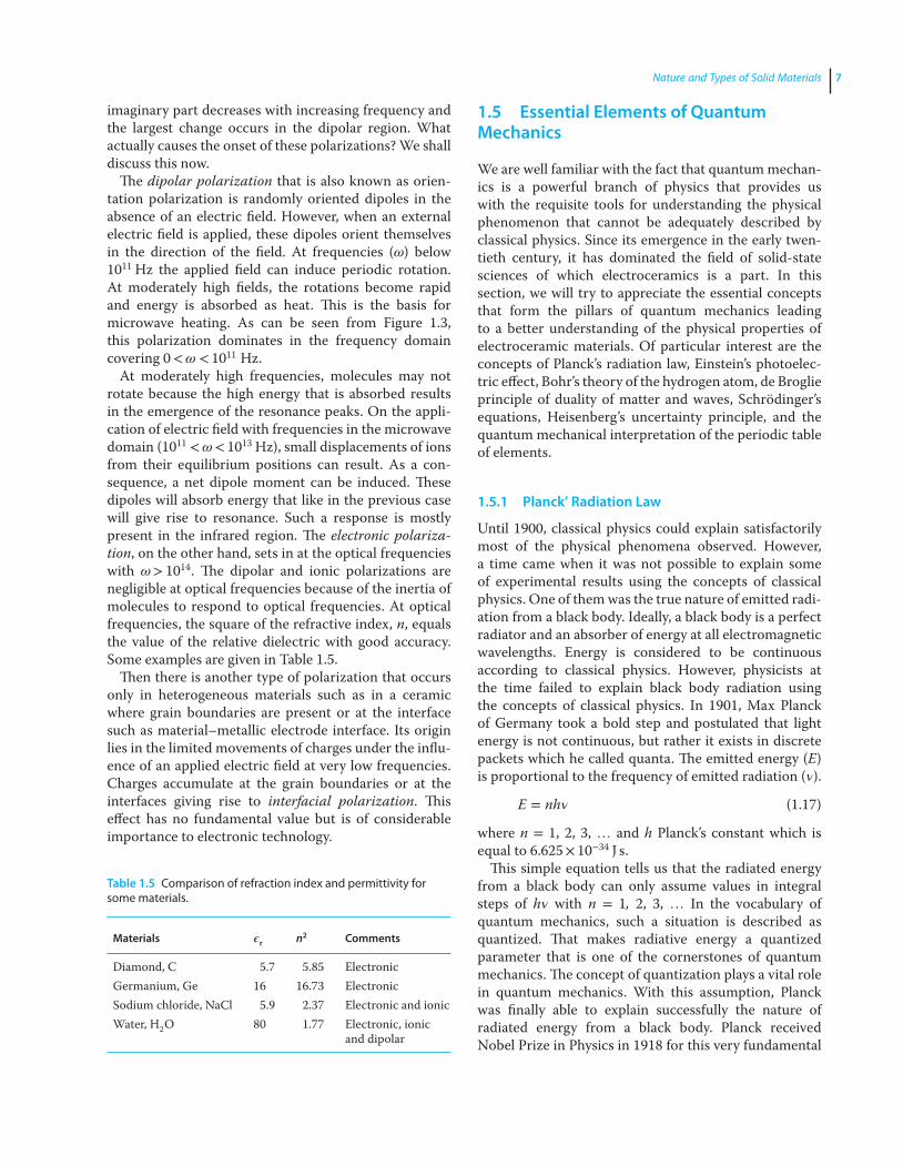
calculated the radii of the orbits and their respectiveangular momenta for different spectral series, and thesecalculations were found to be in agreement with exper-imentally determined values. In Figure 1.7, the Bohr’smodel of hydrogen atom is shown. Here p+ and e−represent the positively charged protons and negativelycharged electrons, respectively. It also shows the energyemitted by the electron when transiting between theorbits n = 1, 2, 3.
Since the orbits are quantized, its energies must alsobe quantized, which would lead to the onset of discretespectra. In the emission and absorption processes, pho-tons are involved whose energy is quantized. Therefore,the change in energy during the transition from one orbitto another must satisfy the following condition.
ΔE = h𝜈 = Ef − Ei (1.25)
where Ei and Ef refer to the energies of the initial and finalorbits involved in the transition.
We know that the hydrogen atom is the simplestelement of the periodic table having the atomic num-ber, Z= 1. Bohr’s elaborate calculation resulted in the
Nature and Types of Solid Materials 11
n=2
+
n= 3
n= 1
hν
hν
e–
e–e–
Figure 1.7 Bohr’s model of hydrogen atom.
ground-state energy, E0 (when n = 1) for the hydrogenatom to be
E0 = 1h2
(mee4
8𝜖20
)= 13.6 eV (1.26)
Similarly, the energy of the nth orbit is given byEq. (1.27).
En = −(13.6
n2
)eV (1.27)
Substituting these values in Eq. (1.27) we arrive atEq. (1.28).
h𝜈 = 13.6
(1n2
i− 1
n2f
)(1.28)
Since c = 𝜈𝜆 where c is the velocity of light and 𝜆 itswavelength, we can rewrite Eq. (1.28) as Eq. (1.29).
1𝜆= 13.6
ch
(1n2
i− 1
n2f
)≈ R
(1n2
i− 1
n2f
)(1.29)
By substituting the values of the universal constants cand h in ( 13.6
ch) one gets 1.097× 10⁷ m−1, which is the value
of the Rydberg constant used in spectroscopy.In summary, we can conclude that the Bohr’s theory
satisfactorily explains the experimental results of theatomic spectra of the hydrogen atom and thereby couldsolve the longstanding problem of classical physics.Therefore, his assumptions were intuitively correct thatthe orbits are quantized and that the Rydberg constant isnot an arbitrary number to fit an experiment but ratherit is the combination of fundamental constants like thecharge of the electron, its mass, Planck’s constant andthe permittivity of vacuum.
It should also be recognized that in spite of the successof Bohr’s theory in explaining the spectrum of the hydro-gen atom and giving us the concept of the quantization ofangular momentum it has some fundamental flaws. Forexample, it is in violation of the Heisenberg UncertaintyPrinciple, and it cannot explain the Zeeman Effect whenthe spectral lines split up in several components in thepresence of a magnetic field.
1.5.4 Matter–Wave Duality: de Broglie Hypothesis
Planck gave the concept of energy being quantized,Einstein gave the concept of photons that can behave likea particle yet has no mass, and Bohr advanced quantummechanics that was in its infancy by proposing theangular momentum to be quantized. All these ground-breaking concepts point to the particle-like behaviorof light that was well established to be wave-like byelectromagnetic theory. This leads us to the questionof how can a particle (such as an electron) also acquirewave-like characteristics?
The answer was provided by Louis de Broglie of Francein 1923 in his famous hypothesis of matter–wave duality.This led to the development of the famous Schrödinger’sequation that firmly anchored quantum mechanics asthe new physics. de Broglie based his hypothesis ontwo well-established results. He considered Einstein’smatter–energy equation and Planck’s theory of lightquanta.
Einstein’s matter–energy equation states that
E = mec2 (1.30)
And Planck’s law of radiation says that
E = h𝜈 (1.31)
de Broglie argued that since particles and waves havethe same traits, the two energies must be equal. Combin-ing these two equations Eq. (1.32) results.
mec2 = h𝜈 (1.32)
Considering that the real particles, such as an electron,cannot acquire the velocity equal to the velocity of light,we need to modify the above equation slightly to use itfor real particles. Let us assume that we are dealing withelectrons with the mass, me and velocity, ve. Furthermore,we can substitute for the frequency
(ve
𝜆e
), where 𝜆e is the
wavelength associated with an electron. These manipula-tions result in Eq. (1.33).
𝜆e =h
meve= h
2π
(2πpe
)= 2𝜋ℏ
pe(1.33)
where pe is the momentum of the electron. We can alsowrite Eq. (1.33) as Eq. (1.34) which is the standard form
12 Fundamentals of Electroceramics
of de Broglie’s relationship.
pe =h𝜆e
= ℏke (1.34)
where ke is the wave number which by definition is(
2π𝜆e
).
This simple equation derived from another twovery simple equations may look humble, but it hasfar-reaching consequences in solid-state physics andelectronics. de Broglie was awarded the Nobel Prize inPhysics in 1929 for this contribution. Its experimentalproof was given by Clinton Davisson and Lester Germer,both American Physicists, in 1925 confirming the wavenature of electron. For this contribution, they too sharedthe Nobel Prize in Physics in 1937.
1.5.5 Schrödinger’s Wave Equation
What Newton’s laws of motion and his concept ofconservation of energy are to classical physics so isthe Schrödinger’s equation to quantum mechanics.He is one of the giants of physics of the twentiethcentury and belongs to the class of Sir Isaac Newton.The matter–wave duality hypothesis of de Broglieis the nucleating factor for Schrödinger’s equation.Schrödinger argued that since particles can have a wave-length associated with them, they must be representedby a wave equation.
Schrödinger’s equation predicts the future behavior ofelectrons in a dynamic frame work. It is the probabilityof finding an electron in events to come. A partial dif-ferential equation describes how the quantum state of aquantum system changes with time. This is the corner-stone of quantum mechanics that opened up multipleavenues to evolve and advance. It was formulated in 1926by Erwin Schrödinger, a brilliant theoretical physicistof Austria. It earned him, of course, the Nobel Prize inphysics in 1933. It should be remembered that thereis no formal derivation of Schrödinger’s equation. It isintuitive and Schrödinger simply wrote it. It was imme-diately accepted by other geniuses of his time and hasnever been challenged. One of the greatest theoreticalphysicists of our time, Richard Feynman, is quoted tohave said, “Where did we get that from? It is not possibleto derive it from anything you know. It came out of themind of Schrödinger?”
Let us now write the one-dimensional form ofSchrödinger’s equation.
d2𝜓
dx2 +2me
ℏ2 (E − V )𝜓 = 0 (1.35)
Here𝜓 is the wave function, E the total energy, and V thepotential energy. The kinetic energy of the electron thenis equal to (E −V ).
In its three-dimensional form, Eq. (1.35) becomesEq. (1.36) on substituting the first term on the left sidewith the Laplacian operator ∇2 =
(𝛿2
𝛿x2 +𝛿2
𝛿y2 +𝛿2
𝛿z2
).
∇2𝜓 +2me
ℏ2 (E − V )𝜓 = 0 (1.36)
The question now arises about the exact nature of theSchrödinger’s wave function, 𝜓 . What is it, and how is itsignificant in a real physical system? The answer is pro-vided by Max Born (Nobel Prize in Physics in 1954) ofGermany in 1926. He postulated that the quantity |𝜓|2
must represent the probability of finding an electron ina unit volume at the time at which the wave function,𝜓 , is being considered. Alternatively, |𝜓|2 predicts thepresence of an electron in a space, dv. That amounts tonormalizing the wave function as in Eq. (1.37).
∫+∞
−∞|𝜓|2dv = 1 (1.37)
Equation (1.37) sets the boundary conditions that thesolutions for wave function, 𝜓 , must obey. The otherboundary conditions imposed on the wave functions are(i) they must be continuous and (ii) mathematically wellbehaved. This amounts to telling us that 𝜓(x) must be acontinuously varying function of x and its first derivativewith respect to x, d𝜓/dx, must also be a continuousfunction of x.
Another form of the Schrödinger’s equation can berepresented using the Hamiltonian operator that is thesum of the kinetic and potential energy in quantummechanics. The operator is named after Sir WilliamHamilton, a reputed physicist of Ireland who lived inthe nineteenth century. He is best known for the devel-opment of Hamiltonian mechanics that is essentiallythe reformulation of Newton’s mechanics. If T is thekinetic energy and V the potential energy, then thecorresponding Hamiltonian takes the form of Eq. (1.38).
H = T + V (1.38)
Here the potential energy operation V is equivalent to thespace and time variants of the potential energy, V . Themomentum, p, in operator form is written as:
p = −iℏ∇ (1.39)
Similarly, the kinetic energy operator form is as inEq. (1.40).
T =p2
2me= − ℏ2
2me∇2 (1.40)
Substituting these two equations in Eq. (1.38), we getthe Hamiltonian operator, H , as in Eq. (1.41).
H = − ℏ2
2me∇2 + V (r, t) (1.41)
Nature and Types of Solid Materials 13
We can now rewrite the time-independent Schrödinger’sequation in terms of the Hamiltonian H , as
H𝜓i = Ei𝜓i (1.42)
Here 𝜓 i is called the eigenfunctions and Ei the eigenval-ues of energy.
The Hamiltonian operator also lead us to thetime-dependent Schrödinger’s equation which is givenby Eq. (1.43).
H𝜓 = iℏ(𝛿𝜓
𝛿t
)(1.43)
The probability of finding an electron in the volumeelement (dx dy dz) at a time t is then given by|𝜓(x, y, z, t)|2dx dy dz
Exercise 1.2Express the time-independent Schrödinger’s equation interms of the momentum.
SolutionWe have the standard form of the time-independentSchrödinger’s equation containing the energy term inEq. (1.36).
(E −V ) is the kinetic energy T of the electron; then itfollows from Eq. (1.36) hat
∇2𝜓 = −[ℏ2
2meT]𝜓 (a)
Equation (b) gives us the kinetic energy in term of themomentum, pe of the electron.
T = k.e. = 12
mev2 = 12
(m2ev2
me
)=
p2e
2me(b)
Substituting this in Eq. (a) and after a little rearrange-ment, we get Eqs. (c) and (d).
∇2𝜓 = − ℏ2
2me
(p2
2me
)𝜓 = −
[(ℏ
2me
)2
p2e
]𝜓 (c)
∇2𝜓 = −(ℏpe
2me
)2
𝜓 (d)
Equation (d) is the momentum form of Eq. (1.36).
1.5.6 Heisneberg’s Uncertainty Principle
We learned in the previous section that the Schrödinger’sequation is statistical in nature and can predict the proba-bility of an event happening but cannot predict accuratelyeither the position of an electron or its velocity. Similarly,it is not possible to predict either the momentum in aparticular space in which the electron finds itself nor theenergy it might acquire in a particular instant of time.The reason being that the uncertainty principle forbids
the measurements of two complimentary parametersconcurrently with arbitrary accuracy. The theory wasdeveloped by Werner Heisenberg (Nobel Prize in Physicsin 1932) of Germany in 1927.
The essence of this theory is that the product of twocomplimentary variables cannot be less than a constantvalue. For example, if position x and momentum p areconsidered, then the uncertainty in position Δx andmomentum Δp is given by the following inequality.
Δx × Δp ≥ ℏ ≈ 10−34 J s (1.44)
Similarly, the uncertainty in energy E and time t can beexpressed as follows:
ΔE × Δt ≥ ℏ ≈ 10−34 J s (1.45)
One can draw the conclusion that if one tries tomeasure one physical parameter with arbitrarily highprecision, the uncertainty in measuring the other con-jugate parameter becomes larger. The more the particlebecomes smaller such as atomic and subatomic particles,the accuracy in determining their two complimentaryvariables cannot exceed the limits of ≈10−34 set by theuncertainty principle. One should remember that itis not a reflection on the inaccuracy of measurementinstruments or the methods used for experimentation. Itis simply inherent in the quantum mechanical interpre-tation of nature. As the particles approach macroscopicscales, the uncertainty decreases drastically. To illustratethis point, let us consider a mass m, which is 103 timesgreater than the mass of an electron. If the velocity ofthe particle is v, its momentum p = mv and Δp = mΔv.Substituting this in Eq. (1.44) for ΔP, we get Eq. (1.45).
Δx × Δv ≥ ℏ
103me≈ 10−4 J s kg−1 (1.46)
The uncertainty has decreased by 1000-fold for amacroscopic system whose characteristics can be deter-mined individually with greater accuracy. Nevertheless,it is to be learned from Eq. (1.46) that both the velocityof a particle and its position cannot be measured witharbitrary accuracy at the same instant.
1.6 Quantum Numbers
The wave function,𝜓 , describes the probability of findingan electron at certain energy levels within an atom. Sinceit is associated with an electron in an atom it is alsocalled the atomic orbital. It defines a region in space inwhich the probability of finding an electron is high. Toevery such electron, there are four quantum numbersassociated with it which are its defining characteristics.We have already discussed two of them; the principalquantum number, n, and the orbital quantum number, l.
14 Fundamentals of Electroceramics
The other two are magnetic quantum number, ml, andthe spin quantum number, s. We now describe all four insome detail.
I. Principal quantum number, n: Allowed values areonly integers ranging from 1 to ∞. It determinesthe total energy of the electron; and the number oforbitals (=n2) having different energy levels.
II. Orbital quantum number, l: Allowed values are from0 to (n− 1).The second quantum number is the orbital quantumnumber and is directly associated with the principalquantum number, n. It is also referred to as angularmomentum quantum number and azimuthal quan-tum number. We already discussed previously that italso is allowed to have only integral values. It dividesthe shells into smaller group of subshells identifiedby letters such as s, p, d, f, g, etc. The origin of such anomenclature lies in optical spectroscopy where theemission or absorption processes were identified ass (sharp), p (principal), d (diffused), f (fundamental),g (ground), etc. After the discovery of quantummechanics, it was realized that these spectral seriescorrespond to specific values of the orbital quantumnumbers as shown in Table 1.7.The term “subshells” are preferred by chemists,whereas physicists prefer the term “orbitals.” Theother designation assigned to the subshells ororbitals with certain values of l are called the Bohrdesignation of atomic subshells with the letter of K,L, M, N, etc. This designation is followed by expertsof X-ray diffraction. The total number of orbitals(or subshells) is given by 2n2. That is, there are twoorbitals for n = 1; 8 for n = 2, 18 for n = 3, 32 forn = 4, and so forth. Table 1.7 lists them all.If n = 1, then l = 0, the orbital is called 1s; if n = 2 andl = 0, the orbital is called 2s; and if n = 3 and l = 0,the orbital is 3s. Other identifiers follow the samelogic. So far as the orbital energy (E) is concerned, itincreases with increasing orbital quantum number,l. It follows the sequence: Es <Ep <Ed <Ef <Eg.Their relative energy levels follow the sequence of1s< 2s< 2p< 3s< 3p< 3d< 4s< 4p< 4d< 4f< 5s –and so forth.
III. Magnetic quantum number, ml: Its allowed values areml = 0 to ±l with total number of ml being (2l + 1).
Table 1.7 Correspondence of spectral series with orbital quantumnumber, l from 0 to 4.
Orbital quantum number, l 0 1 2 3 4
Spectral series s p d f g
From Amperé’s law, we know that a moving chargegenerates an electric current which in turn caninduce a magnetic field when enclosed in a loop(such as an orbit). That is the reason that thisquantum number is called the magnetic quantumnumber and as such it is supposed to be direc-tional. It can assume any of the (2l + 1) differentdirections. This was indeed shown to be the caseexperimentally by Otto Stern and Walther Gerlach,both German physicists, in 1922. They confirmedthat the magnetic moments are quantized and canorient only in certain directions. For this groundbreaking work Stern was recognized with the NobelPrize in Physics in 1943, but Gerlach was excludedapparently because of his association with the NaziRegime.
IV. Spin quantum number, s: Allowed values + 12
or − 12.
In an atomic system, electrons can reside in differ-ent orbits. They are allowed to move around the orbitwhile at the same time spinning around its own axis.A spinning electron generates a magnetic field withtwo well defined orientations. These orientations aredesignated as either “up (↑)” or “down (↓).” Alterna-tively, it can only have the values of =± 1
2.
In Table 1.8, we present a list of values for orbital andmagnetic quantum numbers with respect to the values ofthe principal quantum number. Their resulting spectro-graphic and Bohr designations are also given there.
1.7 Pauli Exclusion Principle
The four quantum numbers define a wave function of anelectron fully and completely. They define its quantumstate, its energy, and almost any other characteristicsassociated with it. The orbital quantum number, l, andmagnetic quantum number, ml, can each have multiplevalues for any fixed value of the principal quantumnumbering as outlined in Table 1.8. What happens whenthere are a large number of electrons present in a system?This can cause an enormous challenge to sort out theirquantum states leading to utter confusion.
This is where the selection rule conceived by WolfgangPauli of Austria in 1925 comes to our rescue. This rule isuniversally known as the Pauli’s Exclusion Principle forwhich he received the Nobel Prize in Physics in 1945. Itstates that: No two electrons in an atom can have exactlythe same set of four quantum number; the spins mustbe antiparallel. This simply means that there can betwo electrons for each combination of n, l, and ml, buttheir spin orientations must be antiparallel. Followingthis rule, we can assign 2 electrons to each s-state, 6 toeach p-state, 10 to each d-state, 14 to each f-state, and
Nature and Types of Solid Materials 15
Table 1.8 Relationship between n, l, and ml , and their spectrographic and Bohr designations.
Source: From Leonid 1963 [1]. Azaroff and Brophy (1963).
so forth. They vary in arithmetic progression with fourbeing the common difference. It is important to note thatthis selection rule is not arbitrary, rather it is based onsound mathematical principles of quantum relativisticphysics. A full mathematical treatment of Pauli exclusionprinciple is beyond the scope of this book.
1.8 Periodic Table of Elements
The periodic table of elements was originally devel-oped by the Russian chemist with the name of DmitriMendeleev in 1869. He arranged all the elements knownuntil that time (about 60) in rows and columns accordingto their atomic weight and chemical properties. Manymore elements have since been discovered since, andthey all can be arranged in the periodic table on thebasis of their atomic numbers, chemical properties,and electronic configurations. The periodic table is anindispensable tool available to scientists and engineersengaged in the study of chemical systems and materials.The modern periodic table consists of eight columns andseven rows.
To take the full benefit of the subject matter coveredin this section, it is advisable that readers should have amodern copy of the periodic table readily available. Thereare many sources from which one can get a good copy ofthe Periodic Table. The NIST (National Institute of Stan-dards and Technology) in the United States may be a reli-able source.
The discovery of quantum numbers greatly shapedthe periodic table resulting in advancement to the fieldsof chemistry, physics, and materials science. Elementsfound in the same column are referred to as belonging tothe same group such as Groups I, II, III, IV, V, etc., as they
are similar in their chemical properties. There are a totalof eight groups, many of which are subdivided in A andB subgroups in many of today’s periodic tables. The rowsin the periodic table are called periods. There are sevenperiods in which elements are arranged with increasingvalues of atomic numbers. For example, hydrogen withits atomic number (Z) of 1 is the first element of theperiodic table, then comes He with Z = 2 followed bylithium with Z = 3, and so on. Currently, the highestatomic number of Z = 118 belonging to the artificiallysynthesized ununoctium (also known as eka-radon) withthe chemical symbol of Uuo. It is radioactive and veryunstable. With its discovery in 2002, the seventh periodof the periodic table is complete and a new period begins.The heaviest naturally found element is uranium-238(U-238) with Z = 92. It is a well-established radioactivematerial with the half-life time of ≈4.5 billion years. Theheaviest stable element is bismuth (Bi) with Z = 83 anddensity = 11.34 g cm−3.
Each element has its unique atomic electronic config-uration based on the number of the principal quantumnumber, n, its atomic number, and the number of elec-trons in each orbit as dictated by the Pauli exclusion prin-ciple. For example, our lightest element is hydrogen withZ = 1 only and its electronic configuration is written as1s1. The rule for writing the electronic configuration ofan element can be described as follows: “The integer onthe left refers to the value on the principal quantum num-ber, n; followed by the orbital (s, p, d, f, etc.) and then asuperscript giving the number of electrons found in eachorbital.” The filling sequence follows in the order of s, p,d, f, etc.
The electrons in the outermost orbital are technicallycalled the valence electrons. The valence electrons playa decisive role in initiating a chemical reaction and in
16 Fundamentals of Electroceramics
forming chemical bonds between atoms which makes astructure stable. They can be shared with other atoms giv-ing rise to chemical bonds known as ionic, metallic, andcovalent. The concept of valence electrons is also veryimportant to solid-state sciences, materials science, andelectroceramics because they help us in developing mod-els and theories for understanding electronic propertiesand physical phenomena displayed by materials.
Following the rule stated above, electrons in an atomcan be divided between different orbitals. Let us nowwrite electronic configurations for the second and thirdelements of the periodic table. The second element is He(Z = 2), and its electronic configuration is 1s2, and thethird element Li (Z = 3) has the configuration of 1s22s1
which is equivalent to [He]2s1. This short cut simplytells us that the first two s-electrons of Li have the sameconfiguration as He and the third electron moves to thehigher orbital. This makes it easier to assign electronicconfigurations of elements with higher values of atomicnumbers.
Let us now consider the elements of the Group VIII thatis the home of the seven noble gases. Each of them rep-resents the completion of the period in which they resideand the beginning of the next period. We present theirelectronic configuration in Table 1.9.
These elements are called the noble gases because theyare to a great extent chemically inert. They represent
Table 1.9 Elements of Group VIII.
Elements Helium, He Neon, Ne Argon, Ar Krypton, Kr Xenon, Xe Radon, Rn
the configurations with maximum allowable electrons ineach subshell leaving no vacancy at all.
We stated already that many of the physical proper-ties and phenomena exhibited by materials can be bestexplained based on the value of the valence electronspresent. The tables that follow include some elementsare of great interest (Table 1.10).
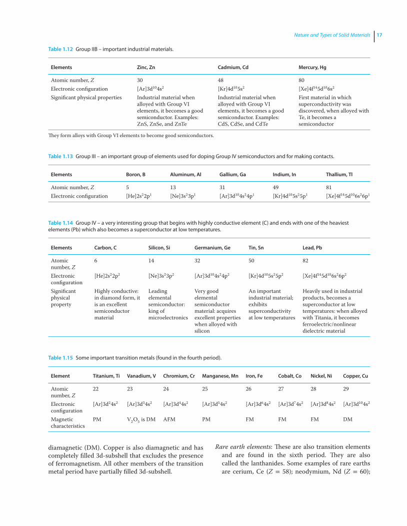
Notice that each of these elements have just ones-valence electrons and represents the beginning ofa new group. Chemically, the alkali metals are highlyreactive (Tables 1.11–1.13).
Ga and In also form very important semiconduc-tor materials when alloyed with certain members ofGroup V. Al, of course, is a heavily used metal for trans-mission of electrical power and makes good contactswith semiconductors and dielectrics (Table 1.14).
There is large number of elements classified as tran-sition metals, and they are found in Groups III throughVIII. We include here in our table only those found in thefourth period with Z = 22–29. They are characterized bythe occupancy of their 3-d subshell. They exhibit interest-ing magnetic properties. Chemically, they have multipleoxidation states (Table 1.15).
Fe, Co, and Ni are the only 3-d elements that are alsostrongly ferromagnetic (FM). Ti and Mn are param-agnetic (PM), Cr is antiferromagnetic (AFM), whereasthe magnetic nature of V is unknown but as V2O5 it is
Nature and Types of Solid Materials 17
Table 1.12 Group IIB – important industrial materials.
Elements Zinc, Zn Cadmium, Cd Mercury, Hg
Atomic number, Z 30 48 80Electronic configuration [Ar]3d104s2 [Kr]4d105s2 [Xe]4f145d106s2
Significant physical properties Industrial material whenalloyed with Group VIelements, it becomes a goodsemiconductor. Examples:ZnS, ZnSe, and ZnTe
Industrial material whenalloyed with Group VIelements, it becomes a goodsemiconductor. Examples:CdS, CdSe, and CdTe
First material in whichsuperconductivity wasdiscovered, when alloyed withTe, it becomes asemiconductor
They form alloys with Group VI elements to become good semiconductors.
Table 1.13 Group III – an important group of elements used for doping Group IV semiconductors and for making contacts.
Elements Boron, B Aluminum, Al Gallium, Ga Indium, In Thallium, Tl
Table 1.14 Group IV – a very interesting group that begins with highly conductive element (C) and ends with one of the heaviestelements (Pb) which also becomes a superconductor at low temperatures.
Elements Carbon, C Silicon, Si Germanium, Ge Tin, Sn Lead, Pb
Very goodelementalsemiconductormaterial: acquiresexcellent propertieswhen alloyed withsilicon
An importantindustrial material;exhibitssuperconductivityat low temperatures
Heavily used in industrialproducts, becomes asuperconductor at lowtemperatures: when alloyedwith Titania, it becomesferroelectric/nonlineardielectric material
Table 1.15 Some important transition metals (found in the fourth period).
Element Titanium, Ti Vanadium, V Chromium, Cr Manganese, Mn Iron, Fe Cobalt, Co Nickel, Ni Copper, Cu
diamagnetic (DM). Copper is also diamagnetic and hascompletely filled 3d-subshell that excludes the presenceof ferromagnetism. All other members of the transitionmetal period have partially filled 3d-subshell.
Rare earth elements: These are also transition elementsand are found in the sixth period. They are alsocalled the lanthanides. Some examples of rare earthsare cerium, Ce (Z = 58); neodymium, Nd (Z = 60);
18 Fundamentals of Electroceramics
samarium, Sm (Z = 62); europium, Eu (Z = 63); andgadolinium, Gd (Z = 64).
Radioactive elements: Elements of the seventh period arecalled the actinides or radioactive elements. They arealso classified as transition elements. Some of theseinclude the following thorium, Th (Z = 90); uranium,U (Z = 92); plutonium, Pu (Z = 94), and americium,Am (Z = 95).
1.9 Some Important Concepts ofSolid-State Physics
1.9.1 Ceramic Superconductivity
The superconductivity was discovered in 1911 at theUniversity of Leiden in the Netherlands by Heike Kamer-lingh Onnes. He was awarded the Nobel Prize in Physicsin 1913 for the production of very low temperatures.It was in mercury that he found the resistance becamenonexistent when cooled to 4.2 K. He also discoveredsuperconductivity properties in lead and tin. The tablethat follows lists the ground-breaking advancement inthe field of superconductivity since its discovery. Since1911 until 1987 superconductivity was found mostly inmetallic systems at very low temperatures. It was in 1987that superconductivity was observed for the first time inceramic compounds at relatively high temperatures. Thislandmark discovery dramatically changed the field ofsuperconductivity from being a curiosity of fundamental
science to be of great importance to technology. Someof these issues we discuss in this section. The natureof this book does not allow us to discuss this topic indetail. However, interested readers may wish to consulta good book on superconductivity for advanced studies;we recommend the book by Orlando and Delin [2]. Thisfield has produced a number of Nobel laureates. We listthem in Table 1.16.
As already stated until 1985, superconductivity wasobserved only in metals and their alloys with the upper-most critical temperature of 20 K. Then it increased to35 K with the discovery of superconductivity in a ceramicsample of Ba–La–Cu-oxide. The discovery was made inJanuary of 1986 at IBM Zurich Laboratories by GeorgBednorz and K. Alex Müller who were awarded NobelPrize in Physics in 1987. This landmark discovery wasa paradigm shift in solid-state physics for two reasons:first, the critical point for superconductivity crossedthe boiling point of Ne (27 K≈−246 ∘C) and second,the superconductivity was found in a ceramic systemagainst all prevailing concepts of physics at the time.By now many more oxide superconductors have beendiscovered, and we list some of them in Table 1.17.
It is interesting that the crystal structure of theseoxides happen to be perovskite (ABO3), which is theleading group in which prominent nonlinear dielectricssuch as ferroelectrics are found.
So far as an explanation of this interesting physical phe-nomenon is concerned, there is only one unified theorythat can explain superconductivity and even that is not
Table 1.16 List of Nobel Prize in Physics awarded for superconductivity.
Name Year Contribution
Heike Kamerlingh Onnes 1913 Discovery of superconductivityJohn Bardeen, Leon N. Cooper, and J. Robert Schrieffer 1972 BCS theory of superconductivityLeo Esaki, Ivar Giaever, and Brian D. Josephson 1973 Josephson tunneling effectGeorg Bednorz and K. Alex Müller 1987 High temperature superconductivity (ceramic
superconductivity)Alexi A. Abrikosov, Vitaly L. Ginzburg, and Anthony J. Leggett 2003 Theory of superconductivity and superfluids
Table 1.17 List of some ceramic superconductor materials.
Ceramic superconductors Critical point, TC (K) Number of Cu–O planes/unit cell Crystal structure Crystal unit cell
Note all critical points are above the liquid nitrogen temperature of 77 K (−196 ∘C).Source: https://en.m.wikipedia.org/wiki/Hightemperature_Superconductivity. Licensed under CC BY 3.0.
Nature and Types of Solid Materials 19
adequate to handle the superconductivity found in oxidesystems. In 1972, almost 60 years after the discovery ofsuperconductivity, a macroscopic theory was developedby three American Physicists named John Bardeen, LeonCopper, and J. Robert Schrieffer that has been success-ful in explaining the superconductivity found in metallicsystems at low temperatures. The theory is also known asBCS theory, and the three physicists were awarded NobelPrize in Physics in 1972 for developing this elegant the-ory. This was the second Nobel Prize for John Bardeen,the first one was for the discovery of transistors in 1956.
The BCS theory requires a sound knowledge ofadvanced physics and therefore is beyond the scope ofthis textbook. The central point of this theory is the con-cept of so-called Copper pairs. In the superconductingphase Cooper pairs can form when two electrons couplewith antiparallel spins. Cooper pairs can behave verydifferently than single electrons that must obey the PauliExclusion Principle, whereas the Cooper pairs behavemore like bosons that can condense in the same energylevels. The Copper pairs are also called superconduct-ing electrons. Though the BCS theory has been verysuccessful in explaining conventional superconductivitysatisfactorily, it appears not to be applicable to ceramicsuperconductivity. Various groups of theoreticians arecurrently working on this problem, and we hope one daysoon we might have a good theory of superconductivityfound in electroceramics.
1.9.2 Superconductivity and Technology
Superconductivity is a unique physical phenomenonpoised to play a vital role in the evolution of newtechnology. A large number of devices and applica-tions have been proposed based on magnetic andelectronic properties of superconductivity that we willdiscuss subsequently in this chapter. Production ofvery high magnetic fields, Josephson junctions, andsuperconducting quantum interference device (SQUID)magnetometers are so far the most established tech-nologies based on low temperature superconductingmaterials. They operate only at cryogenic temperatures.However, a large number of applications, from highlysophisticated to straightforward and simple, have beenproposed based on ceramic superconductors with criti-cal temperatures far above cryogenic temperatures. Forthese proposals to be more useful, and commerciallyviable, room-temperature superconducting materialshave to be discovered. The hope is pinned on newceramic materials because it will be possible to producethem in high volumes and in high quality at reasonablecosts.
Superconducting magnets can produce fields fargreater than those generated by the most powerful
electromagnets. Currently, the highest sustained mag-netic fields achieved are about 8.3 T (=8.3× 10⁵ G) byniobium–titanium (Nb–Ti) superconducting magnetsthat operate at the extremely low temperature of 1.9 K.The magnetic fields are measured in the units of Teslaand Gauss, and they are abbreviated as T and G, respec-tively. Superconducting magnets are universally usedin magnetic resonance imaging (MRI) machines thatis a powerful diagnostic tool indispensable to healthprofessionals as well as of great significance to scientistsfor new discoveries. One of the most intriguing aspectsof these magnets is the onset of persistent currents.Once the magnet is energized the windings of Nb–Tibecome superconducting closed loops at about 1.9 Kgiving rise to a persistent current following the Faraday’slaw of induction. This law states that a magnetic fieldcan induce a current in a conducting loop accordingto L
(dIdt
)= −a
(dBdt
)where L is the inductance, I the
current, and B the magnetic flux. The current generatedin a superconducting loop can flow for months even inthe absence of an external magnetic field. At this point,the external power supply can be turned off, and themagnetic field is sustained by the persistent current. Wewill learn more about it later while studying the magneticproperties of superconducting materials.
Another very powerful superconducting device is theSQUID magnetometer based on the Josephson junctioneffect that establishes the tunneling of the Copper pairs.There are many other unique applications based on thiseffect, and we will discuss some of them when we studythe Josephson effect.
1.10 Signature Properties ofSuperconductors
Temperature, magnetic field, and pressure are threeexternal agents that can greatly alter the fundamentalnature of a superconducting material by switching themfrom normal phase to superconducting phase, and viceversa. Infinite electrical conductivity and the onset ofdiamagnetism below a critical temperature are the twomost important properties of a superconductor material.We discuss both these properties in the next sectionshere. It is known that a large number of elements ofthe periodic table become superconducting at a criticaltemperature and a critical pressure. Recently, it has beenreported that H3S becomes superconducting with a crit-ical temperature (TC) of 203 K at 150 GPa of pressure.2This is the highest transition point reported so far for
2 Reported in Physics Today of July 2016 about this discovery made byMikhail Eremetes and his team at the Max Planck Institute ofChemistry in Germany.
20 Fundamentals of Electroceramics
any superconducting material. H3S belongs to the samefamily of chemicals as hydrogen sulfide (H2S) which ispresent in almost any chemistry laboratory and has anoxious smell.
1.10.1 Thermal Behavior of Resistivity of aSuperconductor
Superconductivity can be defined most simply by statingthat below a critical temperature a superconductor com-pletely loses its resistivity resulting in the conductivity tobe infinite. The critical temperature is also known as crit-ical point or superconducting transition temperature oreven superconducting transition point. Its universal sym-bol is TC. The temperature dependence of resistance of asuperconductor material is presented in Figure 1.8.
Here we find two distinct phases to exist: one above thecritical point, TC, and the other below this point. As wecan see from the figure, a superconducting material goesfrom its normal state at T >TC to its superconductingstate at T <TC undergoing a phase change at T = TC.The transition from the normal state to the supercon-ducting state is governed by the relationship describedby Eq. (1.47).
𝜎 ≈ CT − TC
(1.47)
When T = TC the conductivity, 𝜎, is infinite. Thermo-dynamically, it is a phase change of the second order.Equation (1.47) is the standard form of the Curie–Weisslaw that is obeyed by ferromagnetic and ferroelec-tric materials where we also encounter similar phasetransitions at their respective critical temperaturescalled the Curie temperatures, TC. We will learn about
0
Normal state
T>Tc
Superconducting
state
T<Tc
0
Resistance,
R (Ω)
Critical point, Tc Temperature (K)
Figure 1.8 Resistivity as a function of temperature for asuperconducting material.
ferroelectricity and ferromagnetism in the other chaptersin this book.
The state of infinite conductivity persists so long asthe temperature is below the critical point of TC. It isa significant result and obviously of great importanceto power transmission technology. All metals lose partof the original electric power by Joule heating (≈I2R)due to a nonzero resistance. Over the course of time,this loss can be significant. The hope is that one daywe will be able to use superconducting wires instead ofmetallic wires to transmit electric power from one pointto another and thereby completely eliminate the loss ofpower.
We can easily imagine the benefit of such a system toconsumers and industry. This dream can only be fulfilledif a room temperature superconducting material is dis-covered. Today, we are not there, but science is work-ing diligently to reach that goal post. The discovery ofceramic superconductor has given us a roadmap to reachthis destination and the race is intense.
1.10.2 Magnetic Nature of Superconductivity:Meissner–Ochsenfeld Effect
We concluded in the previous section that all supercon-ductors become ideal conductors (𝜎→∞) below theircritical temperatures. They also become ideal diamag-netic materials (magnetic susceptibility,𝜒 = − 1) in thesuperconducting phase. This remarkable property wasconfirmed by the Meissner–Ochsenfeld effect, which isreferred erroneously in many circles only as the Meissnereffect. The Meissner–Ochsenfeld effect was discoveredin Germany in 1933 by Walther Meissner and RobertOchsenfeld. It states that in the superconducting phase,the magnetic flux lines are expelled after it reachesa certain depth below the surface. This is called theLondon penetration depth and is associated with thesuperconducting electron density. It decays exponen-tially within the interior of the superconducting phase.Once the London penetration depth is reached, themagnetic field stops penetrating the sample, which thenbecomes an ideal diamagnetic material. Diamagnetismis characterized by the capacity of a material to opposethe penetration of magnetic flux lines below its surface.This is in contrast to the nature of a ferromagnetic or aparamagnetic material in which magnetic flux lines canpenetrate unopposed. The Meissner–Ochsenfeld effectcannot be explained by classical physics, and the explana-tion is provided by quantum mechanics establishing thefact that the superconductivity is a quantum mechanicalphenomenon. Mathematically, the London-penetratingdepth is given by
𝜆L =(𝜖0mec2
ne2
) 12
(1.48)
Nature and Types of Solid Materials 21
YBCO sample
Centralmagnets
Top magnet
Figure 1.9 Magnetic double levitation by 123 YBCO insuperconducting state.
where n is the superconducting electron density. Theparameters 𝜖0, c, me, and e are physical constants asdefined already above.
Another critical property associated with supercon-ductivity is called the coherence length. It is related tothe energy gap and the Fermi velocity of the supercon-ducting phase. It bears no relationship with the Londonpenetration depth. Both the coherence length and theLondon penetration depth have been experimentallydetermined for a number of superconducting materials.Its magnitude usually is in the nanometers range.
The Meissner–Ochsenfeld effect can be demonstratedeasily by cooling a 123 YBCO ceramic sample below itscritical point using liquid nitrogen (≈77 K).
Once superconductivity sets in, the sample becomesdiamagnetic facilitating the levitation of a magnet in airabove the sample surface, which can be seen in Figure 1.9.As expected, the magnetic flux lines are expelled result-ing in the magnetic levitation. In Figure 1.9, the doublelevitation was achieved by floating a ceramic magnet ontop of another magnet.3
It is not only the temperature that defines the super-conducting phase. Also under the influence of anexternal magnetic field, H , the superconducting phasecan switch to the normal phase. The magnitude of thefield that can induce this phase change in called thecritical magnetic field (HC), and it is found to be stronglytemperature-dependent as we can see from Figure 1.10.Here, each combination of HC1-T1 and HC2-T2 is capableof inducing switching of the superconducting phase tothe normal phase.
At absolute zero, the critical magnetic field, HC,reaches its maximum value of (H0). Experimentally,
3 R.K. Pandey, unpublished results. This experiment was done in theElectronic Materials Labs of Electrical and Computer engineeringdepartment at Texas A&M University circa 1989.
Normal phase
T>Tc
Superconducting
phase T<Tc
Temperature, T (K)
Critic
al m
agnetic
field
, Hc (T
)
H0
Hc1
Hc2
T2T100 Tc
Figure 1.10 Temperature dependence of critical magnetic field ina superconductor material.
it has been established by studying a large arrayof superconducting materials that the temperature-dependence of the critical magnetic field is described byEq. (1.49).
HC = H0
(1 −
(TTC
)2)
(1.49)
We can conclude from Figure 1.10 that at any tempera-ture below the superconducting critical temperature, TC,the superconducting phase can be destroyed by the appli-cation of a magnetic field greater than the critical field,HC. This observation plays an important role in designinga superconducting magnet that can produce very largefields without being plagued by any loss of power as isthe case for normal electromagnets using metallic wires.
Exercise 1.3Find the temperature at which the superconductingphase will switch to the normal phase if the neededcritical field, HC, is 80% of the maximum field, H0 andthe critical temperature of the superconducting materialis 90 K.
SolutionFrom Figure 1.10, we can infer that HC <H0 and T <TCin Eq. (1.49). By substituting the values of the parametergiven in the problem in this equation, we find that: T
90=√
0.2. That is, T = 40.5 K.
Another very interesting result of the Meissner–Ochsenfeld effect is the fact that a persistent current canbe produced in the superconducting phase that can lastfor months even in the absence of an applied magneticfield. It is estimated that it can last for approximately105 years. This phenomenon cannot be understood withthe help of the electromagnetic theory. It is found that
22 Fundamentals of Electroceramics
it is a quantum mechanical phenomenon just like thesuperconductivity itself. This is because of the flux quan-tization in the superconducting phase. The quantizedflux, 𝜙, is given by the following equation:
𝜙 ≈ n(
h2e
)with n = 1, 2, 3,… (1.50)
Here, h and e are Planck’s constant and electronic charge,respectively. From the above equation, we see that 𝜙 canassume values only as 𝜙1 = h/2e, 𝜙2 = h/e, 𝜙3 = 3h/2e,and so on. The first quantized flux, 𝜙1, is called thefluxoid and normally written as 𝜙0. Its numerical valueis 2.068× 10⁻¹⁵ T m2 (or Wb). In the superconductingphase, the magnetic flux can exist only discretely in unitsof the fluxoid. This is a remarkable result originatingfrom the Meissner–Ochsenfeld effect. Quantization ofmagnetic flux is another unique property of a supercon-ducting material and is an important consideration indesigning a superconducting magnet. It also plays animportant role in finding applications of the Josephsonjunction in high-speed data transfer. We will describethe Josephson effect in the next section.
1.10.3 Josephson Effect
It was in 1962 that Brain David Josephson of Great Britainpredicted theoretically the tunneling of Copper pairs ina junction sandwiched between two superconductingarms. This is a macroscopic quantum phenomenon uni-versally associated with the onset of a current because oftunneling through a junction by the Copper pairs. Theuniqueness of the effect lies in the fact that the tunnelingcurrent flows even when no potential is applied to thejunction. One should be careful in not confusing thetunneling current associated with Copper pairs withthe persistent current we discussed with respect tosuperconducting magnets.
The Josephson junction is also known as a weak linkin engineering. The Josephson effect is the basis forsuch practical and very important devices as SQUIDmagnetometers, superconducting qubits, rapid singleflux quantum (RSFQ) digital electronics that can operateat very high speeds with minimal of power consumption,oscillators, and voltage calibrators. The standard for1 V is based on the Josephson effect. Apparently NISTproduces this standard by connecting thousands ofJosephson junctions in series. Josephson was awardedthe Nobel Prize in Physics in 1973 for his landmarkprediction of the tunneling by Copper pairs. Electrontunneling is one of the landmark contributions of quan-tum mechanics. It is based on the fundamental idea ofthe matter–wave nature of electrons as predicted by deBroglie.
There are two types of tunneling effects: one beingmetal–insulator–superconductor with the acronym ofM-I-S tunneling; and the other the superconductor–insulator–superconductor (S-I-S) tunneling. The ideafor the first type of tunneling was advanced by IvarGiaever, a Norwegian-American physicist. He showedexperimentally the electron tunneling through a junctionsandwiched between a normal metal and superconduc-tor in 1960, and so it is appropriately called the Giaevertunneling. He shared the Nobel Prize in Physics withLeo Esaki and Brian Josephson in 1973 for the tunnelingphenomena in solids.
A typical configuration for an M-I-S or S-I-S tunnelingis shown in Figure 1.11. Let us first discuss the M-I-S tun-neling process. In the M-I-S experiment, the upper sam-ple is a normal metal. When a current, I, is injected in thejunction, its transport first follows the path from a metalto an insulator. If the insulation layer is thick, no volt-age drop will occur in the configuration. If it is, however,between 1 and 2 nm, then the electrons can acquire suffi-cient energy to overcome the barrier and reach the super-conducting part of the structure and then finally exit itto complete the circuit. If the superconductor is in thenormal phase (T >TC), then the I–V relationship will begoverned by the Ohm’s law as shown in Figure 1.12 by thedashed line.
But when the superconducting arm is kept at T <TC,then the electron tunneling will happen manifesting itselfin the appearance of a tunneling current at the apparentpotential equivalent to
(Δe
)where Δ is the bandgap of
the superconductor and e the electron charge. The struc-ture will remain in this state as long as T <TC. As soon asthe superconductor reverts back to its normal phase, thetunneling current will disappear and we will be left withthe ohmic I–V characteristics of the device.
Now let us discuss the S-I-S tunneling that is the back-bone of the Josephson effect. If we replace the metal inthe upper arm of the structure of Figure 1.11 with a super-conducting material that is identical to the superconduct-ing material in the lower arm of the configuration, then
Superconductor
Very thin insulating layerCurrent, I
Metal (or superconductor)
Figure 1.11 Configuration of M-I-S or S-I-S tunneling junctions.
Nature and Types of Solid Materials 23
Current
I
00 Voltage
Normal stateT>Tc
Superc
onductin
gphase (T
<T
c )
V
Δ
e
Figure 1.12 I–V characteristics of Giaever junction consisting ofS-I-M configuration.
we will have a Josephson junction. Once again, we applya current to the structure, but this time we do not havenormal electrons available to give us as the characteristicohmic plot. Noting happens no matter how large a cur-rent we inject so long as the structure is at T >TC. Assoon as the samples are cooled to T <TC we notice theappearance of a current, ±Ic, even when V ≈ 0 which isa situation unique to superconductivity because there isno resistance present in the superconducting state andtherefore ohmic current does not exist. This is shown inFigure 1.13.
The current that develops at V ≈ 0 is the result of theCooper pair tunneling through the very thin insulatingbarrier. This current is called the Josephson current; it
Current, I
Normalelectrontunneling
Normalelectrontunneling
0Voltage, V
+Ic
–Ic
Copper pairTunneling
–
2Δ
e
2Δ
e
Figure 1.13 I–V characteristics of Josephson junction consistingof S-I-S configuration.
was he who on the basis of the famous BCS (Bardeen,Copper, and Schrieffer) theory of superconductivitypredicted that the probability of Copper pairs tunnelingthrough a barrier is the same as that of an electron. Itis an ordered coherent process in which a macroscopicwave function travels from one superconductor to theother. The experimental proof of the Josephson junctionwas provided by Phillip Anderson and John Rowell, bothof the USA, in 1963.
But what are the Cooper pairs? In the BCS theory,Leon Cooper argued that in the superconducting phase,two electrons with anti-parallel spin bind loosely to forma pair and move with the same speed, but in oppositedirections. This assumption is the core of the BCS theorywhich successfully explained the quantum nature ofsuperconductivity.
Now back to the Josephson junction story. After thedevelopment of the Josephson current, the Cooper pairswander until they gain sufficient energy to overcomethe bandgap, Δ. At that point, the binding energy of theCooper pairs breaks down releasing the normal elec-trons to travel through the barrier. As soon as V ≈ 2Δ
e,
the current appears, which is the result of the normalelectron tunneling while the structure is maintained inthe superconducting phase by keeping the temperatureT <TC. The tunneling occurs at V = ± 2Δ
epositions as
shown in Figure 1.13.We now need to understand the very nature of the
Josephson current, ±Ic. We know that this is the currentthat develops even when there is no potential appliedto the circuit. But it has one limitation; it cannot keepon increasing in magnitude uncontrolled. As soon as itreaches a critical value, it stops increasing and a voltageappears at the junction. The structure switches from astate of zero voltage to a state of a finite voltage. This isthe basis for high-speed digital electronics with superiorattributes than those found in the best of semiconductordevices that dominate the present-day field of micro-electronics. A Josephson junction can be manipulatedby the applications of a potential, both DC and AC, aswell as by a magnetic field resulting in some interestingapplications. Let us briefly examine some of these cases.
Case I: Application of a DC potentialIf the potential is of such a magnitude that it exceedsthe value of
(2Δe
), the Cooper pairs will disintegrate
into two normal electrons giving rise to the tunnelingeffect as shown in Figure 1.13. However, if the equiva-lent energy, E ≤ 2Δ
e, the Cooper pairs will be retained
intact but will begin to oscillate back and forth emit-ting electromagnetic waves with a specified frequency.This is the basis for fabricating oscillators that areextremely accurate and can be integrated in manyapplications.
24 Fundamentals of Electroceramics
Case II: Application of an AC potentialIf instead of a DC potential, we now subject theJosephson junction to an electromagnetic field, thenwe will naturally induce an AC potential across thejunction. Since frequency can be measured moreaccurately than a voltage, AC modulated Josephsonjunctions are used for producing very accurate volt-meters, some of which are used for calibrating othervoltmeters.
Case III: Application of an external magnetic fieldThe Josephson junctions are extremely sensitive toeven the smallest magnetic field applied to it. Thisunique response to the magnetic field is exploitedin the design and construction of the world’s mostsensitive magnetometer universally known as theSQUID. They are so sensitive that they can even detectthe feeble and very weak magnetic fields present inorgans such as the human heart (10−10 T≈ 0.1 μG) andbrain (10−13 T≈ 10 nG). These highly sensitive magne-tometers are indispensable tools for scientific studiesrequiring determination of extremely small magneticfields. The magnetic response of the Josephson junc-tion resulted in the discovery of quantized magneticflux that is defined in Eq. (1.50). Some caution shouldbe exercised when referring to the Bohr magneton, 𝜇B,and quantized magnetic fluxoid, 𝜙0. Bohr magnetonrefers to the magnetic moment of an electron having avalue of 9.274× 10⁻²¹ J T−1, whereas the fluxoid is themagnetic flux (B) at the quantized level correspondingto the first principal quantum number (n = 1). Bothare physical constants.
1.11 Fermi–Dirac Distribution Function
The F-D distribution function or F-D-statistics is a beau-tiful piece of theoretical work and impacts solid-statephysics and solid-state electronics in a very significantway. It helps us in understanding how the population anddepopulation of quantum energy states vary with tem-perature which becomes instrumental in understandingthe properties of conductors and semiconductors at athermal equilibrium. Before this powerful theory waspublished in 1926 first by Enrico Fermi of Italy and soonafter that by Paul Dirac of England, it was not possibleto fully understand the contributions made by electronsin the specific heat of solid and magnetic susceptibility.Classical physics was not at all in the position to solvethese physical properties of solids. The picture changeddrastically once the Pauli exclusion principle became theaccepted fact of life from 1925 onward. Fermi and Diracapplied the restrictions imposed on electrons by thePauli exclusion principle and were successful in devel-oping the F-D statistics. Both received the Nobel Prize
in Physics, Dirac with Schrödinger in 1933 and Fermi in1938, but not for the development of the F-D statistics.
The objective of the F-D statistics are twofold: (i) Tofind the number of particles in each energy state atthermodynamic equilibrium and (ii) To find the numberof electrons (also called particles in statistical environ-ments) between the neighboring energy states of E andE +ΔE.
In solids, we are dealing with a large number of par-ticles at any one time (for example, ≈1026 mol−1), andat a thermal equilibrium, the properties of solids aredependent upon factors such as the Coulomb potentialbetween each pair of electrons, Coulomb interactionsbetween electrons and protons at the nucleus and theappropriate solution of Schrödinger equation for eachset under consideration. We can easily visualize what adaunting task it would be without resorting to statisticalmethods.
There are two statistical models that are usefulwhen dealing with solids: (i) The classical model ofMaxwell–Boltzmann statistics and (ii) the F-D distri-bution of quantum statistics. Now let us examine thefundamental difference between the particles dealt withby each of these two types of statistical models.
The classical model of Maxwell–Boltzmann: Here, theparticles are assumed to be atoms, ions, and molecules.They are distinguishable from each other because theydo not interact mutually, and their energy is continu-ous. All phenomena dealing with the classical particlesat thermal equilibrium can be explained satisfactorilyby the classical model.
The quantum mechanical model of F-D: This model isapplicable to electrons that obey the Pauli exclusionprinciple with spin being ± 1
2. They are indistinguish-
able from each other because they can electrostaticallyinteract mutually. Since they are subjected torestrictions imposed by the principles of quantummechanics, their energy states must be considereddegenerate which means that they are not con-tinuous but discrete. The electrons that obey theF-D-distribution function are called fermions. It wasDirac himself who coined the name fermions; appar-ently in honor of Enrico Fermi. Thermal propertiesof metals and semiconductors are the two primeexamples where the F-D statistics is applicable.
The degeneracy is defined by the number of magneticquantum number for each state. For example, when l = 1,the state is p and ml is 0, ±1. By definition this is a three-fold degenerate state. Similarly when ml has five values(for l = 2 and state being d) the degeneracy is fivefold. Byinference, then when l = 0, the state is s, and there are nocorresponding values for ml; then the energy is said to besingle-fold degenerate.
Nature and Types of Solid Materials 25
Besides the F-D statistics, there is another quantumstatistics called the Bose–Einstein distribution function.Here the particles are also indistinguishable, but withintegral values of spin. These particles are called bosons.This model is used for those cases where bosons arethe particles. Atomic and nuclear physics as well aschemistry take full advantage of this model.
Now let us try to make some mathematical distinctionbetween these three statistical models. For this, we con-sider that there are Ni particles that must be distributedin Ei energy states at the thermal equilibrium with tem-perature T .
For classical particles that obey the M-B statistics, theformulation of Eq. (1.51) is used.
Ni = A exp(−
Ei
kBT
)(1.51)
where A is a constant and kB the Boltzmann constant.Generalization of the above expression can be done by
using the concept of probability, f (E), which simply tellsus the statistical probability of finding a particle withenergy, E. Then we can convert the above equation intoEq. (1.52).
f (E) = A exp(− E
kBT
)≈ A
exp(
EkBT
) (1.52)
When, however, degeneracy is present as is the casewith quantum statistics, we can express the probabilitysimply by defining the probability as: f (E) ≈
(Ni
gi
). The
probability functions for the two quantum statistics canthen be expressed as in Eqs. (1.53) and (1.54).
f (E) = 1
A exp(
EkBT
)+ 1
for F-D statistics
(1.53)
and
f (E) = 1
A exp(
EkBT
)− 1
for B-E statistics
(1.54)
Having made the distinctions between the three typesof statistical models, we need to concentrate now onthe F-D statistics that is of paramount importance toour needs. Let us consider once again that there areNi electrons to be distributed in Ei available energystates having degeneracy of gi when the system is inthermodynamic equilibrium at temperature, T . Then thegeneral formulation of the F-D statistics is described by
the expression of Eq. (1.55).
Ni =Agi exp
(−Ei
kBT
)1 + A exp
( Ei
kBT
) (1.55)
Let us at this point introduce two new terms, theFermi function, F(E) which is nothing else than a sub-stitute for the general term probability, f (E) = (Ni/gi)and the Fermi energy, EF. We are using the term Fermifunction, F(E), and not the general term of probability,f (E), just to be consistent with the convention. By settingA = exp
(EF
kBT
), and after some rearrangement, we can
rewrite Eq. (1.55) as Eq. (1.56).
F(E) = 1(exp
(Ei − EF)kBT
)+ 1
(1.56)
What is the Fermi energy (EF) but what exactly does itmean? While dealing with semiconductor materials weconstantly encounter the terms Fermi energy and Fermilevel, and it is not uncommon to confuse one with theother. It is important to distinguish between them for thesake of accuracy.
Fermi energy is defined as the difference in kineticenergy that exists between the highest and the lowestoccupied quantum states at absolute zero temperature(T = 0 K). In general, the lowest occupied state is definedas the state with zero kinetic energy. In semiconductors,the lowest energy state corresponds to the top of thevalence band, whereas for metals it is the bottom of theconduction band. The Fermi energy is the kinetic energy,whereas the Fermi level is the sum of both the kineticenergy and the potential energy. Furthermore, Fermienergy is always defined with respect to absolute zerotemperature, whereas the Fermi level can be referred toat any temperature. In contrast to the Fermi energy, theFermi level for a metal at absolute zero corresponds tothe highest occupied state.
Let us now go back to Eq. (1.56) and interpret its impor-tance. We discuss three specific conditions which are thefollowing:
Case I: When T = 0 K and Ei <EF, the exponential termin the denominator becomes ≈0 making F(E) = 1. Thatmeans that all energy states are fully occupied belowthe Fermi energy.
Case II: When T = 0 K and Ei >EF. The exponential termnow approaches∞ rendering F(E)= 0. This means thatall energy states above EF are totally empty.
Case III: If Ei = EF, then F(E) = 12. This means that the
probability of occupancy at Ei = EF is always 50% nomatter what the temperature at equilibrium might be.
26 Fundamentals of Electroceramics
Case IV : At high temperatures, Ei −EF ≪ kBT . ThenEq. (1.56) reduces to
F(E) = exp−(Ei − EF
kBT
)≈ exp
(− ΔE
kBT
)(1.57)
We can easily recognize it as another way for writingthe M-B distribution function (see Eq. (1.52)). We inferfrom this that at sufficiently large thermal energies, theF-D statistics yields the same result as the M-B statis-tics. This then means that at elevated thermal equi-librium, electrons can be statistically described by theM-B distribution just as we would do for the atoms,ions, and molecules.
Case V : For very low temperatures but above T = 0 K, ifEF −Ei ≫ kBT , then the Fermi function is given by
F(E) ≈ 1 − exp(Ei − EF
kBT
)≈ 1 (1.58)
This simply means that even at very low temperatures,the probability of occupation is 100%, which is thesame as at T = 0 K (see Case I above).
Figure 1.14 is the typical plot for the F-D distribution.This, in fact, gives us the graphical picture of all thefive cases we just discussed. Notice that the transfer offermions from the upper half of the curve to the lowerhalf occurs when T > 0 K and passes through the 50%point of the F(E) axis. The population-depopulation ofenergy states must go through the 1
2-point. This situation
will reproduce itself time, and again, as the temperaturerises and more and more electrons migrate from theupper half of the plot to its lower half. The probability of100% occupancy of all available energy states is guaran-teed at absolute zero. The Fermi energy, EF, can now be
100%
F(E)
0
Energy, E
50%
OccupiedT> 0
Empty
T= 0 K
Fermienergy, EF
Figure 1.14 Fermi–Dirac distribution plot: Fermi function vs.energy at T = 0 and T > 0.
defined also as the cut-off point between the populatedand depopulated energy states.
We have so far discussed the conditions for popula-tion and depopulation of energy states according to theF-D statistics. Now we need to examine: (i) How manyenergy states might be there between the energy levels Eand E + dE and (ii) What is the quantitative nature of theFermi energy, EF.
The technical term for the number of energy statesfound between the E and E + dE levels is density ofstates, Z(E)dE. The calculation to find a mathematicalexpression for Z(E) is quite involved. We shall leave it forChapter 7, where we will study the essential elements ofsemiconductors. The concept of density of states plays animportant role in understanding the physical principlesinvolved on semiconductor devices and therefore it willbe more beneficial to deal with this topic there. For thetime being, let us just give its mathematical formulationwhich is shown in Eq. (1.59).
Z(E)dE =
[4πV (2me)
32
h3
]⋅ E
12 ⋅ dE = A ⋅ E
12 ⋅ dE
(1.59)
where V = the volume with N number of electrons con-tained therein, me and h being the electron mass and thePlanck constant, respectively. A is a constant containingall the parameters under the square brackets. The numer-ical expression for the Fermi energy can be derived fromthe density of state, Z(E)dE and is given by Eq. (1.60).
EF ≈(
h2
8me
)⋅(3NπV
) 23≈ h2
8me
(3nπ
) 23 (1.60)
Here n = number of electrons per unit volume.The temperature corresponding to the Fermi energy is
called the Fermi temperature, TF; and the velocity withwhich the electrons travel at the Fermi energy is calledthe Fermi velocity, V F. The Fermi temperature is definedas TF ≈
(EF
kB
)and the Fermi velocity as VF ≈
(pF
me
), where
pF is the Fermi momentum which is equal to√
2meEF.The values of these parameters for some common metalsis given in Table 1.18 [3].
Exercise 1.4Consider a system with fivefold degeneracy and numberof electrons to distribute in these energy states are only 3.Find the permissible distribution function, Ω.
SolutionFor the first electrons, there are five choices available; forthe second there are four choices, and for the third thereare three choices. The distribution function is then:
Ω = 5.4.33!
= 5!3!2!
= 10
Nature and Types of Solid Materials 27
Table 1.18 Fermi energy, Fermi temperature, and Fermi velocityfor some common metals [3].
Exercise 1.5Consider the case of sodium with atomic weight is 23,density equal to 0.968 g cm−3, and the electronic config-uration [Ne]3s. Calculate its Fermi energy, Fermi temper-ature, and Fermi velocity.
SolutionThe Fermi energy can be found using Eq. (1.60) and fromits value then we can calculate the other two param-eters. The electronic configuration tells us that Na ismonovalent. Therefore, the number of atoms per unitvolume is simply given by n = dNA
A, where d is the density,
NA = Avogadro’s number = 6.0× 10²³ per atomic weight,A (here A is grams per mole). Substituting for theseparameters in Eq. (1.60) we get
n =dNA
A= (0.968 × 6.02 × 1023)
23≈ 2.54 × 1021 cm−3
Substituting it then in Eq. (1.60) and dividing the valueof Fermi energy obtained in joules by electron charge(=1.60× 10⁻¹⁹ C), we get EF = 3.38 eV for Na. This is inagreement by 96% of the experimentally obtained valueof 3.24 eV.
The Fermi velocity, vF is obtained by using the rela-tionship vF ≈
√2meEF
me. Substituting for me and EF, we get
vF = 1.11× 10⁶ m s−1. Note EF needs to be multipliedby electron charge to convert it from electron volts tojoules.
Finally, the Fermi temperature TF ≈ EF
kB≈ (3.24×1.6×10−19)
1.38×10⁻²³
≈ 3.75 × 10⁴ K.In conclusion, the calculated values for Na are
EF = 3.24 eV, V F = 1.11× 10⁶ m S−1 and TF = 3.75× 10⁴ K.These values are in good agreement with the valuesreported in literature.
1.12 Band Structure of Solids
The free electron theory is capable of explaining almostall physical phenomena associated with metals. But it
fails when it comes to insulators and semiconductors. Inmetals electrons are supposed to be free so that they cancause electrical conduction to take place. This is not thecase for insulators where the electrons are bound and notfree to roam around to produce electrical conduction.A similar picture we can visualize for semiconductorswhich by definition are bad insulators. The failure of thefree electron theory made it essential to find a suitabletheoretical model that could explain the basic natureof solids other than metals. So far we have learned thatdiscrete energy states exist in single atoms, but thepicture is very different when many atoms are involvedas is the case of solids. A solid can be visualized in whichpositive and negative ions are present simultaneouslyand the electrons are bound. When separation betweentwo atoms becomes infinitesimally small, the avail-able energy states lose their respective discrete statesand form bands. This is the consequence of the PauliExclusion Principle.
Three theoretical models are often used in solid-statesciences to understand how these energy bands originatein solids. They are Kronig–Penney model, Ziman model,and Feynman model. Each of them explains the physicalmechanisms for the formation of allowed and forbiddenbands. But they all require solid skills in mathematicalmanipulations. We will not go into those details here andwill limit ourselves to some simpler approach that wouldsatisfy our needs. That would be the approach by consid-ering a simplified version of the Kronig–Penney model.This model was developed in 1931 by Ralph Kronig ofGermany and William Penney of England.
The solids in this model are treated as a highly orderedperiodic three-dimensional structure built on the basisof unit cells that repeat themselves in space. Each cell isidentical in every respect to the other. We will recognizesuch a well-defined solid to be nothing else than a highlysymmetric crystal lattice. To simplify the calculationKronig and Penney considered the case of a one dimen-sional lattice of atoms. In such an arrangement, the atomswill experience the effects of periodic potentials varyingwith the lattice period. Figure 1.15 gives a graphical
aa
V(r)
X-direction
Figure 1.15 Linear array to atoms with a period of a.
28 Fundamentals of Electroceramics
representation of this concept. Here the atoms are foundalong the x-axis with the period of a.
By careful analysis of the time-independentSchrödinger equation, we can find the eigenfunctionsand eigenvalues that would satisfy the mathematicalconditions for the electrons in the potential field withthe period of a. The wave function that would satisfy thiscondition was proposed by Felix Bloch of Switzerland,and it is expressed mathematically as follows:
𝜓nk(r) = exp(ik ⋅ r)unk(r) (1.61)
where k is the wave vector and uk(r) is the periodicity ofthe lattice such that uk(R+ r)≈uk(r), where R is definedas the position vector capable of generating an infinitenumber of lattice points. The concept of a position vectoris related to the reciprocal lattice in crystallography. Wewill visit this topic in Chapter 4, where we well cover theessential elements of crystallography. The parameter n isas always equal to an integer, 1, 2, 3, … For each value ofk, there could be multiple solutions for the Schrödingerequation corresponding to the values of n. If unk(r) = 0and n = 1 then Eq. (1.61) reduces to 𝜓k(r)≈ exp(ik ⋅ r),which represents a plane wave of a free electron.
The most important results that follow from theKronig–Penney model are (i) Presence of forbidden andallowed energy bands in a solid; (ii) Switch from oneenergy state to another is discontinuous; and (iii) Thediscontinuity occurs at k = ±n
(πa
). Notice that it also
tells us that in solids, the wave vectors are also quantized.With respect to these values of k, the Schrödinger’s wave
function can be given by Eqs. (1.62) and (1.63).
𝜓1 = exp
i(nπx
a
)+ exp
−i
(nπxa
)= 2 cos
(nπxa
)(1.62)
𝜓2 = exp
i(nπx
a
)− exp
−i
(nπxa
)= 2 sin
(nπxa
)(1.63)
For 𝜓1 the maxima occurs when x = 0, a, 2a, …, na.Exactly, at these values of x, the minima for the wave-function 𝜓2 occur. From this, we can infer that there aretwo values of wave function for the same value of k, indi-cating that for the same values of k, there could be twovalues of energy, E, as well. We present graphically theseresults in the E–k diagram as depicted in Figure 1.16.
We find in this figure that for each set of k, there is a cor-responding allowed energy band. Sandwiched betweenthe successive allowed energy bands, there are the for-bidden energy bands where no electrons are allowed toreside. The first allowed band is called the first Brillouinzone; similarly the second and third bands are called thesecond and third Brillouin zones, respectively. They arenamed after the French physicist with the name of LéonNicolas Brillouin who made valuable fundamental con-tributions of in many fields of physics.
Theoretically, it is possible to have infinite number ofbands and as such an infinite number of energy states.But because of the limited number of electrons availablein all types of solids, in reality there are only a few allowedand forbidden energy bands. The most important bandsrelevant to solid-state electronics and optics are the
Third allowedzone
Forbidden band I
Wave vector, k
0
–3π/a +3π/a–2π/a +2π/a–π/a –π/a
First allowedzone
Second allowedzone
Energy, E
Forbidden band II
Figure 1.16 E–k diagram showing allowed and forbidden energy bands in a solid.
Nature and Types of Solid Materials 29
valence band, conduction band, and the bandgap. We allare familiar with these bands as they are the fundamentalnature of semiconducting materials. Of course, the samepicture prevails also in insulators. In metals, however, theconduction band overlaps the valence band eliminating
the possibility of the presence of a bandgap. The Fermilevel is found in the forbidden gap of semiconductorsand insulators, but it is buried inside one of the allowedbands for metals and semimetals. This is what we find inFigure 1.1.
Glossary
Allowed band In solids according to quantummechanics, energy states exist in bands and are notdiscrete as is the case with electrons in an isolatedatom.
Bandgap It is the energy band that is sandwiched, forexample, in a semiconductor material, between thevalence band and conduction band. No electrons areallowed to find themselves in this band. Therefore, itis also called the forbidden gap. It width is measuredin electron volt.
Brillouin zones The allowed energy bands in a solid aregrouped as the first allowed band, the second allowedband, the third allowed band, and so forth. They arealso referred to as the first Brillouin zone, the secondBrillouin zone, the third Brillouin zone, respectively.Léon Nicolas Brillouin (1869–1969) was a brilliantFrench physicist who gave the concept of Brillouinzones in a crystal lattice. He made also many moreground-breaking contributions.
Cooper pairs In superconducting materials, electronsform pairs with antiparallel spins and do not obeyPauli Exclusion Principle like the normal electrons.Leon N. Cooper, one of the recipients of Nobel Prizein Physics in 1972 with John Bardeen and RobertSchrieffer, showed that the Copper pairs areresponsible for the superconductivity phenomenon.
Critical field It refers to the critical magnetic field thatcan induce switching of the superconducting stateinto normal state. This is a signature property of asuperconducting material.
Critical point The critical temperature at which asuperconducting material becomes a normalconductor. This is the other signature property of asuperconducting material.
Fermi energy This is the difference in kinetic energybetween the highest and lowest occupied states ofsolid at absolute zero (0 K). This is the characteristicproperty of all solids and plays a vital role indescribing the fundamental nature of metals andsemiconductors at a thermal equilibrium.
Fermi level By definition is the sum of the kineticenergy and potential energy of electrons in a solid.Unlike Fermi energy, it can be referred to at anytemperature. In semiconductor, it is common to referto Fermi level instead of Fermi energy. Here the
bottom of the valence band corresponds to thepotential energy equal to zero. Then the Fermi levelfor an intrinsic semiconductor becomes equal to thewidth between the bottom of the valence band andthe position of the Fermi level in the bandgap. Fermilevel changes with temperature and also with thedoping level of the extrinsic semiconductor.
Forbidden band The energy band in which noelectrons are supposed to be present. Same as thebandgap of a semiconductor material.
Frequency spectrum Dielectric constant vs. frequencyplot of an insulator in which the dipolar, ionic, andelectronic components of the permittivity areidentified.
Josephson effect It is the physical phenomenonspecific to superconductors which was discovered byBrian David Josephson of England in 1962. The effectdescribes the tunneling of the Copper pairs through avery thin insulating layer sandwiched between twosuperconducting layers. It has many practicalapplications including detecting extremely smallmagnetic fields.
Magnetic levitation When a normal material becomessuperconducting below the critical temperature, itsacquired diamagnetism prevents the penetration ofmagnetic fluxes within the superconducting material.As a result fluxes are expelled back causing a magnetto be levitated above the superconducting surface andbeing suspended in air (as in Figure 1.9). This also hasmany applications and represents another signatureproperty of a superconductor.
Matter–wave-duality This is the true nature of anelectron as proposed by Louis de Broglie of France in1923. According to his hypothesis, an electron canbehave simultaneously as a particle and a wave. Thisconcept is the corner stone of quantum mechanics,and it has led to the discovery of the celebratedSchrödinger equation. de Broglie received the NobelPrize in Physics in 1929 for this contribution.
Persistent current A current generated by a magneticfield in a superconducting ring that can persist for avery long time even after the originating magneticfield is withdrawn.
Phonon In a crystal lattice, temperature can set uposcillations of atoms. The unit to measure the
30 Fundamentals of Electroceramics
resulting vibrational energy is referred to as phononsand is a quantum mechanical concept. It is consideredto be an elementary particle associated with a solidand is used to describe a mechanical wave.
Photon What a phonon is to a mechanical wave so is aphoton to an electromagnetic wave, or moreprecisely, to an optical wave. It is a quantum of energyassociated with light and originally introduced byPlanck.
Potential field In a solid with perfectly ordered latticeand periodicity in space, the potential energy can varyfrom a minimum to a maximum value. This facilitatedthe discovery of allowed and forbidden energy bandsin a solid using the model proposed by Kronig andPenney.
Quantization In quantum mechanics, when aparameter can assume values in steps of 1, 2, 3, …(equivalent to the value of the principal quantumnumber, n), then the parameters are called quantized.Some examples are orbital quantum number, l;Planck’s photon energy, h𝜈; and magnetic flux, 𝜙, insuperconducting state.
Quantum numbers A set of four numbers identified asprincipal quantum number (n), orbital quantumnumber (l), magnetic quantum number (ml), and spinquantum number
(± 1
2
)are jointly referred to as
quantum numbers. They are used to describe thequantum mechanical properties of an electron.
SQUID It is the abbreviation for “superconductingquantum interference device” that is based on theJosephson junction. These are very precisemagnetometers capable of detecting extremely smallmagnetic fields.
Superconductivity A special class of physicalphenomenon occurring in solids below a certaintemperature is called superconductivity. As the namesuggests a superconducting material has zeroresistance and as such infinite conduction. Suchmaterials can deliver lossless electrical power(P = I2R) at a long distance and as such they possessenormous technical value for mankind.
Work function It is a material parameter of enormousscientific and technical importance. Its commonlyused symbol is W, and it can be defined in manydifferent ways. For example, in a photoelectricexperiment, it is the threshold energy that must beexceeded by the photon energy radiating a metallicsurface before electrons can be emitted. It is alsomeasured in electron volts. Its general definition isthe following: this is the energy that an electron mustacquire before it can escape a surface in order toreach its ultimate destination that is the vacuum levelwith infinite energy.
Problems
1.1 Consider a sample of GaAs with the followingdimensions: length = 5 mm, width = 1 mm, andthickness = 1 mm. The electrical conductivityof GaAs is 1× 10⁻⁸ S m−1. Assume that the twoparallel faces (5 mm long) are fully metallized.Find the electric field that must be applied togenerate a current density of 1 μA m−2.
1.2 Using the values of the dielectric constant given inTable 1.3 calculate the polarization that developswhen 10 V is applied to a cube sample of 1 mmdimension of Ge, SrTiO3, and TiO2. Comment onthe result.
1.3 Find the maximum kinetic energy with which theelectrons will emit when the samples of metalslisted in Table 1.6 are irradiated by a UV light of0.2 μm wavelength. Comment on your result.
1.4 Find the stopping potential for photoemission forall the metals listed in Table 1.6 when the samplesare irradiated by a UV light of 0.2 μm wavelength.
1.5 Describe the mechanism for population anddepopulation of states involved in Fermi–Diracstatistics. Find the temperature at which thereis 1% probability that a state with the energy of0.1 eV above the Fermi energy will be occupied byan electron. Comment on your result.
1.6 Find the velocity and the momentum of theelectron with de Broglie wavelength of 1 nm.Comment on your result.
1.7 Describe the Pauli exclusion principle and showhow it leads to the quantum mechanical interpre-tation of the Periodic table of elements.
Nature and Types of Solid Materials 31
References
1 Azaroff, L.V. and Brophy, J.J. (1963). Electronic Pro-cesses in Materials. McGraw Hill.