25
1 Silicon Micromachining for Microstructures Fabrication in LMSE m University of Ljubljana Faculty of Electrical Engineering Laboratory of Microsensor Structures and Electronics
| Date post: | 18-Dec-2015 |
| Category: |
Documents |
| View: | 217 times |
| Download: | 3 times |

1
Silicon Micromachining for Microstructures Fabrication
in LMSE
m University of Ljubljana
Faculty of Electrical Engineering
Laboratory of Microsensor Structures and Electronics
2
Laboratory of Microsensor Structures and Electronics (LMSE) is involved in research and development of microstructures such as silicon devices, sensors, actuators and microelectromechanical systems (MEMS). Internal properties and external characteristics of these structures are studied using analytical and computer modelling. Technologies available in LMSE allow investigations of new processes in the fields of mask design and fabrication, photolithography, diffusion, metallization, depositions, cleaning, thin film processing, etching, micromachining etc. Based on these activities, research and development of various new microstructures such as photo sensors, pressure sensors, temperature sensors, radiation sensors, sensors for nuclear physics, actuators, nanostructures, various 3D micromechanical structures and similar, is going on. Research is supported by advanced measurement equipment and characterisation techniques, aided by process and device modelling. A part of research activities is involved in the field of electronic circuit theory, simulations and applications. Harmonic balance is used as a powerful method of analysis for nonlinear dynamic circuits. The team is also engaged with practical solutions in the field of microprocessor aided electronics. It encompasses development of appropriate hardware and software for automatic measurements of electronic and telecommunication equipment. Cooperation with manufacturers of professional electronic equipment is well established. Members of LMSE are collaborating with European universities under the framework of international projects sponsored by the EU commission. LMSE is a free university lab, open for any kind of cooperation with other laboratories and industry. LMSE has a well established cooperation with leading institutions all over the world. LMSE offers complete research and development services in the field of microstructures and electronics, from theoretical analysis to fabrication of test structures, devices and circuits, their characterisation and optimisation.

3
Micromachining in LMS - Overview
•Main activities are listed below:
Compensation of convex cornersBossed diaphragmsMicrotips for AFM and field emittersMultilevel microstructuresCantileversAccelerometer microstructuresOptical fibre aligningMicromachined reflecting optical mirrorsWafer bondingPressure sensor (low and medium range)Smart pressure sensor approach

4
Micromachining in LMS
By utilising different shapes and/or size of compensation structures, we have been able to mitigat this effect to a great extend. This is very important when precise and deep etched microstructures are required (e.g. mesa structures, ridges, ..)The degree of convex corner undercutting depends also strongly on the wet etchants. Additives like isopropyl alcohol reduces underetching of convex corners.
Compensation of convex corners
It is well known that in anisotropic wet micromachining of silicon microstructures, fast etching of high-index crystal planes ((411),(212), (323),..) inevitably occurs at convex corners (2-3 times faster etch rate).
Proposed compensation structures

5
Micromachining in LMS
Compensation of convex corners and its applications
In case of bossed diaphragm, such as used in low-pressure measurement devices or inertial mass there is the need for proper design of compensation structures that will occupy small footprint and effectively compensate convex corner undercutting to depths beyond 300µm.

6
Micromachining in LMS
Microtips for atomic force microscopy (AFM)
In our microtip realization, phenomenon of undercutting the convex corners is fully exploited for achieving sharp microtips. Mask is laterally underetched, falls off and microtip remain with specific aspect ratio. Further sharpening is obtained via oxidation method.
In AFM , topography, mechanical, chemical and electromagnetic properties of materials are investigated with the highest spatial resolution. A microprobe with extremely sharp microtip as the most vital part is scanned over the surface and the force is detected via different methods.

7
Micromachining in LMS
Microtips for field emitter displays
Another application of microtip application is for cold cathode emitter tips serving as light sources for displays .
For effective light source the angle and sharpness of microtip are important factors affecting the electric field distribution and thus the operating voltage of flat panel displays (FPD).

8
Micromachining in LMS
Microtips by isotropic etching and hillocks
R l a t
[ µ m / m i n ]T i pa n g l e [ º ]
T i p A s p e c tr a t i o [ h / l ]
T M A H 2 5 % 0 . 8 5 < 4 0 0 . 9 - 1 . 2K O H - 3 3 % 1 . 6 < 4 0 0 . 8 - 1 . 2K O H - I P A 0 . 9 4 8 0 0 . 6T M A H - I P A 0 . 3 5 9 0 0 . 5 - 0 . 6I s o t r o p i c 0 . 6 3 0 - 6 0 0 . 5
Isotropic etching spontaneous hillock
Summarised results of etched microtips
9
Micromachining in LMS
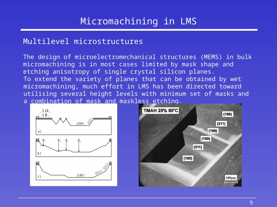
To extend the variety of planes that can be obtained by wet micromachining, much effort in LMS has been directed toward utilising several height levels with minimum set of masks and a combination of mask and maskless etching.
Si NSiO
3 4
2
(1 0 0 ) ( 111
)
(3 11 )
(111
)
(1 0 0 )
a)
b)
c)
d 1 d 2 d 3 d 4
Multilevel microstructures
The design of microelectromechanical structures (MEMS) in bulk micromachining is in most cases limited by mask shape and etching anisotropy of single crystal silicon planes.
10
Micromachining in LMS
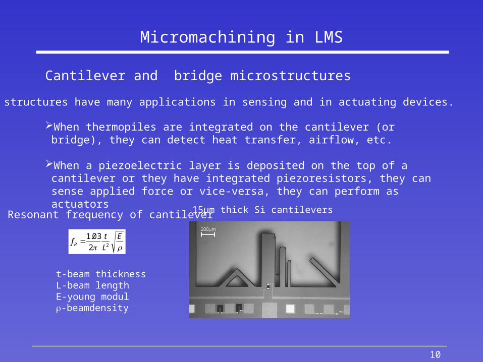
Cantilever and bridge microstructures
When thermopiles are integrated on the cantilever (or bridge), they can detect heat
transfer, airflow, etc.
When a piezoelectric layer is deposited on the top of a cantilever or they have integrated piezoresistors, they can sense applied force or vice-versa, they can perform as actuators
15µm thick Si cantilevers
E
L
tfR 22
03.1
Resonant frequency of cantilever
t-beam thicknessL-beam lengthE-young modul-beamdensity
These structures have many applications in sensing and in actuating devices.
11
Micromachining in LMS
Cantilever and bridge microstructures
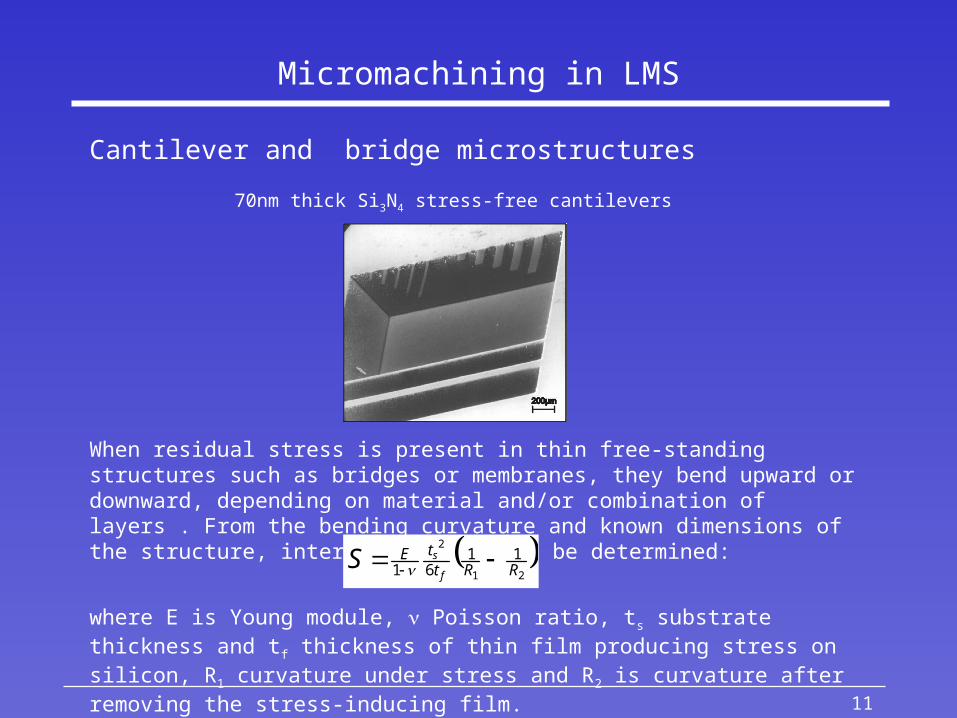
70nm thick Si3N4 stress-free cantilevers
When residual stress is present in thin free-standing structures such as bridges or membranes, they bend upward or downward, depending on material and/or combination of layers . From the bending curvature and known dimensions of the structure, internal stress S can be determined:
where E is Young module, Poisson ratio, ts substrate thickness and tf thickness of thin film producing stress on silicon, R1 curvature under stress and R2 is curvature after removing the stress-inducing film.
21
211
61 RRttE
f
sS

12
Micromachining in LMS
Aluminum cantilevers
Aluminum can play an important role as a masking material in anisotropic etching (usually 5% TMAH-water+1.5% dissolved Si+0,6% ammonium peroxodisulfate). By underetching method, cantilevers are obtained.
Aluminum cantilevers were fabricated by above procedure (100µm long, 10µm wide,0.45µm thick):

13
Micromachining in LMS
Micromachined accelerometer structure with piezoresisitive sensing
Top view
Bottom view
Inertial mass is suspended on three hinges. Central one has integrated sensing piezoresistor, while other two make the device more robust against accelerations in other directions.
Cross-section
Under the acceleration inertial mass is displaced with respect to the fixed part of microstructure, causing thereby stress in the piezoresistor located in the central hinge. This results in proportional resistance change, which is detected by the outer electric circuitry.
The accelerometer microstructure was realised entirely by wet etching processes.

14
Micromachining in LMS
Optical fibre aligning grooves
For precise alignment of optical fibres in case of positioning or interconnections on microoptical benches, where light sources or detection systems can be realised monolithically, microstructures such as grooves are useful. By aid of wet or/and dry etching techniques, different groove structures can be obtained.
<110> <110> <100>
Telecommunications and optical applications
Microstructures found various applications also in these fields as single optical components for interconnections between fibres and other active devices, optical benches, passive or active reflecting mirrors, active switches, beam splitters, etc.
15
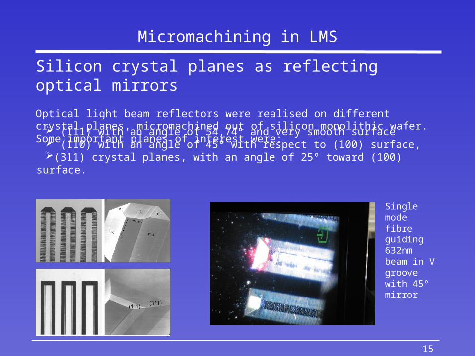
Micromachining in LMS
(111) with an angle of 54,74º and very smooth surface (110) with an angle of 45º with respect to (100) surface, (311) crystal planes, with an angle of 25º toward (100) surface.
Single mode fibre guiding 632nm beam in V groove with 45º mirror
Silicon crystal planes as reflecting optical mirrors
Optical light beam reflectors were realised on different crystal planes, micromachined out of silicon monolithic wafer. Some important planes of interest were:

16
Micromachining in LMS
{110} {111} {212} {311}
x
yIsc
slit
photodiode
Reflected beam angles depending on micromachined crystal planes:
Measurements of reflected angles and dispersion of reflected light were performed by photodiode response.Average surface roughness Ra is in the range of 25nm and the lowest scattering was obtained with (111) crystal planes (cca. 3º)
X direction [µm]
-5 0 5 10 15 20 25 30 35
Isc [µ
A]
0
200
400
600
40º17º20º
Single mode fibre-NA=0.1

17
Micromachining in LMS
l ig h t s o u rc e= 6 3 2 n m ,= 1 ,3 3 µ m
s in g le m o d e fib re
x y z s ta g ex y z s ta g e
re fle c te d im a g e o ns e m itra n s p a re n ts c re e n
x y z s ta g e
c o llim a to r
s a m p le
Characterisation setup of reflecting mirror planesby beam image dispersion
K OH (100)<110> Al K OH-IPA (100)<100> A l K OH-IPA (100)<100>
TM A H (100)<110>A lTM A H (100)<110>
K OH-IPA (100)<110>
TM A H-IPA (100)<110>A l TM A H (110)<010>
Results:
Beam reflecting images from crystal planes preparedwith different etchants: Image shape is proportional to the crystal plane roughness

18
Micromachining in LMS
surface preparation - to obtain particle- free and hydrophilic surface. Cleaning of silicon surface has a great impact on surface chemistry and topography.
hydrophilic surface <10ºafter forming hydrous chemical oxide
hydrophobic surface >50ºafter RCA cleaning
AFM after RCARa=10-12nm
Low temperature bonding of silicon wafers (<400ºC)
In order to bond wafers successfully attention was paid to the following steps:
After RCA cleaning dry wafers were immersed into hot nitric acid (HNO3), allowing growth
of a few monolayers of fresh hydrous chemical oxide, increasing roughness to Ra=10-12nm.

19
Micromachining in LMS
By doing this, we actually help to accommodate the two surfaces that suffer from nonflatness, through elastic deformation process via attractive Van der Waals forces.
a)
b)
c)
Si
Mating of rough surfaces via elastic deformation (zip)
SiH
H
HH
HH
HH
HO
HO HOHOHO HO
H O H O H O H O H
active wafer
support w afer
1.10 H/cm14 2
2.10 O/cm15 2
5.10 H/cm13 2
2-3.10 H O/cm15 22
1-2.10 OH/cm15 2
Bond interface chemistry
interface between two wafers
prebonding at room temperature - two wafers were put into intimate contact in cleanroom ambient at room temperature. We initiate bonding by locally pressing the centre region from the top, thus enabling bonding phenomenon to propagate radially.

20
Micromachining in LMS
bond annealing (strengthening) - transformation of silanol to strong siloxane bonds takes place at elevated temperature. Bond strengthening was performed in the range from 80C to 400C, in different ambients. Bonding efficiency was characterised by quantitative analysis of tensile strength of bond.
Overall reaction across two hydrophilic surfaces:
Si-OH + OH-SiSi-O-Si +H2O
covalent bonds

21
Micromachining in LMS
Bond quality characterisation
Voids at the bonding interface reduce the bond strength. Their origin could be trapped ambient gas, particle or gaseous by-product from interface reaction.
Bondinginterface
Cross-section of bonded interface
Void
Voids
IR transmission investigation is performed by IR camera, model PTC-10A. By this method only larger area defects can be recognised.
Voids

22
Micromachining in LMS
Differential pressure sensor
Four p-type resistors are diffused into the silicon membrane and connected in the Wheatstone bridge configuration. Membrane is realised by bulk micromachining in 33% KOH etchant at 80ºC and has thickness of 232µm.
Silicon thin membrane (25µm)
Diffused piezoresistors

23
Micromachining in LMS
Differential pressure sensor characteristics
O p e ra tin g P re s su re R a n g e .. .. .. .. .. .. . .. .. .. .. .. .. .. .. .. .. .. .. .. .. .. .. .. .. .. .. 0 .. 1 B a rO v e rp re ss u re (m in ) .. .. .. .. .. .. .. .. . .. .. .. .. .. .. .. .. .. .. .. .. .. .. .. .. .. .. .. .. .. .. .. .. .. .. . 5 B a rS u p p ly C u rre n t .. .. .. .. .. .. .. .. .. .. .. .. .. .. .. .. .. .. .. .. .. .. .. .. .. .. . .. .. .. .. .. .. .. .. .. 1 .. 5 m AO p e ra tin g Te m p e ra tu re R a n g e .. .. .. .. .. .. .. .. .. .. .. .. .. .. .. .. .. .. .. . - 4 0 .. + 1 2 0 ° CS to ra g e Te m p e ra tu re R a n g e . .. .. .. .. .. .. .. .. .. .. .. .. .. .. . .. .. .. .. .. .. . - 4 0 . . + 1 2 0 ° CD im e n s io n s (W /L /H ) . .. .. .. .. .. .. .. .. .. .. .. .. .. .. .. .. .. . .. .. .. .. . 1 9 5 0 /1 9 5 0 /3 8 5 µ mIn p u t R e s is ta n c e .. .. .. .. .. .. .. .. .. .. .. .. .. .. .. .. .. .. .. .. .. .. .. .. .. .. .. .. . . 3 9 0 . . 4 3 0 o h m sO u tp u t R e s is ta n c e .. .. . .. .. .. .. .. .. .. .. .. .. .. .. .. .. .. .. .. .. .. .. .. .. .. .. .. 3 9 0 .. 4 3 0 o h m sS e n s it iv ity .. .. .. .. .. .. .. .. .. .. .. .. .. .. .. .. .. .. .. .. .. .. .. .. .. .. .. .. .. . .. .. .. .. .. .. . 3 0 m V /V /B a rO ffse t Vo lta g e a t Z e ro P re s su re (m a x .) . .. .. .. .. .. .. .. .. .. .. .. .. .. .. .. .. .. . 5 m V /VTe m p e ra tu re C o e ff . o f R e s is ta n c e . .. .. .. .. .. .. .. .. .. .. .. .. .. . .. .. .. .. .. . 0 ,5 o h m /° CTe m p e ra tu re C o e ff . o f O ffs e t Vo l ta g e (m a x .) . .. .. .. .. .. .. .. .. . 0 ,2 m m H g /° CO ffse t R e p e a ta b il i ty .. .. .. .. . .. .. .. .. .. .. .. .. .. .. .. .. .. .. .. .. .. .. .. .. .. .. .. .. .. ± 0 ,1 m m H gS p a n R e p e a ta b il ity .. .. .. .. .. .. .. .. . .. .. .. .. .. .. .. .. .. .. .. .. .. .. .. .. .. .. .. .. .. .. . ± 0 ,3 m m H gL o n g Te rm S ta b il i ty o f O ffs e t a n d S e n s itiv ity .. .. .. .. .. .. .. .. .. .. ± 0 ,3 m m H gA lu m in iu m M e ta liz a tio nR e la tiv e P re ss u re S e n s o r
C H A R A C T E R IS T IC S
24
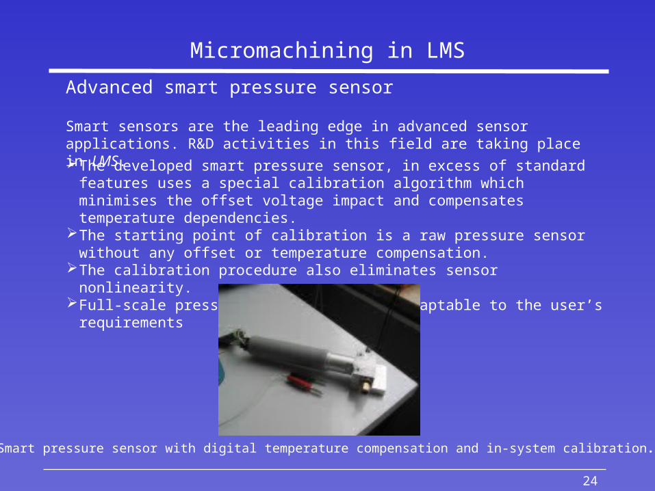
Micromachining in LMS
The developed smart pressure sensor, in excess of standard features uses a special calibration algorithm which minimises the offset voltage impact and compensates temperature dependencies.
The starting point of calibration is a raw pressure sensor without any offset or temperature compensation.
The calibration procedure also eliminates sensor nonlinearity.Full-scale pressure range is totally adaptable to the user’s requirements
Smart pressure sensor with digital temperature compensation and in-system calibration .
Advanced smart pressure sensor
Smart sensors are the leading edge in advanced sensor applications. R&D activities in this field are taking place in LMS.

25
Laboratory of Microsensor Structures and Electronics (LMSE)Phone: (+386 1) 4768 303Fax: (+386 1) 4264 630http://paris.fe.uni-lj.si/lms/
Head: Professor Dr. Slavko Amon
Staff: E-mail: Ext:Professor Dr. Slavko Amon [email protected] 352Professor Dr. Igor Medič [email protected] 326Assistant Professor Dr. Žarko Gorup [email protected] 325Assistant Professor Dr. Andrej Levstek [email protected] 846Assistant Professor Dr. Drago Resnik [email protected] 303Assistant Professor Dr. Danilo Vrtačnik [email protected] 303Senior Lecturer Niko Basarič, M. Sc. [email protected] 331Researcher Uroš Aljančič, M. Sc. [email protected] 303Researcher Matej Možek, M. Sc [email protected] 303Technical Collaborator Matjaž Cvar [email protected] 303Technical Collaborator Marijan Žurga [email protected] 276Phone: (+386 1) 4768 + Ext.


