1 May 2008 2006 by Fabian Kung Wai Lee 1 8D - General Single-Stage Small-Signal Amplifier Design The information in this work has been obtained from sources believed to be reliable. The author does not guarantee the accuracy or completeness of any information presented herein, and shall not be responsible for any errors, omissions or damages as a result of the use of this information. May 2008 2006 by Fabian Kung Wai Lee 2 1.0 General Single-Stage Small-Signal Amplifier Design Procedures
Transcript
1
May 2008 2006 by Fabian Kung Wai Lee 1
8D - General Single-Stage
Small-Signal Amplifier
Design
The information in this work has been obtained from sources believed to be reliable.The author does not guarantee the accuracy or completeness of any informationpresented herein, and shall not be responsible for any errors, omissions or damagesas a result of the use of this information.
May 2008 2006 by Fabian Kung Wai Lee 2
1.0 General Single-Stage
Small-Signal Amplifier
Design Procedures
2
May 2008 2006 by Fabian Kung Wai Lee 3
Practical Single-Stage Small-Signal
Amplifier Design (1)
• Thus far we have considered different aspects of small-signal amplifier
design.
• We have look at stability analysis and simultaneous conjugate match
for maximum power gain under unconditionally stable case.
• Using Constant GP Circle to determine ΓL for conditionally stable
amplifier, or when we do not require maximum power gain.
• Plotting Constant Noise Figure Circle to optimize Γs for optimum noise
performance.
• Plotting Input Mismatch Circle to optimize for VSWRin and to set the
actual transducer power gain (in collaboration of Constant Gp Circle).
• A general single-stage amplifier can be designed to meet multiple
parameters, e.g. power gain, bandwidth, noise figure, input and output
mismatch.
May 2008 2006 by Fabian Kung Wai Lee 4
Practical Single-Stage Small-Signal
Amplifier Design (2)
• Unfortunately these parameters compete with each other in determining
the required load and source impedance value.
• For instance, when we want to maximize power gain, we usually have
to sacrifice stability and noise performance.
• When we desire low noise figure, we have to trade off with moderate
input mismatch and lower power gain.
• In designing an amplifier, we use various circles learnt in the previous
sections to help us to balance the trade-off carefully.
• After finding the optimum load and source reflection coefficients,
impedance transformation is usually employed to map the actual
load/source impedance to the desired value.
• Computer-aided design is often compulsory for optimum design.
3
May 2008 2006 by Fabian Kung Wai Lee 5
Practical Single-Stage Small-Signal
Amplifier Design (3)
ZL
ZcZc
ZsVs
VSWRinVSWRout
PA PL
GTF
Stability
Factor Bandwidth
May 2008 2006 by Fabian Kung Wai Lee 6
Single-Stage Small-Signal Amplifier
Design Flow
SCM
Start
Set frequency range
Set VSWR1
Set NF
Set GT or GP
Get S-parameters
Design DC biasing,
choose components.
Check for stability
Find Γsm and ΓLm
Find GP(max)
Design impedance
transformation network
Final verification usingsimulation software
Draw GP circles
Draw Input mismatchcircleDraw F circle
Find ΓL
Done
Find Γs
Meet Requirement
Not Meet
RequirementA B
LNA/
non-SCM
A
B
Not Meet Requirement
4
May 2008 2006 by Fabian Kung Wai Lee 7
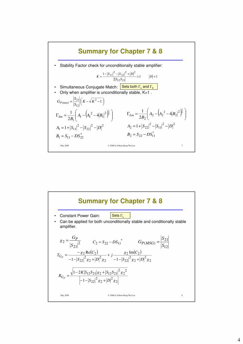
Summary for Chapter 7 & 8
−−= 12
12
21(max) KK
S
SGP
( )
*22111
2222
2111
21
211
1
1
42
1 21
DSSB
DSSA
BAAB
Sm
−=
−−+=
−−=Γ ( )
*11222
2211
2222
22
222
2
1
42
1 21
DSSB
DSSA
BAAB
Lm
−=
−−+=
−−=Γ
• Stability Factor check for unconditionally stable amplifier:
• Simultaneous Conjugate Match:
• Only when amplifier is unconditionally stable, K>1 .
1 12
1
2112
2222
211
<>+−−
= DSS
DSSK
Sets both ΓL and Γs
May 2008 2006 by Fabian Kung Wai Lee 8
Summary for Chapter 7 & 8
• Constant Power Gain:
• Can be applied for both unconditionally stable and conditionally stable
amplifier.
*11222 DSSC −=
( ) ( )
22
22
22
22
22
22
22
22
1
Im
1
Re
gDgS
Cgj
gDgS
CgT
PG+−−
++−−
−=
221
2S
Gg P=
22
22
22
22
2211222112
1
21
gDgS
gSSgSSKR
PG+−−
+−=
12
21)(
S
SG MSGP =
Sets ΓL
5
May 2008 2006 by Fabian Kung Wai Lee 9
Summary for Chapter 7 & 8
• Constant Noise Figure:
22mS
s
immS
s
im YY
G
RFZZ
R
GFF −+=−+=
( ) ( )
io
mm
e
mmoi
GZ
FF
R
FFZN
4
1
4
122
Γ+−=
Γ+−=
i
mFcenter
N+
Γ=Γ
1
i
mii
FradN
NN
R+
Γ−+
=1
122
Sets Γs
May 2008 2006 by Fabian Kung Wai Lee 10
Summary for Chapter 7 & 8
• Constant Input Mismatch:
( ) 211
*11
11 Γ−−
Γ=Γ
M
MScenter
( ) 211
211
11
11
Γ−−
Γ−−
=M
M
RSrad
PT GMG 1=2
1
21
2
11
11
s
sM
ΓΓ−
Γ−
Γ−
=
1
111
2
M-1-1
M-11VSWR 1
+==− Mρ
2
1
11
1
11
+
−−=
VSWR
VSWRM
Sets Γs
6
May 2008 2006 by Fabian Kung Wai Lee 11
Example 1 (Textbook)- General
Amplifier Design Example
• A BJT, biased at IC= 10mA, VCE= 6V is operated at f = 2.4GHz. The biasing network is shown in the next slide. The corresponding S-parameters are s11= 0.3<30o, s12= 0.2<-60o, s21= 2.5<-80o, s22= 0.2<-15o. The noise parameters of the BJT are Fm(dB)=1.7dB, Re=4Ω and Γm
= 0.5<45o. Assume Zo=50 Ω.
• Design a Low-Noise Amplifier using the BJT circuit, with:
– A power gain Gp of at least 8dB.
– Noise figure F less than 2.0dB.
– VSWR1 less than 2.0.
– The Amplifier has a source of 50 Ω and load of 50 Ω.
May 2008 2006 by Fabian Kung Wai Lee 12
D.C. Biasing Network
S11 = 0.3<30o = 0.260+j0.150
S12 = 0.2<-60o = 0.100-j0.173
S21 = 2.5<-80o = 0.434-j2.462
S22 = 0.2<-15o = 0.193-j0.052
Cc1
Cc2
L1
L2
CdRc
Vcc
Rb
Port 1
(input)
Port 2
(Output)
Ic = 10mA
6V
@ 2.4GHzSimulated S-parameters
7
May 2008 2006 by Fabian Kung Wai Lee 13
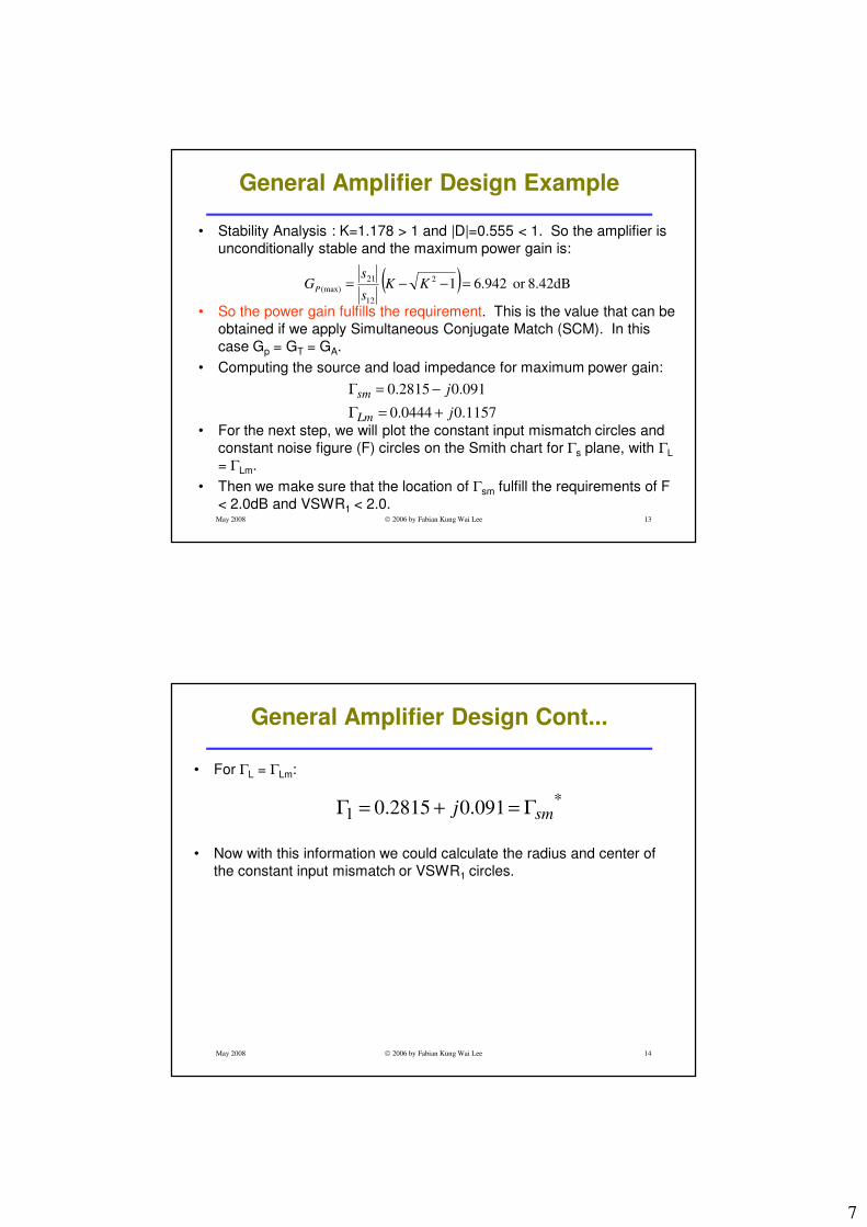
General Amplifier Design Example
• Stability Analysis : K=1.178 > 1 and |D|=0.555 < 1. So the amplifier is
unconditionally stable and the maximum power gain is:
• So the power gain fulfills the requirement. This is the value that can be
obtained if we apply Simultaneous Conjugate Match (SCM). In this
case Gp = GT = GA.
• Computing the source and load impedance for maximum power gain:
• For the next step, we will plot the constant input mismatch circles and
constant noise figure (F) circles on the Smith chart for Γs plane, with ΓL
= ΓLm.
• Then we make sure that the location of Γsm fulfill the requirements of F
< 2.0dB and VSWR1 < 2.0.
( ) 8.42dBor 942.612
12
21
(max) =−−= KKs
sGP
1157.00444.0
091.02815.0
j
j
Lm
sm
+=Γ
−=Γ
May 2008 2006 by Fabian Kung Wai Lee 14
General Amplifier Design Cont...
*1 091.02815.0 smj Γ=+=Γ
• For ΓL = ΓLm:
• Now with this information we could calculate the radius and center of
the constant input mismatch or VSWR1 circles.
8
May 2008 2006 by Fabian Kung Wai Lee 15
General Amplifier Design Cont...
Γs plane
Circles...VSWR1=2.0
Radius=0.3071
Tcenter=0.253-j0.082
VSWR1=1.8
Radius=0.262
Tcenter=0.260-j0.084
F=2.0dB (F=1.5849)
Radius=0.5772
Tcenter=0.215+j0.215
F=1.8dB (F=1.5136)
Radius=0.372
Tcenter=0.292+j0.292
Constant F
circle, F=2.0dB
Γm
Constant F
circle, F=1.8dB
VSWR1=2.0
Γsm
VSWR1=1.8
May 2008 2006 by Fabian Kung Wai Lee 16
General Amplifier Design Cont...
• From the previous slide, we see that all the requirements are fulfilled. So
the required source and load reflection coefficients are:
• Noting that Γsm is near the F=1.8dB Circle, the performance parameters
of the amplifier are:
Gp = 6.942 or 8.42dB.
VSWR1 = 1 or M = 1.
F ≅ 1.568 or 1.5136dB < 2.0dB.
• Finding the source and load impedance:
1157.00444.0
091.02815.0
j
j
Lm
sm
+=Γ
−=Γ
349.17982.861
1jZZ
sm
smos −=
Γ−
Γ+=
487.12134.531
1jZZ
Lm
LmoL +=
Γ−
Γ+=
9
May 2008 2006 by Fabian Kung Wai Lee 17
General Amplifier Design Cont...
• Since the original source and load impedance do not correspond
to these values, impedance transformation networks are used at
the input and output port of the amplifier.
• The final block diagram:
Amplifier50
2.99nH
0.80pF 50
Zsm ZLm
@ 2.4GHz
1.14nH
0.13pF
VSWR1 = 1
May 2008 2006 by Fabian Kung Wai Lee 18
Complete Schematic of the Example
Cc1
Cc2
L1
L2
CdRc
Vcc
Rb
2.99nH
0.8pF
1.14nH
0.13pFQ1 C2
L4
L3
C1
10
May 2008 2006 by Fabian Kung Wai Lee 19
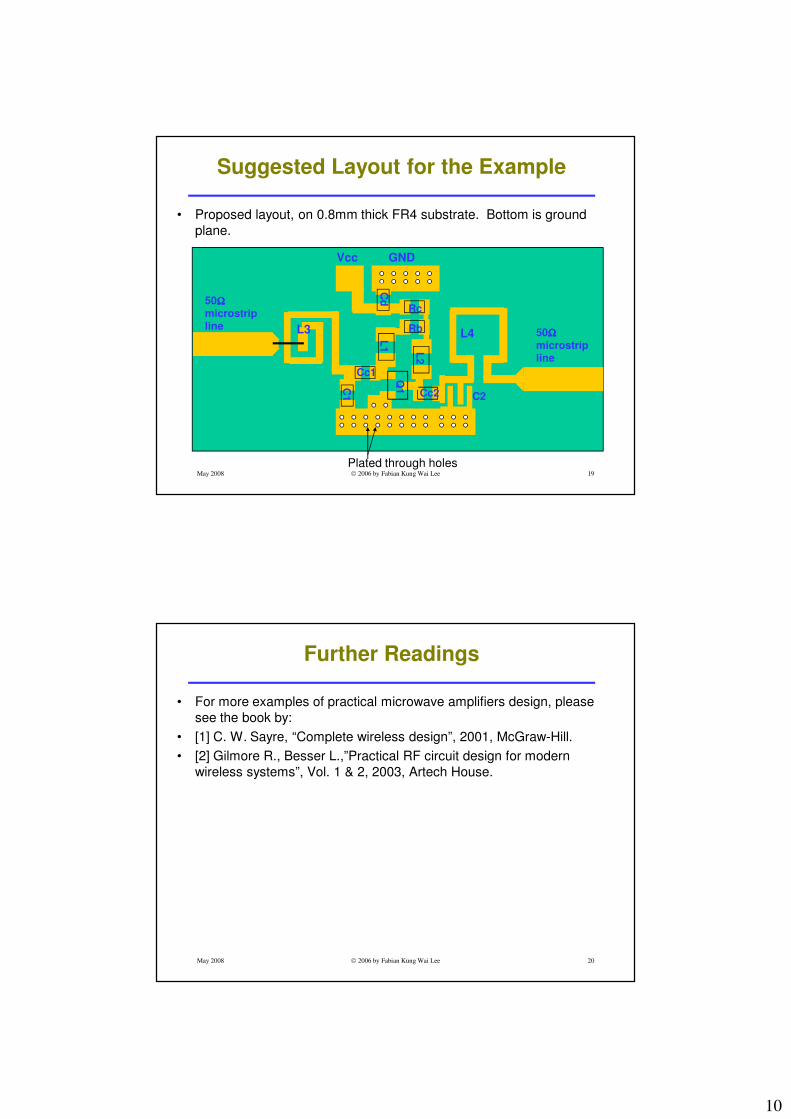
Suggested Layout for the Example
• Proposed layout, on 0.8mm thick FR4 substrate. Bottom is ground
plane.
Vcc GND
Cc2
Cc1
C1
Q1
L3 L4
C2
50ΩΩΩΩ
microstrip line
50ΩΩΩΩ
microstrip line
Rc
Cd
L1
L2
Rb
Plated through holes
May 2008 2006 by Fabian Kung Wai Lee 20
Further Readings
• For more examples of practical microwave amplifiers design, please
see the book by:
• [1] C. W. Sayre, “Complete wireless design”, 2001, McGraw-Hill.
• [2] Gilmore R., Besser L.,”Practical RF circuit design for modern
Small-signal requirement of Amplifer: NOTE: 1. Set a reasonable input mismatch factor "Minput" (between 0 to 1).2. Move marker m1 along constant Gp circles to obtainsuitable load impedance and m2 along the constant input mismatchcircle to obtain suitable source impedance.
Noise parameters:
May 2008 2006 by Fabian Kung Wai Lee 32
Input and Output Impedance
Transformation Network
The following LC networks are used:
1. Load Network: to transform ZL = 50 to 74+j57 (approximate) at 900MHz.
2. Source Network: to transform Zs = 50 to 28+j10 (approximate) at 900MHz.
Port
Load
Num=1
L
L1
R=
L=10.2 nHC
C1
C=0.68 pF
R
RL
R=50 Ohm
Port
Source
Num=1
L
L1
R=
L=6.16 nHC
C1
C=3.13 pF
R
Rs
R=50 Ohm
Load network Source network
17
May 2008 2006 by Fabian Kung Wai Lee 33
The Complete Schematic
L
Lm2
R=
L=2.2 nH
S_Param
SP1
NoiseOutputPort=2
NoiseInputPort=1
CalcNoise=yes
CalcZ=yes
Step=2.0 MHz
Stop=1600.0 MHz
Start=200 MHz
S-PARAMETERS
Term
Term2
Z=50 Ohm
Num=2
StabFact
StabFact1
K=stab_fact(S)
StabFact
L
Lm3
R=
L=10.0 nH
C
Cm2
C=0.68 pF
C
Cc2
C=100.0 pF
pb_phl_BFR92A_19921214
Q1
C
Cm1
C=3.3 pF
Term
Term1
Z=50 Ohm
Num=1
L
Lm1
R=
L=4.7 nH
C
Cc1
C=100.0 pF R
RB2
R=1.5 kOhm
R
RB1
R=1 kOhm
L
LC
R=
L=100.0 nH
R
RC
R=470 Ohm
V_DC
SRC1
Vdc=3.0 V
Practical L and C values are used to approximate the source and load