10W GaN effektforsterker med Envelope Tracking og optimalisert tilpasning Andreas Bognøy Master i elektronikk Hovedveileder: Morten Olavsbråten, IET Institutt for elektronikk og telekommunikasjon Innlevert: januar 2015 Norges teknisk-naturvitenskapelige universitet
Transcript
10W GaN effektforsterker med Envelope Tracking og optimalisert tilpasning
Andreas Bognøy
Master i elektronikk
Hovedveileder: Morten Olavsbråten, IET
Institutt for elektronikk og telekommunikasjon
Innlevert: januar 2015
Norges teknisk-naturvitenskapelige universitet
Summary
Modern communication standards are based on signals which exploit high peak-to-averagepower ratio, signals which force the power amplifiers (PA) to operate at power back offlarge amounts of the time, where efficiency is poor. As a result, power amplifiers becomean important component and advanced methods are being developed and improved in or-der to enhance efficiency. Among these methods is Envelope Tracking, a method where adynamic supply is used for reducing supplied power at backed off RF power levels.
This thesis presents the design and characterization of a class AB PA in order to investigateits behavior when used in an envelope tracking setup. Design was based around a 10 WCree general purpose GaN HEMT, and matching was done based on impedances foundfrom load pull techniques. In addition, a set of different criteria for the envelope trackinghas been investigated, showing varying results in terms of improvement and requirements.
Under fixed 28 V supply the PA showed a peak output power of 41.7 dBm at 2.4 GHz, hav-ing a 1 dB compression point at 41.0 dBm output power. A small signal gain of 14.1 dBwas measured, and at the onset of compression the PA showed 12.2 dB gain. At peakoutput power, the measured power-added efficiency was 68.2 %. The PA also featured anundesired high-gain band from 2.4 GHz and all the way down to 100 MHz.
To estimate the envelope tracking performance, the PA was measured at reduced supplyvoltages, which were analyzed in Matlab. For 5-6 dB back off, improvements rangingfrom 2 % to 17 % could be achieved by adding envelope tracking, however reducing thegain as low as below 8 dB. The resulting performance was also compared to cases wherea square supply function was applied, showing slight efficiency deterioration, but reducingthe bandwidth requirement of the dynamic supply this could possibly serve as a goodalternative as the envelope amplifier will operating with higher efficiency.
i
Sammendrag
Moderne kommunikasjonstandarder er basert pa signaler som drar nytte av høy peak-to-average effektforhold, signaler som tvinger effektforsterkere (PA) til a operere i back-offstore deler av tiden, hvor effektiviteten er lav. Som resultat, blir effektforsterkere viktigekomponenter og avanserte metoder utvikles og forbedres for a kunne øke effektiviteten.Blant disse metodene finner man envelope tracking, en metode hvor en dynamisk effekt-forsyning brukes til a redusere forsyningsspenning ved RF back-off.
Denne oppgaven presenterer konstruksjon og karakterisering av en klasse AB effektforsterker,for a undersøke ytelsen nar den brukes i et envelope tracking oppsett. Konstruksjonen varbasert rundt en 10 W Cree general purpose GaN HEMT og matchingen ble utført basert paimpedans som ble funnet ved hjelp av load pull teknikk. I tillegg har et sett med ulike kri-terier for Envelope Tracking blitt undersøkt med ulike resultater nar det gjelder forbedringog krav.
Under fast 28 V-tilførsel fikk effektforsterkeren en maksimal utgangseffekt pa 41,7 dBmved 2,4 GHz, med et 1 dB kompresjonspunkt for 41,0 dBm utgangseffekt. Det ble malt en sma signalforsterkning pa 14,1 dB og ved starten av kompresjon malte forsterkerenen effektforsterkning pa 12,2 dB. Ved maksimal utgangseffekt, var den malte PAE virkn-ingsgrad pa 68,2 %. Effektforsterkeren ga ogsa et uønsket band med høy forsterkning fra2,4 GHz og helt ned til 100 MHz.
For a estimere ytelsen for envelope tracking, ble effektforsterkeren malt med reduserteforsyningsspenninger, som ble analysert i Matlab. For back-off pa 5-6 dB, ble det oppnaddforbedringer mellom 2 % og 17 % nar det ble lagt til envelope tracking, men forsterknin-gen ble imidlertid redusert til sa lite som under 8 dB. Den resulterende ytelsen ble ogsasammenlignet med tilfeller der en kvadratisk supply funksjon ble brukt, med en svak re-duksjon i effektivitet som resultat. Ved a redusere bandbreddekravet for den dynamisketilførselen, kan dette imidlertid være et godt alternativ til konvensjonell envelope trackingmed lineær tracker.
ii
Preface
This thesis is submitted in fulfillment of the requirements for the degree of master of sci-ence (MSc) at the Department of Electronics and Telecommunications, Norwegian Univer-sity of Science and Technology (NTNU) and the work was carried out between september2014 and january 2015.
I would like to than my supervisor, associate professor Morten Olavsbraten, for giving methe chance to work in this promising and exciting field. His feedback and guidance alongthis project has been of great value to me and for that I am grateful. I would also like tothank the Elpro lab for fabrication of the microstrip design. Last but not least, I would liketo thank my friends and family for their never-ending motivation and encouragement.
Trondheim, Norway, January 2015Andreas Bognøy
iii
iv
Contents
Summary i
Preface iii
Table of Contents vi
List of Tables vii
List of Figures xi
Abbreviations xii
1 Introduction 1
2 Basic Theory 32.1 Transmission Line Theory and Wave Propagation . . . . . . . . . . . . . 3
5.2 Complete list of measured parameters under static operation. . . . . . . . 52
vii
viii
List of Figures
1.1 Technology development of RF PAs, figure from [1]. . . . . . . . . . . . 2
2.1 Lumped component equivalent of transmission line. . . . . . . . . . . . . 32.2 Cross section of microstrip transmission line, showing geometry (a) and
electromagnetic fields (b). Excerpt from [2]. . . . . . . . . . . . . . . . . 52.3 Output stability circles showing the stable area where |Γ| < 1 and unstable
areas where |Γ| > 1 for S11 both larger and smaller than unity. . . . . . . 82.4 RC high pass configuration used for stabilization at low frequencies. . . . 92.5 High abstraction level example of transmitter. . . . . . . . . . . . . . . . 102.6 Example system overview of transistor PA. . . . . . . . . . . . . . . . . 102.7 Example HEMT PA without matching networks, showing RF-ports, vin
and vout and DC-ports, Vg and Vd. . . . . . . . . . . . . . . . . . . . . . 112.8 Example of sine wave with compressed equivalent. . . . . . . . . . . . . 132.9 Output power showing 1dB compression point. . . . . . . . . . . . . . . 142.10 Output spectrum of two-tone input, showing harmonics and IMD-products.
The in-band products are marked. . . . . . . . . . . . . . . . . . . . . . 152.11 Gain as function of input power, showing the compression of the gain and
P1 dB. . . . . . . . . . . . . . . . . . . . . . . . . . . . . . . . . . . . . 152.12 IV curves for FET transistor with operating points for amplifier classes A-C. 162.13 Output power versus input power for gain matched (solid curve) and power
match (dotted curve). . . . . . . . . . . . . . . . . . . . . . . . . . . . . 182.14 Cross section of GaN HEMT, figure from [1]. . . . . . . . . . . . . . . . 192.15 Kahn technique, excerpt from [3]. . . . . . . . . . . . . . . . . . . . . . 202.16 PA with envelope tracking power supply. . . . . . . . . . . . . . . . . . . 202.17 Comparison of thermally dissipated power for fixed supply PA and ET PA. 212.18 Efficiency of ET PA as a function of back off from maximum power. . . . 222.19 PAE for PA for various supply voltage levels and ET trajectory and output
power PDF histogram. . . . . . . . . . . . . . . . . . . . . . . . . . . . 242.20 Examples of Rayleigh probability density functions (PDF). . . . . . . . . 242.21 Supply modulator transfer function for (a) efficiency and (b) linearity. . . 27
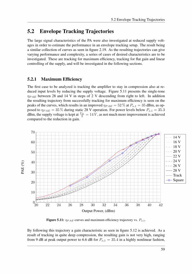
5.1 Single-tone output power characteristics. . . . . . . . . . . . . . . . . . . 535.2 Single tone available gain as function of output power. . . . . . . . . . . 535.3 single-tone a ηPAE as function of output power. . . . . . . . . . . . . . . 545.4 Measured two-tone output power vs. input power. . . . . . . . . . . . . . 555.5 Measured two-tone available gain vs. Po 2 . . . . . . . . . . . . . . . . . 555.6 Measured two-tone ηPAE vs. Po 2 . . . . . . . . . . . . . . . . . . . . . 565.7 Measured 3rd order IMD vs. Po 2 . . . . . . . . . . . . . . . . . . . . . 565.8 Measured S11 and S22 in smith chart. . . . . . . . . . . . . . . . . . . . 575.9 Measured |S21| for complete design. . . . . . . . . . . . . . . . . . . . 585.10 Measured |S12| for complete design. . . . . . . . . . . . . . . . . . . . 585.11 ηPAE-curves and maximum efficiency trajectory vs. Po 1. . . . . . . . . 595.12 GA-curves and maximum efficiency trajectory vs. Po 1. . . . . . . . . . . 605.13 Po 1-curves and maximum efficiency trajectory vs. Pi 1. . . . . . . . . . 615.14 Drain voltage vs. PA output (a) and input (b) voltage for maximum effi-
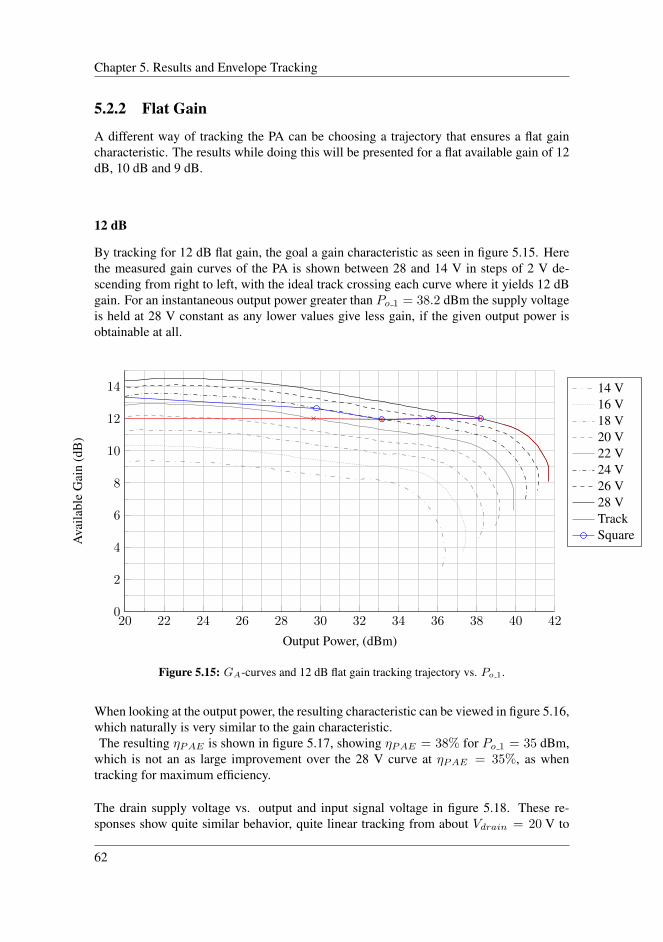
ciency tracking. . . . . . . . . . . . . . . . . . . . . . . . . . . . . . . . 615.15 GA-curves and 12 dB flat gain tracking trajectory vs. Po 1. . . . . . . . . 625.16 Po 1-curves and 12 dB flat gain tracking trajectory vs. Pi 1. . . . . . . . . 635.17 ηPAE-curves and 12 dB flat gain tracking trajectory vs. Po 1. . . . . . . . 635.18 Drain voltage vs. PA output (a) and input (b) voltage for 12 dB flat gain
tracking. . . . . . . . . . . . . . . . . . . . . . . . . . . . . . . . . . . . 645.19 GA-curves and 10 dB flat gain tracking trajectory vs. Po 1. . . . . . . . . 655.20 Po 1-curves and 10 dB flat gain tracking trajectory vs. Pi 1. . . . . . . . . 66
x
5.21 ηPAE-curves and 10 dB flat gain tracking trajectory vs. Po 1. . . . . . . . 665.22 Drain voltage vs. PA output (a) and input (b) voltage for 10 dB flat gain
tracking. . . . . . . . . . . . . . . . . . . . . . . . . . . . . . . . . . . . 675.23 GA-curves and 9 dB flat gain tracking trajectory vs. Po 1. . . . . . . . . . 685.24 Po 1-curves and 9 dB flat gain tracking trajectory vs. Pi 1. . . . . . . . . 695.25 ηPAE-curves and 9 dB flat gain tracking trajectory vs. Po 1. . . . . . . . 695.26 Drain voltage vs. PA output (a) and input (b) voltage for 9 dB flat gain
tracking. . . . . . . . . . . . . . . . . . . . . . . . . . . . . . . . . . . . 705.27 Drain voltage vs. PA output (a) and input (b) voltage for linear VD tracking. 715.28 GA-curves and linear VD tracking trajectory vs. Po 1. . . . . . . . . . . . 725.29 Po 1-curves and linear VD tracking trajectory vs. Pi 1. . . . . . . . . . . . 725.30 ηPAE-curves and linear VD tracking trajectory vs. Po 1. . . . . . . . . . . 73
6.1 Comparison between simulated and measured |S21|, and 1 dB bandwidths. 756.2 Comparison of ηPAE vs. Po 1 for different tracking cases. . . . . . . . . 786.3 Comparison of GA vs. Po 1 for different tracking cases. . . . . . . . . . . 796.4 Comparison of VS vs. Vin for different tracking cases. . . . . . . . . . . 79
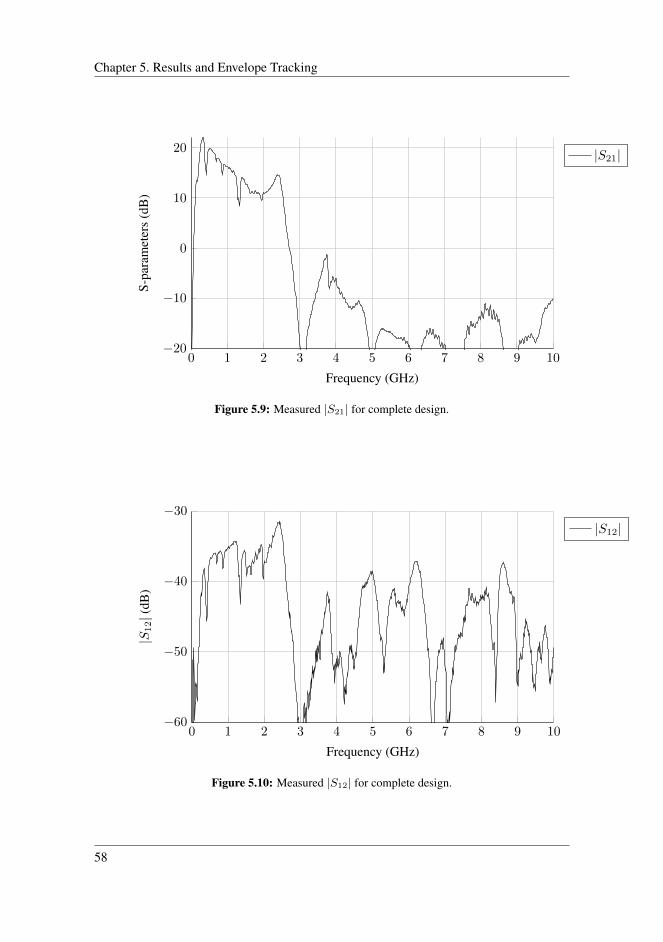
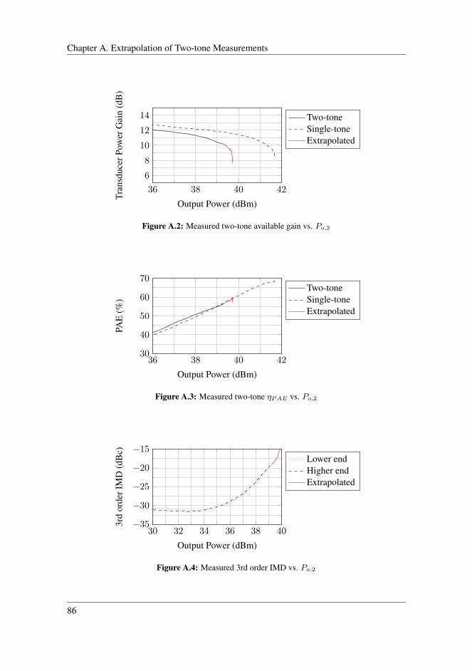
A.1 Measured two-tone output power vs. input power. . . . . . . . . . . . . . 85A.2 Measured two-tone available gain vs. Po 2 . . . . . . . . . . . . . . . . . 86A.3 Measured two-tone ηPAE vs. Po 2 . . . . . . . . . . . . . . . . . . . . . 86A.4 Measured 3rd order IMD vs. Po 2 . . . . . . . . . . . . . . . . . . . . . 86
ADS = Advanced Design SystemsCAD = Computer Aided DesignCMOS = Complementary Metal Oxide SemiconductorCW = Continuous WaveDPD = Digital PredistortionDSP = Digital Signal ProcessorDUT = Device Under TestEA = Envelope AmplifierEER = Envelope Elimination and RestorationET = Envelope TrackingFET = Field Effect TransistorGaAs = Gallium ArsenideGaN = Gallium NitrideHB = Harmonic BalanceHBT = Heterojunction Bipolar TransistorHEMT = High Electron Mobility TransistorHFET = Heterojunction Field Effect TransistorIMD = Intermodulation DistortionIMN = Input Matching NetworkLDMOS = Laterally Diffused Metal Oxide SemiconductorMMIC = Monolithic Microwave Integrated CircuitMOSFET = Metal Oxide Semiconductor Field Effect TransistorOMN = Output Matching NetworkPA = Power AmplifierPAE = Power-Added EfficiencyPCB = Printed Circuit BoardPAPR = Peak-to-Average Power RatioRF = Radio FrequencyRFPA = Radio Frequency Power AmplifierRL = Return LossSi = SiliconSiGe = Silicon GermaniumSM = Supply ModulatorSMC = Surface Mounted ComponentVNA = Vector Network AnalyzerVSA = Vector Signal AnalyzerVSG = Vector Signal Generator
xii
Chapter 1Introduction
Wireless technology is getting more widespread by the minute. The need to be availableanytime and anywhere is a problem both introduced and solved by wireless electronic de-vices. Especially the greatly increased use of handheld devices has increased the focuson research and development of wireless technology. Data rates can not seem to get largeenough and quality of service constantly seem to be an issue among users. As a result,more complex signal forms emerge to increase the data rate and allow a larger numberof subscribers to communicate simultaneously, making it harder to develop adequate RFelectronics.
A limiting component in the RF output stage of transmitters is the power amplifier (PA).Among the required characteristics for the PA is good linearity, high gain and efficientoperation, all which trade off against each other [1]. In a mobile handset, the PA is alsoone of the components which use the most power, and with the modern communicationstandards, which exhibit high peak-to-average power ratio (PAPR), the PA efficiency isdecreased. Improvement of the PA efficiency is thus focused on as a way of improving thebattery lifetime of mobile handsets and provides an advantage for electronics manufactur-ers.
Improvement of the PA efficiency is also beneficial for static transmitters, such as directradio links, satellite links and, perhaps most notably, mobile carriers who operate a largenumber of base stations. Improved efficiency can therefore result in greatly reduced powerexpenses. A lot of research has therefore been conducted, resulting in development ofadvanced methods for improving the efficiency of PAs, allowing PAPR increase, as seenin figure 1.1.Modern high power transmitters are often based on GaN HEMT transistor technology. TheHEMT fields high current densities and allows high voltages, resulting in high gain andhigh power for a small device. Along with high saturated electron velocity, making it ableto operate at relatively high frequencies. This makes the HEMT ideal for high power PAsand promising for the current most promising efficiency improvement technique, envelopetracking, a technique that improves efficiency for modern high-PAPR signals.
1
Chapter 1. Introduction
Figure 1.1: Technology development of RF PAs, figure from [1].
Envelope tracking is showing potential to become a method which can significantly im-prove efficiency while not necessarily deteriorating linearity of PAs too much. The basicconcept of envelope tracking is to dynamically reduce the supplied power as output RFpower is reduced by shaping the supply signal from the envelope of the RF signal. Thisresults in the PA operating in, or closer to the highly efficient compression area for a widerdynamic range of output power.
This thesis presents the design and performance of a class AB GaN HEMT PA using Ag-ilent ADS CAD software. The input and output matching networks have been optimizedfor high efficiency using source and load pull techniques. Fabrication was done in mi-crostrip, and the PA characteristics were measured for fixed and reduced supply levels,which were then analyzed in Matlab for estimating the characteristics of the PA when uti-lizing envelope tracking. The specifications for the PA that were to be met are listed intable 1.1.
Table 1.1: Specifications for PA.
Parameter Specified valueFrequency 2.4 GHzBandwidth (1 dB) > 100 MHzGain > 12dBOutput Power > 40 dBm|S11| [dB] < −10 dB
2
Chapter 2Basic Theory
2.1 Transmission Line Theory and Wave PropagationWhen analyzing circuits using alternating currents and voltages, transmission line theoryis not required provided that the wavelengths are substantially greater than the physicaldimensions of a network. If the dimensions of the network equal a considerable fractionof a wavelength or more, transmission line theory needs to be considered [4].
+
v(z, t)
R∆z L∆z
−
G∆z C∆z
+
−
v(z + ∆z, t)
i(z, t) i(z + ∆z, t)
Figure 2.1: Lumped component equivalent of transmission line.
In this case, the transmission lines are considered distributed elements, where voltages andcurrents may vary in amplitude and phase over the length of the line. These waves are de-scribed by a pair of first-order partial differential equations called telegrapher’s equations[5]. For sinusoidal steady-state conditions these can be solved, yielding the time-harmonicone-dimensional Helmholtz equations,
d2V (z)
dz2− γ2V (z) = 0 (2.1)
d2I(z)
dz2− γ2I(z) = 0 (2.2)
for the voltage and current phasors V (z) and I(z) of position z along the line, where
3
Chapter 2. Basic Theory
γ = α+ jβ =√
(R+ jωL)(G+ jωC) [m−1] (2.3)
is the propagation constant composed of an attenuation constant, α, and phase constant,β. The propagation constant is also dependent on the angular frequency, ω [rad/s] and thetransmission line parameters explained in table 2.1. Solutions to (2.1) and (2.2) yield the
Table 2.1: Parameter descriptions.
Parameter DescriptionR Resistance per unit length in Ω/mL Inductance per unit length in H/mG Conductance per unit length in S/mC Capacitance per unit length in C/m
traveling wave solutionsV (z) = V +
0 e−γz + V −0 e
γz (2.4)
I(z) = I+0 e−γz + I−0 e
γz (2.5)
where the plus and minus superscripts denote wave amplitudes traveling in the positiveand negative z direction respectively. The exponential factors are representing the corre-sponding waves, such that e−γz gives a forward traveling wave, and eγz give a backwardtraveling wave along the length of the line, z.
The characteristic impedance of the transmission line is defined as
Z0 =V +0
I+0= −V
−0
I−0=
√R+ jωL
G+ jωC(2.6)
When terminating a transmission line with an arbitrary load impedance, ZL, there may bea reflection of the incident wave, which is described by the voltage reflection coefficient,
Γ =V −0V +0
=ZL − Z0
ZL + Z0(2.7)
For a fully passive network, Γ is a complex number with |Γ| ∈ [0, 1], indicating the ratio ofthe incident wave, V +
0 , which is reflected as V −0 . To obtain Γ = 0 the load impedance ZLmust be equal to the characteristic impedance, Z0, otherwise a return loss is experienced,defined as
RL [dB] = −20 log |Γ| (2.8)
for |Γ| given in (2.7) so that a matched load(Γ = 0) has a return loss of −∞ [dB] and atotal reflection (|Γ| = 1) gives RL = 0 [dB].
The length of a transmission line is often expressed as an electric length, θ = βl, whichis the phase of a signal propagated along a line of length l. The input impedance of atransmission line of length l and terminated by ZL, is given as
Zin = Z0ZL + Z0 tanh γl
Z0 + ZL tanh γl(2.9)
4
2.1 Transmission Line Theory and Wave Propagation
which yields two interesting special cases.
Zin =Z20
ZL(2.10)
for l = λ4 and
Zin = Z0 (2.11)
for l = λ2 .
2.1.1 MicrostripMicrostrip is a common planar transmission line technology that is relatively easy andcheap to design and fabricate for microwave systems and circuits. It is easily integratablewith lumped components or MICs. The microstrip transmission line consists of a thin,narrow metal strip and a wide ground plane, separated by a dielectric substrate, as shownin figure 2.2. The topmost conductor has a width W , and the dielectric substrate has a
(a) (b)
Figure 2.2: Cross section of microstrip transmission line, showing geometry (a) and electromagneticfields (b). Excerpt from [2].
thickness d and relative permittivity εr. The result is an electromagnetic field distributionas shown in figure 2.2, where the electric field exist between the conductors and the mag-netic field exist around the narrow top conductor, both partly through the substrate andpartly through air. The mode propagated by the microstrip lines is called quasi-TEM, thatis Transverse Electro-Magnetic, which in fact has small transverse field components, un-like true TEM, but can be treated as such [6] as the transverse components are dominant.A resulting permittivity also exists as
εeff ≈εr + 1
2+εr − 1
2
1 +1√
1 + 12 dW
(2.12)
which can be interpreted as the overall permittivity the propagating wave experiences be-ing surrounded by both air and substrate [2]. The impedance of microstrip lines is calcu-lated using the formulas
Z0 =60√εeff
ln
(8d
W+W
4d
)(2.13)
5
Chapter 2. Basic Theory
for Wd ≤ 1, and
Z0 =120π
√εeff
Wd + 1.393 + 0.667 ln
(Wd + 1.444
) (2.14)
for Wd ≥ 1, given the physical dimensions shown in figure 2.2. Solving for the ratio W
dfor a determined characteristic impedance Z0 gives
W
d=
8eA
e2A − 2(2.15)
for Wd < 2, and
W
d=
2
π
[B − 1− ln (2B − 1) +
εr − 1
2εr
ln (B − 1) + 0.39− 0.61
εr
](2.16)
for Wd > 2 where
A =Z0
60
√εr + 1
2+εr − 1
εr + 1
(0.23 +
0.11
εr
)(2.17)
andB =
377π
2Z0√εr
(2.18)
The wavelength of the waves propagated on the microstrip, λg can be found using thephase velocity of the respective wave,
vp =c
√εeff
(2.19)
which gives the wavelengthλg =
vpf
=c
f√εeff
(2.20)
which can be combined with (2.9) to calculate microstrip impedances of given electriclengths.
2.2 S-ParametersN-port networks can be described by a variety of different parameters, determined fromdifferent quotients of voltage and current on the ports. However at microwave frequenciesshort and open circuits are hard to implement, making it hard to measure current and volt-ages in order to determine some of these parameters [7]. As a result the most commonway to describe an N-port device is by its S-matrix, or scattering matrix, containing S-parameters, defined in (2.21) and (2.22). These S-parameters are measured with matchedtermination of inputs and outputs, thus making them easier to determine at higher frequen-cies.
6
2.3 Stability
S =
S11 S12 · · · S1N
S21 S22 · · · S2N
......
. . ....
SN1 SN2 · · · SNN
(2.21)
where Smn is the ratio of a complex valued wave coming from port m and an incidentwave on port n, when all other ports are terminated with matched loads.
Smn =V −mV +n
∣∣∣∣V +k =0 for k 6=n
(2.22)
For a 2-port device 4 S-parameters exist, listed as a 2-by-2 S-matrix. Thus the relationshipbetween the incident and reflected voltages shown in figure 2.6 is given as
[V −1V −2
]=
[S11 S12
S21 S22
] [V +1
V +2
](2.23)
As voltages and currents are hard to measure directly at higher frequencies and there notbeing any methods equally simple to measure, this is the most widely used method of de-scribing circuits and devices. The S-parameters are also called small signal parameters,with S21 denoting the small signal gain. As a result, other parameters and properties areoften determined from the S-parameters, and thus is maybe the parameter paid the mostattention to during design.
It is worth noting that |S11| and |S22| for a two port is a definition equivalent compared tothe return loss for a transmission line in (2.8), as
|S11| [dB] and |S22| [dB] are therefore also referred to as return losses.
2.3 StabilityAmplifiers are active devices and yield a certain amount of gain. As such, amplifiers aresubject to uncontrolled oscillations, or generating chaotic output signals. Not only for thefrequencies at which they are designed for operation, but also at higher and, perhaps mostsignificantly, lower frequencies. Oscillations are initiated if the output or input impedancesas seen by the transistor in figure 2.6 have a negative real part, forcing either reflectioncoefficients |Γin| > 1 or |Γout| > 1. These are defined as
Γin =V −1V +1
= S11 +S12S21ΓL1− S22ΓL
=Zin − Z0
Zin + Z0(2.26)
7
Chapter 2. Basic Theory
and
Γout =V −2V +2
= S22 +S12S21ΓS1− S22ΓS
=Zout − Z0
Zout + Z0(2.27)
Hence the stability is also dependent of ΓS and ΓL. Thus three different states of stabilityexist;
Unstable Transistor oscillates for any combination of input and output impedance. |Γin| > 1and |Γout| > 1 for all Z.
Stable Transistor does not oscillate. Meaning |Γin| < 1 and |Γout| < 1 for all passive inputand output impedances.
Conditionally Stable Transistor does not oscillate for a given range of termination impedances.
As the value of impedances and reflection coefficients are dependent on the frequency atRF, a PA can be unconditionally stable at some frequencies and unstable or conditionallystable on some frequencies. It can be shown that for a given frequency the set of stable ΓSand ΓL lie either on or outside the intersection of a circle and the smith diagram. Thesecircles are known as stability circles [4], an example of which is shown in figure 2.3. Hencefor a unconditionally stable PA the whole smith diagram will either be outside or insidethe stability circles, if |S11| < 1 or |S22| < 1 respectively. For |S11| > 1 or |S22| > 1unconditional stability is impossible.
(a) |S11| < 1 (b) |S11| > 1
Figure 2.3: Output stability circles showing the stable area where |Γ| < 1 and unstable areas where|Γ| > 1 for S11 both larger and smaller than unity.
There are however methods which are easier for determining unconditional stability of aPA over a wide range of frequencies. These are known as the K-∆ [8] and µ-factor [9].Unconditional stability is ensured if the K-∆ test is valid. This is defined as
K =1− |S11|2 − |S22|2 + |∆|2
2|S12S21|> 1 (2.28)
8
2.3 Stability
An auxiliary condition is that
|∆| = |S11S11 − S12S21| < 1 (2.29)
Alternatively if the µ-factor test is regarded, unconditional stability is ensured only if
µ =1− |S11|2
|S22 −∆S∗11|+ |S12S21|> 1 (2.30)
where ∆ is still the determinant of the S-matrix, but unlike the K-∆-test, there is no con-dition needed to be fulfilled. Another difference is that the µ-test does not only determinewhether the device will be unconditionally stable or not, like the K-∆-test, but also showhow stable. I.e. a larger values of µ implies a greater margin to becoming unstable. Insome cases, e.g. ADS, a µ′ is also referred to, however this is used, which is essentially(2.30) with the port configuration switched around.
A common methodology for ensuring unconditional stability, or increasing the margin,is trading off gain by introducing loss at the input of the device. This also decreases
vin
C
voutR
Figure 2.4: RC high pass configuration used for stabilization at low frequencies.
noise performance, but for a PA this is more desirable than lowering the output powerby adding the loss at the output, which gives less noise exacerbation in comparison. Acommon configuration is shown in figure 2.4, and is used in series with the input of thePA. It consists of a resistor in parallel with a capacitor and ensures a low pass loss, withfrequencies above
fc ≈1
2πRC(2.31)
shorted and hence gain at the fundamental frequency should not be harmed too much. Thisis a commonly used method as a lot of transistors suffer from instability at lower frequen-cies due to high gain at these frequencies.
Also crucial to ensure stability is by providing sufficient decoupling of the PA. This iscommonly done using a capacitor for shorting unwanted frequencies at the supply sideof the RF-choke in figure 2.7. The RF-choke is, ideally, open at the in-band frequencies,and thus decoupling on this side will not compromise the RF performance, only provideunwanted transients with a way to ground, removing the chance that they will resonate.
9
Chapter 2. Basic Theory
2.4 Power AmplifiersA power amplifier (PA) is an electrical component for increasing the amplitude, and thusthe power of an electronic signal by converting power from a DC source to RF. As opposedto other types of amplifiers, the most important property is being able to produce signals ofsufficient power, and not necessarily have the highest gain or the best noise performance.In microwave electronics these amplifiers are typically used as an output stage in transmit-ters, amplifying signals to the level where they can be transmitted using an antenna. Asthe PA is designed to provide high output power, it requires attention to power efficiency,but without degrading performance such as linearity and bandwidth too much. A simpleexample of an output stage is shown in figure 2.5, where a digital signal processor (DSP)
Figure 2.5: High abstraction level example of transmitter.
is used for producing and modulating a baseband signal with the information to be trans-mitted. The signal is then mixed up to the respective carrier frequency and then amplifiedby the PA before being transmitted by an antenna. The mixing can be done in severalstages, by adding what is known as intermediate stage at a frequency lower than the RFfrequency, but for simplicity this is left out of the illustration along with filtering. The PAcan be disassembled to the form shown in figure 2.6, showing the most general parts of asolid state PA. A PA also needs impedance matching to obtain the desired input and output
Figure 2.6: Example system overview of transistor PA.
impedances, or reflection coefficients, to achieve the wanted performance. This is doneby properly designing the input and output matching networks, shown as input and outputmatching networks in figure 2.6 respectively. The mixer, or source, is represented by Vinand ZS , and the antenna, or load, is represented by Zl. A general example of the transistor
10
2.4 Power Amplifiers
block is shown in figure 2.7. This figure shows the most basic, necessary parts of a tran-sistor PA. RF chokes are included to force the RF power to be transmitted from vin to voutand not leak into the DC sources, Vg and Vd. Similarly DC-blocks are included to avoidDC leakage on the input and output. Common components for this task are inductors andcapacitors, ideally having high impedance at RF and DC, respectively.
vin
DC-Block
RF-Choke
Vg
HEMT
RF-Choke
Vd
DC-Block
vout
Figure 2.7: Example HEMT PA without matching networks, showing RF-ports, vin and vout andDC-ports, Vg and Vd.
2.4.1 Property Definitions
Efficiency
An important characteristic of a power amplifier is its efficiency, that is the ratio of thepower drawn from a power source which is used to amplify the input signal. Severaldefinitions exist, yielding slightly different numbers, but all in all try to quantify the sameproperty. The most common definition used to compare efficiencies of PAs in literature isknown as Power-Added Efficiency (PAE), defined as
ηPAE =Pout − PinPDC
(2.32)
where Pin, Pout and PDC denotes input, output and supply power respectively. Thisdefinition has become a common metric for the efficiency of RF PAs as it incorporatesthe input power. Especially single stage RF PAs tend to have relatively low gain and thesimpler definition, known as drain efficiency, η, is therefore not a comprehensive metricof overall efficiency [1]. Drain efficiency is defined as
η =PoutPDC
(2.33)
11
Chapter 2. Basic Theory
hence the relationship to ηPAE is
ηPAE = η
(1− 1
G
)(2.34)
where G denotes the gain of the PA. Thus for high gain amplifiers, the two definitionsconverge towards each other. The drain efficiency however is a fair metric to compare PAsfor envelope tracking due to the straightforward definition of efficiency between the PAand the dynamic supply interface.
Gain
One fundamental figure of merit for an amplifier is the gain and several different definitionsexist. For PAs the most common is to consider power gain, the amount the output signalhas had its power increased. A common defintion for this is as defined in (2.35), the ratioof power dissipated in load to the power delivered to the input of the two port [4].
GP =PLPin
=|S21|2(1− |ΓL|2)
(1− |Γin|2)|1− S22ΓL|2(2.35)
Other common definitions, available gain (GA) and transducer power gain (GT ) are de-fined in (2.36) and (2.37) respectively. Available gain is the ratio of power available fromthe two port to the power available from the source while transducer power gain is the ratioof the power delivered to the load to the power available from the source.
GA =Pavn
Pavs=
|S21|2(1− |ΓS |2)
|1− S11ΓS |2(1− |Γout|2)(2.36)
GT =PLPavs
=|S21|2(1− |ΓS |2)(1− |ΓL|2)
|1− ΓSΓin|2|1− S22ΓL|2(2.37)
In general GP is independent of ZS , while GA assumes conjugate matching and dependson ZS , and GT depends on both ZS and ZL. The gain will be maximized if the networkis conjugately matched (Section 2.5), and GP = GA = GT .
Other terminologies used related to gain is Maximum Available Gain (MAG) and Max-imum Stable Gain (MSG). MAG is a special case of GT , used to estimate the trade-offmade when increasing the stability of a PA. It is defined when K > 1 as
MAG = GTmax=|S21||S12|
(K −√K2 − 1) (2.38)
where K is Rollet’s stability factor defined in (2.28). MSG is a further special case ofGTmax
, defined when K = 1, i.e.
MSG = Gmsg =|S21||S12|
(2.39)
and represents the maximum obtainable gain given stable operation of the device. It is assuch an easy computable parameter and is convenient for comparing the gain of variousdevices [4].
12
2.4 Power Amplifiers
Linearity
Common for all PAs is that the output voltage is not a linear amplification of the inputsignal, but rather a power series of this with individual amplification for each power of theinput signal, i.e.
vo = a1v1i + a2v
2i + a3v
3i + . . . (2.40)
as described in [3]. It is apparent that this puts limitations on vi for the power terms to notbecome dominant and the output to become a less accurate copy of the input, or distorted.A simple result of this can be seen on a simple sinusoid in figure 2.8.
Figure 2.8: Example of sine wave with compressed equivalent.
This is called gain compression. It can be explained when a single frequency
vi = V0 cosωt (2.41)
is applied to the input, (2.40) gives the output voltage as
Thus the voltage gain at frequency ω0 is given as [4]
Gv = a1 +3
4a3V
20 + . . . (2.43)
With a negative a3 which is typically the case, the second term of (2.43) will typicallycause the total gain to drop, as shown in figure 2.9, forcing a constant output level ifincreasing the input signal level.There are several ways of addressing the linearity of a PA. When interested in the dynamicrange with relation to power a common way is to refer to the 1dB compression point. Thisis the input power at which the output power is 1dB lower than would have it would havebeen given idealistic amplification, that is where
13
Chapter 2. Basic Theory
P1 dB, out = Pin +GP − 1 dB (2.44)
This is illustrated in figure 2.9. At input power levels higher than this the output powerat the fundamental frequency does generally not increase, i.e. the gain and thus efficiencydecreases. One can also regard the third order intercept point, the point where the inputpower is sufficient for the power of the third order harmonic to be as great as the power ofthe fundamental signal. At this point the gain is more compressed than at 1 dB compres-sion. Both points are referred to as output and input power.
Figure 2.9: Output power showing 1dB compression point.
However when applied an input signal consisting of more than a single frequency, a twotone input, as shown in (2.45) gives a fair indication of the behavior with a continuousband, e.g.
vi = V0(cosω1t+ cosω2t) (2.45)
Now the output signal becomes considerably more coplex than the one in (2.42) [4]. Inthis case what is known as intermodulation occurs, a form of distortion where the har-monics of the different frequency components mix together, as shown in figure 2.10. Aswith the single frequency case harmonics of the tones appear, but also intermodulationproducts. That is tones at frequencies which are sums or differences of the fundamentalfrequencies and their harmonics. The main difference is that some of these products areinside the band of the device. The distortion caused by these products is called intermodu-lation distortion (IMD) and it is commonly measured in dBc, decibel relative to the carrier.
When comparing with the level of thermal noise of the PA, one can determine the dynamicranges of the device. For PAs being used close to compression for maximum efficiency,
14
2.4 Power Amplifiers
Figure 2.10: Output spectrum of two-tone input, showing harmonics and IMD-products. The in-band products are marked.
the common way to address the dynamic range is a linear dynamic range, DRl. This isdefined as the range of output power from where it is equal to the thermal noise to the 1dB compression point. Alternatively gain can be plotted versus output power of the PA,showing gain compression.
Figure 2.11: Gain as function of input power, showing the compression of the gain and P1 dB.
Gain compression can also be referred to as AM-AM distortion, which is a characteriza-tion of the change in output amplitude versus input amplitude. A similar definition is thephase distortion, or AM-PM distortion, which is a characterization of the change in outputphase vs. input amplitude.
2.4.2 Classes
As a result of the different trade-offs and requirements for PAs a common way to dividethem has been through what is known as classes. Some of these are referred to as linear,however they are not linear in the sense of providing idealistic amplification. The outputwill still get compressed at some power levels, but the linear amplifiers preserve the origi-nal waveform of the signal [10]. These classes are referred to as class A, AB, B and C and
15
Chapter 2. Basic Theory
are distinguished by their bias point or bias current. Considering figure 2.7, the class of thePA is given by the bias voltage, Vg , and the quiescent current, IDQ, through the channel ofthe transistor when no input RF signal is applied. This is most easily demonstrated throughthe IV-curves in figure 2.12. The different bias points give different quiescent currents, andwhen operation along a set load line, resulting in the transistor channel being cut off forparts of the input signal period. This means that when the voltage swing on the gate getslarge enough, the transistor does not conduct any current. This is called conduction angleand the connection to amplifier class is shown in table 2.2, along with their theoreticalmaximum ηPAE .
Figure 2.12: IV curves for FET transistor with operating points for amplifier classes A-C.
Table 2.2: PA classes.
Class Conduction angle Max ηPAEA 2π 50%AB 〈π, 2π〉 50% - 78.8%B π 78.8%C < π 100 %
By refraining from conducting at lower amplitudes, there will only be a minimum ofwasted power for these low voltages. Hence the theoretical achievable efficiency will beimproved according to table 2.2, but the maximum output power will be reduced for classC due to the small conduction angle, and a theoretical 100 % efficiency can be obtainedfor 0 condiction angle. Class C also
In addition, there exist a large number of different architectures which is known as non-
16
2.5 Impedance Matching
linear or switch mode classes. As opposed to the linear classes they do not preserve theoriginal waveform. The most common ones used for microwave applications are knownas classes D, E and F [11], but class C is also sometimes regarded as a nonlinear amplifier[10]. These are mainly superior to classes A-C in terms of efficiency with practical ηPAEoften close to 100 %, however they are inferior in linearity. As the output current andvoltage waveforms can be quite different from the input waveforms, they are only suitedfor constant envelope signals and as a result they are not of interest here.
2.5 Impedance Matching
A PA can be viewed as a three-part system, as shown in figure 2.6, the main part beingan active device along with appropriate bias and supply feeding networks, and stabiliza-tion components. In addition a design will generally include what is known as input andoutput matching networks as shown in figure 2.7. An important theorem is the maximumpower transfer theorem, which states that maximum power transfer takes place when theimpedance of a source is equal to the complex conjugate of the load, i.e.
Zsrc = Z∗load (2.46)
However for transistors, having a limited voltage swing, that would generally require atoo large load resistance. The large load would prevent the transistor from supplying acurrent large enough to ensure maximum swing and thus maximum power transfer. Alower resistance, Ropt is thus defined as
Ropt =VmaxImax
(2.47)
Matching to this impedance is called load line matching, and is a real life compromisegiven the physical constraints on current and voltage [3].
For PAs these techniques are both used. On the input conjugate match is used to ensureas large portion as possible of the input signal is fed to the transistor, hence ensuringmaximum gain. Therefore referred to as matching for gain. On the output however thetransistor introduces the aforementioned constraints to voltage swing, making loadlinematching the method of choice. This is not the optimum method for maximizing gain ofthe PA at back off, but ensures higher maximum power output, as is illustrated in fig. 2.13.
The techniques used for impedance matching in RF electronics consist of using the relationbetween a given system impedance, Z0 and component impedance in a smith chart. Usingthe smith chart it is possible to exploit the wave transmission of RF circuits and tuneimpedances by using either reactive components or simple transmission lines. In modernCAD software this is highly automated and not higly necessary for understanding the workperformed. In any case it is more than well described in literature [4] [6].
17
Chapter 2. Basic Theory
Figure 2.13: Output power versus input power for gain matched (solid curve) and power match(dotted curve).
2.6 GaN HEMT Technology
In an RF PA the performance and characteristics are largely defined by the chosen tran-sistor technology. Both semiconductor material and transistor type hugely affect both thedifferent characteristics of the PA, as well as the price. Common technologies includegallium arsenide (GaAs) heterojunction bipolar transistors (HBT) and Silicon LaterallyDepleted Metal Oxide Semiconductor (Si-LDMOS), which are widely used in user equip-ment and base stations [12]. However in recent years CMOS based PAs have become avalid low-budget alternative. Also CMOS offers the possibility of integrating the RF frontend with the rest of the system, alternatively using silicon germanium (SiGe) HBTs forincreased performance.
For high power applications however, more efficient solutions are desired, getting morechallenging at higher frequencies. As a result, research has been conducted in galliumnitride (GaN) high-electron-mobility transistor (HEMT), a high performing, yet expensivetransistor technology that has seen use for some time, mainly in military and space relatedapplications for some time, being available as commercial-off-the-shelf since 2005 [13].General characteristics include low noise and high gain at high frequencies.
The concept of the HEMT is vertical alignment of two materials with different band gaps,a wide band gap such as aluminium gallium arsenide (AlGaN) and a narrow band gapsuch as GaN, as seen in the cross section in figure 2.14. The result is what is called atwo-dimensional electron gas (2DEG) in the junction between the materials, a thin layerwhere the conduction band is below the fermi energy, making the channel highly con-ductive. This is also called a heterojunction, and the HEMT is therefore also referred toas an HFET. The HEMT technology is not exclusive for GaN/AlGaN, e.g. indium GaN(InGaN) can be used. Other base semiconducting materials are also used, such as GaAs,
18
2.6 GaN HEMT Technology
Figure 2.14: Cross section of GaN HEMT, figure from [1].
indium phosphide (InP) and indium gallium phosphide (InGaP) and it is constructed bothas lumped transistors and MMIC devices.
Using GaN however not only gives a wide energy band gap, but also yield a lower relativedielectric constant, aiding larger RF currents and power to be generated, and resulting inlow capacitive loading and parasitic delay [1]. Additionally the GaN HEMT has a highbreakdown voltage,which allows large drain voltages, giving a high input impedance perwatt of RF power as well as making matching easier and with less loss [13]. The 2DEGlayer of the HEMT also gives a high power density per gate periphery, reducing outputcapacitance. All of this is making the GaN HEMT suitable for efficient high power, highfrequency PAs.
19
Chapter 2. Basic Theory
2.7 Envelope Tracking
Envelope Tracking (ET) is a method of utilizing a PA in order to improve the efficiencyat power back off. First proposed by Saleh and Cox [14], it is a similar technique to theKahn technique (Envelope Elimination and Restoration) [3], which is shown in figure 2.15.Here the amplitude variation of a signal, or envelope, is extracted and the carrier limitedto become a constant envelope signal, only varying in phase. The envelope, which is at alower frequency is thus amplified and used as supply by a nonlinear or switch mode am-plifier in order to amplitude modulate the carrier to form a replicated, high power signal.Reconstructing the signal, however, requires great attention to timing, and great delay forthe envelope branch to accurately match the correct amplitude with the correct phase [3].
Figure 2.15: Kahn technique, excerpt from [3].
Due to the regeneration of the envelope through supply modulation, the Kahn techniqueis dependent on high accuracy in the envelope loop, and is subject to bandwidth and dy-namic range limitations. As an alternative, ET does not need an as accurate replication ofthe envelope [1]. A schematic depicting an example ET system is presented in figure 2.16,where the DC-DC converter acts as a dynamic supply or envelope amplifier.
Figure 2.16: PA with envelope tracking power supply.
In an ET system the signal controlling the envelope amplifier, could be both the extractedenvelope the RF signal or a designated envelope signal from a DSP, the latter the most
20
2.7 Envelope Tracking
commonly used in modern implementations [3].
In ET however the input signal is not limited before reaching the PA itself, and thereforenot a constant envelope signal. As a consequence a linear class amplifier is used, havingits supply voltage controlled by the envelope amplifier[11]. By doing this it is possible forthe PA to operate in saturation, or as a current source, for not only the peak amplitude butalso at power back off [15]. In comparison the PA has to operate in linear region to con-stantly modulate the carrier in the Kahn technique. As the efficiency of a linear class PAis greatest close to compression, efficiency is improved for a backed off dynamic region.This is simply illustrated as having less supply voltage available for thermal dissipation,as shown in figure 2.17. This figure shows an output waveform for both static supply andET operation, highlighting the amount dissipated as heat.
(a) Fixed supply PA.
(b) PA with envelope tracking supply.
Figure 2.17: Comparison of thermally dissipated power for fixed supply PA and ET PA.
This figure shows how a fixed DC supply PA such as the one in figure 2.5 dissipates energy.The supply voltage is shared by the PA and the load in parallel, which with Kirchoff’scurrent law yields
PS = VSIS = VS (Id + IL) = Pd + PL (2.48)
21
Chapter 2. Basic Theory
where PS , VS and IS denotes supply power, voltage and current respectively, Id and Pdis drain current and its dissipated power, and Id and Pd is drain current and its dissipatedpower. This shows that
Pd = VSId (2.49)
shown in figure 2.17 is thermally dissipated in the PA, and not delivered to the load. Thusa dynamic supply like would adjust the delivered power, PS , such that for an instantaneousoutput power, PL, less power left over, Pd.
2.7.1 Supply Modulator for Envelope Tracking
The dynamic power supply in ET is also called envelope amplifier (EA), envelope tracker,supply modulator, and video amplifier. This is partly because there are, as with PAs, awide range of different designs and technologies exist, each with their respective benefitsand drawbacks. As with RF PAs and amplifiers in general, figures-of-merit and trade offsinclude bandwidth, efficiency, gain, dynamic ranges, slew-rates and linearity.
Typically modulators are divided into two main types - continuous and discrete. An ex-ample of a contious supply modulator is a linear regulator or amplifier that has a smoothvoltage transfer function, which result in a smooth tracking response, as seen in figure2.19. In comparison a discrete will have a finite set of discrete output levels, depending onthe input envelope, such as a DC-DC converter or switched power supply.
An RF PA employing ET would in practice have an increased dynamic range with oper-ation close to max efficiency. If a discrete switching supply is used, a stepwise net PAEfunction, as shown in figure 2.18 will be the result.
Figure 2.18: Efficiency of ET PA as a function of back off from maximum power.
22
2.7 Envelope Tracking
Figure 2.18 shows the efficiency of a theoretical PA with three discrete DC voltages andthe resulting efficiency of the PA when switching based on the desired Po. The dotted anddashed lines indicate the efficiency of the PA should it be running on a corresponding fixedbias voltage, while the bold line shows the efficiency of the PA when it switches betweenthe voltages. This method takes advantage of the higher efficiency at lower power levelsat a lower bias voltage, making the PA more efficient over a wider range of output powerlevels.
A common alternative which is having a continuous, linearly amplified envelope signal assupply. This can be illustrated as switching between a high number of individual curves,minimizing the steps, and thus achieving a continuous, improved efficiency response. Anexample of this can be seen in figure 2.19. Comparing the two types of supply modulators,discrete supplies are often very efficient compared to continuous supply modulators dueto minimizing resistive losses. Continuous voltage regulators however tend to be superiorin high-speed, low-noise conversion, but are generally less efficient due to resistive regu-lation [1]. It is however possible to use what is called a hybrid supply, a combination oflinear and discrete supplies, combining the advantages of both.
The PA efficiency of an ET PA is however not the overall efficiency of the transmitter foran ET system. The PA is no longer only consists of the RF amplifying transistor, but alsoincorporates the additional DC-DC converter or envelope amplifier. This is also a compo-nent which has a given power drain and a component which is not perfectly efficient. Thusthe power saved by improving the efficiency of the PA has to outweigh the added powerconsumption introduced by the EA for the solution to be worth the hassle.
2.7.2 High-PAPR Signal Properties and StatisticsA lot of common modulation schemes not only vary slightly in amplitude, but also havea quite large peak-to-average power ratio (PAPR). Multi carrier systems, e.g. OFDM ex-hibits a very large PAPR, as it increases with the amount of carriers [16]. Figure 2.19shows the output power PDF histogram for a hypothetical modulation scheme, and PAElevels for a PA at fixed and reduced supply levels. The histogram is showing a PAPR of 6dB.
For a signal to be amplified equally for all amplitudes, peak amplitudes should be no higherthan the 1 dB compression point, thus making the average amplitudes operating with anefficiency equal to the corresponding back off level. When operating at a fixed supply theefficiency can be seen from the rightmost PAE curve to be significantly reduced, as the PAwill not be saturated. By applying a different supply voltage, the efficiency can be raisedat the average power level, however the required peak output will not be obtainable at alower supply voltage. Thus by dynamically varying the PA supply the PA can be forced tooperate in saturation for a larger dynamic range, yielding a PAE trajectory as shown in redin figure 2.19. This figure shows the ηPAE for max static supply voltage in green, alongwith the ηPAE at reduced supply levels in blue. When comparing the ηPAE for staticsupply and ηPAE when tracking along the red trajectory, significant improvement can be
23
Chapter 2. Basic Theory
20 22 24 26 28 30 32 34 36 38 40 42 440
50
100
Output Power [dBm]
PAE
[%]
20 22 24 26 28 30 32 34 36 38 40 42 440
100
200
OutputPow
erHistogram
Figure 2.19: PAE for PA for various supply voltage levels and ET trajectory and output power PDFhistogram.
confirmed, most notably for the most frequent occurring levels of Pout between around34 and 39 dBm. This is an extreme, mocked up example made for illustrational purposes,realistic solutions give less net improvement and not quite as far into back off.
The signal corresponding to the probability density function in figure 2.19 is a hypotheticalQAM signal, which commonly have PAPR in the range from 3 to 6 dB [1], depending onorder and coding. A wide variety of modern communication standards are however basedon OFDM, having an even greater PAPR, sometimes even as large as 13 dB [1] [17]. Inaddition OFDM based signals have Rayleigh PDFs, yielding a greater probability for thesignal level to be close to the average, far away from the peak values, as shown in figure2.20. The red curve here corresponds to a large PAPR signal, whilst the blue signal has asomewhat smaller PAPR.
Output Power
PDF
Figure 2.20: Examples of Rayleigh probability density functions (PDF).
24
2.7 Envelope Tracking
2.7.3 Drawbacks and Challenges of Envelope TrackingAdded Power Dissipation
The overall efficiency of the PA will however be somewhat less improved, as it now alsoincorporates the Envelope amplifier (EA) to dissipate more power. Combining a high cur-rent supply and high bandwidth makes envelope trackers a challenge to design, resulting indesigns with varying complexity and performance. However designs for modern cellularbase stations fielding efficiencies approaching 90 % have been demonstrated [18].
The overall drain efficiency of an ET PA can be approximated as the product of the effi-ciencies of the static RF PA and the envelope amplifier
ηETPA = ηRFPAηEA (2.50)
where ηETPA is the instantaneous drain efficiency while tracked and ηRFPA the instan-taneous drain efficiency at fixed supply of an arbitrary value. Thus to have an overallincrease in efficiency compared to with static supply, i.e.
ηETPA > ηstatic (2.51)
the criterion for envelope amplifier efficiency, ηEA would be
ηEA >ηstaticηRFPA
(2.52)
where ηstatic is the efficiency at maximum static supply voltage, and ηRFPA the efficiencyat lower, fixed supply voltages. It is thus essential for ET PAs to have an EA with ηEA aslarge as possible to not waste the efficiency improvement in ηRFPA. However an effectivePA will reduce the necessary input power delivered by the EA, and thus help minimize theEA dissipated power.
25
Chapter 2. Basic Theory
Envelope Bandwidth and Shaping
A problem somewhat related to the problem with EA efficiency is the bandwidth of theEA. It is not only required to supply fairly large power, that is IV , but over a relativelylarge bandwidth. Considering a complex example signal V (t),
V (t) = I(t) + jQ(t) (2.53)
an in-phase, I(t), and quadrature-phase, Q(t), signal is combined to create a basebandsignal with envelope signal E(t) and phase signal φ(t), given as
E(t) =√I(t)2 +Q(t)2 (2.54)
and
ϕ(t) = arg (V (t)) arctan
(Q(t)
I(t)
)(2.55)
When mixed into RF, the real part will be transmitted, given as
S(t) = <(V (t) · ejωct
)= <
(E(t)ejφ(t)ejωct
)(2.56)
where ωc is the RF carrier frequency, yielding a passband phase component of
Φ(t) = ejϕ(t)ejωct (2.57)
The RF envelope is thus equal to the baseband envelope given in (2.54), but the bandwidthof the envelope can be shown to be far wider than the bandwidth of the baseband signal[1]. For that reason the bandwidth of the envelope is one of the most important issuesof high efficiency of an ET system is having an EA with sufficiently large bandwidth tomodulate the supply correctly. Even though the requirement is not as great as for EERsystems, the EA therefore becomes a bottleneck of wide bandwidth designs as it requiresbandwidth at least three times greater than the RF bandwidth [3], which is often considereda rule of thumb [1]. There are however also cases where the bandwidth of the envelopecan be expanded by as much as a factor of 10 [1], due to the nonlinear transformation ofmodern complex signals to the envelope signal. As a result, methods for increasing EAhave been developed. Multiple alternatives exploit the possibility of adding a switchedmode power supply, creating a Hybrid Supply, to boost the EA efficiency. This howeverincreases complexity and requires high switching frequencies to suppress output ripplesufficiently, which again degrades efficiency [1].
Another alternative is more straight forward, dealing with the bandwidth itself by eitherincreasing the modulator bandwidth or reducing the envelope signal bandwidth. This isdone by shaping the envelope signal into a version with reduced bandwidth, removing theone-to-one relationship with the RF signal envelope and thus reducing the efficiency of theRF PA. This is a trade-off and has to be tuned or optimized for the efficiency improvementin the supply modulator to make up for the reduced efficiency improvement in the RF PA,to find the overall efficiency maximum. Reducing the bandwidth will also degrade thelinearity somewhat. Simply low-pass filtering the envelope is not considered straightfor-ward because it will alter the gain and linearity of the supply, and therefore more advanced
26
2.7 Envelope Tracking
methods are required [1].
Shaping of the envelope is also used to properly obtain the desired trajectories regardingthe performance metrics, such as maximum efficiency or flat gain trajectories. In practice,a fully linear supply modulation is not desirable as performance breaks down for supplyvoltages significantly lower than the voltage designed for as VD approaches Vknee. There-fore a lower threshold for tracking is defined, often greater than the knee voltage so thatthe Supply voltage does not follow the envelope all the way into the shallowest troughs.This obviously impedes the performance somewhat, and the shaping has to be configuredto achieve either optimum efficiency or linearity, by applying an EA transfer function asshown in figure 2.21. Vsm out is the output of the supply modulator applied to the drain, andVsm in is the voltage of the input signal, found through the power as
Vsm in =√
50Pin (2.58)
(a) (b)
Figure 2.21: Supply modulator transfer function for (a) efficiency and (b) linearity.
Simply linear tracking will keep the RF PA in compression, for envelope voltages greaterthan a certain value, below which a constant voltage is applied, shown in figure 2.21a. Thisvalue is typically greater than the knee voltage of the PA, to avoid entering linear regionwhere the output capacitance increases, causing the gain to collapse and introducing phasedistortion. This sharp corner however expands the bandwidth, and instead a smoothedshaping can be applied, trading off some efficiency at lover levels. As an example, shownin figure 2.21a, the smoother transfer function is on the form of
Vsmout = aV 2sm in + Vconst (2.59)
tracking from the constant Vconst at Vsm in = 0.
Shown in figure 2.21b is a supply transfer function trading off even more efficiency of theRF PA for better linearity, however having increased efficiency compared to static supply.
27
Chapter 2. Basic Theory
Removing the sharp turn in the tracking curve removes a significant amount of the highfrequency power, and thus improves the efficiency of the supply, and reducing the need forextensive digital predistortion.
Both figures however have a forbidden region, where the supply voltage leads to operationat insufficient output power.
Linearity
Envelope tracking is mainly a technique developed for efficiency improvement, basicallyby increasing the dynamic range at which the PA operates in saturation. To achieve opti-mum efficiency deep saturation is often required, which is the operation mode where thePA is the least linear. This not only results in a distorted gain response and increased inter-modulation, but also leads to strong non-linearities due to memory effects and imperfectdrain supply.
In addition in order to achieve the correct tracking characteristics, the envelope signal hasto be aligned with the correct RF phase. These requirements are however not as strict asfor EER, but can still be a source for non-linearity in an ET PA unless an alignment functi-nonality is implemented.
The nonlinearity of the ET PA is a concern, and has to be corrected. A common solution,having powerful signal processors available, is digital predistortion, a solution howeverwhich can increase overall power consumption if extensive enough. It is however possibleto use ET itself as a mild linearization technique. Instead of using the efficiency char-acteristics as a basis for tracking the PA, choosing maximum efficiency trajectories, it ispossible to use the gain or power characteristics as a basis for tracking. By choosing atrajectory which yields a nicer overall gain characteristic, some efficiency can be tradedoff for extra linearity.
28
Chapter 3Design and Simulation of GaN PA
3.1 Device Technology and Basis for Design
The PA this work concentrates on is a continuation or improvements of the PA coveredin [19]. Similar to [19], the aim was to design a PA that could be suitable in an ET ar-chitecture, however a few improvements were deemed necessary. In order to reach thespecifications in table 1.1 class-AB operation was still intended, using the same CREECGH40010 GaN HEMT and microstrip lines with FR4 substrate, which has the propertiesin table 3.1. As CAD software Agilent’s Advanced Design System was used along with alarge signal model for the CGH40010 in order to perform the design of the PA.
Table 3.1: FR4 substrate properties.
Parameter ValueHeight, h 1.6 mmDielectric loss tangent, tan δ 0.02Dielectric permittivity, εr 4.4Magnetic permeability, µr 1Conductivity, σd 5.96 · 107 S/mConductor thickness, T 36 · 10−6 m
Among the changes decided to be made, the most comprehensive was to discard the match-ing networks as conjugate match was performed, providing insufficient efficiency. As suchnew impedances would have to be mapped and matched to, using source and load pullbenches developed by associate professor Morten Olavsbraten. This allowed to set thematched input and output reflection coefficients at the fundamental frequency, second andthird harmonic with interpolated values in between whilst continuously considering theperformance. By tuning these values while simulating, performance of the PA could bereviewed, allowing to find optimum reflection coefficients for a combination of high effi-
29
Chapter 3. Design and Simulation of GaN PA
ciency, output power and gain.
Having to create new matching networks, a slight change in bias was also opted for, want-ing to improve efficiency even more. From the previous bias current, iD = 220 mA, alower bias current approaching iD = 150 mA would possibly provide some more effi-ciency while not trading off too much gain. After running a IV-simulation of the transistormodel in ADS, a bias current iD = 160 mA was decided as it was in the desired rangeand showed nice performance when used with the load and source pull benches.
Furthermore, the DC feed networks, or RF-chokes from figure 2.7, were decided to bemodified, by making the λ/4-transmission line narrower in order to slightly increase theinput impedance from the PA, as in [19] it was more than wide enough.
3.2 Stabilisation and DC-feed NetworksAs the matching networks were to be redesigned, small alterations were made to the stabil-isation part on the gate of the transistor, consisting of a lumped RC filter for stabilizationand transmission lines for connecting the filter to the gate, bias-T and output. The mi-crostrip line dimensions were slightly reduced, as there was plenty of room for the lumpedRC-filter providing the stabilization and transmission lines could be.
In addion DC-feed networks were redesigned, the aim being to increase the input impedanceby using a high-impedance transmission line as opposed to a 50 Ω line used in [19]. Thusthe general design, shown in figure 3.1, consisting of two λ/4-transmission lines wouldstill be used. At fundamental frequency the open-circuit at the end of the λ/4-fan is trans-formed to short in the intersection between the fan and the λ/4-transmission line, whichagain transforms the short into open where the network is connected to the PA. Thus therewill be little or no RF leakage through the feeding networks.
PA
λ/4Short
λ/4
Open
DC inputOpen
Figure 3.1: General bias-T design.
The gate and drain DC feed networks were designed separately as the drain network alsoincorporated a second fan stub, tuned to be λ/4 at 2f0. As the λ/4-line at f0 is approx-imately the same length as a λ/2-line at 2f0, the DC-feed network would have very lowinput impedance seen from the PA, allowing to short second harmonic components from
30
3.2 Stabilisation and DC-feed Networks
the output of the PA. The design was done in turns of one component at a time, starting withthe fan stubs and T-section on the gate side, and X-section on the drain side. The lengthand angle were tweaked and optimized for minimum input impedance at f0, having a con-stant width of the X-section of 1mm. The LineCalc tool in ADS was then used to find thecharacteristic impedance of a 1mm wide transmission line with the FR4 substrate param-eters, and thereafter finding the physical length of a λ/4-line with the resulting impedance.This line was then added to the design, which was slightly optimized to achieve the largestpossible input impedance at f0. For the DC-feed network on the drain side, attention wasalso paid to 2f0, where low impedance was desired. An additional line was then attachedto the T and X-sections where decoupling capacitors were connected, and at the end, DCinput. For the gate DC feed the length of the λ/4-line was reduced by 1 mm as a 1 mmlong, 10 Ω resistor was to be added at the PA entrance of the DC-feed network for stability.
At this point the component values of the RC-filter on the gate of the transistor was keptat R = 22 Ω and C = 3.3 pF as it had yielded sufficient stability thus far. The valueswould however be changed to R = 33 Ω and C = 3.6 pF during mapping of the optimalsource impedance, as it would give a slightly different input impedance that proved easierto create a matching network for. The respective cut-off frequency for the filter would alsobe somewhat smaller, from (2.31)
fc =1
2π · 33 · 3.6 · 10−12≈ 1.34 GHz (3.1)
as opposed to 2.2 GHz in [19], which quite possibly was too close to the operational fre-quency.
The unmatched part of the PA is shown in figure 3.2, with the component values andtransmission line dimensions listed in table 3.2.
Inputl1 l2R1
l3l4
VG
Cs
Rs
l5
HEMT
l6
l7
l8
l9
VD
l10Output
Figure 3.2: Unmatched PA.
31
Chapter 3. Design and Simulation of GaN PA
Table 3.2: List of component values and transmission line dimensions for unmatched PA design infigure 3.2.
Component Values CommentR1 10 ΩRs 33 Ω StabilizationC1 3.6 pF Stabilizationl1 l = 1.0 mm, w = 2.25 mm Taper on input side not shownl2 l = 1.0 mm, w = 2.25 mml3 l = 16.97 mm, w = 1.0 mm λ/4 at f0, shortened 1 mm due to R1
l4 l = 11.27 mm, ∠ = 93 λ/4 fan stub at f0l5 l = 3.0 mm, w = 2.25 mml6 l = 2.8 mm, w = 3.04 mml7 l = 17.97 mm, w = 2.25 mm λ/4 at f0l8 l = 6.26 mm, ∠ = 46.35 mm λ/4 fan stub at 2f0l9 l = 10.80 mm, ∠ = 44.26 mm λ/4 fan stub at f0l10 7.3 mm, w = 3.04 mm
3.3 Matching Networks
3.3.1 Source and Load Pull
The first step of the impedance matching process was to find the desired impedances whichwhen matched to yield the optimal performance. The design shown in figure 3.2 was con-nected with source and load pull instances in figure 3.3 on the input and output respec-tively. Using these would make it possible to simulate and find the optimal ΓS and ΓL forto which the design in figure 3.2 would be matched to. This design was then used in anADS standard harmonic balance (HB) test bench, HB1TonePAE Pswp, where the respec-tive design is simulated using a single tone input with a specified frequency, sweeping thepower. By tuning the input parameters of the source and load pull benches, it was possibleto review the resulting performance, most notably Pout, GT and ηPAE .
Initially the source impedance was tuned from the point where the DC-feed is connected,as shown in figure B.3. This was done while leaving the load at ΓL = 0.4∠ − 180 asa start value as it approximately corresponds to the reflection from a load line resistanceRL = 20 Ω. |ΓS, f0 | was then swept from −180 to 180 in steps of 20, at amplitudes0.2, 0.4, 0.6 and 0.8, noting the gain at every combination. The combination yielding thelargest GT , was then used as basis for further tuning by tuning |ΓS, f0 | and ∠ΓS, f0 aboutone another until no increase was possible. Tuning of ΓS was therefore done in order tomaximize GT , as it had very little impact on Pout and ηPAE .
Similar methodology was used for tuning ΓL on the output. In this case the goal was toincrease, and maximize Pout and ηPAE without trading off too much gain. According tothe HB simulations, max Pout was found to not correspond to the same ΓL which yieldedmax ηPAE and therefore a compromise was made. A ΓL such that Pout = 40.7 dBmwas chosen to leave some headroom for the specifications, in case the prototype did notmatch simulations perfectly. This reflection coefficient corresponded to ηPAE = 65 %and GT = 15 dB after small adjustments had been made to ΓS and ΓL to squeeze out alittle more, as the input and output impedances would change slightly when tuning ΓL andΓS respectively. The load pulling was performed with an added 10mm 50 Ω-line, l6 andl10 as seen in figure 3.2, attempting to reduce the complexity of the output matching net-work by determining the transistor side transmission line and DC-feed entry from the start.
The resulting source and load reflection coefficients that the PA was matched to were
ΓS = 0.6∠− 110 (3.2)
andΓL = 0.5∠− 100 (3.3)
3.3.2 Design of Microstrip Matching NetworksThe topologies of the matching networks were determined using the Smith Chart tool inADS. In order to do this, the reflection coefficients in (3.2) and (3.3) were converted totheir respective impedances, rearranging (2.7) to give their respective impedances
ZS =1 + ΓS1− ΓS
= 18.05− j31.845 Ω (3.4)
andZL =
1 + ΓL1− ΓL
= 26.34− j34.585 Ω (3.5)
For the input, Z∗S was matched to 50 Ω with the design in figure 3.4, and 50 Ω was matchedto Z∗L with the design in figure 3.5 in the smith chart tool. The input of the PA is hereconnected to the left terminal of the input matching network, and the right terminal is con-nected to the gate network of the design. For the output matching network, the drain isconnected on the left side and the output on the right so that the transistor with the accom-panying design can be put in the middle to obtain a matched PA.
33
Chapter 3. Design and Simulation of GaN PA
The topologies found using the smith chart tool are considering ideal lines and does notinclude effects from the microstrip T-sections used to branch out the stubs. Thereforethe matching networks, including T-sections had to be modified. This was done by opti-mization against desired S-parameters and input impedances, calculated using the Z-in S-parameter module. For both matching networks the S-parameter optimization goals wereS11 = S22 = −50 dB and S21 = 0 dB at 2.4 GHz. Obviously, the goals were not met, butthe general idea of aligning the peak of S21 and the dip in S11 at 2.4 GHz. The impedancegoals, which in theory should not be needed, were set to equal the impedances in (3.2) and(3.3) for the transistor side on the input and output matching networks respectively, and50 Ω on the input/output ports. After achieving satisfactory performance with no improve-ment possible, microstrip tapers were added on the side of each of the transistors, and alast optimization was performed.
The resulting matching networks are shown in 3.4 and 3.5, with T-sections and tapersexcluded for simplicity. ADS excerpts are shown in appendix B.
50Ω
w = 1.538mm
l = 13.73mm
w = 1.64mm
l = 1.78mm
l = 12.88mm
w = 2.75mm
l = 8.29mm
w = 4.95mm82pF
ZS∗
Figure 3.4: Resulting input matching network.
Z∗L
w = 4.0mm
l = 6.28mm
w = 2.07mm
l = 5.37mm
l = 4.78mm
w = 2.0mm
l = 13.45mm
w = 2.0mm82pF
50 Ω
Figure 3.5: Resulting output matching network.
34
3.4 Simulations
3.4 Simulations
3.4.1 DC-feed NetworksSimulation of the PA was done in several steps. The bias feeds and matching networkswere simulated as they were being designed to verify correct behavior. The simulated s-parameters of the gate and drain bias feeds are shown in figures 3.6 and 3.7 respectivelywith their corresponding input impedances in figures 3.8 and 3.9. All the simulation resultsare done with the final DC feed design using FR4 microstrip models with the substrateproperties in table 3.1.
Figure 3.6: Simulated s-parameters of gate bias network vs. frequency.
Figure 3.7: Simulated s-parameters of drain bias network vs. frequency.
The simulated input impedances in figures 3.8 and 3.9 show the impedance seen by thePA, with a DC source, ideally ground, connected on the far side.
Figure 3.8: Simulated input impedance of gate bias network vs. frequency.
!
!
" "#"$#"#
#
" "#"$#"#
#
Figure 3.9: Simulated input impedance of drain bias network vs. frequency.
36
3.4 Simulations
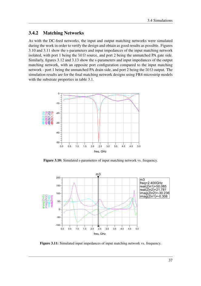
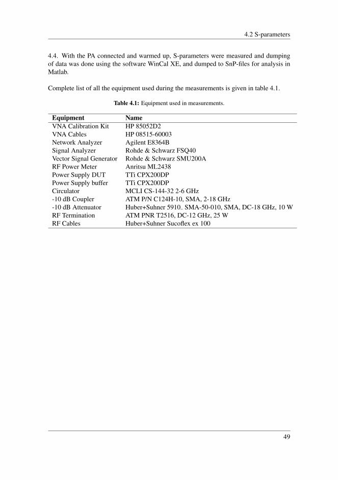
3.4.2 Matching NetworksAs with the DC-feed networks, the input and output matching networks were simulatedduring the work in order to verify the design and obtain as good results as possible. Figures3.10 and 3.11 show the s-parameters and input impedances of the input matching networkisolated, with port 1 being the 50 Ω source, and port 2 being the unmatched PA gate side.Similarly, figures 3.12 and 3.13 show the s-parameters and input impedances of the outputmatching network, with an opposite port configuration compared to the input matchingnetwork - port 1 being the unmatched PA drain side, and port 2 being the 50 Ω output. Thesimulation results are for the final matching network designs using FR4 microstrip modelswith the substrate properties in table 3.1.
Figure 3.10: Simulated s-parameters of input matching network vs. frequency.
! "! # !
Figure 3.11: Simulated input impedances of input matching network vs. frequency.
37
Chapter 3. Design and Simulation of GaN PA
!!!!!
!!!!!
Figure 3.12: Simulated s-parameters of output matching network vs. frequency.
!"
# #$#$ #$#$
$
Figure 3.13: Simulated input impedance of output matching network vs. frequency.
38
3.4 Simulations
3.4.3 Complete Design
Once the matching networks showed the correct impedances and S-parameters, the fullPA design was completed by adding the matching networks to the PA design, running as-parameter simulation to verify unconditional stability. When the µ-factors seen in figure3.14 was achieved, complete simulations were performed. Relatively high µ can be seen,having a low extreme µ = 1.043 at 3.0 GHz, but at most frequencies staying above 1.150.
0.8 1.6 2.4 3.2 4.0 4.8 5.6 6.4 7.20.0 8.0
0.986
1.071
1.157
1.243
1.329
1.414
0.900
1.500
freq, GHz
Km
u_lo
adm
u_so
urce
Figure 3.14: Simulated µ (source) and µ′ (load) vs. frequency.
The simulated s-parameters are shown figure 3.15, with port 1 being the input and port 2being the output. At 2.4 GHz, a |S11| = −19 dB and |S21| = 14.3 dB can be seen.
0 1 2 3 4 5−40
−20
0
20
f (GHz)
S-pa
ram
eter
s(d
B)
|S11||S12||S21||S22|
Figure 3.15: Simulated s-parameters of full PA design vs. frequency.
39
Chapter 3. Design and Simulation of GaN PA
Finally the end design was simulated using the same harmonic balance simulation test-bench that was used in the load and source pulling, with the microstrip matching networksreplacing the load and source pull benches. The resulting power gain, output power andηPAE is shown in figures 3.16, 3.17 and 3.18 respectively. For the complete design, a flatgain of GT = 14.8 dB and GT = 12.8 dB at 38 dBm output power, where the PA is start-ing to enter compression. In addition, peak values of Po = 40.9 dBm and ηPAE = 61.5 %were achieved in simulations.
!"#
$""
Figure 3.16: Simulated GT and gain compression vs. output power.
!"
#$
Figure 3.17: Simulated fundamental and third harmonic Po vs. input power.
40
3.4 Simulations
Figure 3.18: Simulated ηPAE vs. output power.
41
Chapter 3. Design and Simulation of GaN PA
3.5 Fabrication of PrototypeIn order to produce a prototype of the PA, gerber files for milling the microstrip had to begenerated. The design was collected in one single file, eliminating all sub-designs suchas the matching and DC-feed networks. Thereafter the lumped components were replacedwith microstrip step models, in case they had not already been included. All lumpedcomponents that were to be used were 0603 size, except from some of the decoupling ca-pacitors, which were 1208, therefore gap lengths of 1 mm were used. Thus the completemicrostrip was converted from schematic to layout design, which is the basis for the milleddesign.
The design was intended to fit on a lab standard 85x85 mm2 aluminium cooling plate. Assuch boundaries were drawn in the bound:drawing layer, to define the outer edges of thePCB and correspond with the cooling plate. In order to get thermal and electric conduc-tion, the transistor also needs contact with the cooling plate, and therefore the boundarylayer was used to define the hole in the microstrip PCB where the transistor would beplaced.
The main RF path was then aligned with the SMA contacts at the end of the cooling plate,and 50 Ω lines were added for the PA to reach the SMA contacts. Also the DC feeds werealigned one on each side of the RF path to avoid getting the fan stubs too close to eachother, and the corners and sections far away from the circuit design were filled using theconductor layer, to use as ground planes and hopefully make milling of the PCB take alittle less time. Ultimately holes were defined to overlap with the ones in the cooling plateto make attachment with screws possible.
The layout design was exported as gerber/drill files, which by appointment were handed tothe Elprolab at NTNU, performing the milling. Once milled, lumped components, simpleDC-cables, the transistor and SMA-contacts were soldered on, and the PCB was attachedto the cooling plate. As RF capacitors, Johanson S-series EIA 0603 ceramic capacitors[20] in addition to 1% 0603 SMC resistors from Distrelec. Decoupling was done usingthe capacitors in table 3.3 on both the gate and drain sides of the PA, in the same orderas listed in the table with the 10 pF Johanson being the closest to the fan stubs and the10µF Murata the closest to the DC cable. The 10 pF was made sure to be as close to theintersection between the DC-feed λ/4-line and the fan stubs, but for the drain side thiswas not possible due to the double fan design. It therefore had to be installed at a distancefrom the intersection.
In order to test the performance of the PA, measurements were performed at the NTNUmicrowave laboratory. S-parameters were measured by performing using a vector networkanalyzer (VNA) and the power related performance by doing a Pin-Pout sweep. Beforethis could be done, a visual confirmation of stable operation was performed. This wasdone by examining the output power spectrum with a Signal Analyzer, using the sameoutput coupler termination as shown in figure 4.1, but without a RF drive signal, with bothunterminated and 50 Ω terminated input connector. The PA was confirmed to have no spu-rious components, and was also left on for about 15 minutes to check if oscillations wouldoccur with increasing temperature. No oscillations were detected, thus unconditional sta-bility could be assumed and measurements commence.
4.1 Output Power SweepThe power performance of the PA examined by sweeping input power and measuring theoutput power, using the setup in figure 4.1. A Rohde & Schwarz SMU200A vector signalgenerator was used to generate a signal, whose power was swept and, the output power ofthe PA was measured by a Rohde & Schwarz FSQ40 Signal Analyzer.
The signal generator was not able to supply a signal with sufficient power to drive the PAfully into compression, as that would require a PA input power exceeding 30 dBm. There-fore a driver, or buffer PA was required, and a previous wideband linear prototype PAbased on the same Cree CGH40010 HEMT was used, and insufficient input power wouldnot be a problem. To avoid damaging the driver in case of any reflections from the DUTPA, a circulator was included. This is a triport device that for a certain frequency bandtransmits from one port to only one of the other two. A circulator is shown in figure 4.2,where incident waves on port 1 go to port 2, while incident waves on port 2 go to port 3.The circulator used had a forward loss of approximately −0.5 dB, which was included inthe characterization of the driver.
45
Chapter 4. Measurements
Figure 4.1: Power sweep measurement setup.
In addition some passive loss was included on the output of the DUT PA, as the signal
Figure 4.2: Circulator port configuration.
analyzer has a maximum input power of 30 dBm, which is quite a bit less than the outputpower the PA was designed for. This was done using a directional coupler, which splits thesignal between two ports. The signal analyzer was connected to a port having a 10 dB losscompared to the input, and was further attenuated using a 10 dB, 2 W attenuator, whichshould give more than 10 dB headroom for the limit on the signal analyzer. The third porton the coupler was terminated with a 25 W rated termination load, dissipating the rest ofthe signal.
Single-tone measurements were then performed, sweeping the input power from −10 to22 dBm VSG output power, at 2.30 GHz, 2.35 GHz, 2.4 GHz, 2.45 GHz and 2.50 GHz andmeasuring the output power and DC drawn by the PA. Similarly a two-tone measurementwas done, with input signal consisting of two frequencies with 5 MHz spacing equallyspaced around 2.40 GHz. Matlab was used for automatization of the measurements, com-municating with the instruments over GPIB. Scripts were generated for looping VSG out-put levels and signal frequencies, while reading measured power and drain current for eachlevel.
Thereafter, in order to estimate the performance in an envelope tracking setup, single-tonepower sweeps at 2.4 GHz were performed, while sweeping the supply voltage in stepsof 2 V. The same setup as for the regular single-tone and two-tone measurements wereused, shown in figure 4.1, but the Matlab scripts were slightly modified. Functionalityfor communicating with the TTi CPX200DP power supply that was used already addedwas included in the previous single-tone measurements, but not used for setting the supplyvoltage. This was added such that the supply voltage could be swept for every even valueof VD between 4 and 28 V. A similar single-tone power sweep was then performed for
46
4.1 Output Power Sweep
every supply voltage level, however only at 2.4 GHz.
Following the measurements of the PA, the output coupler loss and the driver had to becharacterized, and Matlab was used for sweeping these for the same VSG output power asfor the DUT PA. First the loss of the cable between the VSG and the driver was measuredas,
Lpass,in [dB] = PFSQ − PSMU (4.1)
where PFSQ is the power measured by the signal analyzer, and PSMU is the power ofthe signal generator both in dBm. The coupler loss on the output of the PA could thus befound as
Lpass,out [dB] = PFSQ − PSMU − Lpass,in (4.2)
with the setup in figure 4.3 and the driver output power as
Pdriver [dBm] = PFSQ − Lpass,out (4.3)
which included the loss through the circulator. Pdriver could thus be used as the inputpower for the DUT PA, used for calculation of gain and PAE. Ideally input power wouldbe measured during the DUT PA measurements themselves, but the only RF power meterat the lab was already being used in other ongoing measurements. A quick measurementwas however possible, measuring the difference in actual power of the signal, and the val-ues indicated by the signal generator and signal analyzer.
(a) (b)
Figure 4.3: Setup for characterisation of output termination (a) and driver (b).
Having characterized the losses of the passive components and the gain of the driver PAthe measurement data of the DUT PA had to be corrected to achieve the correct outputpower and be able to calculate the gain and PAE of the PA. This was all done in Matlab, asthis was an easy and efficient option and the data had already been measured using Matlab.The calculated output power would be given as
Pout [dBm] = PFSQ − Lout (4.4)
47
Chapter 4. Measurements
where PFSQ is the power measured by the signal analyzer and Lout is the output passiveloss from (4.2). Having measured this, calculation of available gain and PAE of the PAwas possible. The available gain of the PA calculated as
GA [dB] = Pout − Pdriver (4.5)
where Pdriver is the output of the driver found in (4.3) and Pout the measured outputpower. The PAE of the PA would be given as
ηPAE [%] =10
Pout−3010 − 10
Pdriver−30
10
VDIdrain(4.6)
using the drain current Idrain in ampere and supply voltage VD in volts. Both Pout andPdriver were given in dBm, and had to be converted to W, the same as IdrainVD, in orderfor ηPAE to be calculated.
4.2 S-parametersIn addition to the power sweeps, an S-parameter characterization was performed using avector network analyzer (VNA), as shown in figure 4.4. No driver PA was used as thiswould make measurement of the input S-parameters, S11 and S21 impossible. Also, beinga small signal measurement, the extra gain was not needed. The same attenuation as in thelarge signal power sweeps was used even though the VNA power level of −20 dBm wasused, as the VNA has a maximum power rating of 30 dBm and damaging the VNA wouldbe regrettable.
Figure 4.4: S-parameter measurement setup.
SOLT calibration of the VNA was performed with the coupler-attenuator attached to port2, accounting for the loss introduced. The measured S-parameters would therefore be cor-rect at the entrance of the coupler, not the VNA cable, marked as ’reference plane’ in figure
48
4.2 S-parameters
4.4. With the PA connected and warmed up, S-parameters were measured and dumpingof data was done using the software WinCal XE, and dumped to SnP-files for analysis inMatlab.
Complete list of all the equipment used during the measurements is given in table 4.1.
Table 4.1: Equipment used in measurements.
Equipment NameVNA Calibration Kit HP 85052D2VNA Cables HP 08515-60003Network Analyzer Agilent E8364BSignal Analyzer Rohde & Schwarz FSQ40Vector Signal Generator Rohde & Schwarz SMU200ARF Power Meter Anritsu ML2438Power Supply DUT TTi CPX200DPPower Supply buffer TTi CPX200DPCirculator MCLI CS-144-32 2-6 GHz-10 dB Coupler ATM P/N C124H-10, SMA, 2-18 GHz-10 dB Attenuator Huber+Suhner 5910 SMA-50-010, SMA, DC-18 GHz, 10 WRF Termination ATM PNR T2516, DC-12 GHz, 25 WRF Cables Huber+Suhner Sucoflex ex 100
49
Chapter 4. Measurements
50
Chapter 5Results and Envelope Tracking
Having performed the measurements as described in chapter 4, comparison between theperformance of the PA and the specifications was possible. Table 5.1 shows the specifiedparameters, and their simulated and measured values. Center frequency is the frequencyat which the PA is optimized for operation, where the specifications for input reflection,output power and available gain applies. The 1 dB bandwidth is defined as the frequencyrange around the center frequency with less than 1 dB gain than at the center frequency.
Table 5.1: Comparison between specified parameters and their simulated and measured values.
Parameter Specification Simulated MeasuredCenter frequency, f0 2.4 GHz 2.390 GHz 2.395 GHz1 dB bandwidth, B1 dB < 100 MHz 145 MHz 150 MHzInput reflection, |S11| < −10 dB −29.2 dB −14.0 dBOutput power at compression, Po 1 > 40 dBm 40.9 dBm 41.7 dBmAvailable gain, GA > 12 dB 12.7 dB 12.2 dB
The simulated and measured values for Po 1 is the maximum achievable single-tone outputpower, at 3 dB compression, while the values for GA is the single-tone gain at the pointwhere compression is starting to appear, that is at Po 1 = 38.0 dBm. The values for |S11|are the values at 2.4 GHz.Parameters that were not specified to be in any range, but are necessary in order to describethe performance of the amplifier correctly, are included in section 5.1.
51
Chapter 5. Results and Envelope Tracking
5.1 Static SupplyThe small and large signal characteristics of the PA operating from a static 28 V rail isshown in table 5.2. Specifications are included in table 5.1. The center frequency is the
Table 5.2: Complete list of measured parameters under static operation.
Parameter Simulated MeasuredCenter frequency, f0 2.390 GHz 2.395 GHz1 dB bandwidth, B1 dB 145 MHz 150 MHzPeak single-tone output power, Po 1 40.9 dBm 41.7 dBmPeak two-tone output power, Po 2 40.0 dBm 39.2 dBmPeak single-tone drain efficiency, η1 71.6% 78.0%Peak single-tone PAE, ηPAE 1 61.5% 68.2%Peak two-tone PAE, ηPAE 2 47.0% 56.3%Single-tone 1 dB compression point, P1 dB, 1 40.0 dBm 41.0 dBmTwo-tone 1 dB compression point, P1 dB, 2 37.8 dBm 38.5 dBmThird-order intermodulation, IMD3 −11.0 dBc −18.9 dBcSingle-tone Available gain, GA,1−tone 12.8 dB 12.2 dBTwo-tone Available gain, GA,2−tone 11.5 dB 10.2 dBInput reflection, |S11| −29.2 dB −14.0 dBSmall signal gain, |S21| 14.3 dB 14.1 dB
frequency at which the PA is designed for operation, and all parameters in table 5.2 aresupplied for this frequency, with exception of the two-tone parameters, where a signal con-sisting of two-tones at 2.395 GHz and 2.405 GHz was applied. B1 dB is still the frequencyrange with less than 1 dB gain compared to the center frequency.
The peak output power levels, Po 1 and Po 2 are both the peak output power, measured atPi 1 = 33.1 dBm and Pi 2 = 29.0 dBm respectively. For the two-tone signal this valuecorresponds to the tone power, which with two-tones of equal power yields a peak envelopepower 3 dB higher. Figure 5.1 shows the single-tone output power for corresponding inputpower values at 2.30, 2.35, 2.4, 2.45 and 2.50 GHz respectively. This figure shows thatthe peak output power at f0 is Po 1 = 41.68 dBm, for Pi 1 = 33.07 dBm. The peakvalues at the other respective frequencies are also shown to be at approximately this inputpower, but with lower output power due to the reduced gain. The 1 dB compression point,P1 dB, 1, can be found, as illustrated in figure 2.9, to be P1 dB, 1 = 41.0 dBm output power,for Pi 1 = 30.50 dBm.The single-tone available gain of the amplifier is plotted in figure 5.2 at the frequencies of2.30, 2.35, 2.4, 2.45 and 2.50 GHz.At all the frequencies the same general characteristic can be considered, however at lowerlevels for the frequencies furthest away from f0, as can also be seen as lowered outputpower in figure 5.1. At f0 however the, GA = 12 dB for Po 1 = 38.5 dBm, and the 1dB compression can be confirmed to be at Po 1 = 41.0 dBm, where GA = 10.5 dB. Thepeak output power, Po 1 = 41.68 dBm is reached in deep compression, with GA = 8.5dB, dropping quickly.
52
5.1 Static Supply
18 20 22 24 26 28 30 32 34
28
30
32
34
36
38
40
42
Input Power (dBm)
Out
putP
ower
(dB
m)
2.30 GHz2.35 GHz2.40 GHz2.45 GHz2.50 GHz
Figure 5.1: Single-tone output power characteristics.
18 20 22 24 26 28 30 32 34 36 38 40 420
2
4
6
8
10
12
14
Output Power (dBm)
Ava
ilabl
eG
ain
(dB
)
2.30 GHz2.35 GHz2.40 GHz2.45 GHz2.50 GHz
Figure 5.2: Single tone available gain as function of output power.
The ηPAE of single tone signals at 2.30, 2.35, 2.4, 2.45 and 2.50 GHz is shown in figure5.3. The individual curves are not easy to distinguish from one another as there is not as
53
Chapter 5. Results and Envelope Tracking
large difference in ηPAE for the respective frequencies at power levels other than the onesclose to peak. For f0 however a ηPAE = 68.4 % can be seen for Po 1 = 41.66, essentiallyat the peak output power.
18 20 22 24 26 28 30 32 34 36 38 40 420
10
20
30
40
50
60
70
Output Power (dBm)
PAE
(%)
2.30 GHz2.35 GHz2.40 GHz2.45 GHz2.50 GHz
Figure 5.3: single-tone a ηPAE as function of output power.
54
5.1 Static Supply
Figure 5.4 shows the results from the two-tone power sweep, which was only done around2.4 GHz. Peak two-tone output power can be found to be Po 2 = 39.2 dBm, for a Pi 2 =29.0 dBm, however at this point the PA is not fully compressed. The fundamental outputpower is included for comparison.
18 20 22 24 26 28 30 32 3430
35
40
Input Power (dBm)
Out
putP
ower
(dB
m)
Two-toneSingle-tone
Figure 5.4: Measured two-tone output power vs. input power.
Figure 5.5 shows the gain computed from the output power in figure 5.4. A slight reductiongain relative to the single-tone gain is apparent, crossing the GA = 12 dB line at Po 2 =36.1 dBm, and having a GA = 10.2 dB at the peak output power, Po 2 = 39.2 dBm.
20 25 30 35 400
5
10
15
Output Power (dBm)
Ava
ilabl
eG
ain
(dB
)
Two-toneSingle-tone
Figure 5.5: Measured two-tone available gain vs. Po 2
The two-tone ηPAE 2 of the PA is presented in figure 5.6 along with the single-toneηPAE 1. As the output power does not go as high, the peak power-added efficiency isonly ηPAE 2 = 56.3 % at Po 2 = 39.2 dBm. For lower power values however, the singleand two-tone curves follow one another closely, with the two-tone power added efficiencyeven slightly higher in the range between Po 2 = 32 dBm and Po 2 = 38 dBm.
55
Chapter 5. Results and Envelope Tracking
20 25 30 35 400
20
40
60
Output Power (dBm)
PAE
(%)
Two-toneSingle-tone
Figure 5.6: Measured two-tone ηPAE vs. Po 2
The 3rd order intermodulation distortion measured in the two-tone test is shown in figure5.7 in dB relative to the carrier, dBc. Below Po 2 = 35 dBm the intermodulation is below-30 dBc, and rapidly growing to a peak value of IMD3 = −18.9 at the peak output power,Po 2 = 39.2 dBm.
20 25 30 35 40−60
−40
−20
Output Power (dBm)
3rd
orde
rIM
D(d
Bc)
Lower endHigher end
Figure 5.7: Measured 3rd order IMD vs. Po 2
The measured s-parameters are shown in the following figures. S11 and S22 are displayedin 5.8 while S21 and S12 are displayed in rectangular plots in figures 5.9 and 5.9, respec-tively. S-parameters were measured two times, as a faulty measurement of S22 was discov-ered and recalibration had to be done. Difference in absolute value of the s-parameters areshown in figures B.8 and B.9, showing corresponding responses for the other s-parameters.
Considering the input reflection, S11, and output reflection, S22, in figure 5.8, plotting isdone for f ∈ (1.90 GHz , 2.90 GHz ) to be able to see the values in a 1 GHz band aroundf0. A mismatch can be seen, as neither S11 nor S22 cross through the center of the smith
56
5.1 Static Supply
diagram, but approximately 50 Ω with some capacitive reactance, at f0 . The mismatchleads to input and output return loses |S11| = −13.4 dB and |S22| = −13.8 dB at f0 asseen in figure B.9.
As for the forward gain, |S21|, the measurements show |S21| = 14.1 dB, at 2.40 GHz.However reviewing the data closer it is apparent that the matched frequency is 2.395 GHz,where |S21| = 14.15 dB. In addition the 1 dB bandwidth around f0 to be B1 dB =(2.31 GHz , 2.46 GHz ), or 150 MHz. |S12| is displayed in figure 5.10, showing fair iso-lation across the whole range, with a maximum of |S12| = −31.5 dB at 2.4 GHz.
Although the PA was considered unconditionally stable from evaluating the output spec-trum, µ was calculated from the s-parameters using (2.30), and is shown in figure B.7.
0.1
0.2
0.3
0.4
0.5
0.6
0.7
0.8
0.9
1.0
1.2
1.4
1.6
1.8
2.0
3.0
4.0
5.0
10 20
20
-20
10
-10
5.0
-5.0
4.0
-4.0
3.0
-3.0
2.0-2.
0
1.8-1
.8
1.6
-1.6
1.4
-1.4
1.2
-1.2
1.0
-1.0
0.9
-0.9
0.8
-0.8
0.7
-0.7
0.6-0
.6
0.5-0.
5
0.4
-0.4
0.3
-0.3
0.2
-0.2
0.1
-0.1
freq (1.918GHz to 2.907GHz)
S(1
,1)
S(2
,2)
Figure 5.8: Measured S11 and S22 in smith chart.
57
Chapter 5. Results and Envelope Tracking
0 1 2 3 4 5 6 7 8 9 10−20
−10
0
10
20
Frequency (GHz)
S-pa
ram
eter
s(d
B)
|S21|
Figure 5.9: Measured |S21| for complete design.
0 1 2 3 4 5 6 7 8 9 10−60
−50
−40
−30
Frequency (GHz)
|S12|(
dB)
|S12|
Figure 5.10: Measured |S12| for complete design.
58
5.2 Envelope Tracking Trajectories
5.2 Envelope Tracking TrajectoriesThe large signal characteristics of the PA were also investigated at reduced supply volt-ages in order to estimate the performance in an envelope tracking setup. The result beinga similar collection of curves as seen in figure 2.19. As the resulting trajectories can givevarying performance and complexity, a series of cases of desired characteristics are to beinvestigated. These are tracking for maximum efficiency, tracking for flat gain and linearcontrolling of the supply, and will be investigated in the following sections.
5.2.1 Maximum EfficiencyThe first case to be analyzed is tracking the amplifier to stay in compression also at re-duced input levels by reducing the supply voltage. Figure 5.11 presents the single-toneηPAE between 28 and 14 V in steps of 2 V descending from right to left. In additionthe resulting trajectory from successfully tracking for maximum efficiency is seen on thepeaks of the curves, which results in an improved ηPAE = 52 % at Po 1 = 35 dBm, as op-posed to ηPAE = 35 % during static 28 V operation. For power levels below Po 1 = 35.3dBm, the supply voltage is kept at VD
2 = 14V , as not much more improvement is achievedcompared to the reduction in gain.
20 22 24 26 28 30 32 34 36 38 40 420
10
20
30
40
50
60
70
Output Power, (dBm)
PAE
(%)
14 V16 V18 V20 V22 V24 V26 V28 VTrackSquare
Figure 5.11: ηPAE-curves and maximum efficiency trajectory vs. Po 1.
By following this trajectory a gain characteristic as seen in figure 5.12 is achieved. As aresult of tracking in quite deep compression, the resulting gain is not very high, rangingfrom 9 dB at peak output power to 6.6 dB for Po 1 = 35.4 in a highly nonlinear fashion,
59
Chapter 5. Results and Envelope Tracking
before following the 14 V curve.
20 22 24 26 28 30 32 34 36 38 40 420
2
4
6
8
10
12
14
Output Power, (dBm)
Ava
ilabl
eG
ain
(dB
)
14 V16 V18 V20 V22 V24 V26 V28 VTrackSquare
Figure 5.12: GA-curves and maximum efficiency trajectory vs. Po 1.
Similarly the resulting output power trajectory is shown in figure 5.13. The shape of this isclose to the shape of the gain curve, highly nonlinear, and drops rapidly into compressionat the 28 V curve.
The resulting supply voltage functions can be computed using (2.58), and drain voltage isshown vs. output and input voltage in figure 5.14.The drain supply voltage is a fairly linear response relative to the output RF voltage. This
is due to the high efficiency of operation, where as much of the supplied voltage is trans-mitted on the output, and therefore it lies close to the forbidden zone where Vout > VS .When plotted versus the input RF voltage however a highly nonlinear supply response canbe seen, due to the nonlinear gain. This is worth noting as this is the voltage gain a supplymodulator need in order to track for maximum efficiency.
Included in figure 5.14 is also a curve called square, which is a quadratic interpolationbetween Vout = 0 V and Vout = 28 V, as a possible alternative supply response. Theresulting ηPAE , output power and gain curves are shown in blue in figures 5.11, 5.13 andfigure 5.12 respectively. This is an attempt at trading off some ηPAE performance in favorof a nicer supply characteristic.
60
5.2 Envelope Tracking Trajectories
18 20 22 24 26 28 30 32 3415
20
25
30
35
40
Pin
P out
14 V16 V18 V20 V22 V24 V26 V28 VTrackSquare
Figure 5.13: Po 1-curves and maximum efficiency trajectory vs. Pi 1.
0 10 20 300
10
20
30
Vout
Vdr
ain
TrackForbiddenSquare
(a)
0 2 4 6 80
10
20
30
Vin
Vdr
ain
TrackSquare
(b)
Figure 5.14: Drain voltage vs. PA output (a) and input (b) voltage for maximum efficiency tracking.
61
Chapter 5. Results and Envelope Tracking
5.2.2 Flat Gain
A different way of tracking the PA can be choosing a trajectory that ensures a flat gaincharacteristic. The results while doing this will be presented for a flat available gain of 12dB, 10 dB and 9 dB.
12 dB
By tracking for 12 dB flat gain, the goal a gain characteristic as seen in figure 5.15. Herethe measured gain curves of the PA is shown between 28 and 14 V in steps of 2 V de-scending from right to left, with the ideal track crossing each curve where it yields 12 dBgain. For an instantaneous output power greater than Po 1 = 38.2 dBm the supply voltageis held at 28 V constant as any lower values give less gain, if the given output power isobtainable at all.
20 22 24 26 28 30 32 34 36 38 40 420
2
4
6
8
10
12
14
Output Power, (dBm)
Ava
ilabl
eG
ain
(dB
)
14 V16 V18 V20 V22 V24 V26 V28 VTrackSquare
Figure 5.15: GA-curves and 12 dB flat gain tracking trajectory vs. Po 1.
When looking at the output power, the resulting characteristic can be viewed in figure 5.16,which naturally is very similar to the gain characteristic.The resulting ηPAE is shown in figure 5.17, showing ηPAE = 38% for Po 1 = 35 dBm,
which is not an as large improvement over the 28 V curve at ηPAE = 35%, as whentracking for maximum efficiency.
The drain supply voltage vs. output and input signal voltage in figure 5.18. These re-sponses show quite similar behavior, quite linear tracking from about Vdrain = 20 V to
62
5.2 Envelope Tracking Trajectories
18 20 22 24 26 28 30 32 3415
20
25
30
35
40
Pin
P out
14 V16 V18 V20 V22 V24 V26 V28 VTrackSquare
Figure 5.16: Po 1-curves and 12 dB flat gain tracking trajectory vs. Pi 1.
20 22 24 26 28 30 32 34 36 38 40 420
10
20
30
40
50
60
70
Output Power, (dBm)
PAE
(%)
14 V16 V18 V20 V22 V24 V26 V28 VTrackSquare
Figure 5.17: ηPAE-curves and 12 dB flat gain tracking trajectory vs. Po 1.
Vdrain = 28 V while Vout = 2 V, Vin = 0.25 V and Vout = 20 V, Vin = 4.5 V, respec-tively. For the peak levels operation is done with constant 28 V supply.
63
Chapter 5. Results and Envelope Tracking
0 10 20 300
10
20
30
Vout
Vdr
ain
TrackSquareForbidden
(a)
0 2 4 6 80
10
20
30
Vin
Vdr
ain
TrackSquare
(b)
Figure 5.18: Drain voltage vs. PA output (a) and input (b) voltage for 12 dB flat gain tracking.
As an alternative to the ideal track, shown in red, a square supply function is analyzed,showing the resulting ηPAE , power gain and output power in figures 5.17, 5.15 and 5.16respectively. By doing this the PA operates at a higher supply than would give the de-sired flat gain operation, especially at lower signal levels, thus increasing the gain closerto 13 dB at Po 1 = 29 dBm and lower. A slight reduction in ηPAE at lower signal levelsis also a consequence of this.
64
5.2 Envelope Tracking Trajectories
10 dB
As the PA is operating at 28 V for a rather large dynamic range when tracking for 12 dBflat gain, the efficiency could possibly be improved by operating closer to compression.By lowering the constraint to 10 dB flat gain, as seen in figure 5.19, the tracking trajectorywould pass through the individual gain curves closer to compression than for 12 dB flatgain.
20 22 24 26 28 30 32 34 36 38 40 420
2
4
6
8
10
12
14
Output Power, (dBm)
Ava
ilabl
eG
ain
(dB
)
14 V16 V18 V20 V22 V24 V26 V28 VSquareTrack
Figure 5.19: GA-curves and 10 dB flat gain tracking trajectory vs. Po 1.
In this case, the range where following the 28 V cirve is reduced, starting the trackingat Po 1 = 41.3 dBm, as can be seen in figure 5.19 and 5.20. The power response infigure 5.20 shows the effect of the reduced gain constraint, staying in compression fromPi 1 = 26 dBm and all the way to peak power.
The efficiency resulting from this extended dynamic range at which the PA stays in com-pression is shown in figure 5.21. At Po 1 = 35 dBm, ηPAE = 47%, a 9% improvementgained from the 2 dB gain trade off.
Obtaining a 10 dB flat gain tracking characteristic is done using the supply response infigure 5.22. The supply response is a fair bit lower, and closer to the forbidden zonecompared to the 12 dB as operation in deeper compression is wanted. However as a resultthe response is somewhat curved, and resembles the square, alternative, response fairlyclosely.
65
Chapter 5. Results and Envelope Tracking
18 20 22 24 26 28 30 32 3415
20
25
30
35
40
Pin
P out
14 V16 V18 V20 V22 V24 V26 V28 VSquareTrack
Figure 5.20: Po 1-curves and 10 dB flat gain tracking trajectory vs. Pi 1.
20 22 24 26 28 30 32 34 36 38 40 420
10
20
30
40
50
60
70
Output Power, (dBm)
PAE
(%)
14 V16 V18 V20 V22 V24 V26 V28 VSquareTrack
Figure 5.21: ηPAE-curves and 10 dB flat gain tracking trajectory vs. Po 1.
66
5.2 Envelope Tracking Trajectories
0 10 20 300
10
20
30
Vout
Vdr
ain
TrackSquareForbidden
(a)
0 2 4 6 80
10
20
30
Vin
Vdr
ain
TrackSquare
(b)
Figure 5.22: Drain voltage vs. PA output (a) and input (b) voltage for 10 dB flat gain tracking.
67
Chapter 5. Results and Envelope Tracking
9 dB
Wanting to characterize the PA for several cases, the possibility of a scenario hopefullyjoining together the best features of both the maximum efficiency and flat gain would beinvestigated as 9 dB flat gain. This gain trajectory is shown in figure 5.23, where track-ing is done almost all the way to peak power, reaching the 28 V curve at Po 1 = 41.5 dBm.
20 22 24 26 28 30 32 34 36 38 40 420
2
4
6
8
10
12
14
Output Power, (dBm)
Ava
ilabl
eG
ain
(dB
)
14 V16 V18 V20 V22 V24 V26 V28 VSquareTrack
Figure 5.23: GA-curves and 9 dB flat gain tracking trajectory vs. Po 1.
The 9 dB flat gain trajectory fields an even larger dynamic range in which the PA is com-pressed, starting even slightly at Pi 1 = 23 dBm, as seen in figure 5.24. With 9 dBm gain,this equates to Po 1 = 32 dBm, yielding a 8 dBm dynamic range where tracking leads tothe PA operating in compression.
The ηPAE for the case with 9 dB flat gain is shown in figure 5.25. The resulting trajectorycan be seen to intersect the individual ηPAE-curves very close to the peaks, however thisis only the case for the 28 V and 26 V curves, at Po 1 = 41.1 dBm and Po 1 = 41.6 dBm,respectively. At larger back off than this, the curves are intersected further away fromtheir peak values, at lower ηPAE . The linear interpolation between the individual pointshowever show that the trajectory will be close to maximum anyway. An example of thiscan be seen at Po 1 = 36.7 dBm, where the ηPAE with VD = 18 V approximately equalsthe ηPAE with VD = 16 V. At Po 1 = 35.0 dBm, the ηPAE = 48 %, yielding a 13 %increase compared to fixed 28 V operation.
The drain supply response needed for this behavior is shown in figure 5.26. As with the10 dB flat gain case, a curved response is needed, with the 10 dB one perhaps a slightbetter fit to the square alternative. The close resemblance of the square alternative track-
68
5.2 Envelope Tracking Trajectories
18 20 22 24 26 28 30 32 3415
20
25
30
35
40
Pin
P out
14 V16 V18 V20 V22 V24 V26 V28 VTrackSquare
Figure 5.24: Po 1-curves and 9 dB flat gain tracking trajectory vs. Pi 1.
20 22 24 26 28 30 32 34 36 38 40 420
10
20
30
40
50
60
70
Output Power, (dBm)
PAE
(%)
14 V16 V18 V20 V22 V24 V26 V28 VSquareTrack
Figure 5.25: ηPAE-curves and 9 dB flat gain tracking trajectory vs. Po 1.
ing function however leads its gain, output power, ηPAE , plotted in blue in figures 5.23,5.24 and 5.25 respectively, being equal to the ideal track, seen in red. This is due to theresolution of the data being too low, only having measurements for every 20 V, and the
69
Chapter 5. Results and Envelope Tracking
deviation between the square and ideal tracking function is less than 1 V. The resultingperformance for the square track would therefore be slightly worse than the ideal.
0 10 20 300
10
20
30
Vout
Vdr
ain
TrackSquareForbidden
(a)
0 2 4 6 80
10
20
30
Vin
Vdr
ain
TrackSquare
(b)
Figure 5.26: Drain voltage vs. PA output (a) and input (b) voltage for 9 dB flat gain tracking.
70
5.2 Envelope Tracking Trajectories
5.2.3 Linear VD vs. Vin
In addition to tracking for maximum efficiency and flat gain, a case where the supplyvoltage is a linear function of the input signal voltage, as shown in figure 5.27(b), in orderto estimate the performance of the PA in such a case. This was done by starting the trackingat two different power gains, 12 dB and 10 dB respectively. The supply was then reducedlinearily with the output signal voltage, and mapped to create trajectories for the respectivebasis.
0 10 20 300
10
20
30
Vout
Vdr
ain
12 dB10 dBForbidden
(a)
0 2 4 6 80
10
20
30
Vin
Vdr
ain
12 dB10 dB
(b)
Figure 5.27: Drain voltage vs. PA output (a) and input (b) voltage for linear VD tracking.
A 4 V lower bound was chosen to ensure a nonzero supply at all times, resulting in the de-picted response. The supply plotted vs. the output power, in figure 5.27(b), is the resultingsupply response, and was not used as a basis for defining the trajectory.
The power gain resulting from the linear tracking is shown in figure 5.28, and can beseen to have a nonlinear response. This is due to the response being linear all the wayto Vin = 0 V, not clipped at e.g. Vout = 14 V as in figure 5.14. The gain curves foreven lower supply levels are therefore also included. The gain drops rather fast and atPo 1 = 35.0 dBm the gain is 10.75 dB and 8.5 dB for the 12 dB and 10 dB curves respec-tively.
The output power can be seen in figure 5.29. As an effect of the reduced gain, a reducedpower response is evident, needing Pi 1 = 23.8 dBm and Pi 1 = 25.8 dBm to get toPo 1 = 35.0 dBm, along the 12 dB and 10 dB trajectories respectively.
The resulting ηPAE is shown in figure 5.30, quite different efficiencies for the 12 dB and10 dB solutions. 10 dB gain is sufficiently deep compression that tracking is performedalmost all the way to peak output power, and as the trajectory taken keeps the PA com-pressed at lower supply levels, the ηPAE-trajectory is close to maximum possible. The12 dB gain alternative keeps constant 28 V supply for Po 1 = 38.0 dBm and greater, and
Figure 5.29: Po 1-curves and linear VD tracking trajectory vs. Pi 1.
tracks through each individual curve at fairly large back off, however closing in on the10 dB gain trajectory at Po 1 = 30.0 dBm and lower. At Po 1 = 35.0 dBm there is im-provement over static 28 V operation however, at ηPAE = 51 % and ηPAE = 43 % forthe 10 dB and 12 dB trajectories respectively.
Figure 5.30: ηPAE-curves and linear VD tracking trajectory vs. Po 1.
73
Chapter 5. Results and Envelope Tracking
74
Chapter 6Discussion
6.1 Static Supply Performance
Reviewing the measurement results in table 5.1, performance can be considered to fulfillthe specifications. However the grade at which specifications are met, is dependent on themeaning of the specifications. That is, at what output power should GA > 12 dB, should|S11| < −10 dB across the whole B1 dB-band, and is Po 1 > 40 dBm the peak outputpower, or where an output power that should be reached without entering compression. Inany case, the performance is not too far away from specified values.
If considering the measured center frequency and 1 dB bandwidth however, f0 = 2.395 GHzis a deviation of 5 MHz. As this also turns out to be the simulated center frequency it islikely to not be a fabrication error or measurement error, but due to a poor design effort.No matter the reason it can be considered a small problem, if a problem at all, as the re-sulting 1 dB bandwidth overlaps with the frequency range that would have been the 1 dBbandwidth with f0 = 2.4 GHz, B ∈ (2.35, 2.45) GHz, as shown in figure 6.1.
The input reflection, |S11| = −14.0 dB is the local minimum at 2.41 GHz, which is ac-
2.2 2.3 2.4 2.510
12
14
f (GHz)
|S21
(dB
)| Measured |S21|Simulated |S21|Measured B1 dB
Figure 6.1: Comparison between simulated and measured |S21|, and 1 dB bandwidths.
75
Chapter 6. Discussion
cording to specifications, considering that it is not meant as |S11| < −10 dB ∀ f ∈ B1 dB.The measurements show that this is only the case for f ∈ (2.37 GHz, 2.447 GHz). In anycase |S11| = −14.0 dB is not very impressive, as it results an input return loss, wastingpower and improving the risk of the reflection damaging whatever preceeds the PA in thetransmission chain. The latter can however be solved by a circulator, coupler or similar.Comparing to the simulated values, as seen in figure B.10 a better match would have beenexpected.
What is a problem actually is the large |S21| at frequencies lower than B1 dB. There aresmall dips of |S21| = 9.4 dB at 1.95 GHz and |S21| = 8.5 dB at 1.3 GHz, but apart fromthose |S21| > 10 dB for frequencies above 100 MHz even as high as 21 dB. This is ofcourse not good as it raises the chance of out-of-band transmission and instability, andshould have been suppressed. This should have been paid more attention to when design-ing the IMN and OMN, as |S21| in the frequency range is rather large, causing the overall|S21| to approach the MAG. The overall consequence is requiring to high-pass filter thesignal prior to, but possibly also following, the PA, which is unnecessary as this shouldhave been done using the matching networks. And in the case of needing a wideband PA,there are most likely better options, having a smoother gain characteristic.
According to figure B.8, the measured s-parameters show a fairly questionable S22, whicheven exceeds 0 at some frequencies. As this is strange, a control measurement was per-formed, having recalibrated the VNA, suspecting the distortion being result of bad cali-bration. As can be seen in figure B.9, a smoother response is achieved after recalibration,with similar values for the other s-parameters.
Fairly convincing however is the output power, which when the PA operates in deep com-pression reaches 41.7 dBm. As a result, the specified output power, 40.0 dBm, can bereached without compressing too much, increasing the gain at Po 1 = 40.0 dBm com-pared to Po 1 = 41.7 dBm. Compared to if the peak power was reduced, and the gaincurve shifted downwards in power so that the peak aligns at aronud 40.0 dBm, less in-put power is needed, which means a less powerful driver can be used, and less power iswasted. A result is also reduced distortion, as this is worst in deep compression, but this isalso where the PA is the most efficient.
When operating without a output power constraint a peak ηPAE = 68 % can be reachedat peak Po 1 = 41.7 dBm. However due to the higher output power the efficiency is re-duced if operating with 40.0 dBm maximum output power, yielding a peak ηPAE = 60 %,an 8 % reduction and 12 % deterioration. No specified value for ηPAE was supplied, butηPAE = 68 % is a 28 % improvement over [19], increasing the peak ηPAE by 15 %.
Also whether the power gain is according to specifications, depends on how they are inter-preted. A power gain exceeding 12 dB is experienced below about Po 1 = 38 dBm, whichcan be considered as the linear region gain. However due to the reduced conduction angleof class AB amplifiers, the gain is not constant beyond about Po 1 = 26 dBm, but linearilyreduced from 14.7 dB to 12 dB before compression kicks in. This is an intended reduction
76
6.1 Static Supply Performance
compared to [19], as it was desired to trade some of the excessive gain for efficiency.
Considering the measurement results that were not given any specified values, listed intable 5.2, the resulting linearity can be evaluated through the 1 dB compression point,P1 dB, 1. Thus the deviation from the linear gain trend, exceeds 1 dB beyond P1 dB, 1 =41.0 dBm, which allows for linear operation beyond a hypothetical power constraint at thespecified P1 dB, 1 = 40.0 dBm. Related is also the third order intermodulation distortion,IMD3, which at −18.9 dBc is a 1.1 dB increase compared to [19]. This was howevermeasured in the two-tone test, where the input power was not sufficient to drive the PAfully into compression, and would therefore likely be slightly higher. Comparing to thesimulated value, an estimated guess would be around −15 dBc. This is also used to esti-mate the saturated ACPR, which at −15 dBc peak is not very good, even being optimizedfor efficiency. At backoff, below Po = 35 dBm, however the IMD3 is below −30 dBc,which is just short of the performance presented in [21] and [22].
It is unfortunate the input power during the two-tone tests was capped, resulting in failureto characterize the PA performance in compression with a two-tone drive signal. The rea-son for this being the signal generator [23] having a maximum ouput peak envelope powerof 19 dBm, 7 dBm lower than the maximum single-tone power of 26 dBm. This couldhave been solved using a second driver PA, adding some gain to the signal chain and amp-ing the signal at the input of the DUT to a level that drives it into sufficient compression.However due to multiple time demanding ongoing projects, there was a limited amount ofequipment and time available for multiple measurements.
The measured peak two-tone parameters were however Po 2 = 39.2 dBm, GA,2−tone =10.2 dB and ηPAE 2 = 56, 3 %. Considering figures 5.4, 5.5 and 5.6 and simple extrapo-lating the curves, approaching Po 2 = 40 dBm, GA,2−tone = 8 dB and ηPAE 2 = 60 %could be approximated peak values.
It can also be questioned to what degree the design of the PA was good or not. Theperformance is satisfactory for some applications, but the PA is rather large. The outerboundaries were made to fit an 85× 85 mm2 cooling plate, and this was taking advantageof when designing the IMN and OMN, and the length of the design is barely fitting insidethe cooling plate. However the width of the design is far less than the width of the coolingplate, thus should the PA be commercialized it would likely be of interest to create a morecompact design. This could have been done if not trying to aviod using lumped compo-nents in the matching networks. Additionally the DC bias and supply cables could havebeen replaced with 4 mm connectors, or in case of ET, BNC connectors. In either case,the design serves its purpose as a prototype for investigating possibilities of ET well.
An overall, last-minute optimization of the PA was not performed as design was carriedout on a low-power ultrabook computer, having limited CPU power. This optimizationwas attempted, but aborted as optimization iterations took extremely long to complete andthe Elpro lab requested the finished design to be delivered shortly. Had this been com-pleted, even trying to limit the number of optimization variables and goals, or even using
77
Chapter 6. Discussion
a more powerful PC, the performance could have been improved slightly. Especially theinput return loss, although according to specifications, could have gained from this.
6.2 Envelope TrackingAs a means to characterize the ET performance of the PA, power sweeps at reduced sup-ply voltage levels were performed. As this is essentially a single-tone test, which meansthe supply voltage and RF signal amplitude can be considered constant in between beingchanged. Additionally a fixed supply uses solid decoupling on both drain and gate side,and when doing ET the drain side decoupling must be removed to avoid shorting the time-varying supply, which could introduce memory effects causing distortion. Also the timevarying supply will further Nonlinear simulations using the CGH40010 showing this isdone in [24]. Still, an envelope tracker is a low impedance termination, which will reducethe problem, but the performed measurements can still only be considered a fair estimateof the resulting ET performance.
Reviewing the results in section 5.2, a set of possible cases for tracking have been pre-sented, yielding different characteristics. Considering a 5-6 dB PAPR transmitted signal,which results in 35 dBm average output power, improvements to power-added efficiencyrange from 3 % to almost 20 %, and gain levels and responses vary greatly due to variablelevels of compression.
The ηPAE , available gain and supply voltage for the considered cases is compared infigures 6.2, 6.3 and 6.4, respectively.
Figure 6.2: Comparison of ηPAE vs. Po 1 for different tracking cases.
At 35 dBm output power the fixed 28 V ηPAE = 35 %, and the far smallest improvementsresulting from ET is the 12 dB flat gain, only giving an improvement for about three per-cent, that is ηPAE ≈ 38 %. The small improvement is a result of the tracked supply beingto high to keep the PA saturated, only being saturated at output power greater than aboutPo = 38 dBm, where the supply is fixed at 28 V.
78
6.2 Envelope Tracking
This is also the point at which the linear 12 dB tracking starts, but with a steeper supplyresponse, as seen in figure 6.4, resulting in staying closer to compression, and a largerimprovement to efficiency, yielding ηPAE = 44 %, a 6 % improvement over the 12 dBflat gain case. Except from the 10 dB flat gain case at about 47 %, the remaining cases allresult in roughly the same ηPAE at 35 dBm output power and beyond, and having betweenηPAE = 51 % and ηPAE = 52 %.
Figure 6.3: Comparison of GA vs. Po 1 for different tracking cases.
The improved ηPAE is a result of dynamic varying of the supply voltage, keeping the PAsaturated, or at least closer to saturation at back off. This however affects the gain of thePA, as can be seen in figure 6.3, where the most efficient cases yield the lowest and, withexception of the 9 db flat gain case, least linear gain. The gained energy efficiency maytherefore be lost as a larger input power is needed, which leads to a greater power dissi-pation for the system preceding the PA in the signal chain, and it may require more powerdemanding linearization, such as digital predistortion.
0 2 4 6 80
10
20
30
Vin
Vdr
ain
EfficiencyGain,12 dBGain, 10 dBGain, 9 dBLinear, 12 dBLinear, 10 dB
Figure 6.4: Comparison of VS vs. Vin for different tracking cases.
79
Chapter 6. Discussion
Another thing that may have a great impact on the overall system efficiency for the givencases is the envelope amplifier. This because the envelope bandwidth is several times theRF bandwidth, and either a complex, high-performance EA is needed, or using a low-performance EA, reducing the efficiency. Similarly if the envelope is not amplified cor-rectly the efficiency improvement of the RF PA is decreased.
Especially the maximum efficiency case is going to be hard to realize the supply responsefor, and the resulting gain response is fairly non-linear. The supply voltage tracking func-tion is however rather similar to the 9 dB flat gain case, but not compressing quite as much,raising the gain to about 9 dB. Conveniently enough it is also fairly similar to a square de-sign, thus reducing the bandwidth needed by the EA, possibly increasing its efficiency.This is also the case for the 10 dB flat gain case, but compressing a little less. The ef-ficiency is not too much worse, and it could as such be considered a fair alternative fortrading some efficiency for extra gain.
The 10 dB linear supply voltage case also gives a reasonable increase in efficiency of theRF PA, but also require high envelope bandwidths, especially if a lower level is set, asseen in figure 2.21. This is most likely required as well, as the gain is severely reduced atvoltages below 14 V, where it is reduced below 8 dB. The 12 dB flat gain and 12 dB lin-ear supply cases however may very well not improve ηPAE enough to improve the overallsystem efficiency, as the power dissipated by the EA may exceed the reduction in the RFPA.
The performance for the cases when applying a square supply function was also investi-gated. The overall improvement to efficiency was somewhat reduced due to the trackerkeeping the PA further away from compression, but especially for the 10 dB and 9 dBflat gain cases, the ideal supply function is already almost similar to the square function.Using a square supply function can thus be regarded as an alternative to the linear, as PAefficiency is not terrible in comparison, and as the tracker requirements are far lower for asquare function. In addition, as can be seen, the gain responses are far less linear for themaximum efficiency and linear supply cases, reducing the need for extensive predistortionin the flat gain cases. It could therefore be beneficial to investigate this deeper, bringingactual tracker characteristics into the calculation to estimate the overall system efficienciesfor the different cases.
80
Chapter 7Conclusion
In this thesis, the design of a 10 W class AB S-band power amplifier has been presented,displaying the potential of the GaN HEMT. Performance at static supply has been inves-tigated at center and possible bandlimit frequencies have been investigated, shown to bewithin specified limits. The load and source impedances of the PA has been optimized forefficiency by using load and source pull techniques, also achieving higher gain and widerbandwidth than specified. The PA featured a single-tone 41.7 dBm peak output powerwith 68.2% peak ηPAE and 12.2 dB uncompressed gain.
Despite meeting the specifications and fielding good overall performance, the s-parametermeasurements show a somewhat bad match, resulting in some input loss. Designing ofthe matching networks also failed to suppress low frequencies, resulting in high gain fromthe center frequency down to 100 MHz, which in some transmitters can be problematic.The possible solution of more extensive filtering in the rest of the system should not benecessary as this gain of the PA in question should have been suppressed.
In addition the PA was characterized at reduced supply voltages in order to estimate theperformance when employing envelope tracking. Three sets of cases were investigated,tracking for maximum efficiency, flat gain and linear supply response respectively. Themaximum efficiency case resulted in the largest possible improvement to the efficiency ofthe PA, but at the largest cost. The resulting gain was severely reduced and nonlinear. Incomparison, the flat gain cases had slightly less improvement to efficiency, but a nicer gainresponse. Applying a linear supply function yielded a fair improvement to the efficiency,but lowering gain at increasing back off. Based on the measurements conducted, improve-ments to ηPAE can be as high as 17 % at 5-6 dB back off when adding envelope tracking.
The measurements however show a clear trade off between gain and efficiency resultingin fairly poor gain for the cases with the largest improvement to efficiency. This can bedeceiving as reduced gain will increase the required input power, contributing to powerdissipation outside the PA and thus overall efficiency improvement may be reduced.
81
Chapter 7. Conclusion
The performance in the envelope tracking cases were also estimated when applying squaresupply functions. Deviating from their respective ideal tracking functions showed somereduction to the initial improvement, however the flat gain shows similar ideal supplyfunctions, minimizing the reduction. Utilizing a square function supply modulator canthus improve overall system efficiency, as less bandwidth is required by the supply mod-ulator, improving its respective efficiency. In any case a less complex supply can be used,reducing complexity and costs.
Further continuation on this project would include studying of the complete system for theinvestigated cases, including the efficiencies in order to determine which combination ofcase and envelope amplifier that result in the highest overall system efficiency.
In the case of further improving the PA, a rematch will be appropriate in order to reduce theinput return loss and deal with the low frequency gain. The source and load impedancesresulting from the source pull are thought to yield a good combination of efficiency andgain, however there could very well be better solutions. Should it be possible to increasethe gain at compression, the gain could be though to still be high even when tracking closeto compression and it Would be interesting to know the efficiency reduction.
82
Bibliography
[1] Zhanchang Wang. Envelope Tracking Power Amplifiers for Wireless Communica-tions. Artech House Inc., 1st edition, 2014.
[2] David M. Pozar. Microwave Engineering. Artech House Inc., 4th edition, 2011.
[3] Peter Cripps. RF Power Amplifiers For Wireless Communications. Artech HouseInc., 2nd edition, 2006.
[4] David M. Pozar. Microwave and RF Design of Wireless Systems. Artech House Inc.,1st edition, 2002.
[5] David K. Cheng. Field and Wave Electromagnetics. Addison Wesley PublishingCompany, Inc., 2nd edition, 1989.
[6] Michael Steer. Microwave and RF Design - A Systems Approach. Scitech PublishingInc., 1st edition, 2010.
[7] G. Gonzales. Microwave Transistor Amplifiers, Analysis and Design. Prentice-HallInc., 2nd edition, 1997.
[8] J. M. Rollett. Stability and power gain invariants of linear two-ports. IRE Trans.Circuit Theory, 9(1):29–32, 1962.
[9] M. L. Edwards and J. H. Sinsky. A new criteria for linear 2-port stability using asingle geometrically derived parameter. IEEE Trans. Microwave Theory and Tech-niques, 40:2803–2811, 1992.
[10] Peter B. Kenington. High-Linearity RF Amplifier Design. Artech House Inc., 1stedition, 2000.
[11] Frederick Raab, Peter Asbeck, Steve Cripps, Peter B. Kenington, Zoya B. Popovich,Nick Pothecary, John F. Sevich, and Nathan Sokal. RF and Microwave Power Am-plifier and Transmitter Technologies. IEEE Transactions on Microwave Theory andTechniques, 2002.
83
BIBLIOGRAPHY
[12] C. Weitzel. Will gaas survive for wireless pas?? In 2005 International Conferenceon Compound Semiconductor Manufacturing Technology.
[13] Pengellym Raymond S., Simon M. Wood, James W. Milligan, Scott T. Sheppard, andWilliam L. Pribble. Review of gan on sic high electron-mobility power transistorsand mmics. IEEE Transactions on Microwave Theory and Techniques, 60(6), June2012.
[14] Adel A. M. Saleh and Donald C. Cox. Improving the Power-Added Efficiency ofFET Amplifiers Operating with Varying-Envelope Signals. IEEE Transactions onMicrowave Theory and Techniques, 1983.
[15] E. McCune. Envelope Tracking or Polar - Which Is It? IEEE Microwave Magazine,June 2012.
[16] Rohde & Schwarz. The Crest Factor in DVB-T (OFDM) Transmitter Systems andits Influence on the Dimensioning of Power Components, 2007. Application Note.
[17] Sulaiman A. Aburakhia, Ehab F. Badran, and Darwish A. Mohamed. Distribution ofthe PAPR for Real-Valued OFDM Signals. International Conference on InformationTechnology (ICIT), 2009.
[18] Timo Aitto-oja. High efficiency envelope tracking supply voltage modulator for highpower base station amplifier applications. Microwave Symposium Digest (MTT),2010 IEEE MTT-S International, 2010.
[19] Bognøy, A. Design of a PA for use in an Envelope Tracking architecture. Technicalreport, NTNU, 2014.
[21] Junghwan Moon, Junghwan Son, Juyeon Lee, Jungjoon Kim, Seunghoon Jee, Se-ungchan Kim, and Bumman Kim. A multimode/multiband envelope tracking trans-mitter with broadband saturated power amplifier. IEEE MTT-S International Mi-crowave Symposium, 2011.
[22] P. Suebsombut, O. Koch, and S. Chalermwisutkul. Development of a GaN HEMTClass-AB Power Amplifier for an Envelope Tracking System at 2.45 GHz. Electri-cal Engineering/Electronics Computer Telecommunications and Information Tech-nology (ECTI-CON), 2010 International Conference on, 2010.
[23] Rohde & Schwarz. Vector Signal Generator SMU200A, September 2006.
[24] Junghwan Moon, Juyeon Lee, Junghwan Son, Jungjoon Kim, Seunghoon Jee, Se-ungchan Kim, and Bumman Kim. Effects of even-order terms on behavior model ofenvelope tracking transmitters. Microwave Integrated Circuits Conference (EuMIC),European, 2011.
84
Appendix AExtrapolation of Two-toneMeasurements
Due to the signal generator output power being insufficient to drive the PA into compres-sion during the two-tone measurement, simple extrapolation of the measurements weremade. Figures A.1, A.2 and A.3 show the measured two-tone output power, power gainand ηPAE and their corresponding extrapolations, respectively. The extrapolated thridorder intermodulation is shown in figure A.4.
26 28 30 32 3436
38
40
42
Input Power (dBm)
Out
putP
ower
(dB
m)
Two-toneSingle-toneExtrapolated
Figure A.1: Measured two-tone output power vs. input power.
85
Chapter A. Extrapolation of Two-tone Measurements
36 38 40 42
6
8
10
12
14
Output Power (dBm)
Tran
sduc
erPo
wer
Gai
n(d
B)
Two-toneSingle-toneExtrapolated
Figure A.2: Measured two-tone available gain vs. Po 2
36 38 40 4230
40
50
60
70
Output Power (dBm)
PAE
(%)
Two-toneSingle-toneExtrapolated
Figure A.3: Measured two-tone ηPAE vs. Po 2
30 32 34 36 38 40−35
−30
−25
−20
−15
Output Power (dBm)
3rd
orde
rIM
D(d
Bc)
Lower endHigher endExtrapolated
Figure A.4: Measured 3rd order IMD vs. Po 2
86
Appendix BFigures
ADS Design and Simulation
VarEqn
MTAPERMLIN MSTEP MLIN MTEE_ADS
MLEF
MTAPER JTCap0603
VAR
MLEF
MGAP
P1
MTEE_ADS
P2TermTerm Taper10
Gap3
TL16 TL13 Tee3
TL12
Taper6 Kap1
VAR2
TL11
Tee2
Num=1 Step2 Num=2Term2Term1 Subst="MSub1"
W1=1 mm -oW2=2.25 mmL=1 mm -o
S=1 mmW=0.625 mmSubst="MSub1"
ls=13.7323 t ols2=1.78396 t o
W2=wr mm
Subst="MSub1"W=wr mmL=lr mm L=ll mm
W=wl mmSubst="MSub1"
W3=ws2 mmW2=wl mmW1=wl mmSubst="MSub1"
L=ls2 mmW=ws2 mmSubst="MSub1"
L=1 mm -oW2=wl mmW1=1 mm -oSubst="MSub1" C=81.7146 t o
lr2=17.7938 t -olr=12.8775 t oll=8.28722 -t owl=4.94813 -t owt=4.96465 -owe=3.39291 t -owr=2.75288 t o
L=ls mmW=ws mmSubst="MSub1"
W3=ws mmW2=wr mmW1=3.04 mmSubst="MSub1" ws=1.53778 t o
ws2=1.63629 t o
W1=wl mmSubst="MSub1"
Z=18.05+j*31.845 OhmNum=2
Z=50 OhmNum=1
Figure B.1: Input matching network design in ADS
87
Chapter B. Figures
VarEqn
MSTEPMLIN
MTAPER
VAR
MLEF
JTCap0603MTEE_ADS MTAPER
MTEE_ADS
MLEF
MLIN TermTerm P2P1
Step2TL18
Taper6
VAR1
Tee2
Tee5
TL13
Kap2
TL11
Term2Term1 Num=2Num=1 Taper3TL10
W2=wl mmW1=wr mmSubst="MSub1"
L=ll mmW=wl mmSubst="MSub1"
Subst="MSub1"W1=wl mmW2=3.04 mmW3=ws mm
Subst="MSub1"
L=1 mm -ols2=5.37439 t ols=6.27916 -t o
wr=2.01083 t owl=2.00005 -t oll=4.78113 -t olr=13.4468 -t ows=3.99997 -t o