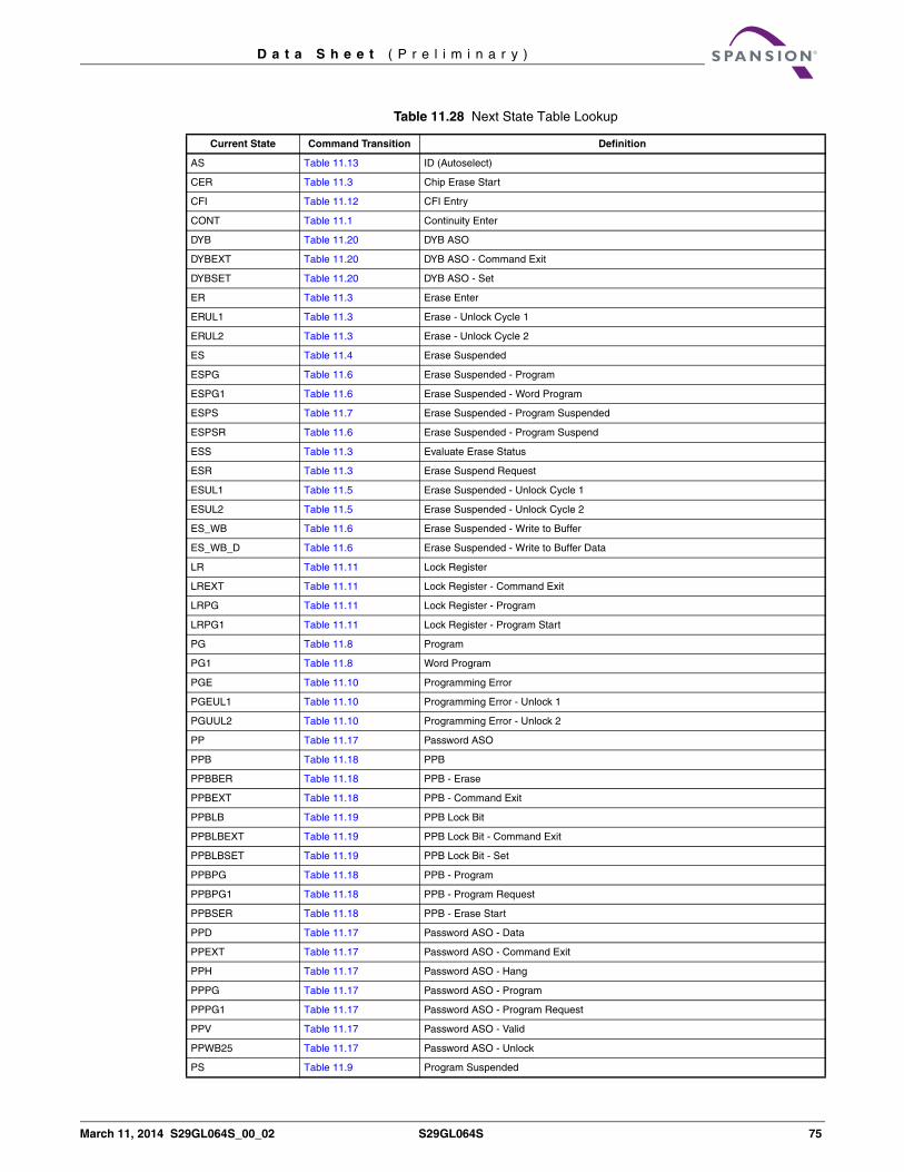
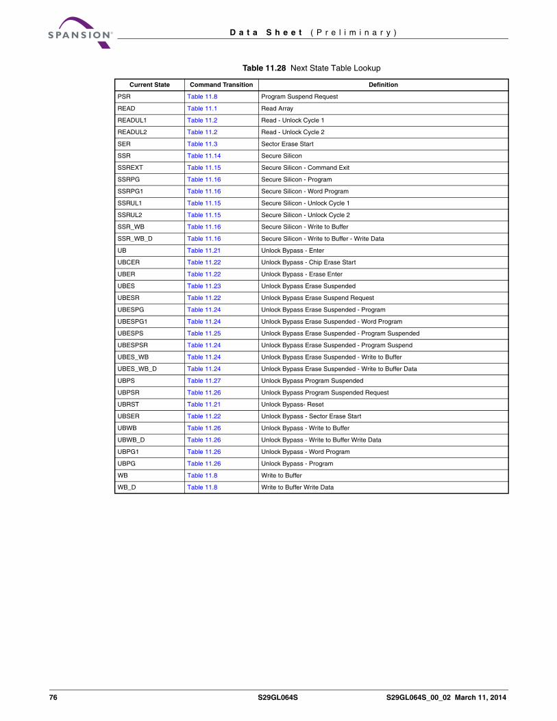
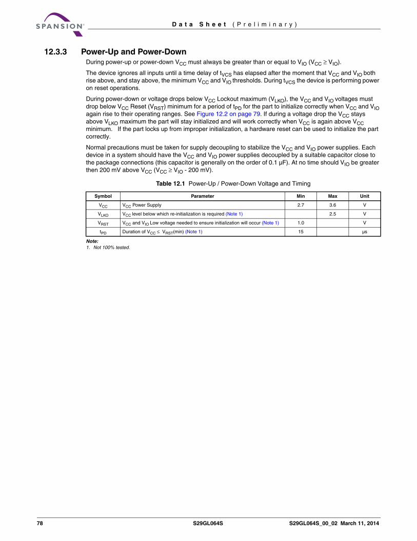
Publication Number S29GL064S_00 Revision 02 Issue Date March 11, 2014 S29GL064S MirrorBit ® Eclipse ™ Flash S29GL064S Cover Sheet S29GL064S 64 Mbit (8 Mbyte) CMOS 3.0 Volt Core with Versatile I/O Data Sheet (Preliminary) Notice to Readers: This document states the current technical specifications regarding the Spansion product(s) described herein. Each product described herein may be designated as Advance Information, Preliminary, or Full Production. See Notice On Data Sheet Designations for definitions.
Transcript
Publication Number S29GL064S_00 Revision 02 Issue Date March 11, 2014
S29GL064S MirrorBit® Eclipse™ Flash
S29GL064S Cover Sheet
S29GL064S 64 Mbit (8 Mbyte)CMOS 3.0 Volt Core with Versatile I/O
Data Sheet (Preliminary)
Notice to Readers: This document states the current technical specifications regarding the Spansion product(s) described herein. Each product described herein may be designated as Advance Information, Preliminary, or Full Production. See Notice On Data Sheet Designations for definitions.
2 S29GL064S S29GL064S_00_02 March 11, 2014
Notice On Data Sheet DesignationsSpansion Inc. issues data sheets with Advance Information or Preliminary designations to advise readers of product information or intended specifications throughout the product life cycle, including development, qualification, initial production, and full production. In all cases, however, readers are encouraged to verify that they have the latest information before finalizing their design. The following descriptions of Spansion data sheet designations are presented here to highlight their presence and definitions.
Advance InformationThe Advance Information designation indicates that Spansion Inc. is developing one or more specific products, but has not committed any design to production. Information presented in a document with this designation is likely to change, and in some cases, development on the product may discontinue. Spansion Inc. therefore places the following conditions upon Advance Information content:
“This document contains information on one or more products under development at Spansion Inc. The information is intended to help you evaluate this product. Do not design in this product without contacting the factory. Spansion Inc. reserves the right to change or discontinue work on this proposed product without notice.”
PreliminaryThe Preliminary designation indicates that the product development has progressed such that a commitment to production has taken place. This designation covers several aspects of the product life cycle, including product qualification, initial production, and the subsequent phases in the manufacturing process that occur before full production is achieved. Changes to the technical specifications presented in a Preliminary document should be expected while keeping these aspects of production under consideration. Spansion places the following conditions upon Preliminary content:
“This document states the current technical specifications regarding the Spansion product(s) described herein. The Preliminary status of this document indicates that product qualification has been completed, and that initial production has begun. Due to the phases of the manufacturing process that require maintaining efficiency and quality, this document may be revised by subsequent versions or modifications due to changes in technical specifications.”
CombinationSome data sheets contain a combination of products with different designations (Advance Information, Preliminary, or Full Production). This type of document distinguishes these products and their designations wherever necessary, typically on the first page, the ordering information page, and pages with the DC Characteristics table and the AC Erase and Program table (in the table notes). The disclaimer on the first page refers the reader to the notice on this page.
Full Production (No Designation on Document)When a product has been in production for a period of time such that no changes or only nominal changes are expected, the Preliminary designation is removed from the data sheet. Nominal changes may include those affecting the number of ordering part numbers available, such as the addition or deletion of a speed option, temperature range, package type, or VIO range. Changes may also include those needed to clarify a description or to correct a typographical error or incorrect specification. Spansion Inc. applies the following conditions to documents in this category:
“This document states the current technical specifications regarding the Spansion product(s) described herein. Spansion Inc. deems the products to have been in sufficient production volume such that subsequent versions of this document are not expected to change. However, typographical or specification corrections, or modifications to the valid combinations offered may occur.”
Questions regarding these document designations may be directed to your local sales office.
This document states the current technical specifications regarding the Spansion product(s) described herein. The Preliminary status of this document indicates that product qual-ification has been completed, and that initial production has begun. Due to the phases of the manufacturing process that require maintaining efficiency and quality, this documentmay be revised by subsequent versions or modifications due to changes in technical specifications.
Publication Number S29GL064S_00 Revision 02 Issue Date March 11, 2014
Distinctive Characteristics
Architectural Advantages Single Power Supply Operation
Manufactured on 65 nm MirrorBit Process Technology
Enhanced VersatileI/O Control– All input levels (address, control, and DQ input levels) and outputs
are determined by voltage on VIO input. VIO range is 1.65 to VCC
Compatibility with JEDEC Standards– Provides pinout and software compatibility for single-power supply
flash, and superior inadvertent write protection
100,000 Erase Cycles per Sector Minimum
20-year Data Retention Typical
Performance Characteristics High Performance
– 70 ns access time – 8-word / 16-byte page read buffer– 15 ns page read time – 128-word / 256-byte write buffer which reduces overall programming
time for multiple-word updates
Low Power Consumption– 25 mA typical initial read current @ 5 MHz– 7.5 mA typical page read current @ 33 MHz– 50 mA typical erase / program current– 40 µA typical standby mode current
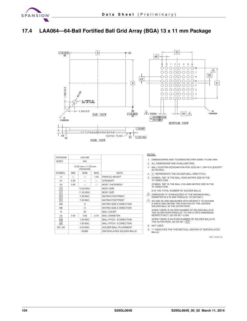
Package Options– 48-pin TSOP– 56-pin TSOP– 64-ball Fortified BGA (LAA064 13 mm x 11 mm x 1.4 mm)
(LAE064 9 mm x 9 mm x 1.4 mm)– 48-ball fine-pitch BGA (VBK048 8.15 mm x 6.15 mm x 1.0 mm)
Temperature Range– Industrial (-40°C to +85°C)– In-Cabin (-40°C to +105°C)
(when high voltage is applied). Protects first or last sector regardless of sector protection settings on uniform sector models
– Hardware reset input (RESET#) resets device– Ready/Busy# output (RY/BY#) detects program or erase cycle
completion
S29GL064S MirrorBit® Eclipse™ FlashS29GL064S 64 Mbit (8 Mbyte)CMOS 3.0 Volt Core with Versatile I/O
Data Sheet (Preliminary)
4 S29GL064S S29GL064S_00_02 March 11, 2014
D a t a S h e e t ( P r e l i m i n a r y )
General DescriptionThe S29GL-S mid density family of devices are 3.0-volt single-power flash memory manufactured using 65 nm MirrorBit technology. The S29GL064S is a 64-Mb device organized as 4,194,304 words or 8,388,608 bytes. Depending on the model number, the devices have 16-bit wide data bus only, or a 16-bit wide data bus that can also function as an 8-bit wide data bus by using the BYTE# input. The devices can be programmed either in the host system or in standard EPROM programmers.
Access times as fast as 70 ns are available. Note that each access time has a specific operating voltage range (VCC) as specified in the Product Selector Guide and Ordering Information – S29GL064S. Package offerings include 48-pin TSOP, 56-pin TSOP, 48-ball fine-pitch BGA, and 64-ball Fortified BGA, depending on model number. Each device has separate chip enable (CE#), write enable (WE#) and output enable (OE#) controls.
Each device requires only a single 3.0-volt power supply for both read and write functions. In addition to a VCC input, a high-voltage accelerated program (ACC) feature is supported through increased voltage on the WP#/ACC or ACC input. This feature is intended to facilitate system production.
The device is entirely command set compatible with the JEDEC single-power-supply flash standard. Commands are written to the device using standard microprocessor write timing. Write cycles also internally latch addresses and data needed for the programming and erase operations.
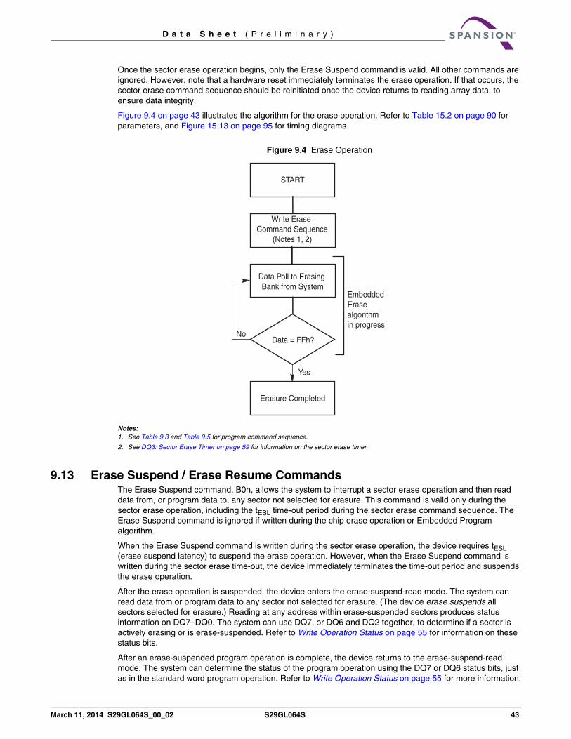
The sector erase architecture allows memory sectors to be erased and reprogrammed without affecting the data contents of other sectors. The device is fully erased when shipped from the factory.
The Advanced Sector Protection features several levels of sector protection, which can disable both the program and erase operations in certain sectors. Persistent Sector Protection is a method that replaces the previous 12-volt controlled protection method. Password Sector Protection is a highly sophisticated protection method that requires a password before changes to certain sectors are permitted.
Device programming and erasure are initiated through command sequences. Once a program or erase operation begins, the host system need only poll the DQ7 (Data# Polling) or DQ6 (toggle) status bits or monitor the Ready/Busy# (RY/BY#) output to determine whether the operation is complete. To facilitate programming, an Unlock Bypass mode reduces command sequence overhead by requiring only two write cycles to program data instead of four.
Hardware data protection measures include a low VCC detector that automatically inhibits write operations during power transitions. The hardware sector protection feature disables both program and erase operations in any combination of sectors of memory. This can be achieved in-system or via programming equipment.
The Erase Suspend / Erase Resume feature allows the host system to pause an erase operation in a given sector to read or program any other sector and then complete the erase operation. The Program Suspend / Program Resume feature enables the host system to pause a program operation in a given sector to read any other sector and then complete the program operation.
The hardware RESET# pin terminates any operation in progress and resets the device, after which it is then ready for a new operation. The RESET# pin may be tied to the system reset circuitry. A system reset would thus also reset the device, enabling the host system to read boot-up firmware from the flash memory device.
The device reduces power consumption in the standby mode when it detects specific voltage levels on CE# and RESET#, or when addresses are stable for a specified period of time.
The Write Protect (WP#) feature protects the first or last sector by asserting a logic low on the WP#/ACC pin or WP# pin, depending on model number. The protected sector is still protected even during accelerated programming.
The Secure Silicon Region provides a 128-word / 256-byte area for code or data that can be permanently protected. Once this sector is protected, no further changes within the sector can occur.
Spansion MirrorBit flash technology combines years of flash memory manufacturing experience to produce the highest levels of quality, reliability and cost effectiveness. The device electrically erases all bits within a sector simultaneously via hot-hole assisted erase. The data is programmed using hot electron injection.
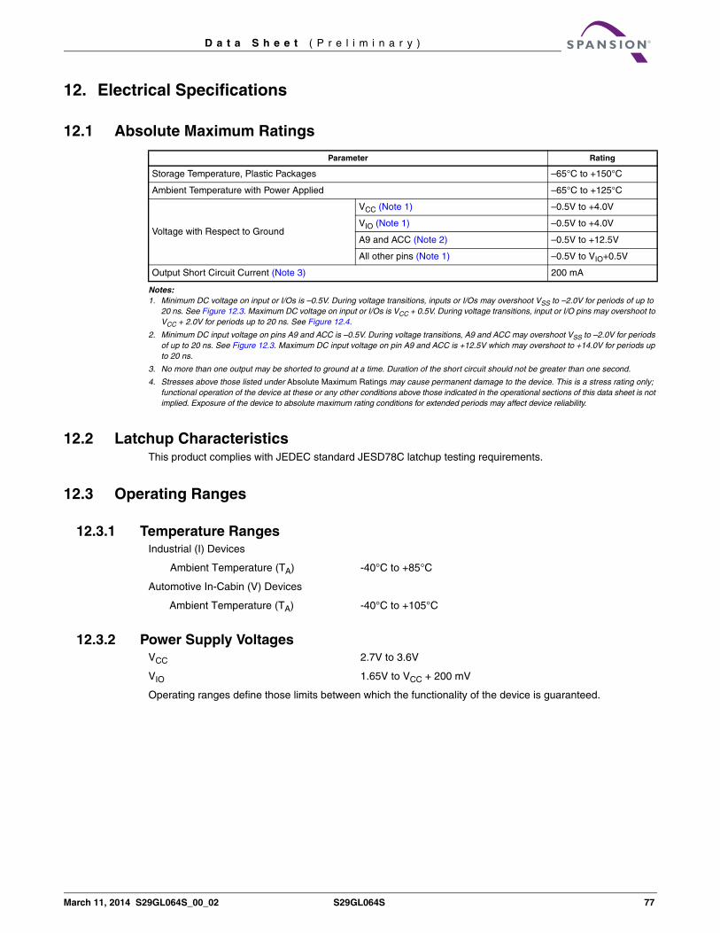
1. Product Selector GuideTable 1.1 Product Selector Guide for Industrial Temperature (-40°C to +85°C)
Table 1.2 Product Selector Guide for In Cabin Temperature (-40°C to +105°C)
Part Number S29GL064S
Speed Option VCC = 2.7–3.6VVIO = 2.7–3.6V 70
VIO = 1.65–3.6V 80
Max. Access Time (ns) 70 80
Max. CE# Access Time (ns) 70 80
Max. Page Access Time (ns) 15 25
Max. OE# Access Time (ns) 15 25
Part Number S29GL064S
Speed Option VCC = 2.7–3.6VVIO = 2.7–3.6V 80
VIO = 1.65–3.6V 90
Max. Access Time (ns) 80 90
Max. CE# Access Time (ns) 80 90
Max. Page Access Time (ns) 15 25
Max. OE# Access Time (ns) 15 25
March 11, 2014 S29GL064S_00_02 S29GL064S 11
D a t a S h e e t ( P r e l i m i n a r y )
2. Block Diagram
Notes:1. Available on separate pins for models 06, 07, V6, V7.
2. Available only on X8/x16 devices.
Input / OutputBuffers
X-Decoder
Y-Decoder
Chip EnableOutput Enable
Logic
Erase VoltageGenerator
PGM VoltageGenerator
TimerVCC Detector
StateControl
CommandRegister
VCC
VSS
WE#
WP#/ACC(1)
BYTE#(2)
CE#
OE#
STB
STB
DQ15–DQ0 (A-1)
Sector Switches
RY/BY#
RESET#
DataLatch
Y-Gating
Cell Matrix
Add
ress
Lat
ch
A21–A0
12 S29GL064S S29GL064S_00_02 March 11, 2014
D a t a S h e e t ( P r e l i m i n a r y )
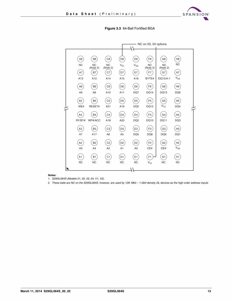
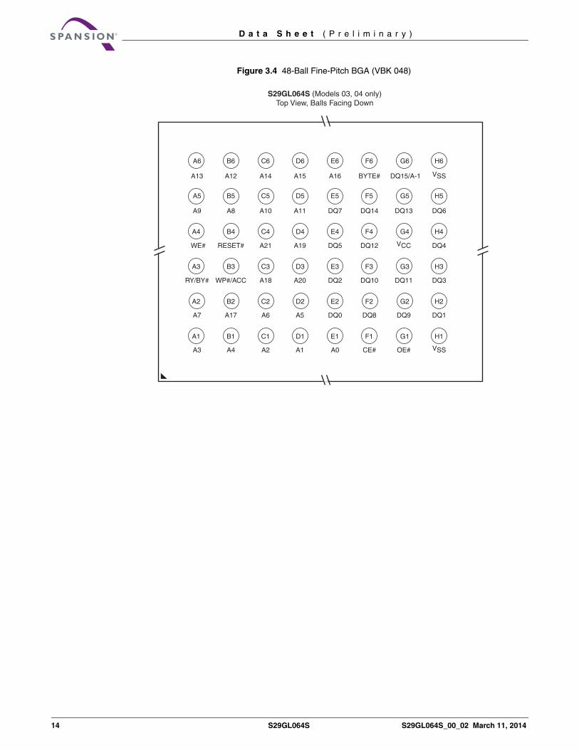
3. Connection Diagrams
Special Package Handling InstructionsSpecial handling is required for flash memory products in molded packages (TSOP and BGA). The package and/or data integrity may be compromised if the package body is exposed to temperatures above 150°C for prolonged periods of time.
Figure 3.1 48-Pin Standard TSOP
Figure 3.2 56-Pin Standard TSOP
Note:1. These pins are NC on the S29GL064S, however, are used by 128-Mbit –1-Gbit density GL devices as the high order address inputs.
VCC 3.0 volt-only single power supply (see Product Selector Guide on page 10 for speed options and voltage supply tolerances)
VIO Output Buffer Power
VSS Device Ground
NC Pin Not Connected Internally
RFUReserved for Future Use. Not currently connected internally but the pin/ball location should be left unconnected and unused by PCB routing channel for future compatibility. The pin/ball may be used by a signal in the future.
16 S29GL064S S29GL064S_00_02 March 11, 2014
D a t a S h e e t ( P r e l i m i n a r y )
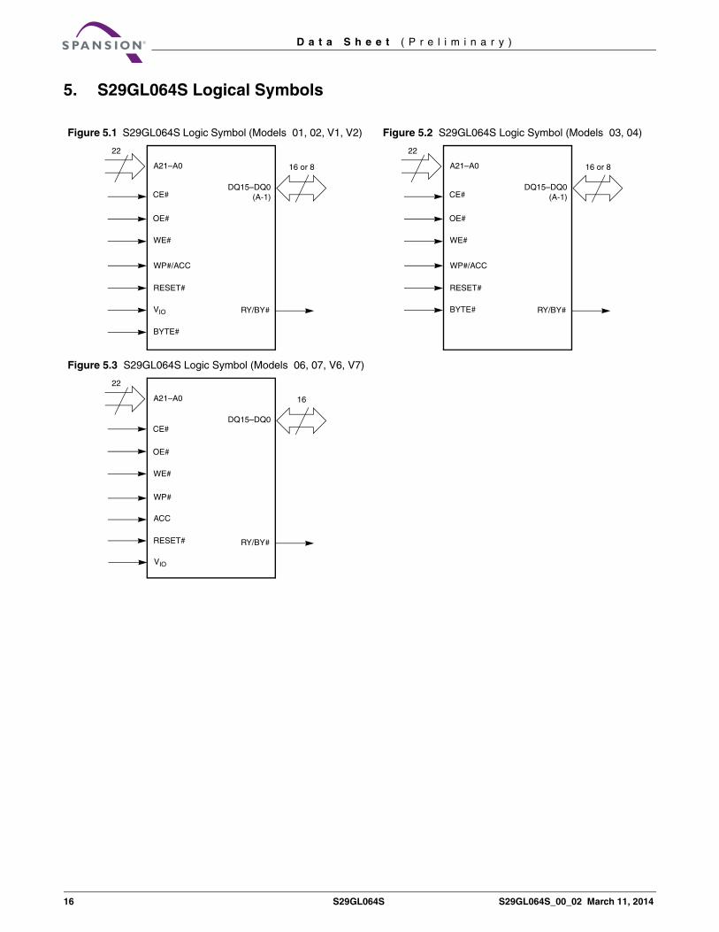
5. S29GL064S Logical Symbols
Figure 5.1 S29GL064S Logic Symbol (Models 01, 02, V1, V2) Figure 5.2 S29GL064S Logic Symbol (Models 03, 04)
Figure 5.3 S29GL064S Logic Symbol (Models 06, 07, V6, V7)
22
16 or 8
DQ15–DQ0(A-1)
A21–A0
CE#
OE#
WE#
RESET#
RY/BY#
WP#/ACC
VIO
BYTE#
22
16 or 8
DQ15–DQ0(A-1)
A21–A0
CE#
OE#
WE#
RESET#
RY/BY#
WP#/ACC
BYTE#
22
16
DQ15–DQ0
A21–A0
CE#
OE#
WE#
RESET# RY/BY#
WP#
ACC
VIO
March 11, 2014 S29GL064S_00_02 S29GL064S 17
D a t a S h e e t ( P r e l i m i n a r y )
6. Ordering Information – S29GL064S
6.1 S29GL064S Standard ProductsStandard products are available in several packages and operating ranges. The order number (Valid Combination) is formed by a combination of the following:
Device Number / DescriptionS29GL064S, 64-Megabit Page-Mode Flash Memory Manufactured using 65 nm MirrorBit Process Technology, 3.0 Volt-Only Read, Program, and Erase
18 S29GL064S S29GL064S_00_02 March 11, 2014
D a t a S h e e t ( P r e l i m i n a r y )
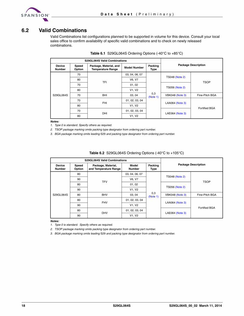
6.2 Valid CombinationsValid Combinations list configurations planned to be supported in volume for this device. Consult your local sales office to confirm availability of specific valid combinations and to check on newly released combinations.
Notes:1. Type 0 is standard. Specify others as required.
2. TSOP package marking omits packing type designator from ordering part number.
3. BGA package marking omits leading S29 and packing type designator from ordering part number.
Notes:1. Type 0 is standard. Specify others as required.
2. TSOP package marking omits packing type designator from ordering part number.
3. BGA package marking omits leading S29 and packing type designator from ordering part number.
Table 6.1 S29GL064S Ordering Options (-40°C to +85°C)
S29GL064S Valid Combinations
Package DescriptionDevice Number
Speed Option
Package, Material, and Temperature Range
Model NumberPacking
Type
S29GL064S
70
TFI
03, 04, 06, 07
0,3 (Note 1)
TS048 (Note 2)
TSOP80 V6, V7
70 01, 02TS056 (Note 2)
80 V1, V2
70 BHI 03, 04 VBK048 (Note 3) Fine-Pitch BGA
70 FHI
01, 02, 03, 04LAA064 (Note 3)
Fortified BGA80 V1, V2
70 DHI
01, 02, 03, 04LAE064 (Note 3)
80 V1, V2
Table 6.2 S29GL064S Ordering Options (-40°C to +105°C)
S29GL064S Valid Combinations
Package DescriptionDeviceNumber
SpeedOption
Package, Material,and Temperature Range
ModelNumber
PackingType
S29GL064S
80
TFV
03, 04, 06, 07
0,3 (Note 1)
TS048 (Note 2)
TSOP90 V6, V7
80 01, 02TS056 (Note 2)
90 V1, V2
80 BHV 03, 04 VBK048 (Note 3) Fine-Pitch BGA
80 FHV
01, 02, 03, 04LAA064 (Note 3)
Fortified BGA90 V1, V2
80 DHV
01, 02, 03, 04LAE064 (Note 3)
90 V1, V2
March 11, 2014 S29GL064S_00_02 S29GL064S 19
D a t a S h e e t ( P r e l i m i n a r y )
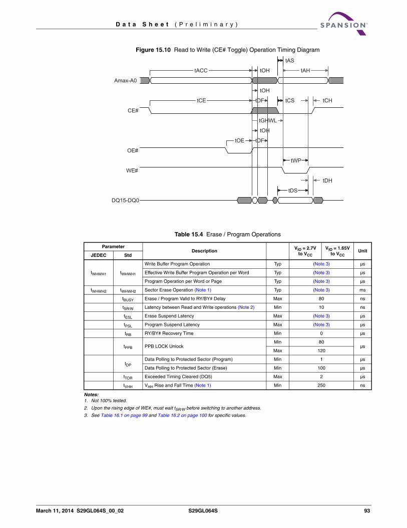
7. Device Bus OperationsThis section describes the requirements and use of the device bus operations, which are initiated through the internal command register. The command register itself does not occupy any addressable memory location. The register is a latch used to store the commands, along with the address and data information needed to execute the command. The contents of the register serve as inputs to the internal state machine. The state machine outputs dictate the function of the device. Table 7.1 lists the device bus operations, the inputs and control levels they require, and the resulting output. The following subsections describe each of these operations in further detail.
Legend:L = Logic Low = VIL
H = Logic High = VIH
VHH = Voltage for ACC Program AccelerationVID = Voltage for AutoselectX = Don’t CareAIN = Address InDIN = Data InDOUT = Data Out
Notes:1. If WP# = VIL, the first or last sector remains protected (for uniform sector devices), and the two outer boot sectors are protected (for boot sector devices).
If WP# = VIH, the first or last sector, or the two outer boot sectors are protected or unprotected as determined by the method described in Write Protect (WP#). All sectors are unprotected when shipped from the factory (The Secure Silicon Region may be factory protected depending on version ordered.)
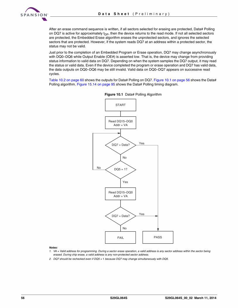
2. DIN or DOUT as required by command sequence, data polling, or sector protect algorithm (see Figure 10.1 on page 56).
3. A9 is raised to VID to enable Autoselect reads.
4. VIL = VSS and VIH = VIO.
7.1 Word / Byte ConfigurationThe BYTE# pin controls whether the device data I/O pins operate in the byte or word configuration. If the BYTE# pin is set at logic 1, the device is in word configuration, DQ0–DQ15 are active and controlled by CE#, WE# and OE#.
If the BYTE# pin is set at logic 0, the device is in byte configuration, and only data I/O pins DQ0–DQ7 are active and controlled by CE#, WE# and OE#. The data I/O pins DQ8–DQ14 are tri-stated, and the DQ15 pin is used as an input for the LSB (A-1) address function.
The BYTE# pin must be driven set to a logic 0 or 1 state prior to CE# being driven low. The BYTE# pin should not change logic state while CE# is low.
Accelerated Program L H L H L or H (Note 1) VHH AIN (Note 2) (Note 2)
Standby VIO ± 0.3V X X VIO ± 0.3V L or H X H X High-Z High-Z High-Z
Output DisableL H H
H L or H X X X High-Z High-Z High-ZH X X
Reset X X X L L or H X X X High-Z High-Z High-Z
20 S29GL064S S29GL064S_00_02 March 11, 2014
D a t a S h e e t ( P r e l i m i n a r y )
7.2 Requirements for Reading Array DataAll memories require access time to output array data. In a read operation, data is read from one memory location at a time. Addresses are presented to the device in random order, and the propagation delay through the device causes the data on its outputs to arrive with the address on its inputs.
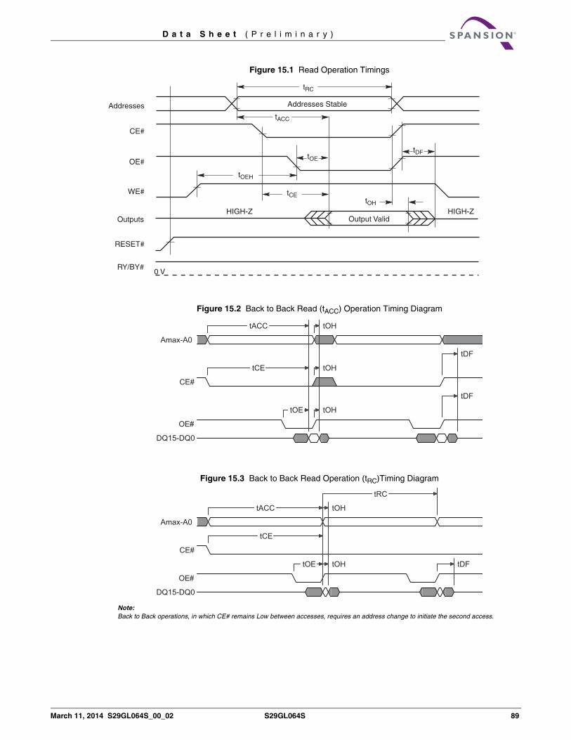
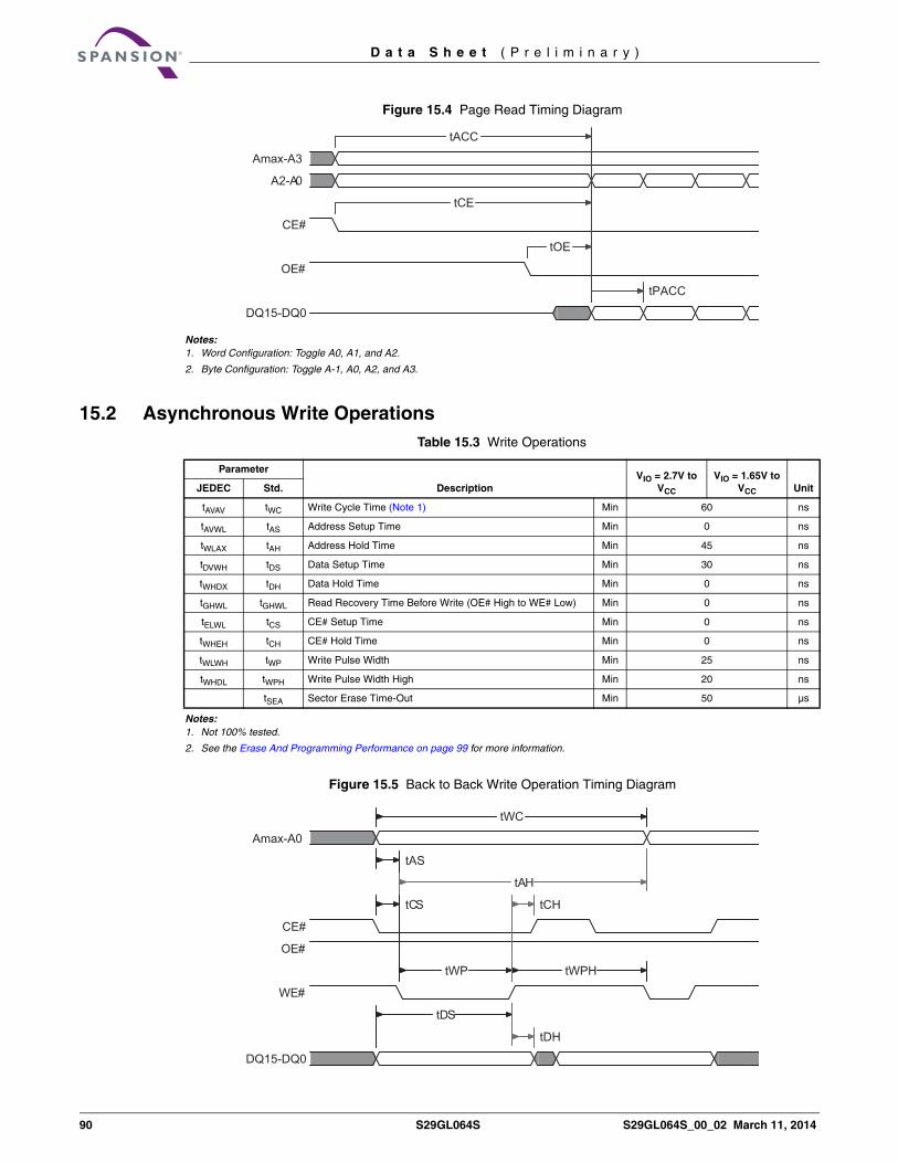
The device defaults to reading array data after device power-up or hardware reset. To read data from the memory array, the system must first assert a valid address on Amax-A0, while driving OE# and CE# to VIL. WE# must remain at VIH. Data will appear on DQ15-DQ0 after address access time (tACC), which is equal to the delay from stable addresses to valid output data. The OE# signal must be driven to VIL. Data is output on DQ15-DQ0 pins after the access time (tOE) has elapsed from the falling edge of OE#.
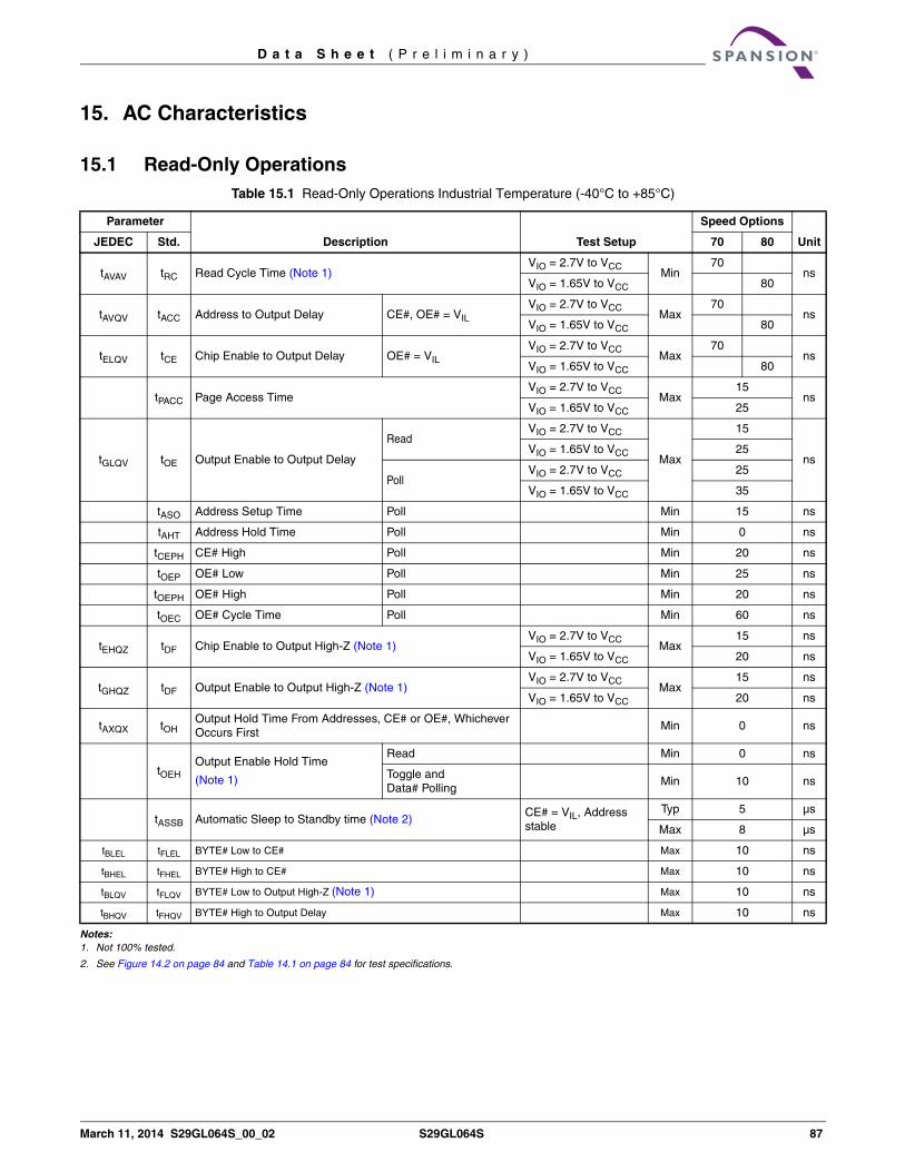
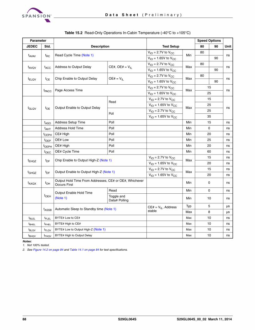
See Reading Array Data on page 35 for more information. Refer to Table 15.1 on page 87 and Table 15.2 on page 88 for timing specifications and the timing diagram. Refer to Table 13.1 on page 81 and Table 13.2 on page 82 for the active current specification on reading array data.
7.2.1 Page Mode ReadThe device is capable of fast page mode read and is compatible with the page mode Mask ROM read operation. This mode provides faster read access speed for random locations within a page. The page size of the device is 8 words / 16 bytes. The appropriate page is selected by the higher address bits A(max)–A3. Address bits A2–A0 in word mode (A2–A-1 in byte mode) determine the specific word within a page. This is an asynchronous operation; the microprocessor supplies the specific word location.
The random or initial page access is equal to tACC or tCE and subsequent page read accesses (as long as the locations specified by the microprocessor falls within that page) is equivalent to tPACC. When CE# is deasserted and reasserted for a subsequent access, the access time is tACC or tCE. Fast page mode accesses are obtained by keeping the read-page addresses constant and changing the intra-read page addresses.
7.3 Writing Commands / Command SequencesTo write a command or command sequence (which includes programming data to the device and erasing sectors of memory), the system must drive WE# and CE# to VIL, and OE# to VIH.
The device features an Unlock Bypass mode to facilitate faster programming. Once the device enters the Unlock Bypass mode, only two write cycles are required to program a word, instead of four. The Word Program Command Sequence on page 36 contains details on programming data to the device using both standard and Unlock Bypass command sequences.
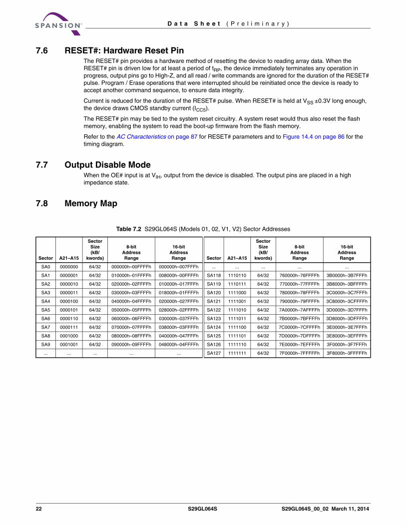
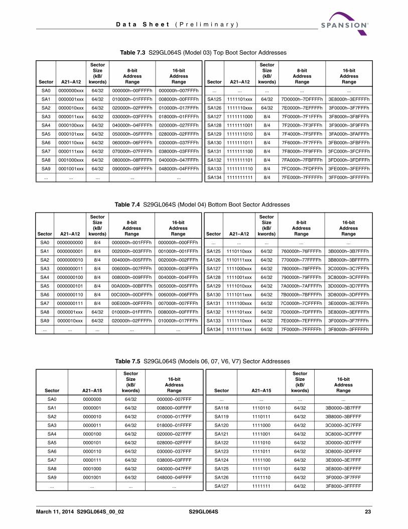
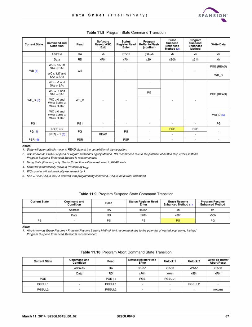
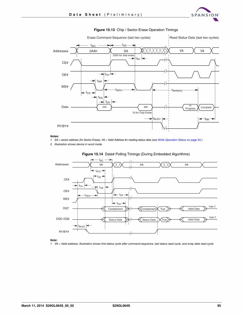
An erase operation can erase one sector, multiple sectors, or the entire device. Tables 7.2 – 7.5 indicate the address space that each sector occupies.
Refer to DC Characteristics on page 81 for the active current specification for the write mode. The AC Characteristics section contains timing specification tables and timing diagrams for write operations.
7.3.1 Write BufferWrite Buffer Programming allows the system write to a maximum of 128 words / 256 bytes in one programming operation. This results in faster effective programming time than the standard programming algorithms.
March 11, 2014 S29GL064S_00_02 S29GL064S 21
D a t a S h e e t ( P r e l i m i n a r y )
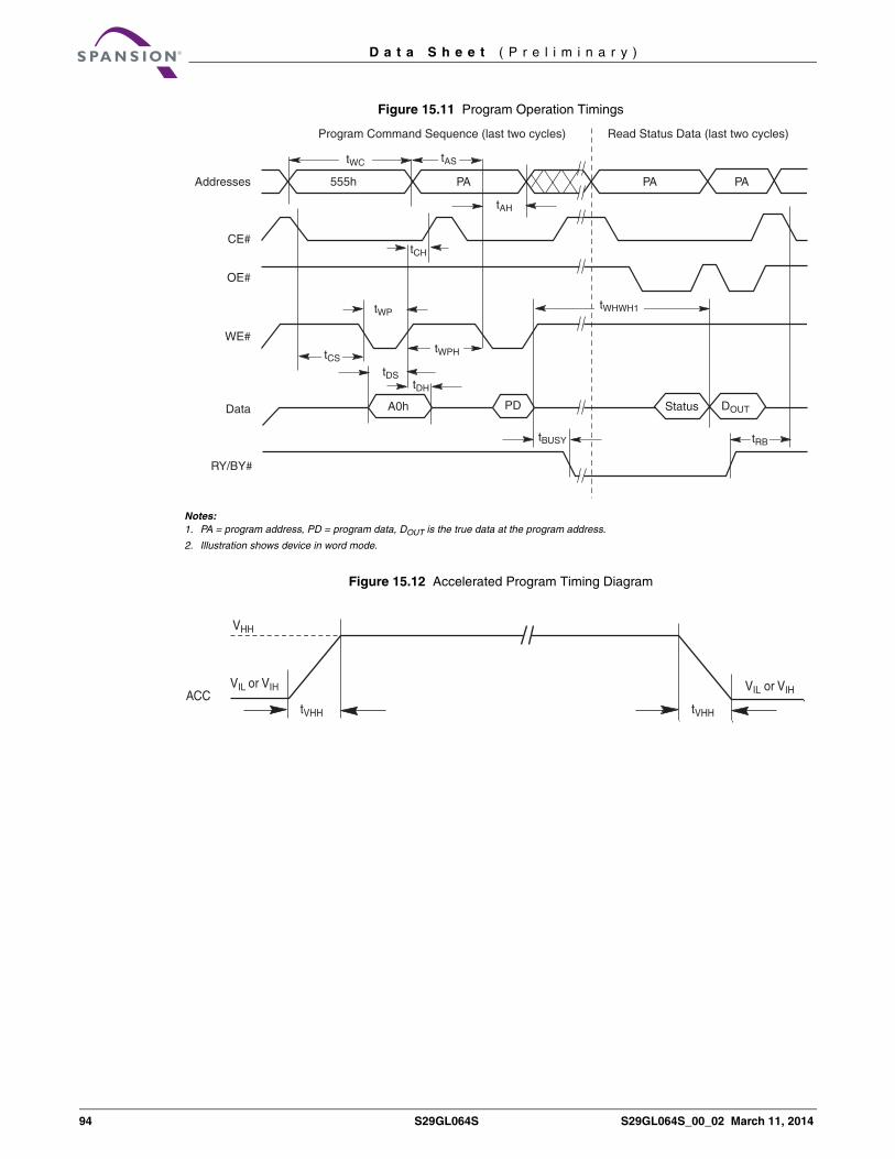
7.3.2 Accelerated Program OperationThe device offers program operations through the ACC function. This is one of two functions provided by the WP#/ACC or ACC pin, depending on model number. This function is primarily intended to support manufacturing programming operations at the factory.
If the system asserts VHH on this pin, the device automatically enters the Unlock Bypass mode, protected sectors will remain protected. The system would use a two-cycle program command sequence as required by the Unlock Bypass mode. Removing VHH from the WP#/ACC or ACC pin, depending on model number, returns the device to normal operation. Note that the WP#/ACC or ACC pin must be raised to VHH prior to any accelerated operation and should return to VIL/VIH after the completion of the accelerated operation. It should not be at VHH for operations other than accelerated programming, or device damage may result. WP# contains an internal pull-up; when unconnected, WP# is at VIH.
7.3.3 Autoselect FunctionsIf the system writes the autoselect command sequence, the device enters the autoselect mode. The system can then read autoselect codes from the internal register (which is separate from the memory array) on DQ7-DQ0. Standard read cycle timings (tACC) apply in this mode. Refer to Autoselect Mode on page 24 and Autoselect Command Sequence on page 36 for more information.
7.4 Standby ModeWhen the system is not reading or writing to the device, it can be placed in to standby mode. In this mode, current consumption is greatly reduced, and the outputs are placed in the high impedance state, independent of the OE# input.
The device enters the CMOS standby mode when the CE# and RESET# pins are both held at VIO ± 0.3V. (Note that this is a more restricted voltage range than VIH.) If CE# and RESET# are held at VIH, but not within VIO ± 0.3V, the device is in the standby mode, but the standby current is greater. The device requires standard access time (tACC/tCE) for read access when the device is in either of these standby modes, before it is ready to read data.
If the device is deselected during erasure or programming, the device draws active current until the operation is completed.
Refer to the DC Characteristics on page 81, for the standby current specification.
7.5 Automatic Sleep ModeThe automatic sleep mode reduces device interface energy consumption to the sleep level (ICC6) following the completion of a random read access time. The device automatically enables this mode when addresses remain stable for tACC + 30 ns. While in sleep mode, output data is latched and always available to the system. Output of the data depends on the level of the OE# signal but, the automatic sleep mode current is independent of the OE# signal level. Standard address access timings (tACC or tPACC) provide new data when addresses are changed. Refer to the DC Characteristics on page 81 for the automatic sleep mode current specification ICC6.
Automatic sleep helps reduce current consumption especially when the host system clock is slowed for power reduction. During slow system clock periods, read and write cycles may extend many times their length versus when the system is operating at high speed. Even though CE# may be Low throughout these extended data transfer cycles, the memory device host interface will go to the Automatic Sleep current at tACC + 30 ns. The device will remain at the Automatic Sleep current for tASSB. Then the device will transition to the standby current level. This keeps the memory at the Automatic Sleep or standby power level for most of the long duration data transfer cycles, rather than consuming full read power all the time that the memory device is selected by the host system.
However, the EAC operates independent of the automatic sleep mode of the host interface and will continue to draw current during an active Embedded Algorithm. Only when both the host interface and EAC are in their standby states is the standby level current achieved.
22 S29GL064S S29GL064S_00_02 March 11, 2014
D a t a S h e e t ( P r e l i m i n a r y )
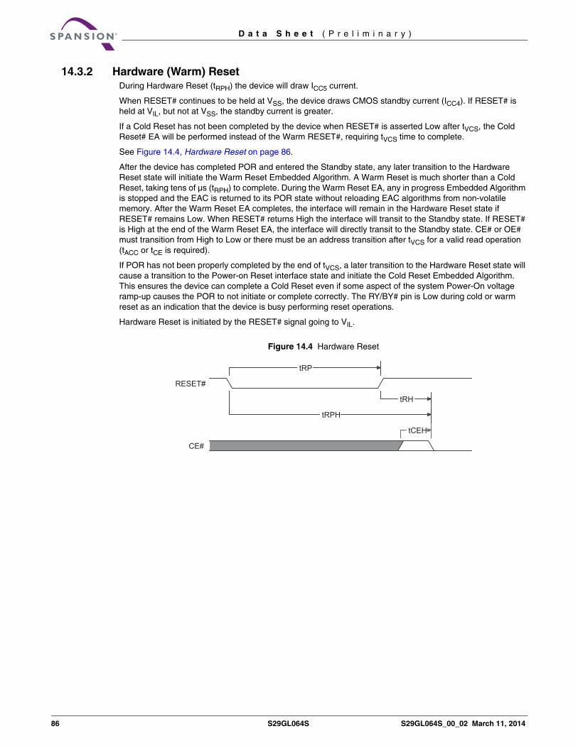
7.6 RESET#: Hardware Reset PinThe RESET# pin provides a hardware method of resetting the device to reading array data. When the RESET# pin is driven low for at least a period of tRP, the device immediately terminates any operation in progress, output pins go to High-Z, and all read / write commands are ignored for the duration of the RESET# pulse. Program / Erase operations that were interrupted should be reinitiated once the device is ready to accept another command sequence, to ensure data integrity.
Current is reduced for the duration of the RESET# pulse. When RESET# is held at VSS ±0.3V long enough, the device draws CMOS standby current (ICC5).
The RESET# pin may be tied to the system reset circuitry. A system reset would thus also reset the flash memory, enabling the system to read the boot-up firmware from the flash memory.
Refer to the AC Characteristics on page 87 for RESET# parameters and to Figure 14.4 on page 86 for the timing diagram.
7.7 Output Disable ModeWhen the OE# input is at VIH, output from the device is disabled. The output pins are placed in a high impedance state.
7.9 Autoselect ModeThe autoselect mode provides manufacturer and device identification, and sector protection verification, through identifier codes output on DQ7–DQ0. This mode is primarily intended for programming equipment to automatically match a device to be programmed with its corresponding programming algorithm. However, the autoselect codes can also be accessed in-system through the command register.
When using programming equipment, the autoselect mode requires VID on address pin A9. Address pins A6, A3, A2, A1, and A0 must be as shown in Table 7.6 on page 24. In addition, when verifying sector protection, the sector address must appear on the appropriate highest order address bits (see Table 7.2 - 7.5). Table 7.6 shows the remaining address bits that are don’t care. When all necessary bits are set as required, the programming equipment may then read the corresponding identifier code on DQ7–DQ0. Note that the A9 pin must not be at VID for operations other than Autoselect, or device damage may result. Autoselect using VID is supported at room temperature only. It must be raised to VID prior to any autoselect operations and should return to VIL/VIH after the completion of the autoselect operation. It should not be at VID for operations other than autoselect, or device damage may result.
To access the autoselect codes in-system, the host system can issue the autoselect command via the command register, as shown in Table 9.3 on page 46 and Table 9.5 on page 50. This method does not require VID. Refer to the Autoselect Command Sequence on page 36 for more information.
ID-CFI Location 02h displays sector protection status for the sector selected by the sector address (SA) used in the ID-CFI enter command. To read the protection status of more than one sector it is necessary to exit the ID ASO and enter the ID ASO using the new SA. The access time to read location 02h is always tACC and a read of this location requires CE# to go High before the read and return Low to initiate the read (asynchronous read access). Page mode read between location 02h and other ID locations is not supported. Page mode read between ID locations other than 02h is supported.
In x8 mode, address A-1 is ignored and the lower 8 bits of data will be returned for both address.
Legend:L = Logic Low = VIL
H = Logic High = VIH
SA = Sector AddressX = Don’t care
Table 7.6 Autoselect Codes, (High Voltage Method)
Description CE# OE# WE#
Amax to
A15
A14to
A10 A9
A8toA7 A6
A5 to A4
A3toA2 A1 A0
DQ8 to DQ15
DQ7 to DQ0
Model Number
BYTE#= VIH
BYTE#= VIL
01, 02V1, V2 03, 04
06, 07,V6, V7
Manufacturer ID:Spansion Products
L L H X X VID X L X L L L 00 X 01h 01h 01h
S29
GL0
64S
Cycle 1
L L H X X VID X L X
L L H 22 X 7Eh 7Eh 7Eh
Cycle 2 H H L 22 X 0Ch 10h 13h
Cycle 3 H H H 22 X 01h00h (04, bottom
boot)01h (03, top boot)
01h
Sector Protection Verification
L L H SA X VID X L X L H L X X01h (protected),
00h (unprotected)
Secure Silicon Region Indicator Bit (DQ7), WP# protects highest address sector
L L H X X VID X L X L H H X X9A (factory locked),
1A (not factory locked)
Secure Silicon Region Indicator Bit (DQ7), WP# protects lowest address sector
L L H X X VID X L X L H H X X8A (factory locked),
0A (not factory locked)
March 11, 2014 S29GL064S_00_02 S29GL064S 25
D a t a S h e e t ( P r e l i m i n a r y )
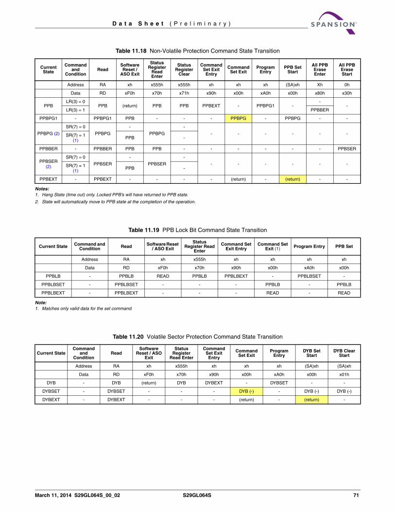
7.10 Advanced Sector ProtectionThe device features several levels of sector protection, which can disable both the program and erase operations in certain sectors.
7.10.1 Persistent Sector ProtectionA command sector protection method that replaces the old 12V controlled protection method.
7.10.2 Password Sector ProtectionA highly sophisticated protection method that requires a password before changes to certain sectors are permitted.
7.10.3 WP# Hardware ProtectionA write protect pin that can prevent program or erase operations in the outermost sectors.
The WP# Hardware Protection feature is always available, independent of the software managed protection method chosen.
7.10.4 Selecting a Sector Protection ModeAll parts default to operate in the Persistent Sector Protection mode. The user must then choose if the Persistent or Password Protection method is most desirable. There are two one-time programmable non-volatile bits that define which sector protection method is used. If the user decides to continue using the Persistent Sector Protection method, they must set the Persistent Sector Protection Mode Locking Bit. This permanently sets the part to operate only using Persistent Sector Protection. If the user decides to use the password method, they must set the Password Mode Locking Bit. This permanently sets the part to operate only using password sector protection.
It is important to remember that setting either the Persistent Sector Protection Mode Locking Bit or the Password Mode Locking Bit permanently selects the protection mode. It is not possible to switch between the two methods once a locking bit is set. It is important that one mode is explicitly selected when the device is first programmed, rather than relying on the default mode alone. This is so that it is not possible for a system program or virus to later set the Password Mode Locking Bit, which would cause an unexpected shift from the default Persistent Sector Protection Mode into the Password Protection Mode.
The device is shipped with all sectors unprotected. Spansion offers the option of programming and protecting sectors at the factory prior to shipping the device through the ExpressFlash™ Service. Contact your sales representative for details.
It is possible to determine whether a sector is protected or unprotected. See Autoselect Command Sequence on page 36 for details.
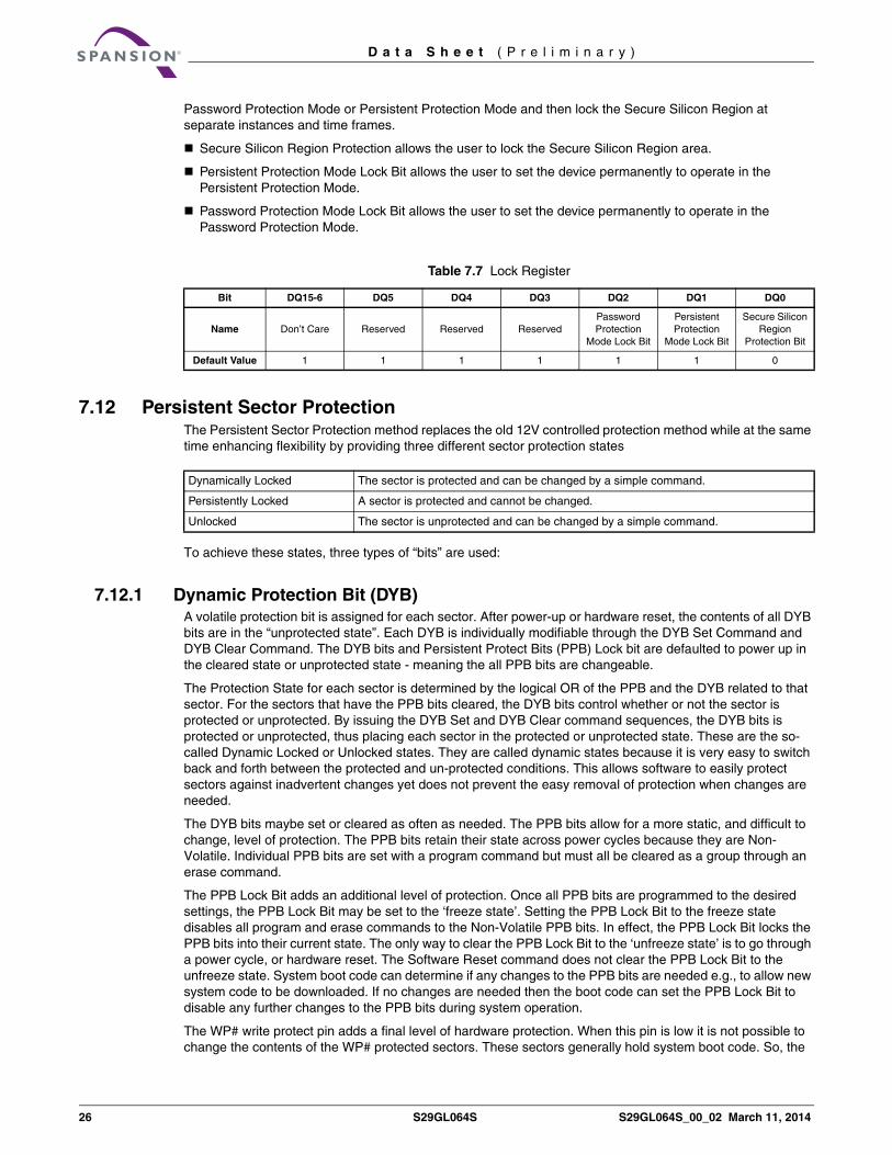
7.11 Lock RegisterThe Lock Register consists of 3 bits (DQ2, DQ1, and DQ0). These DQ2, DQ1, DQ0 bits of the Lock Register are programmable by the user. Users are not allowed to program both DQ2 and DQ1 bits of the Lock Register to the 00 state. If the user tries to program DQ2 and DQ1 bits of the Lock Register to the 00 state, the device aborts the Lock Register back to the default 11 state. Once either DQ2 and DQ1 bits of the Lock Register are programmed than no further changes are allow on DQ2 and DQ1. The programming time of the Lock Register is same as the typical word programming time (tWHWH1) without utilizing the Write Buffer of the device. During a Lock Register programming sequence execution, the DQ6 Toggle Bit I toggles until the programming of the Lock Register has completed to indicate programming status. All Lock Register bits are readable to allow users to verify Lock Register statuses.
The Customer Secure Silicon Region Protection Bit is DQ0, Persistent Protection Mode Lock Bit is DQ1, and Password Protection Mode Lock Bit is DQ2 are accessible by all users. Each of these bits are non-volatile. DQ15-DQ3 are reserved and must be 1's when the user tries to program the DQ2, DQ1, and DQ0 bits of the Lock Register. The user is not required to program DQ2, DQ1 and DQ0 bits of the Lock Register at the same time. This allows users to lock the Secure Silicon Region and then set the device either permanently into
26 S29GL064S S29GL064S_00_02 March 11, 2014
D a t a S h e e t ( P r e l i m i n a r y )
Password Protection Mode or Persistent Protection Mode and then lock the Secure Silicon Region at separate instances and time frames.
Secure Silicon Region Protection allows the user to lock the Secure Silicon Region area.
Persistent Protection Mode Lock Bit allows the user to set the device permanently to operate in the Persistent Protection Mode.
Password Protection Mode Lock Bit allows the user to set the device permanently to operate in the Password Protection Mode.
7.12 Persistent Sector ProtectionThe Persistent Sector Protection method replaces the old 12V controlled protection method while at the same time enhancing flexibility by providing three different sector protection states
To achieve these states, three types of “bits” are used:
7.12.1 Dynamic Protection Bit (DYB) A volatile protection bit is assigned for each sector. After power-up or hardware reset, the contents of all DYB bits are in the “unprotected state”. Each DYB is individually modifiable through the DYB Set Command and DYB Clear Command. The DYB bits and Persistent Protect Bits (PPB) Lock bit are defaulted to power up in the cleared state or unprotected state - meaning the all PPB bits are changeable.
The Protection State for each sector is determined by the logical OR of the PPB and the DYB related to that sector. For the sectors that have the PPB bits cleared, the DYB bits control whether or not the sector is protected or unprotected. By issuing the DYB Set and DYB Clear command sequences, the DYB bits is protected or unprotected, thus placing each sector in the protected or unprotected state. These are the so-called Dynamic Locked or Unlocked states. They are called dynamic states because it is very easy to switch back and forth between the protected and un-protected conditions. This allows software to easily protect sectors against inadvertent changes yet does not prevent the easy removal of protection when changes are needed.
The DYB bits maybe set or cleared as often as needed. The PPB bits allow for a more static, and difficult to change, level of protection. The PPB bits retain their state across power cycles because they are Non-Volatile. Individual PPB bits are set with a program command but must all be cleared as a group through an erase command.
The PPB Lock Bit adds an additional level of protection. Once all PPB bits are programmed to the desired settings, the PPB Lock Bit may be set to the ‘freeze state’. Setting the PPB Lock Bit to the freeze state disables all program and erase commands to the Non-Volatile PPB bits. In effect, the PPB Lock Bit locks the PPB bits into their current state. The only way to clear the PPB Lock Bit to the ‘unfreeze state’ is to go through a power cycle, or hardware reset. The Software Reset command does not clear the PPB Lock Bit to the unfreeze state. System boot code can determine if any changes to the PPB bits are needed e.g., to allow new system code to be downloaded. If no changes are needed then the boot code can set the PPB Lock Bit to disable any further changes to the PPB bits during system operation.
The WP# write protect pin adds a final level of hardware protection. When this pin is low it is not possible to change the contents of the WP# protected sectors. These sectors generally hold system boot code. So, the
Table 7.7 Lock Register
Bit DQ15-6 DQ5 DQ4 DQ3 DQ2 DQ1 DQ0
Name Don’t Care Reserved Reserved ReservedPassword Protection
Mode Lock Bit
Persistent Protection
Mode Lock Bit
Secure Silicon Region
Protection Bit
Default Value 1 1 1 1 1 1 0
Dynamically Locked The sector is protected and can be changed by a simple command.
Persistently Locked A sector is protected and cannot be changed.
Unlocked The sector is unprotected and can be changed by a simple command.
March 11, 2014 S29GL064S_00_02 S29GL064S 27
D a t a S h e e t ( P r e l i m i n a r y )
WP# pin can prevent any changes to the boot code that could override the choices made while setting up sector protection during system initialization.
It is possible to have sectors that have been persistently locked, and sectors that are left in the dynamic state. The sectors in the dynamic state are all unprotected. If there is a need to protect some of them, a simple DYB Set command sequence is all that is necessary. The DYB Set and DYB Clear commands for the dynamic sectors switch the DYB bits to signify protected and unprotected, respectively. If there is a need to change the status of the persistently locked sectors, a few more steps are required. First, the PPB Lock Bit must be disabled to the unfreeze state by either putting the device through a power-cycle, or hardware reset. The PPB bits can then be changed to reflect the desired settings. Setting the PPB Lock Bit once again to the freeze state locks the PPB bits, and the device operates normally again.
To achieve the best protection, execute the PPB Lock Bit Set command early in the boot code, and protect the boot code by holding WP# = VIL.
7.12.2 Persistent Protection Bit (PPB) A single Persistent (non-volatile) Protection Bit is assigned to each sector. If a PPB is programmed to the protected state through the PPB Program command, that sector is protected from program or erase operations and is therefor read-only. If a PPB requires erasure, all of the sector PPB bits must first be erased in parallel through the All PPB Erase command. The All PPB Erase command preprograms all PPB bits prior to PPB erasing. All PPB bits erase in parallel, unlike programming where individual PPB bits are programmable. The PPB bits are limited to the same number of cycles as a flash memory sector.
Programming the PPB bit requires the typical word programming time without utilizing the Write Buffer. During a PPB bit programming and all PPB bit erasing sequence executions, the DQ6 Toggle Bit I toggles until the programming of the PPB bit or erasing of all PPB bits has completed to indicate programming and erasing status. Erasing all of the PPB bits at once requires typical sector erase time. During the erasing of all PPB bits, the DQ3 Sector Erase Timer bit outputs a 1 to indicate the erasure of all PPB bits are in progress. Reading the PPB Status bit requires the initial access time of the device.
7.12.3 Persistent Protection Bit Lock (PPB Lock Bit) A global volatile bit. When set to the freeze state, the PPB bits cannot be changed. When cleared to the unfreeze state, the PPB bits are changeable. There is only one PPB Lock Bit per device. The PPB Lock Bit is cleared to the unfreeze state at power-up or hardware reset.
Configuring the PPB Lock Bit to the freeze state requires approximately tWC. Reading the PPB Lock Status bit requires the initial access time (tACC) of the device.
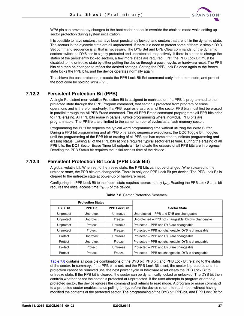
Table 7.8 contains all possible combinations of the DYB bit, PPB bit, and PPB Lock Bit relating to the status of the sector. In summary, if the PPB bit is set, and the PPB Lock Bit is set, the sector is protected and the protection cannot be removed until the next power cycle or hardware reset clears the PPB Lock Bit to unfreeze state. If the PPB bit is cleared, the sector can be dynamically locked or unlocked. The DYB bit then controls whether or not the sector is protected or unprotected. If the user attempts to program or erase a protected sector, the device ignores the command and returns to read mode. A program or erase command to a protected sector enables status polling for tDP before the device returns to read mode without having modified the contents of the protected sector. The programming of the DYB bit, PPB bit, and PPB Lock Bit for
Table 7.8 Sector Protection Schemes
Protection States
Sector StateDYB Bit PPB Bit PPB Lock Bit
Unprotect Unprotect Unfreeze Unprotected – PPB and DYB are changeable
Unprotect Unprotect Freeze Unprotected – PPB not changeable, DYB is changeable
Unprotect Protect Unfreeze Protected – PPB and DYB are changeable
Unprotect Protect Freeze Protected – PPB not changeable, DYB is changeable
Protect Unprotect Unfreeze Protected – PPB and DYB are changeable
Protect Unprotect Freeze Protected – PPB not changeable, DYB is changeable
Protect Protect Unfreeze Protected – PPB and DYB are changeable
Protect Protect Freeze Protected – PPB not changeable, DYB is changeable
28 S29GL064S S29GL064S_00_02 March 11, 2014
D a t a S h e e t ( P r e l i m i n a r y )
a given sector can be verified by writing a DYB Status Read, PPB Status Read, and PPB Lock Status Read commands to the device.
The Autoselect Sector Protection Verification outputs the OR function of the DYB bit and PPB bit per sector basis. When the OR function of the DYB bit and PPB bit is a 1, the sector is either protected by DYB or PPB or both. When the OR function of the DYB bit and PPB bit is a 0, the sector is unprotected through both the DYB and PPB.
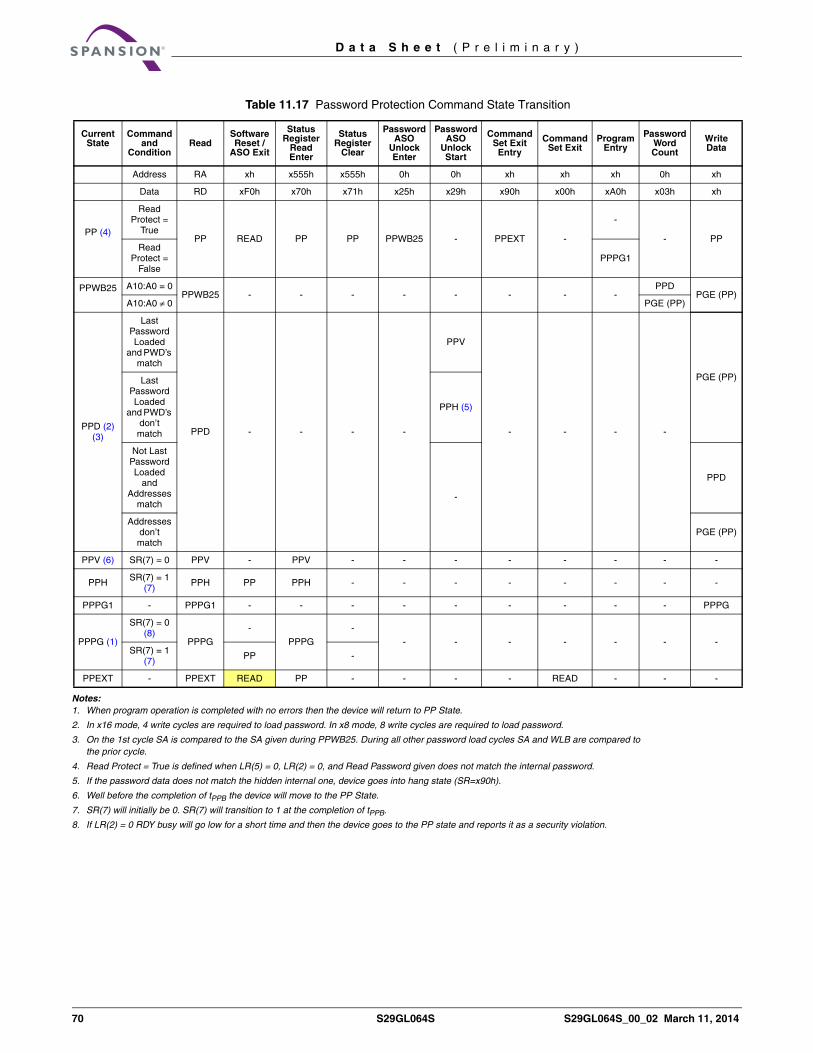
7.13 Password Sector ProtectionThe Password Sector Protection method allows an even higher level of security than the Persistent Sector Protection method. There are two main differences between the Persistent Sector Protection and the Password Sector Protection methods:
When the device is first powered on, or comes out of a reset cycle, the PPB Lock Bit is set to the locked state, or the freeze state, rather than cleared to the unlocked state, or the unfreeze state.
The only means to clear and unfreeze the PPB Lock Bit is by writing a unique 64-bit Password to the device.
The Password Sector Protection method is otherwise identical to the Persistent Sector Protection method.
A 64-bit password is the only additional tool utilized in this method.
The password is stored in a one-time programmable (OTP) region outside of the flash memory. Once the Password Protection Mode Lock Bit is set, the password is permanently set with no means to read, program, or erase it. The password is used to clear and unfreeze the PPB Lock Bit. The Password Unlock command must be written to the flash, along with a password. The flash device internally compares the given password with the pre-programmed password. If they match, the PPB Lock Bit is cleared to the unfreezed state, and the PPB bits can be altered. If they do not match, the flash device does nothing. There is a built-in tPPB delay for each password check after the valid 64-bit password is entered for the PPB Lock Bit to be cleared to the unfreezed state. This delay is intended to thwart any efforts to run a program that tries all possible combinations in order to crack the password.
7.14 Password and Password Protection Mode Lock Bit In order to select the Password Sector Protection method, the user must first program the password. Spansion recommends that the password be somehow correlated to the unique Electronic Serial Number (ESN) of the particular flash device. Each ESN is different for every flash device; therefore each password should be different for every flash device. While programming in the password region, the customer may perform Password Read operations. Once the desired password is programmed in, the customer must then set the Password Protection Mode Lock Bit. This operation achieves two objectives:
1. It permanently sets the device to operate using the Password Protection Mode. It is not possible to reverse this function.
2. It also disables all further commands to the password region. All program, and read operations are ignored.
Both of these objectives are important, and if not carefully considered, may lead to unrecoverable errors. The user must be sure that the Password Sector Protection method is desired when programming the Password Protection Mode Lock Bit. More importantly, the user must be sure that the password is correct when the Password Protection Mode Lock Bit is programmed. Due to the fact that read operations are disabled, there is no means to read what the password is afterwards. If the password is lost after programming the Password Protection Mode Lock Bit, there is no way to clear and unfreeze the PPB Lock Bit. The Password Protection Mode Lock Bit, once programmed, prevents reading the 64-bit password on the DQ bus and further password programming. The Password Protection Mode Lock Bit is not erasable. Once Password Protection Mode Lock Bit is programmed, the Persistent Protection Mode Lock Bit is disabled from programming, guaranteeing that no changes to the protection scheme are allowed.
March 11, 2014 S29GL064S_00_02 S29GL064S 29
D a t a S h e e t ( P r e l i m i n a r y )
7.14.1 64-Bit PasswordThe 64-bit password is located in its own memory space and is accessible through the use of the Password Program and Password Read commands. The password function works in conjunction with the Password Protection Mode Lock Bit, which when programmed, prevents the Password Read command from reading the contents of the password on the pins of the device.
7.15 Persistent Protection Bit Lock (PPB Lock Bit) A global volatile bit. The PPB Lock Bit is a volatile bit that reflects the state of the Password Protection Mode Lock Bit after power-up reset. If the Password Protection Mode Lock Bit is also programmed after programming the Password, the Password Unlock command must be issued to clear and unfreeze the PPB Lock Bit after a hardware reset (RESET# asserted) or a power-up reset. Successful execution of the Password Unlock command clears and unfreezes the PPB Lock Bit, allowing for sector PPB bits to be modified. Without issuing the Password Unlock command, while asserting RESET#, taking the device through a power-on reset, or issuing the PPB Lock Bit Set command sets the PPB Lock Bit to a the freeze state.
If the Password Protection Mode Lock Bit is not programmed, the device defaults to Persistent Protection Mode. In the Persistent Protection Mode, the PPB Lock Bit is cleared to the unfreeze state after power-up or hardware reset. The PPB Lock Bit is set to the freeze state by issuing the PPB Lock Bit Set command. Once set to the freeze state the only means for clearing the PPB Lock Bit to the unfreeze state is by issuing a hardware or power-up reset. The Password Unlock command is ignored in Persistent Protection Mode.
Reading the PPB Lock Bit requires the initial access time (tACC) of the device.
7.16 Secure Silicon Region Flash MemoryThe Secure Silicon Region feature provides a flash memory region that enables permanent part identification through an Electronic Serial Number (ESN). The Secure Silicon Region is 256 bytes in length, and uses a Secure Silicon Region Indicator Bit (DQ7) in Autoselect Mode to indicate whether or not the Secure Silicon Region is locked when shipped from the factory. This bit is permanently set at the factory and cannot be changed, which prevents cloning of a factory locked part. This ensures the security of the ESN once the product is shipped to the field.
The factory offers the device with the Secure Silicon Region either customer lockable (standard shipping option) or factory locked (contact a sales representative for ordering information). The customer-lockable version is shipped with the Secure Silicon Region unprotected, allowing customers to program the sector after receiving the device. The customer-lockable version also has the Secure Silicon Region Indicator Bit permanently set to a 0. The factory-locked version is always protected when shipped from the factory, and has the Secure Silicon Region Indicator Bit permanently set to a 1. Thus, the Secure Silicon Region Indicator Bit prevents customer-lockable devices from being used to replace devices that are factory locked.
The Secure Silicon Region address space in this device is allocated as follows:
The system accesses the Secure Silicon Region through a command sequence (see Table 9.3 and Table 9.5). After the system has written the Enter Secure Silicon Region command sequence, it may read the Secure Silicon Region by using the addresses normally occupied by the first sector (SA0). This mode of operation continues until the system issues the Exit Secure Silicon Region command sequence, Reset / ASO Exit command, or until power is removed from the device. On power-up, or following a hardware reset, the device reverts to sending commands to sector SA0.
Secure Silicon Region Address Range Customer Lockable ESN Factory Locked
ExpressFlashFactory Locked
000000h–000007hDetermined by customer
ESNESN or determined by
customer
000008h–00007Fh Unavailable Determined by customer
30 S29GL064S S29GL064S_00_02 March 11, 2014
D a t a S h e e t ( P r e l i m i n a r y )
7.16.1 Customer Lockable: Secure Silicon Region NOT Programmed or Protected At the Factory
Unless otherwise specified, the device is shipped such that the customer may program and protect the 256-byte Secure Silicon Region.
The system may program the Secure Silicon Region using the write-buffer method, in addition to the standard programming command sequence. See Command Definitions on page 35. Note that the ACC function and unlock bypass modes are not available when the Secure Silicon Region is enabled.
Programming and protecting the Secure Silicon Region must be used with caution since, once protected, there is no procedure available for unprotecting the Secure Silicon Region area and none of the bits in the Secure Silicon Region memory space can be modified in any way.
The Secure Silicon Region area can be protected using one of the following procedures:
Write the three-cycle Enter Secure Silicon Region command.
To verify the protect / unprotect status of the Secure Silicon Region, follow the algorithm.
Once the Secure Silicon Region is programmed, locked and verified, the system must write the Exit Secure Silicon Region command sequence or Reset / ASO Exit command to return to reading and writing within the remainder of the array.
7.16.2 Factory Locked: Secure Silicon Region Programmed and Protected At the Factory
In devices with an ESN, the Secure Silicon Region is protected when the device is shipped from the factory. The Secure Silicon Region cannot be modified in any way. An ESN Factory Locked device has an 16-byte random ESN at addresses 000000h–000007h. Please contact your sales representative for details on ordering ESN Factory Locked devices.
Customers may opt to have their code programmed by the factory through the ExpressFlash service (Express Flash Factory Locked). The devices are then shipped from the factory with the Secure Silicon Region permanently locked. Contact your sales representative for details on using the ExpressFlash service.
7.17 Write Protect (WP#/ACC)The Write Protect function provides a hardware method of protecting the first or last sector for Uniform Sector Model or it protects the first or last two sectors for the Boot Sector Model without using VID. Write Protect is one of two functions provided by the WP#/ACC input.
If the system asserts VIL on the WP#/ACC pin, the device disables program and erase functions in the first or last sector independently of whether those sectors were protected or unprotected. Note that if WP#/ACC is at VIL when the device is in the standby mode, the maximum input load current is increased. See the table in DC Characteristics on page 81.
If the system asserts VIH on the WP#/ACC pin, the device reverts to whether the protected sectors previously set to be protected or unprotected using the method described in Section 7.10 -7.15. Note that WP#/ACC contains an internal pull-up; when unconnected, WP#/ACC is at VIH.
7.18 Hardware Data ProtectionThe command sequence requirement of unlock cycles for programming or erasing provides data protection against inadvertent writes (refer to Table 9.3 on page 46 and Table 9.5 on page 50 for command definitions). In addition, the following hardware data protection measures prevent accidental erasure or programming, which might otherwise be caused by spurious system level signals during VCC power-up and power-down transitions, or from system noise.
March 11, 2014 S29GL064S_00_02 S29GL064S 31
D a t a S h e e t ( P r e l i m i n a r y )
7.18.1 Low VCC Write InhibitWhen VCC is less than VLKO, the device does not accept any write cycles. This protects data during VCC power-up and power-down. The command register and all internal program / erase circuits are disabled, and the device resets to the read mode. Subsequent writes are ignored until VCC is greater than VLKO. The system must provide the proper signals to the control pins to prevent unintentional writes when VCC is greater than VLKO.
7.18.2 Write Pulse Glitch ProtectionNoise pulses of less than 5 ns (typical) on OE#, CE# or WE# do not initiate a write cycle.
7.18.3 Logical InhibitWrite cycles are inhibited by holding any one of OE# = VIL, CE# = VIH or WE# = VIH. To initiate a write cycle, CE# and WE# must be a logical zero while OE# is a logical one.
7.18.4 Power-Up Write InhibitIf WE# = CE# = VIL and OE# = VIH during power up, the device does not accept commands on the rising edge of WE#. The internal state machine is automatically reset to the read mode on power-up.
32 S29GL064S S29GL064S_00_02 March 11, 2014
D a t a S h e e t ( P r e l i m i n a r y )
8. Common Flash Memory Interface (CFI)The Common Flash Interface (CFI) specification outlines device and host system software interrogation handshake, which allows specific vendor-specified software algorithms to be used for entire families of devices. Software support can then be device-independent, JEDEC ID-independent, and forward- and backward-compatible for the specified flash device families. Flash vendors can standardize their existing interfaces for long-term compatibility.
This device enters the CFI Query mode when the system writes the CFI Query command, 98h, to address 55h, any time the device is ready to read array data. The system can read CFI information at the addresses given in Table 8.1 on page 32 – Table 8.4 on page 34. To terminate reading CFI data, the system must write the reset command (0xF0) or 0xFF.
The system can also write the CFI query command when the device is in the autoselect mode. The device enters the CFI query mode, and the system can read CFI data at the addresses given in Table 8.1 on page 32 – Table 8.4 on page 34. The system must write the reset command to return the device to reading array data.
For further information, please refer to the CFI Specification and CFI Publication 100. Alternatively, contact your sales representative for copies of these documents.
Note:CFI data related to VCC and time-outs may differ from actual VCC and time-outs of the product. Please consult the Ordering Information tables to obtain the VCC range for particular part numbers. Please consult the Erase and Programming Performance table for typical timeout specifications.
Table 8.1 CFI Query Identification String
Addresses (x16) Addresses (x8) Data Description
10h11h12h
20h22h24h
0051h0052h0059h
Query Unique ASCII string “QRY”
13h14h
26h28h
0002h0000h
Primary OEM Command Set
15h16h
2Ah2Ch
0040h0000h
Address for Primary Extended Table
17h18h
2Eh30h
0000h0000h
Alternate OEM Command Set (00h = none exists)
19h1Ah
32h34h
0000h0000h
Address for Alternate OEM Extended Table (00h = none exists)
Table 8.2 System Interface String
Addresses (x16) Addresses (x8) Data Description
1Bh 36h 0027hVCC Min. (write / erase)D7–D4: volt, D3–D0: 100 millivolt
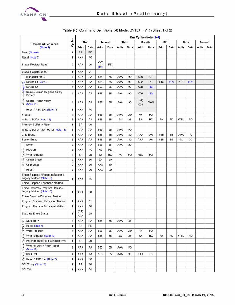
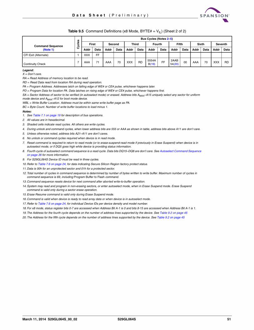
9. Command DefinitionsWriting specific address and data commands or sequences into the command register initiates device operations. Table 9.3 on page 46 and Table 9.5 on page 50 define the valid register command sequences. Writing incorrect address and data values or writing them in the improper sequence may place the device in an unknown state. A reset command is then required to return the device to reading array data.
All addresses are latched on the falling edge of WE# or CE#, whichever happens later. All data is latched on the rising edge of WE# or CE#, whichever happens first. Refer to AC Characteristics on page 87 for timing diagrams.
9.1 Reading Array DataThe device is automatically set to reading array data after device power-up. No commands are required to retrieve data. The device is ready to read array data after completing an Embedded Program or Embedded Erase algorithm.
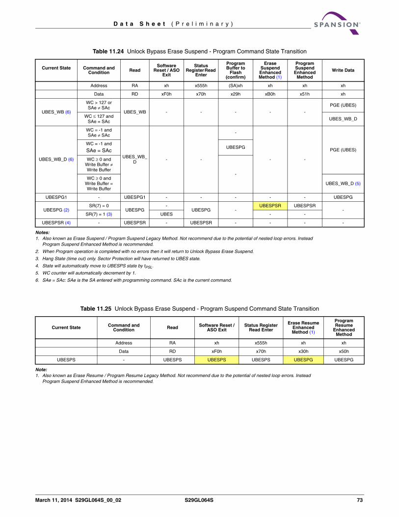
After the device accepts an Erase Suspend command, the device enters the erase-suspend-read mode, after which the system can read data from any non-erase-suspended sector. After completing a programming operation in the Erase Suspend mode, the system may once again read array data with the same exception. See Erase Suspend / Erase Resume Commands on page 43 for more information.
The system must issue the reset command to return the device to the read (or erase-suspend-read) mode if DQ5 goes high during an active program or erase operation, or if the device is in the autoselect mode. See Reset Command below for more information.
See also Requirements for Reading Array Data on page 20 for more information. The Read-Only Operations–AC Characteristics on page 87 provide the read parameters, and Figure 15.1 on page 89 shows the timing diagram.
9.2 Reset CommandWriting the reset command resets the device to the read or erase-suspend-read mode. Address bits are don’t cares for this command.
The reset command may be written between the sequence cycles in an erase command sequence before erasing begins. This resets the device to the read mode. Once erasure begins, however, the device ignores reset commands until the operation is complete.
The reset command may be written between the sequence cycles in a program command sequence before programming begins. This resets the device to the read mode. If the program command sequence is written while the device is in the Erase Suspend mode, writing the reset command returns the device to the erase-suspend-read mode. Once programming begins, however, the device ignores reset commands until the operation is complete.
The reset command may be written between the sequence cycles in an autoselect command sequence. Once in the autoselect mode, the reset command must be written to return to the read mode. If the device entered the autoselect mode while in the Erase Suspend mode, writing the reset command returns the device to the erase-suspend-read mode.
If DQ5 goes high during a program or erase operation, writing the reset command returns the device to the read mode (or erase-suspend-read mode if the device was in Erase Suspend).
Note that if DQ1 goes high during a Write Buffer Programming operation, the system must write the Write-to-Buffer-Abort Reset command sequence to reset the device for the next operation.
36 S29GL064S S29GL064S_00_02 March 11, 2014
D a t a S h e e t ( P r e l i m i n a r y )
9.3 Autoselect Command SequenceThe autoselect command sequence allows the host system to read several identifier codes at specific addresses:
Note:The device ID is read over three cycles. SA = Sector Address.
The autoselect command sequence is initiated by first writing on unlock cycle (two cycles). This is followed by a third write cycle that contains the autoselect command. The device then enters the autoselect mode. The system may read at any address any number of times without initiating another autoselect command sequence:
The system must write the reset command to return to the read mode (or erase-suspend-read mode if the device was previously in Erase Suspend).
9.4 Status Register ASOThe Status Register ASO contains a single word of registered volatile status for Embedded Algorithms. When the Status Register Read command is issued, the current status is captured by the register and the ASO is entered. The Status Register content appears at all word locations in the device address space. However, it is recommended to read the status only at word location 0 for future compatibility. The first read access in the Status Register ASO or a Software Reset / ASO Exit write command exits the ASO and returns to the address space map in use when the Status Register read command was issued. It is not recommended to perform any other command after the Status Register Read command is given and before the Status Register ASO is exited.
9.5 Enter / Exit Secure Silicon Region Command SequenceThe Secure Silicon Region provides a secured data area containing an 8-word / 16-byte random Electronic Serial Number (ESN). The system can access the Secure Silicon Region by issuing the three-cycle Enter Secure Silicon Region command sequence. The device continues to access the Secure Silicon Region until the system issues the four-cycle Exit Secure Silicon Region command sequence or Reset / ASO Exit command which returns the device to normal operation. Table 9.3 on page 46 and Table 9.5 on page 50 show the address and data requirements for both command sequences. See also Secure Silicon Region Flash Memory on page 29 for further information. Note that the ACC function and unlock bypass modes are not available when the Secure Silicon Region is enabled.
9.6 Word Program Command SequenceProgramming is a four-bus-cycle operation. The program command sequence is initiated by writing two unlock write cycles, followed by the program set-up command. The program address and data are written next, which in turn initiate the Embedded Program algorithm. The system is not required to provide further controls or timings. The device automatically provides internally generated program pulses and verifies the programmed cell margin. Table 9.3 on page 46 and Table 9.5 on page 50 show the address and data requirements for the word program command sequence, respectively.
When the Embedded Program algorithm is complete, the device then returns to the read mode and addresses are no longer latched. The system can determine the status of the program operation by using DQ7 or DQ6. Refer to Write Operation Status on page 55 for information on these status bits. Any commands written to the device during the Embedded Program Algorithm are ignored. Note that the Secure Silicon
Identifier CodeA7:A0(x16)
A6:A-1(x8)
Manufacturer ID 00h 00h
Device ID, Cycle 1 01h 02h
Device ID, Cycle 2 0Eh 1Ch
Device ID, Cycle 3 0Fh 1Eh
Secure Silicon Region Factory Protect 03h 06h
Sector Protect Verify (SA)02h (SA)04h
March 11, 2014 S29GL064S_00_02 S29GL064S 37
D a t a S h e e t ( P r e l i m i n a r y )
Region, autoselect, and CFI functions are unavailable when a program operation is in progress. Note that a hardware reset immediately terminates the program operation. The program command sequence should be reinitiated once the device returns to the read mode, to ensure data integrity.
Programming is allowed in any sequence of address locations and across sector boundaries. Programming to the same word address multiple times without intervening erases (incremental bit programming) requires a modified programming method. For such application requirements, please contact your local Spansion representative. Word programming is supported for backward compatibility with existing flash driver software and for occasional writing of individual words. Use of write buffer programming (see below) is strongly recommended for general programming use when more than a few words are to be programmed.
Any bit in a word cannot be programmed from 0 back to a 1. Attempting to do so may cause DQ7 and DQ6 status bits to indicate the operation was successful. However, a succeeding read shows that the data is still 0. Only erase operations can convert a 0 to a 1.
9.7 Unlock Bypass Command SequenceThis device features an Unlock Bypass mode to facilitate shorter programming and erase commands. Once the device enters the Unlock Bypass mode, only two write cycles are required to program or erase data, instead of the normal four or six cycles, respectively.
The unlock bypass command sequence is initiated by first writing two unlock cycles. This is followed by a third write cycle containing the unlock bypass command, 20h. The device then enters the unlock bypass mode.
This mode dispenses with the initial two unlock cycles required in the standard program sequence and four unlock cycles in the standard erase command sequence, resulting in faster total programming and erase times.Table 9.3 on page 46 and Table 9.5 on page 50 show the requirements for the unlock bypass command sequences.
During the unlock bypass mode, only the Read, Program, Write Buffer Programming, Write-to-Buffer-Abort Reset, Unlock Bypass Sector Erase, Unlock Bypass Chip Erase and Unlock Bypass Reset commands are valid. To exit the unlock bypass mode, the system must issue the two-cycle unlock bypass reset command sequence. The first cycle address is ‘don't care’ and the data 90h. The second cycle need only contain the data 00h. The sector then returns to the read mode.
9.8 Write Buffer ProgrammingWrite Buffer Programming allows the system write to a maximum of 128 words / 256 bytes in one programming operation. This results in faster effective programming time than the standard programming algorithms. The Write Buffer Programming command sequence is initiated by first writing two unlock cycles. This is followed by a third write cycle containing the Write Buffer Load command written at the Sector Address in which programming occurs. The fourth cycle writes the sector address and the number of word locations, minus one, to be programmed. For example, if the system programs six unique address locations, then 05h should be written to the device. This tells the device how many write buffer addresses are loaded with data and therefore when to expect the Program Buffer to Flash command. The number of locations to program cannot exceed the size of the write buffer or the operation aborts.
The fifth cycle writes the first address location and data to be programmed. The write-buffer-page is selected by address bits AMAX–A7. All subsequent address / data pairs must fall within the selected-write-buffer-page. The system then writes the remaining address / data pairs into the write buffer. Write buffer locations may be loaded in any order.
The write-buffer-page address must be the same for all address / data pairs loaded into the write buffer. (This means Write Buffer Programming cannot be performed across multiple write-buffer pages.) This also means that Write Buffer Programming cannot be performed across multiple sectors. If the system attempts to load programming data outside of the selected write-buffer page, the operation aborts.
Note that if a Write Buffer address location is loaded multiple times, the address / data pair counter is decremented for every data load operation. The host system must therefore account for loading a write-buffer location more than once. The counter decrements for each data load operation, not for each unique write-buffer-address location. Note also that if an address location is loaded more than once into the buffer, the final data loaded for that address is programmed.
38 S29GL064S S29GL064S_00_02 March 11, 2014
D a t a S h e e t ( P r e l i m i n a r y )
Once the specified number of write buffer locations are loaded, the system must then write the Program Buffer to Flash command at the sector address. Any other address and data combination aborts the Write Buffer Programming operation. The device then begins programming. Data polling should be used while monitoring the last address location loaded into the write buffer. DQ7, DQ6, DQ5, and DQ1 should be monitored to determine the device status during Write Buffer Programming.
The write-buffer programming operation can be suspended using the standard program suspend / resume commands. Upon successful completion of the Write Buffer Programming operation, the device is ready to execute the next command.
The Write Buffer Programming Sequence can be aborted in the following ways:
Load a value that is greater than the page buffer size during the Number of Locations to Program step.
Write to an address in a sector different than the one specified during the Write-Buffer-Load command.
Write an Address / Data pair to a different write-buffer-page than the one selected by the Starting Address during the write buffer data loading stage of the operation.
Write data other than the Confirm Command after the specified number of data load cycles.
The abort condition is indicated by DQ1 = 1, DQ7 = DATA# (for the last address location loaded), DQ6 = toggle, and DQ5 = 0. A Write-to-Buffer-Abort Reset command sequence must be written to reset the device for the next operation.
Note that the Secure Silicon Region, autoselect, and CFI functions are unavailable when a program operation is in progress. This flash device is capable of handling multiple write buffer programming operations on the same write buffer address range without intervening erases. For applications requiring incremental bit programming, a modified programming method is required; please contact your local Spansion representative. Any bit in a write buffer address range cannot be programmed from 0 back to a 1. Attempting to do so may cause the device to set DQ5 = 1, of cause the DQ7 and DQ6 status bits to indicate the operation was successful. However, a succeeding read shows that the data is still 0. Only erase operations can convert a 0 to a 1.
9.9 Accelerated ProgramThe device supports program operations when the system asserts VHH on the WP#/ACC or ACC pin. When WP#/ACC or ACC pin is lowered back to VIH or VIL the device exits the Accelerated Programming mode and returns to normal operation. The WP#/ACC is VHH tolerant but is not designed to accelerate the program functions. If the system asserts VHH on this input, the device automatically enters the Unlock Bypass mode. The system can then use the Write Buffer Load command sequence provided by the Unlock Bypass mode. Note that if a Write-to-Buffer-Abort Reset is required while in Unlock Bypass mode, the full 3-cycle RESET command sequence must be used to reset the device. Note that the WP#/ACC pin must not be at VHH for operations other than accelerated programming, or device damage may result. WP# contains an internal pull-up; when unconnected, WP# is at VIH. Accelerated programming is supported at room temperature only.
Figure 9.1 on page 39 illustrates the algorithm for the program operation. Refer to Table 15.4, Erase / Program Operations on page 93 for parameters, and Figure 15.12 on page 94 for timing diagrams.
Sectors must be unlocked prior to raising WP#/ACC to VHH.
It is recommended that WP#/ACC apply VHH after power-up sequence is completed. In addition, it is recommended that WP#/ACC apply from VHH to VIH/VIL before powering down VCC/VIO.
March 11, 2014 S29GL064S_00_02 S29GL064S 39
D a t a S h e e t ( P r e l i m i n a r y )
Figure 9.1 Write Buffer Programming Operation
Notes:1. When Sector Address is specified, any address in the selected sector is acceptable. However, when loading Write-Buffer address
locations with data, all addresses must fall within the selected Write-Buffer Page.
2. DQ7 may change simultaneously with DQ5. Therefore, DQ7 should be verified.
3. If this flowchart location was reached because DQ5= 1, then the device Failed. If this flowchart location was reached because DQ1= 1, then the Write to Buffer operation was Aborted. In either case, the proper reset command must be written before the device can begin another operation. If DQ1= 1, write the Write-Buffer-Programming-Abort-Reset command. if DQ5= 1, write the Reset command.
4. See Table 9.3 on page 46 and Table 9.5 on page 50 for command sequences required for write buffer programming.
Write “Write to Buffer” command and Sector Address
Write number of addressesto program minus 1(WC)
and Sector Address
Write program buffer toflash sector address
Write first address/data
Write to a differentsector address
FAIL or ABORT PASS
Read DQ7 - DQ0 atLast Loaded Address
Read DQ7 - DQ0 with address = Last Loaded
Address
Write next address/data pair
WC = WC - 1
WC = 0 ?
Part of “Write to Buffer”Command Sequence
Yes
Yes
Yes
Yes
YesYes
No
No
No
No
No
No
Abort Write toBuffer Operation?
DQ7 = Data?
DQ7 = Data?
DQ5 = 1?DQ1 = 1?
Write to buffer ABORTED.Must write “Write-to-buffer
Abort Reset” commandsequence to return
to read mode.
(Note 2)
(Note 3)
(Note 1)
40 S29GL064S S29GL064S_00_02 March 11, 2014
D a t a S h e e t ( P r e l i m i n a r y )
Figure 9.2 Program Operation
Note:See Table 9.3 on page 46 and Table 9.5 on page 50 for program command sequence.
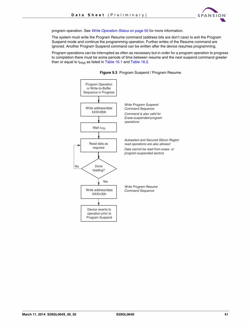
9.10 Program Suspend / Program Resume Command SequenceThe Program Suspend command allows the system to interrupt a programming operation or a Write to Buffer programming operation so that data can be read from any non-suspended sector. When the Program Suspend command is written during a programming process, the device halts the program operation within tPSL (program suspend latency) and updates the status bits. Addresses are not required when writing the Program Suspend command.
There are two commands available for program suspend. The legacy combined Erase / Program suspend command (B0h command code) and the separate Program Suspend command (51h command code). There are also two commands for Program resume. The legacy combined Erase / Program resume command (30h command code) and the separate Program Resume command (50h command code). It is recommended to use the separate program suspend and resume commands for programming and use the legacy combined command only for erase suspend and resume.
After the programming operation is suspended, the system can read array data from any non-suspended sector. The Program Suspend command may also be issued during a programming operation while an erase is suspended. In this case, data may be read from any addresses not in Erase Suspend or Program Suspend. If a read is needed from the Secure Silicon Region area (One-time Program area), then user must use the proper command sequences to enter and exit this region. Note that the Secure Silicon Region, autoselect, and CFI functions are unavailable when a program operation is in progress.
The system may also write the autoselect command sequence when the device is in the Program Suspend mode. The system can read as many autoselect codes as required. When the device exits the autoselect mode, the device reverts to the Program Suspend mode, and is ready for another valid operation. See Autoselect Command Sequence on page 36 for more information.
After the Program Resume command is written, the device reverts to programming. The system can determine the status of the program operation using the DQ7 or DQ6 status bits, just as in the standard
START
Write ProgramCommand Sequence
Data Poll from System
Verify Data?No
Yes
Last Address?No
Yes
Programming Completed
Increment Address
Embedded Program
algorithm in progress
March 11, 2014 S29GL064S_00_02 S29GL064S 41
D a t a S h e e t ( P r e l i m i n a r y )
program operation. See Write Operation Status on page 55 for more information.
The system must write the Program Resume command (address bits are don’t care) to exit the Program Suspend mode and continue the programming operation. Further writes of the Resume command are ignored. Another Program Suspend command can be written after the device resumes programming.
Program operations can be interrupted as often as necessary but in order for a program operation to progress to completion there must be some periods of time between resume and the next suspend command greater than or equal to tPRS as listed in Table 16.1 and Table 16.2.
Figure 9.3 Program Suspend / Program Resume
Program Operationor Write-to-Buffer
Sequence in Progress
Write Program SuspendCommand Sequence
Command is also valid for Erase-suspended-programoperations
Autoselect and Secured Silicon Regionread operations are also allowed
Data cannot be read from erase- orprogram-suspended sectors
9.11 Chip Erase Command SequenceChip erase is a six bus cycle operation. The chip erase command sequence is initiated by writing two unlock cycles, followed by a set-up command. Two additional unlock write cycles are then followed by the chip erase command, which in turn invokes the Embedded Erase algorithm. The device does not require the system to pre-program prior to erase. The Embedded Erase algorithm automatically preprograms and verifies the entire memory for an all zero data pattern prior to electrical erase. The system is not required to provide any controls or timings during these operations. Table 9.3 on page 46 and Table 9.5 on page 50 show the address and data requirements for the chip erase command sequence.
When the Embedded Erase algorithm is complete, the device returns to the read mode and addresses are no longer latched. The system can determine the status of the erase operation by using DQ7, DQ6, or DQ2. Refer to Write Operation Status on page 55 for information on these status bits.
The Unlock Bypass feature allows the host system to send program commands to the flash device without first writing unlock cycles within the command sequence. See Section 9.7 for details on the Unlock Bypass function.
Any commands written during the chip erase operation are ignored. However, note that a hardware reset immediately terminates the erase operation. If this occurs, the chip erase command sequence should be reinitiated once the device returns to reading array data, to ensure data integrity.
Figure 9.4 on page 43 illustrates the algorithm for the erase operation. Refer to Table 15.2 on page 90 for parameters, and Figure 15.13 on page 95 for timing diagrams.
9.12 Sector Erase Command SequenceSector erase is a six bus cycle operation. The sector erase command sequence is initiated by writing two unlock cycles, followed by a set-up command. Two additional unlock cycles are written, and are then followed by the address of the sector to be erased, and the sector erase command. Table 9.3 on page 46 and Table 9.5 on page 50 shows the address and data requirements for the sector erase command sequence.
The device does not require the system to pre-program prior to erase. The Embedded Erase algorithm automatically programs and verifies the entire memory for an all zero data pattern prior to electrical erase. The system is not required to provide any controls or timings during these operations.
After the command sequence is written, a sector erase time-out of tSEA occurs. During the time-out period, additional sector addresses and sector erase commands may be written. Invalid commands will be ignored during the time-out period. Loading the sector erase buffer may be done in any sequence, and the number of sectors may be from one sector to all sectors. The time between these additional cycles must be less than 50 µs, otherwise erasure may begin. Any sector erase address and command following the exceeded time-out may or may not be accepted. It is recommended that processor interrupts be disabled during this time to ensure all commands are accepted. The interrupts can be re-enabled after the last Sector Erase command is written. Note that the Secure Silicon Region, autoselect, and CFI functions are unavailable when an erase operation is in progress. The system must rewrite the command sequence and any additional addresses and commands.
The system can monitor DQ3 to determine if the sector erase timer has timed out (See DQ3: Sector Erase Timer on page 59.). The time-out begins from the rising edge of the final WE# pulse in the command sequence.
If the sector is found to have not completed its last erase successfully, the sector is unconditionally erased. If the last erase was successful, the sector is read to determine if the sector is still erased (blank). The erase operation is started immediately after finding any programmed zero. If the sector is already blank (no programmed zero bit found) the remainder of the erase operation is skipped. This can dramatically reduce erase time when sectors being erased do not need the erase operation. When enabled the blank check feature is used within the parameter erase, sector erase, and bulk erase commands. When blank check is disabled an erase command unconditionally starts the erase operation.
When the Embedded Erase algorithm is complete, the device returns to reading array data and addresses are no longer latched. The system can determine the status of the erase operation by reading DQ7, DQ6, or DQ2 in the erasing sector. Refer to Write Operation Status on page 55 for information on these status bits.
March 11, 2014 S29GL064S_00_02 S29GL064S 43
D a t a S h e e t ( P r e l i m i n a r y )
Once the sector erase operation begins, only the Erase Suspend command is valid. All other commands are ignored. However, note that a hardware reset immediately terminates the erase operation. If that occurs, the sector erase command sequence should be reinitiated once the device returns to reading array data, to ensure data integrity.
Figure 9.4 on page 43 illustrates the algorithm for the erase operation. Refer to Table 15.2 on page 90 for parameters, and Figure 15.13 on page 95 for timing diagrams.
Figure 9.4 Erase Operation
Notes:1. See Table 9.3 and Table 9.5 for program command sequence.
2. See DQ3: Sector Erase Timer on page 59 for information on the sector erase timer.
9.13 Erase Suspend / Erase Resume CommandsThe Erase Suspend command, B0h, allows the system to interrupt a sector erase operation and then read data from, or program data to, any sector not selected for erasure. This command is valid only during the sector erase operation, including the tESL time-out period during the sector erase command sequence. The Erase Suspend command is ignored if written during the chip erase operation or Embedded Program algorithm.
When the Erase Suspend command is written during the sector erase operation, the device requires tESL (erase suspend latency) to suspend the erase operation. However, when the Erase Suspend command is written during the sector erase time-out, the device immediately terminates the time-out period and suspends the erase operation.
After the erase operation is suspended, the device enters the erase-suspend-read mode. The system can read data from or program data to any sector not selected for erasure. (The device erase suspends all sectors selected for erasure.) Reading at any address within erase-suspended sectors produces status information on DQ7–DQ0. The system can use DQ7, or DQ6 and DQ2 together, to determine if a sector is actively erasing or is erase-suspended. Refer to Write Operation Status on page 55 for information on these status bits.
After an erase-suspended program operation is complete, the device returns to the erase-suspend-read mode. The system can determine the status of the program operation using the DQ7 or DQ6 status bits, just as in the standard word program operation. Refer to Write Operation Status on page 55 for more information.
START
Write Erase Command Sequence
(Notes 1, 2)
Data Poll to Erasing Bank from System
Data = FFh?No
Yes
Erasure Completed
Embedded Erasealgorithmin progress
44 S29GL064S S29GL064S_00_02 March 11, 2014
D a t a S h e e t ( P r e l i m i n a r y )
In the erase-suspend-read mode, the system can also issue the autoselect command sequence. Refer to the Autoselect Mode on page 24 and Autoselect Command Sequence on page 36 sections for details.
To resume the sector erase operation, the system must write the Erase Resume command. Further writes of the Resume command are ignored. Another Erase Suspend command can be written after the chip resumes erasing.
During an erase operation, this flash device performs multiple internal operations which are invisible to the system. When an erase operation is suspended, any of the internal operations that were not fully completed must be restarted. As such, if this flash device is continually issued suspend / resume commands in rapid succession, erase progress is impeded as a function of the number of suspends. The result is a longer cumulative erase time than without suspends. Note that the additional suspends do not affect device reliability or future performance. In most systems rapid erase / suspend activity occurs only briefly. In such cases, erase performance is not significantly impacted.
Erase operations can be interrupted as often as necessary but in order for an erase operation to progress to completion there must be some periods of time between resume and the next suspend command greater than or equal to tERS as listed in Table 16.1 and Table 16.2.
9.14 Evaluate Erase StatusThe Evaluate Erase Status (EES) command verifies that the last erase operation on the addressed sector was completed successfully. The EES command can be used to detect erase operations failed due to loss of power, reset, or failure during the erase operation.
To initiate a EES on a Sector, write 35h to the sector address (SA), while the EAC is in the standby state
The ESS command may not be written while the device is actively programming or erasing or suspended.
The EES command does not allow for reads to the array during the operation. Reads to the array while this command is executing will return unknown data.
Use the Status Register read to confirm if the device is still busy and when complete if the sector is erased or not. Bit 7 of the Status Register will show if the device is performing a ESS (similar to an erase operation). Bit 5 of the Status Register will be cleared to 0 if the sector is erased and set to 1 if not erased.
As soon as any bit is found to not be erased, the device will halt the operation and report the results.
Once the ESS is completed, the EAC will return to the Standby State.
The EES command requires tEES (refer to Table 16.1 on page 99) to complete and update the erase status in SR. The DRB bit (SR[7]) may be read to determine when the EES command is finished. If a sector is found not erased with SR[5]=1, the sector must be erased again to ensure reliable storage of data in the sector.
9.15 Continuity CheckThe Continuity Check provides a basic test of connectivity from package connectors to each die pad. This feature is an extension of the legacy unlock cycle sequence used at the beginning of several commands. The unlock sequence is two writes with alternating ones and zeros pattern on the lower portion of the address and data lines with the pattern inverted between the first and second write.
To perform a continuity check these patterns are extended to cover all address and data lines:
A logic comparison circuit looks for the alternating one and zero pattern that is inverted between the two write cycles.
When the correct patterns are detected, the status register bit zero is set to 1. The status register clear command will clear the status register bit zero to a 0.
Address Bus Data Bus
x16 Mode AMAX - A0 D15-D0
x8 Mode AMAX - A-1 D7-D0
March 11, 2014 S29GL064S_00_02 S29GL064S 45
D a t a S h e e t ( P r e l i m i n a r y )
The alternating one and zero pattern checks for adjacent wire shorts. The inversion of the pattern between cycles checks for stuck-at faults. The status output being cleared and set checks for stuck-at faults on the status output. Checking for different status results from each die checks for working die selection logic.
Table 9.1 x16 Data Bus
PhaseAccess
Type
S29GL064S
Data CommentAddress A21 to A0
Set-Up
Write 555 XX71 Clear die status
Write 555 XX70 Write Status Register Read command to die
Read XXX RD Read status from die to confirm status bit zero = 0
Continuity PatternWrite 2AAA55 FF00 First continuity cycle
Write 1555AA 00FF Second continuity cycle
Verify continuity pattern detected
Write 555 XX70 Write Status Register Read command to die
Read XXX RDRead status from die to confirm status bit zero = 1 for continuity pattern detected
Table 9.2 X8 Data Bus
PhaseAccess
Type
S29GL064S
Data CommentAddress A21 to A-1
Set-Up
Write AAA 71 Clear die status
Write AAA 70 Write Status Register Read command to die
Read XXX RD Read status from die to confirm status bit zero = 0
Continuity PatternWrite 5554AB FF First continuity cycle
Write 2AAB54 00 Second continuity cycle
Verify continuity pattern detected
Write AAA 70 Write Status Register Read command to die
Read XXX RDRead status from die to confirm status bit zero = 1 for continuity pattern detected
Legend:X = Don’t care.RA = Read Address of memory location to be read. RD = Read Data read from location RA during read operation.PA = Program Address. Addresses latch on falling edge of WE# or CE# pulse, whichever happens later.PD = Program Data for location PA. Data latches on rising edge of WE# or CE# pulse, whichever happens first.SA = Sector Address of sector to be verified (in autoselect mode) or erased. Address bits AMAX–A15 uniquely select any sector for uniform mode device and AMAX–A12 for boot mode device.WBL = Write Buffer Location. Address must be within same write buffer page as PA.WC = Word Count. Number of write buffer locations to load minus 1.
Notes:1. See Table 7.1 on page 19 for description of bus operations.
2. All values are in hexadecimal.
3. Shaded cells indicate read cycles. All others are write cycles.
4. During unlock and command cycles, when lower address bits are 555 or 2AA as shown in table, address bits above A11 and data bits above DQ7 are don’t care.
5. No unlock or command cycles required when device is in read mode.
6. Reset command is required to return to read mode (or to erase-suspend-read mode if previously in Erase Suspend) when device is in autoselect mode, or if DQ5 goes high while device is providing status information.
7. Fourth cycle of the autoselect command sequence is a read cycle. Data bits DQ15–DQ8 are don’t care. Except for RD, PD and WC. See Autoselect Command Sequence on page 36 for more information.
8. Device ID must be read in three cycles.
9. Refer to Table 7.6 on page 24 for data indicating Secure Silicon Region factory protect status.
10. Data is 00h for an unprotected sector and 01h for a protected sector.
11. Total number of cycles in command sequence is determined by number of words written to write buffer. Maximum number of cycles in command sequence is 37, including Program Buffer to Flash command.
12. Command sequence resets device for next command after aborted write-to-buffer operation.
13. Unlock Bypass command is required prior to Unlock Bypass Program command.
14. Unlock Bypass Reset command is required to return to read mode when device is in unlock bypass mode.
15. System may read and program in non-erasing sectors, or enter autoselect mode, when in Erase Suspend mode. Erase Suspend command is valid only during a sector erase operation.
16. Erase Resume command is valid only during Erase Suspend mode.
17. Command is valid when device is ready to read array data or when device is in autoselect mode.
18. Refer to Table 7.6 on page 24, for individual Device IDs per device density and model number.
19. The Address for the fourth cycle depends on the number of address lines supported by the device. See Table 9.1 on page 45.
20. The Address for the fifth cycle depends on the number of address lines supported by the device. See Table 9.1 on page 45.
Addr Data Addr Data Addr Data Addr Data Addr Data Addr Data Addr Data
48 S29GL064S S29GL064S_00_02 March 11, 2014
D a t a S h e e t ( P r e l i m i n a r y )
Legend:X = Don’t care.RA = Address of the memory location to be read. SA = Sector Address. Any address that falls within a specified sector. See Tables 7.2 – 7.5 for sector address ranges.PWAx = PPB Password address for word0 = 00h, word1 = 01h, word2 = 02h, and word3 = 03h (Sector Address = Word Line = 0).PWDx = Password data word0, word1, word2, and word3. RD(0) = DQ0 protection indicator bit. If protected, DQ0 = 0. If unprotected, DQ0 = 1.Gray vs. White Box = Read vs. Write Operation.
Notes:1. All values are in hexadecimal.
2. Shaded cells indicate read cycles. All others are write cycles.
3. Address and data bits not specified in table, legend, or notes are don’t cares (each hex digit implies 4 bits of data).
4. Writing incorrect address and data values or writing them in the improper sequence may place the device in an unknown state. The system must write the reset command to return the device to reading array data.
Table 9.4 Sector Protection Commands (x16)
Command Sequence(Notes) C
ycle
s Bus Cycles (Notes 2–4)
First Second Third Fourth Fifth Sixth Seventh
Addr Data Addr Data Addr Data Addr Data Addr Data Addr Data Addr Data
Write to Buffer (Note 12) 6 AAA AA 555 55 SA 25 SA BC PA PD WBL PD
Program Buffer to Flash (confirm) 1 SA 29
Write-to-Buffer-Abort Reset (Note 13)
3 AAA AA 555 55 AAA F0
SSR Exit 4 AAA AA 555 55 AAA 90 XXX 00
Reset / ASO Exit (Note 7) 1 XXX F0
CFI Query (Note 16) 1 AA 98
CFI Exit 1 XXX F0
March 11, 2014 S29GL064S_00_02 S29GL064S 51
D a t a S h e e t ( P r e l i m i n a r y )
Legend:X = Don’t care.RA = Read Address of memory location to be read. RD = Read Data read from location RA during read operation.PA = Program Address. Addresses latch on falling edge of WE# or CE# pulse, whichever happens later.PD = Program Data for location PA. Data latches on rising edge of WE# or CE# pulse, whichever happens first.SA = Sector Address of sector to be verified (in autoselect mode) or erased. Address bits AMAX–A15 uniquely select any sector for uniform mode device and AMAX–A12 for boot mode device.WBL = Write Buffer Location. Address must be within same write buffer page as PA.BC = Byte Count. Number of write buffer locations to load minus 1.
Notes:1. See Table 7.1 on page 19 for description of bus operations.
2. All values are in hexadecimal.
3. Shaded cells indicate read cycles. All others are write cycles.
4. During unlock and command cycles, when lower address bits are 555 or AAA as shown in table, address bits above A11 are don’t care.
5. Unless otherwise noted, address bits A21–A11 are don’t cares.
6. No unlock or command cycles required when device is in read mode.
7. Reset command is required to return to read mode (or to erase-suspend-read mode if previously in Erase Suspend) when device is in autoselect mode, or if DQ5 goes high while device is providing status information.
8. Fourth cycle of autoselect command sequence is a read cycle. Data bits DQ15–DQ8 are don’t care. See Autoselect Command Sequence on page 36 for more information.
9. For S29GL064S Device ID must be read in three cycles.
10. Refer to Table 7.6 on page 24, for data indicating Secure Silicon Region factory protect status.
11. Data is 00h for an unprotected sector and 01h for a protected sector.
12. Total number of cycles in command sequence is determined by number of bytes written to write buffer. Maximum number of cycles in command sequence is 69, including Program Buffer to Flash command.
13. Command sequence resets device for next command after aborted write-to-buffer operation.
14. System may read and program in non-erasing sectors, or enter autoselect mode, when in Erase Suspend mode. Erase Suspend command is valid only during a sector erase operation.
15. Erase Resume command is valid only during Erase Suspend mode.
16. Command is valid when device is ready to read array data or when device is in autoselect mode.
17. Refer to Table 7.6 on page 24, for individual Device IDs per device density and model number.
18. For x8 mode, status register bits 0-7 are accessed when Address Bit A-1 is 0 and bits 8-15 are accessed when Address Bit A-1 is 1.
19. The Address for the fourth cycle depends on the number of address lines supported by the device. See Table 9.2 on page 45
20. The Address for the fifth cycle depends on the number of address lines supported by the device. See Table 9.2 on page 45
Addr Data Addr Data Addr Data Addr Data Addr Data Addr Data Addr Data
52 S29GL064S S29GL064S_00_02 March 11, 2014
D a t a S h e e t ( P r e l i m i n a r y )
Legend:X = Don’t care.RA = Address of the memory location to be read. SA = Sector Address. Any address that falls within a specified sector. See Tables 7.2 – 7.5 for sector address ranges.PWAx = PPB Password address for byte0 = 00h, byte1 = 01h, byte2 = 02h, byte3 = 03h, byte04= 04h, byte5 = 05h, byte6 = 06h, and byte7 = 07h (Sector Address = Word Line = 0).PWDx = Password data byte0, byte1, byte2, byte3, byte4, byte5, byte6, and byte7.RD(0) = DQ0 protection indicator bit. If protected, DQ0 = 0. If unprotected, DQ0 = 1.Gray vs. White Box = Read vs. Write Operation.
Notes:1. All values are in hexadecimal.
2. Shaded cells indicate read cycles. All others are write cycles.
3. Address and data bits not specified in table, legend, or notes are don’t cares (each hex digit implies 4 bits of data).
4. Writing incorrect address and data values or writing them in the improper sequence may place the device in an unknown state. The system must write the reset command to return the device to reading array data.
5. Entry commands are required to enter a specific mode to enable instructions only available within that mode.
Table 9.6 Sector Protection Commands (x8)
Command Sequence(Notes) C
ycle
s Bus Cycles (Notes 2–5)
1st/8th 2nd/9th 3rd/10th 4th/11th 5th 6th 7th
Addr Data Addr Data Addr Data Addr Data Addr Data Addr Data Addr Data
6. No unlock or command cycles required when bank is reading array data.
7. Exit command must be issued to reset the device into read mode; device may otherwise be placed in an unknown state.
8. Entire two bus-cycle sequence must be entered for each portion of the password.
9. Full address range is required for reading password.
10. Password may be unlocked or read in any order. Unlocking requires the full password (all seven cycles).
11. ACC must be at VIH when setting PPB or DYB.
12. “All PPB Erase” command pre-programs all PPBs before erasure to prevent over-erasure.
54 S29GL064S S29GL064S_00_02 March 11, 2014
D a t a S h e e t ( P r e l i m i n a r y )
10. Status MonitoringThere are three methods for monitoring EA status. Previous generations of the S29GL flash family used the methods called Data Polling and Ready/Busy# (RY/BY#) Signal. These methods are still supported by the S29GL-S family. One additional method is reading the Status Register.
10.1 Status RegisterThe status of program and erase operations is provided by a single 16-bit status register. The Status Register Read command is written followed by one read access of the status register information. The contents of the status register is aliased (overlaid) in all locations of the device address space. The overlay is in effect for one read access, specifically the next read access that follows the Status Register Read command. After the one status register access, the Status Register ASO is exited. The CE# or OE# signal must go High following the status register read access for tCEPH/tOEPH time to return to the address space active at the time the Status Register Read command was issued.
The status register contains bits related to the results - success or failure - of the most recently completed Embedded Algorithms (EA):
Erase Status (bit 5),
Program Status (bit 4),
Write Buffer Abort (bit 3),
Sector Locked Status (bit 1),
RFU (bit 0).
and, bits related to the current state of any in process EA:
Device Busy (bit 7),
Erase Suspended (bit 6),
Program Suspended (bit 2),
The current state bits indicate whether an EA is in process, suspended, or completed.
The upper 8 bits (bits 15:8) are reserved. These have undefined High or Low value that can change from one status read to another. These bits should be treated as don't care and ignored by any software reading status.
The Clear Status Register Command will clear to 0 the results related bits of the status register but will not affect the current state bits.
Initiation of an embedded operation will first clear the status register bits.
March 11, 2014 S29GL064S_00_02 S29GL064S 55
D a t a S h e e t ( P r e l i m i n a r y )
Notes:1. Bits 15 thru 8, and 0 are reserved for future use and may display as 0 or 1. These bits should be ignored (masked) when checking status.
2. Bit 7 is 1 when there is no Embedded Algorithm in progress in the device.
3. Bits 6 thru 1 are valid only if Bit 7 is 1.
4. All bits are put in their reset status by cold reset or warm reset.
5. Bits 5, 4, 3, and 1 and 0 are cleared to 0 by the Clear Status Register command or Reset command.
6. Upon issuing the Erase Suspend Command, the user must continue to read status until DRB becomes 1.
7. ESSB is cleared to 0 by the Erase Resume Command.
8. ESB reflects success or failure of the most recent erase operation.
9. PSB reflects success or failure of the most recent program operation.
10. During erase suspend, programming to the suspended sector, will cause program failure and set the Program status bit to 1.
11. Upon issuing the Program Suspend Command, the user must continue to read status until DRB becomes 1.
12. PSSB is cleared to 0 by the Program Resume Command.
13. SLSB indicates that a program or erase operation failed because the sector was locked.
14. SLSB reflects the status of the most recent program or erase operation.
10.2 Write Operation StatusThe device provides several bits to determine the status of a program or erase operation: DQ2, DQ3, DQ5, DQ6, and DQ7. Table 10.2 on page 60 and the following subsections describe the function of these bits. DQ7 and DQ6 each offer a method for determining whether a program or erase operation is complete or in progress. The device also provides a hardware-based output signal, RY/BY#, to determine whether an Embedded Program or Erase operation is in progress or is completed.
10.3 DQ7: Data# PollingThe Data# Polling bit, DQ7, indicates to the host system whether an Embedded Program or Erase algorithm is in progress or completed, or whether the device is in Erase Suspend. Data# Polling is valid after the rising edge of the final WE# pulse in the command sequence.
During the Embedded Program algorithm, the device outputs on DQ7 the complement of the datum programmed to DQ7. This DQ7 status also applies to programming during Erase Suspend. When programming in x8 mode, the DQ7 polling value will be the DATA# of the last byte entered, regardless if the byte is at an even or odd address. When the Embedded Program algorithm is complete, the device outputs the datum programmed to DQ7. The system must provide the program address to read valid status information on DQ7. If a program address falls within a protected sector, Data# Polling on DQ7 is active for approximately tDP, then the device returns to the read mode.
During the Embedded Erase algorithm, Data# Polling produces a 0 on DQ7. When the Embedded Erase algorithm is complete, or if the device enters the Erase Suspend mode, Data# Polling produces a 1 on DQ7. The system must provide an address within any of the sectors selected for erasure to read valid status information on DQ7.
After an erase command sequence is written, if all sectors selected for erasing are protected, Data# Polling on DQ7 is active for approximately tDP, then the device returns to the read mode. If not all selected sectors are protected, the Embedded Erase algorithm erases the unprotected sectors, and ignores the selected sectors that are protected. However, if the system reads DQ7 at an address within a protected sector, the status may not be valid.
Just prior to the completion of an Embedded Program or Erase operation, DQ7 may change asynchronously with DQ0–DQ6 while Output Enable (OE#) is asserted low. That is, the device may change from providing status information to valid data on DQ7. Depending on when the system samples the DQ7 output, it may read the status or valid data. Even if the device completed the program or erase operation and DQ7 has valid data, the data outputs on DQ0–DQ6 may be still invalid. Valid data on DQ0–DQ7 appears on successive read cycles.
Table 10.2 on page 60 shows the outputs for Data# Polling on DQ7. Figure 10.1 on page 56 shows the Data# Polling algorithm. Figure 15.14 on page 95 shows the Data# Polling timing diagram.
Figure 10.1 Data# Polling Algorithm
Notes:1. VA = Valid address for programming. During a sector erase operation, a valid address is any sector address within the sector being
erased. During chip erase, a valid address is any non-protected sector address.
2. DQ7 should be rechecked even if DQ5 = 1 because DQ7 may change simultaneously with DQ5.
DQ7 = Data? Yes
No
No
DQ5 = 1?No
Yes
Yes
FAIL PASS
Read DQ15–DQ0Addr = VA
Read DQ15–DQ0Addr = VA
DQ7 = Data?
START
March 11, 2014 S29GL064S_00_02 S29GL064S 57
D a t a S h e e t ( P r e l i m i n a r y )
10.4 DQ6: Toggle Bit IToggle Bit I on DQ6 indicates whether an Embedded Program or Erase algorithm is in progress or complete, or whether the device entered the Erase Suspend mode. Toggle Bit I may be read at any address, and is valid after the rising edge of the final WE# pulse in the command sequence (prior to the program or erase operation), and during the sector erase time-out.
During an Embedded Program or Erase algorithm operation, successive read cycles to any address cause DQ6 to toggle. The system may use either OE# or CE# to control the read cycles. When the operation is complete, DQ6 stops toggling.
After an erase command sequence is written, if all sectors selected for erasing are protected, DQ6 toggles for approximately tDP, then returns to reading array data. If not all selected sectors are protected, the Embedded Erase algorithm erases the unprotected sectors, and ignores the selected sectors that are protected.
The system can use DQ6 and DQ2 together to determine whether a sector is actively erasing or is erase-suspended. When the device is actively erasing (that is, the Embedded Erase algorithm is in progress), DQ6 toggles. When the device enters the Erase Suspend mode, DQ6 stops toggling. However, the system must also use DQ2 to determine which sectors are erasing or erase-suspended. Alternatively, the system can use DQ7 (see DQ7: Data# Polling on page 55).
If a program address falls within a protected sector, DQ6 toggles for approximately tDP after the program command sequence is written, then returns to reading array data.
DQ6 also toggles during the erase-suspend-program mode, and stops toggling once the Embedded Program algorithm is complete.
Table 10.2 on page 60 shows the outputs for Toggle Bit I on DQ6. Figure 10.2 on page 58 shows the toggle bit algorithm. Figure 15.15 on page 96 shows the toggle bit timing diagrams. Figure 15.16 on page 96 shows the differences between DQ2 and DQ6 in graphical form. See also DQ2: Toggle Bit II on page 59.
58 S29GL064S S29GL064S_00_02 March 11, 2014
D a t a S h e e t ( P r e l i m i n a r y )
Figure 10.2 Toggle Bit Algorithm
Note:The system should recheck the toggle bit even if DQ5 = 1 because the toggle bit may stop toggling as DQ5 changes to 1. See Reading Toggle Bits DQ6/DQ2 on page 59 for more information.
START
No
Yes
Yes
DQ5 = 1?No
Yes
Toggle Bit = Toggle?
No
Program/EraseOperation Not
Complete, Write Reset Command
Program/EraseOperation Complete
Read DQ7–DQ0
Toggle Bit = Toggle?
Read DQ7–DQ0Twice
Read DQ7–DQ0
March 11, 2014 S29GL064S_00_02 S29GL064S 59
D a t a S h e e t ( P r e l i m i n a r y )
10.5 DQ2: Toggle Bit IIThe “Toggle Bit II” on DQ2, when used with DQ6, indicates whether a particular sector is actively erasing (that is, the Embedded Erase algorithm is in progress), or whether that sector is erase-suspended. (The Toggle Bit II does not apply to the PPB erase command.) Toggle Bit II is valid after the rising edge of the final WE# pulse in the command sequence.
DQ2 toggles when the system reads at addresses within those sectors that were selected for erasure. (The system may use either OE# or CE# to control the read cycles.) But DQ2 cannot distinguish whether the sector is actively erasing or is erase-suspended. DQ6, by comparison, indicates whether the device is actively erasing, or is in Erase Suspend, but cannot distinguish which sectors are selected for erasure. Thus, both status bits are required for sector and mode information. Refer to Table 10.2 on page 60 to compare outputs for DQ2 and DQ6.
Figure 10.2 on page 58 shows the toggle bit algorithm in flowchart form. Figure 15.15 on page 96 shows the toggle bit timing diagram. Figure 15.16 on page 96 shows the differences between DQ2 and DQ6 in graphical form.
10.6 Reading Toggle Bits DQ6/DQ2Refer to Figure 10.2 on page 58 for the following discussion. Whenever the system initially begins reading toggle bit status, it must read DQ7–DQ0 at least twice in a row to determine whether a toggle bit is toggling. Typically, the system would note and store the value of the toggle bit after the first read. After the second read, the system would compare the new value of the toggle bit with the first. If the toggle bit is not toggling, the device completed the program or erase operation. The system can read array data on DQ7–DQ0 on the following read cycle.
However, if after the initial two read cycles, the system determines that the toggle bit is still toggling, the system also should note whether the value of DQ5 is high (see DQ5: Exceeded Timing Limits on page 59). If it is, the system should then determine again whether the toggle bit is toggling, since the toggle bit may have stopped toggling just as DQ5 went high. If the toggle bit is no longer toggling, the device successfully completed the program or erase operation. If it is still toggling, the device did not completed the operation successfully, and the system must write the reset command to return to reading array data. It is recommended that data read for polling only be used for polling purposes. Once toggling has stopped array data will be available on subsequent reads.
The remaining scenario is that the system initially determines that the toggle bit is toggling and DQ5 has not gone high. The system may continue to monitor the toggle bit and DQ5 through successive read cycles, determining the status as described in the previous paragraph. Alternatively, it may choose to perform other system tasks. In this case, the system must start at the beginning of the algorithm when it returns to determine the status of the operation (top of Figure 10.2 on page 58).
10.7 DQ5: Exceeded Timing LimitsDQ5 indicates whether the program or erase time exceeded a specified internal pulse count limit. Under these conditions DQ5 produces a 1 indicating that the program or erase cycle was not successfully completed.
In all these cases, the system must write the reset command to return the device to the reading the array (or to erase-suspend-read if the device was previously in the erase-suspend-program mode). In this case, it is possible that the flash will continue to communicate busy for up to tTOR after the reset command is sent.
10.8 DQ3: Sector Erase TimerAfter writing a sector erase command sequence, the system may read DQ3 to determine whether or not erasure began. (The sector erase timer does not apply to the chip erase command or the PPB erase command.) If additional sectors are selected for erasure, the entire time-out also applies after each additional sector erase command. When the time-out period is complete, DQ3 switches from a 0 to a 1. If the time between additional sector erase commands from the system can be assumed to be less than tSEA, the system need not monitor DQ3. See also Sector Erase Command Sequence on page 42.
After the sector erase command is written, the system should read the status of DQ7 (Data# Polling) or DQ6 (Toggle Bit I) to ensure that the device accepted the command sequence, and then read DQ3. If DQ3 is 1, the
60 S29GL064S S29GL064S_00_02 March 11, 2014
D a t a S h e e t ( P r e l i m i n a r y )
Embedded Erase algorithm has begun; all further commands (except Erase Suspend) are ignored until the erase operation is complete. If DQ3 is 0, the device accepts additional sector erase commands. To ensure the command is accepted, the system software should check the status of DQ3 prior to and following each subsequent sector erase command. If DQ3 is high on the second status check, the last command might not have been accepted.
Table 10.2 on page 60 shows the status of DQ3 relative to the other status bits.
10.9 DQ1: Write-to-Buffer AbortDQ1 indicates whether a Write-to-Buffer operation was aborted. Under these conditions DQ1 produces a 1. The system must issue the Write-to-Buffer-Abort-Reset command sequence to return the device to reading array data. See Write Buffer on page 20 for more details.
Notes:1. DQ5 switches to 1 when an Embedded Program, Embedded Erase, or Write-to-Buffer operation exceeded the maximum timing limits. Refer to DQ5: Exceeded
Timing Limits on page 59 for more information.
2. DQ7 and DQ2 require a valid address when reading status information. Refer to the appropriate subsection for further details.
3. The Data# Polling algorithm should be used to monitor the last loaded write-buffer address location.
4. DQ1 switches to 1 when the device aborts the write-to-buffer operation.
5. DQ6 will not toggle when the sector being polled is a sector selected for sector erase or one of the selected sectors during multi-sector erase.
10.10 RY/BY#: Ready/Busy#The RY/BY# is a dedicated, open-drain output pin which indicates whether an Embedded Algorithm is in progress or complete. The RY/BY# status is valid after the rising edge of the final WE# pulse in the command sequence. Since RY/BY# is an open-drain output, several RY/BY# pins can be tied together in parallel with a pull-up resistor to VCC.
If the output is low (Busy), the device is actively erasing or programming. (This includes programming in the Erase Suspend mode.) If the output is high (Ready), the device is in the read mode, the standby mode, or in the erase-suspend-read mode. Table 10.2 on page 60 shows the outputs for RY/BY#.
Table 10.2 Write Operation Status
StatusDQ7
(Note 2) DQ6DQ5
(Note 1) DQ3DQ2
(Note 2) DQ1 RY/BY#
Standard ModeEmbedded Program Algorithm DQ7# Toggle 0 N/A No toggle 0 0
Erase-Suspended Sector 1 No toggle 0 N/A Toggle N/A 1
Non-Erase Suspended Sector
Data 1
Erase-Suspend-Program (Embedded Program) (Note 5)
DQ7# Toggle 0 N/A N/A N/A 0
Write-to-Buffer
Busy (Note 3) DQ7# Toggle 0 N/A N/A 0 0
Abort (Note 4) DQ7# Toggle 0 N/A N/A 1 0
March 11, 2014 S29GL064S_00_02 S29GL064S 61
D a t a S h e e t ( P r e l i m i n a r y )
10.11 Error Types and Clearing ProceduresThere are three types of errors reported by the embedded operation status methods. Depending on the error type, the status reported and procedure for clearing the error status is different. Following is the clearing of error status:
If an ASO was entered before the error the device remains entered in the ASO awaiting ASO read or a command write.
If an erase was suspended before the error the device returns to the erase suspended state awaiting flash array read or a command write.
Otherwise, the device will be in standby state awaiting flash array read or a command write.
10.11.1 Embedded Operation ErrorIf an error occurs during an embedded operation (program, erase, evaluate erase status, or password unlock) the device (EAC) remains busy. The RY/BY# output remains Low, data polling status continues to be overlaid on all address locations, and the status register shows ready with valid status bits. The device remains busy until the error status is detected by the host system status monitoring and the error status is cleared.
During embedded algorithm error status the Data Polling status will show the following:
DQ7 is the inversion of the DQ7 bit in the last word loaded into the write buffer or last word of the password in the case of the password unlock command. DQ7 = 0 for an erase failure
DQ6 continues to toggle
DQ5 = 1; Failure of the embedded operation
DQ4 is RFU and should be treated as don't care (masked)
DQ3 = 1 to indicate embedded sector erase in progress
DQ2 continues to toggle, independent of the address used to read status
DQ1 = 0; Write buffer abort error
DQ0 is RFU and should be treated as don't care (masked)
During embedded algorithm error status the Status Register will show the following:
SR[7] = 1; Valid status displayed
SR[6] = X; May or may not be erase suspended during the EA error
SR[5] = 1 on erase; else = 0
SR[4] = 1 on program or password unlock error; else = 0
SR[3] = 0; Write buffer abort
SR[2] = 0; Program suspended
SR[1] = 0; Protected sector
SR[0] = X; RFU, treat as don't care (masked)
When the embedded algorithm error status is detected, it is necessary to clear the error status in order to return to normal operation, with RY/BY# High, ready for a new read or command write. The error status can be cleared by writing:
Reset command
Status Register Clear command
Commands that are accepted during embedded algorithm error status are:
Status Register Read
Reset command
Status Register Clear command
62 S29GL064S S29GL064S_00_02 March 11, 2014
D a t a S h e e t ( P r e l i m i n a r y )
10.11.2 Protection ErrorIf an embedded algorithm attempts to change data within a protected area (program, or erase of a protected sector or OTP area) the device (EAC) goes busy for a period of 20 to 100 µs then returns to normal operation. During the busy period the RY/BY# output remains Low, data polling status continues to be overlaid on all address locations, and the status register shows not ready with invalid status bits (SR[7] = 0).
During the protection error status busy period the data polling status will show the following:
DQ7 is the inversion of the DQ7 bit in the last word loaded into the write buffer. DQ7 = 0 for an erase failure
DQ6 continues to toggle, independent of the address used to read status
DQ5 = 0; to indicate no failure of the embedded operation during the busy period
DQ4 is RFU and should be treated as don't care (masked)
DQ3 = 1 to indicate embedded sector erase in progress
DQ2 continues to toggle, independent of the address used to read status
DQ1 = 0; Write buffer abort error
DQ0 is RFU and should be treated as don't care (masked)
Commands that are accepted during the protection error status busy period are:
Status Register Read
When the busy period ends the device returns to normal operation, the data polling status is no longer overlaid, RY/BY# is High, and the status register shows ready with valid status bits. The device is ready for flash array read or write of a new command.
After the protection error status busy period the Status Register will show the following:
SR[7] = 1; Valid status displayed
SR[6] = X; May or may not be erase suspended after the protection error busy period
SR[5] = 1 on erase error, else = 0
SR[4] = 1 on program error, else = 0
SR[3] = 0; Program not aborted
SR[2] = 0; No Program in suspension
SR[1] = 1; Error due to attempting to change a protected location
SR[0] = X; RFU, treat as don't care (masked)
Commands that are accepted after the protection error status busy period are:
Any command
March 11, 2014 S29GL064S_00_02 S29GL064S 63
D a t a S h e e t ( P r e l i m i n a r y )
10.11.3 Write Buffer AbortIf an error occurs during a Write to Buffer command the device (EAC) remains busy. The RY/BY# output remains Low, data polling status continues to be overlaid on all address locations, and the status register shows ready with valid status bits. The device remains busy until the error status is detected by the host system status monitoring and the error status is cleared.
During write to buffer abort (WBA) error status the Data Polling status will show the following:
DQ7 is the inversion of the DQ7 bit in the last word loaded into the write buffer
DQ6 continues to toggle, independent of the address used to read status
DQ5 = 0; to indicate no failure of the programming operation. WBA is an error in the values input by the Write to Buffer command before the programming operation can begin
DQ4 is RFU and should be treated as don't care (masked)
DQ3 is don't care after program operation as no erase is in progress. If the Write Buffer Program operation was started after an erase operation had been suspended then DQ3 = 1. If there was no erase operation in progress then DQ3 is a don't care and should be masked.
DQ2 does not toggle after program operation as no erase is in progress. If the Write Buffer Program operation was started after an erase operation had been suspended then DQ2 will toggle in the sector where the erase operation was suspended and not in any other sector. If there was no erase operation in progress then DQ2 is a don't care and should be masked.
DQ1 = 1: Write buffer abort error
DQ0 is RFU and should be treated as don't care (masked)
During embedded algorithm error status the Status Register will show the following:
SR[7] = 1; Valid status displayed
SR[6] = X; May or may not be erase suspended during the WBA error status
SR[5] = 0; Erase successful
SR[4] = 1; Programming related error
SR[3] = 1; Write buffer abort
SR[2] = 0; No Program in suspension
SR[1] = 0; Sector not locked during operation
SR[0] = X; RFU, treat as don't care (masked)
When the WBA error status is detected, it is necessary to clear the error status in order to return to normal operation, with RY/BY# High, ready for a new read or command write. The error status can be cleared by writing:
Write Buffer Abort Reset command
– Clears the status register and returns to normal operation
Status Register Clear command
Commands that are accepted during embedded algorithm error status are:
Status Register Read
– Reads the status register and returns to WBA busy state
Write Buffer Abort Reset command
Status Register Clear command
64 S29GL064S S29GL064S_00_02 March 11, 2014
D a t a S h e e t ( P r e l i m i n a r y )
11. Command State TransitionsTables 11.1 - 11.27 list the Command State Transitions for the S29Gl064s in x16 mode. States highlighted in yellow indicate the state is documented but not recommended.
Note:1. Read Protect = True is defined when LR(5) = 0, LR(2) = 0, and Read Password given does not match the internal password.
Note:1. Read Protect = True is defined when LR(5) = 0, LR(2) = 0, and Read Password given does not match the internal password
Table 11.1 Read Command State Transition
Current State
Command and
ConditionRead
Software Reset /
ASO Exit
Status Register
Read Enter
Status Register
ClearUnlock 1
Evaluate Erase Status
CFI Entry Continuity Entry
Continuity Test
Address RA xh x555h x555h x555h (SA)555h x55h 2AAA55h 1555AAh
Notes:1. Issuing a suspend command during the DQ3 = 0 period will force DQR to 1 and queuing of additional sectors will not be allowed after the
resume.
2. SR Clear will only clear the SR, not the DQ bits.
3. State will automatically move to READ state at the successful completion of the operation.
4. Also known as Erase Suspend / Program Suspend Legacy Method.
5. State will automatically move to ES state by tESL.
6. Hang State (time out) only. Sector Protection will have returned to READ state.
Note:1. Also known as Erase Resume / Program Resume Legacy Method.
Table 11.3 Erase State Command Transition
Current StateCommand
and Condition
ReadSoftware
Reset / ASO Exit
Status Register
Read EnterUnlock 1 Unlock 2 Chip Erase
Start
Sector Erase Start
Erase Suspend Enhanced Method (4)
Address RA xh x555h x555h x2AAh x555h (SA)xh xh
Data RD xF0h x70h xAAh x55h x10h x30h xB0h
ER - ER - READ ERUL1 - - - -
ERUL1 - ERUL1 - READ - ERUL2 - - -
ERUL2 - ERUL2 - READ - - CER SER -
CER (3)
SR(7) = 0
CER
-
CER - - - - -SR(7) = 1 and DQ5 = 1 (6) READ
SER (1) (3)
SR(7) = 0 and DQ3 = 0
SER
-
SER
- -
-
SER
ESRSR(7) = 0 and
DQ3 = 1- - -
SR(7) = 1 and DQ5 = 1 (6) READ -
ESR (5) - ESR - ESR - - - - -
ESS (3)
SR(7) = 0
ESS
-
ESS - - - - -SR(7) = 1 and DQ5 = 1 READ
Table 11.4 Erase Suspend State Command Transition
Current State Command and Condition Read Software Reset /
ASO ExitStatus Register
Read EnterStatus Register
Clear Unlock 1Erase Resume
Enhanced Method (1)
Address RA xh x555h x555h x555h xh
Data RD xF0h x70h x71h xAAh x30h
ES - ES ES ES ES ESUL1 SER
Table 11.5 Erase Suspend Unlock State Command Transition
Current State Command and Condition Read Unlock 2 Word Program Entry Write to Buffer Enter
Address RA x2AAh x555h (SA)xh
Data RD x55h xA0h x25h
ESUL1 - ESUL1 ESUL2 - -
ESUL2 - ESUL2 - ESPG1 ES_WB
66 S29GL064S S29GL064S_00_02 March 11, 2014
D a t a S h e e t ( P r e l i m i n a r y )
Notes:1. Also known as Erase Suspend / Program Suspend Legacy Method. Not recommend due to the potential of nested loop errors. Instead
Program Suspend Enhanced Method is recommended.
2. When Program operation is completed with no errors then it will return to Erase Suspend.
3. Hang State (time out) only. Sector Protection will have returned to ES state.
4. State will automatically move to ESPS state by tPSL.
5. WC counter will automatically decrement by 1.
6. SAe = SAc: SAe is the SA entered with programming command. SAc is the current command.
Note:1. Also known as Erase Resume / Program Resume Legacy Method. Not recommend due to the potential of nested loop errors. Instead
Program Suspend Enhanced Method is recommended.
Table 11.6 Erase Suspend - Program Command State Transition
Current State Command and Condition ReadSoftware
Reset / ASO Exit
Status Register
Read Enter
Program Buffer to
Flash (confirm)
Erase Suspend Enhanced Method (1)
Program Suspend Enhanced
Method
Write Data
Address RA xh x555h (SA)xh xh xh xh
Data RD xF0h x70h x29h xB0h x51h xh
ES_WB (6)
WC > 127 or SAe ≠ SAc
ES_WB - - - - -
PGE (ES)
WC ≤ 127 andSAe = SAc ES_WB_D
ES_WB_D (6)
WC = -1 and SAe ≠ SAc
ES_WB_D - -
-
- -
PGE (ES)WC = -1 and SAe = SAc ESPG
WC ≥ 0 and Write Buffer ≠ Write Buffer
-WC ≥ 0 and
Write Buffer = Write BufferES_WB_D
(5)
ESPG1 - ESPG1 - - - - - ESPG
ESPG (2)SR(7) = 0
ESPG-
ESPG -ESPSR ESPSR
-SR(7) = 1 (3) ES - -
ESPSR (4) - ESPSR - ESPSR - - - -
Table 11.7 Erase Suspend - Program Suspend Command State Transition
Current State Command and Condition Read Software Reset /
ASO ExitStatus Register
Read Enter
Erase Resume Enhanced Method (1)
Program Resume
Enhanced Method
Address RA xh x555h xh xh
Data RD xF0h x70h x30h x50h
ESPS - ESPS ESPS ESPS ESPG ESPG
March 11, 2014 S29GL064S_00_02 S29GL064S 67
D a t a S h e e t ( P r e l i m i n a r y )
Notes:1. State will automatically move to READ state at the completion of the operation.
2. Also known as Erase Suspend / Program Suspend Legacy Method. Not recommend due to the potential of nested loop errors. Instead Program Suspend Enhanced Method is recommended.
3. Hang State (time out) only. Sector Protection will have returned to READ state.
4. State will automatically move to PS state by tPSL.
5. WC counter will automatically decrement by 1.
6. SAe = SAc: SAe is the SA entered with programming command. SAc is the current command.
Note:1. Also known as Erase Resume / Program Resume Legacy Method. Not recommend due to the potential of nested loop errors. Instead
Program Suspend Enhanced Method is recommended.
Table 11.8 Program State Command Transition
Current State Command and Condition Read
Software Reset / ASO
Exit
Status Register Read
Enter
Program Buffer to Flash
(confirm)
Erase Suspend
Enhanced Method (2)
Program Suspend Enhanced
Method
Write Data
Address RA xh x555h (SA)xh xh xh xh
Data RD xF0h x70h x29h xB0h x51h xh
WB (6)
WC > 127 or SAe ≠ SAc
WB - - - - -
PGE (READ)
WC ≤ 127 and SAe = SAc WB_D
WB_D (6)
WC = -1 and SAe ≠ SAc
WB_D - -
-
- -
PGE (READ)WC = -1 and SAe = SAc PG
WC ≥ 0 and Write Buffer ≠ Write Buffer
-WC ≥ 0 and
Write Buffer = Write Buffer
WB_D (5)
PG1 - PG1 - - - - - PG
PG (1)SR(7) = 0
PG-
PG -PSR PSR
-SR(7) = 1 (3) READ - -
PSR (4) - PSR - PSR - - - -
Table 11.9 Program Suspend State Command Transition
Current State Command and Condition Read Status Register Read
EnterErase Resume
Enhanced Method (1)Program Resume Enhanced Method
Address RA x555h xh xh
Data RD x70h x30h x50h
PS - PS PS PG PG
Table 11.10 Program Abort Command State Transition
Current State Command and Condition Read Status Register Read
Enter Unlock 1 Unlock 2 Write-To-Buffer Abort Reset
Address RA x555h x555h x2AAh x555h
Data RD x70h xAAh x55h xF0h
PGE - PGE (-) PGE PGEUL1 - -
PGEUL1 - PGEUL1 - - PGEUL2 -
PGEUL2 - PGEUL2 - - - (return)
68 S29GL064S S29GL064S_00_02 March 11, 2014
D a t a S h e e t ( P r e l i m i n a r y )
Notes:1. State will automatically move to LR state at the completion of the operation.
2. Hang state (time out) only.
Note:1. SSR’s are protected from programming once SSR protect bit is set.
Table 11.11 Lock Register State Command Transition
Current StateCommand
and Condition
ReadSoftware
Reset / ASO Exit
Status Register
Read Enter
Status Register
Clear
Command Set Exit Entry
Command Set Exit
PPB Lock Bit Set Entry Write Data
Address RA xh x555h x555h xh xh xh xh
Data RD xF0h x70h x71h x90h x00h xA0h xh
LR - LR READ LR LR LREXT - LRPG1 -
LRPG1 - LRPG1 - - - - - - LRPG
LRPG (1)SR(7) = 0
LRPG-
LRPG-
- - - -SR(7) = 1 (2) LR -
LREXT - LREXT READ - - - READ - -
Table 11.12 CFI State Command Transition
Current State Command and Condition Read Software Reset / ASO Exit CFI Exit
Address RA xh xh
Data RD xF0h xFFh
CFI - CFI (return) (return)
Table 11.13 Autoselect State Command Transition
Current State Command and Condition Read Software Reset / ASO Exit
Address RA xh
Data RD xF0h
AS - AS (return)
Table 11.14 Secure Silicon Sector State Command Transition
Current State Command and Condition Read Software Reset / ASO
ExitStatus Register Read
Enter Unlock 1
Address RA xh x555h x555h
Data RD xF0h x70h xAAh
SSR - SSR (return) SSR SSRUL1
Table 11.15 Secure Silicon Sector Unlock State Command Transition
Current State Command and Condition Read
Software Reset / ASO
ExitUnlock 2 Word Program
EntryWrite to Buffer
Enter SSR Exit Entry SSR Exit
Address RA xh x2AAh x555h (SA)xh x555h xh
Data RD xF0h x55h xA0h x25h x90h x00h
SSRUL1 - SSRUL1 - SSRUL2 - - - -
SSRUL2 (1)SR(2) = 0
SSRUL2 - -SSRPG1 SSR_WB
SSREXT -SR(2) = 1 - -
SSREXT - SSREXT (return) - - - - (return)
March 11, 2014 S29GL064S_00_02 S29GL064S 69
D a t a S h e e t ( P r e l i m i n a r y )
Notes:1. When Program operation is completed with no errors then it will return to SSR State.
2. Hang State (time out) only. Sector Protection will have returned to SSR state.
3. WC counter will automatically decrement by 1.
4. SAe = SAc: SAe is the SA entered with programming command. SAc is the current command.
Table 11.16 Secure Silicon Sector Program State Command Transition
Current State Command and Condition Read Software Reset / ASO Exit
Status Register Read Enter
Program Buffer to Flash (confirm) Write Data
Address RA xh x555h (SA)xh xh
Data RD xF0h x70h x29h xh
SSR_WB (4)
WC > 127 or SAe ≠ SAc SSR_WB - - -
PGE (SSR)
WC ≤ 127 and SAe = SAc SSR_WB_D
SSR_WB_D (4)
WC = -1 and SAe ≠ SAc
SSR_WB_D - -
-
-WC = -1 and SAe = SAc SSRPG
WC ≥ 0 and Write Buffer ≠ Write Buffer
-WC ≥ 0 and
Write Buffer = Write Buffer SSR_WB_D (3)
SSRPG (1)SR(7) = 0
SSRPG-
SSRPG - -SR(7) = 1 (2) SSR
SSRPG1 - SSRPG1 - - - -
70 S29GL064S S29GL064S_00_02 March 11, 2014
D a t a S h e e t ( P r e l i m i n a r y )
Notes:1. When program operation is completed with no errors then the device will return to PP State.
2. In x16 mode, 4 write cycles are required to load password. In x8 mode, 8 write cycles are required to load password.
3. On the 1st cycle SA is compared to the SA given during PPWB25. During all other password load cycles SA and WLB are compared to the prior cycle.
4. Read Protect = True is defined when LR(5) = 0, LR(2) = 0, and Read Password given does not match the internal password.
5. If the password data does not match the hidden internal one, device goes into hang state (SR=x90h).
6. Well before the completion of tPPB the device will move to the PP State.
7. SR(7) will initially be 0. SR(7) will transition to 1 at the completion of tPPB.
8. If LR(2) = 0 RDY busy will go low for a short time and then the device goes to the PP state and reports it as a security violation.
Table 11.17 Password Protection Command State Transition
Current State Command and Condition Read Software Reset
/ ASO Exit
Status Register Read
Enter
Command Set Exit Entry
Command Set Exit (1) Program Entry PPB Set
Address RA xh x555h xh xh xh xh
Data RD xF0h x70h x90h x00h xA0h x00h
PPBLB - PPBLB READ PPBLB PPBLBEXT - PPBLBSET -
PPBLBSET - PPBLBSET - - - PPBLB - PPBLB
PPBLBEXT - PPBLBEXT - - - READ - READ
Table 11.20 Volatile Sector Protection Command State Transition
Current StateCommand
and Condition
ReadSoftware
Reset / ASO Exit
Status Register
Read Enter
Command Set Exit
Entry
Command Set Exit
Program Entry
DYB Set Start
DYB Clear Start
Address RA xh x555h xh xh xh (SA)xh (SA)xh
Data RD xF0h x70h x90h x00h xA0h x00h x01h
DYB - DYB (return) DYB DYBEXT - DYBSET - -
DYBSET - DYBSET - - - DYB (-) - DYB (-) DYB (-)
DYBEXT - DYBEXT - - - (return) - (return) -
72 S29GL064S S29GL064S_00_02 March 11, 2014
D a t a S h e e t ( P r e l i m i n a r y )
Notes:1. State will automatically move to UB state at the completion of the operation.
2. Hang State (time out) only. Sector Protection will have returned to UB state.
3. Also known as Erase Suspend / Program Suspend Legacy Method.
4. State will automatically move to UBES state by tESL.
Note:1. Also known as Erase Resume / Program Resume Legacy Method.
Table 11.21 Unlock Bypass Command Transition
Current State Command and Condition Read
Unlock Bypass Word Program
Entry
Unlock Bypass Write to Buffer
Entry
Unlock Bypass Erase Entry
Unlock Bypass Reset Entry
Unlock Bypass Reset
Address RA xh PA xh xh xh
Data RD xA0h x25h x80h x90h x0h
UB - UB UBPG1 UBWB UBER UBRST -
UBRST - UBRST - - - - READ
Table 11.22 Unlock Bypass Erase State Command Transition
Current State Command and Condition Read Software Reset /
ASO ExitStatus Register
Read Enter Chip Erase Start Sector Erase Start
Erase Suspend Enhanced Method (3)
Address RA xh x555h xh (SA)xh xh
Data RD xF0h x70h x10h x30h xB0h
UBER - UBER - UB UBCER UBSER -
UBCER (1)SR(7) = 0
UBCER-
UBCER - - -SR(7) = 1 (2) UB
UBSER (1)
SR(7) = 0 and DQ3 = 0
UBSER
-
UBSER -
UBSER
UBESRSR(7) = 0 and
DQ3 =1-
SR(7) = 1 and DQ5 = 1 (2) UB
UBESR (4) - UBESR - UBESR - - -
Table 11.23 Unlock Bypass Erase Suspend State Command Transition
Current State Command and Condition Read Software Reset /
ASO ExitStatus Register
Read Enter
Erase Resume Enhanced Method (1)
Word Program Entry
Write to Buffer Enter
Address RA xh x555h xh xh (SA)xh
Data RD xF0h x70h x30h xA0h x25h
UBES - UBES UBES UBES UBSER UBESPG1 UBES_WB
March 11, 2014 S29GL064S_00_02 S29GL064S 73
D a t a S h e e t ( P r e l i m i n a r y )
Notes:1. Also known as Erase Suspend / Program Suspend Legacy Method. Not recommend due to the potential of nested loop errors. Instead
Program Suspend Enhanced Method is recommended.
2. When Program operation is completed with no errors then it will return to Unlock Bypass Erase Suspend.
3. Hang State (time out) only. Sector Protection will have returned to UBES state.
4. State will automatically move to UBESPS state by tPSL.
5. WC counter will automatically decrement by 1.
6. SAe = SAc: SAe is the SA entered with programming command. SAc is the current command.
Note:1. Also known as Erase Resume / Program Resume Legacy Method. Not recommend due to the potential of nested loop errors. Instead
Program Suspend Enhanced Method is recommended.
Table 11.24 Unlock Bypass Erase Suspend - Program Command State Transition
Current State Command and Condition Read
Software Reset / ASO
Exit
Status Register Read
Enter
Program Buffer to
Flash (confirm)
Erase Suspend Enhanced Method (1)
Program Suspend Enhanced
Method
Write Data
Address RA xh x555h (SA)xh xh xh xh
Data RD xF0h x70h x29h xB0h x51h xh
UBES_WB (6)
WC > 127 or SAe ≠ SAc
UBES_WB - - - - -
PGE (UBES)
WC ≤ 127 and SAe = SAc UBES_WB_D
UBES_WB_D (6)
WC = -1 andSAe ≠ SAc
UBES_WB_D - -
-
- -
PGE (UBES)WC = -1 and
SAe = SAcUBESPG
WC ≥ 0 and Write Buffer ≠ Write Buffer
-WC ≥ 0 and
Write Buffer = Write Buffer
UBES_WB_D (5)
UBESPG1 - UBESPG1 - - - - - UBESPG
UBESPG (2)SR(7) = 0
UBESPG-
UBESPG -UBESPSR UBESPSR
-SR(7) = 1 (3) UBES - -
UBESPSR (4) - UBESPSR - UBESPSR - - - -
Table 11.25 Unlock Bypass Erase Suspend - Program Suspend Command State Transition
Current State Command and Condition Read Software Reset /
ASO ExitStatus Register
Read Enter
Erase Resume Enhanced Method (1)
Program Resume
Enhanced Method
Address RA xh x555h xh xh
Data RD xF0h x70h x30h x50h
UBESPS - UBESPS UBESPS UBESPS UBESPG UBESPG
74 S29GL064S S29GL064S_00_02 March 11, 2014
D a t a S h e e t ( P r e l i m i n a r y )
Notes:1. State will automatically move to UB state at the completion of the operation.
2. Also known as Erase Suspend / Program Suspend Legacy Method. Not recommend due to the potential of nested loop errors. Instead Program Suspend Enhanced Method is recommended.
3. Hang State (time out) only. Sector Protection will have returned to UB state.
4. State will automatically move to UBPS state by tPSL.
5. WC counter will automatically decrement by 1.
6. SAe = SAc: SAe is the SA entered with programming command. SAc is the current command.
Note:1. Also known as Erase Resume / Program Resume Legacy Method. Not recommend due to the potential of nested loop errors. Instead
Program Suspend Enhanced Method is recommended.
Table 11.26 Unlock Bypass Program State Command Transition
Current State Command and Condition Read
Software Reset / ASO
Exit
Status Register Read
Enter
Program Buffer to Flash
(confirm)
Erase Suspend
Enhanced Method (2)
Program Suspend Enhanced
Method
Write Data
Address RA xh x555h (SA)xh xh xh xh
Data RD xF0h x70h x29h xB0h x51h xh
UBWB (6)
WC > 127 or SAe ≠ SAc
UBWB - - - - -
PGE (UB)
WC ≤ 127 and SAe = SAc UBWB_D
UBWB_D (6)
WC = -1 and SAe ≠ SAc
UBWB_D - -
-
- -
PGE (UB)WC = -1 and SAe = SAc UBPG
WC ≥ 0 and Write Buffer ≠ Write Buffer
-WC ≥ 0 and
Write Buffer = Write Buffer
UBWB_D (5)
UBPG1 - UBPG1 - - - - - UBPG
UBPG (1)SR(7) = 0
UBPG-
UBPG- UBPSR UBPSR
-SR(7) = 1 (3) UB - -
UBPSR (4) - UBPSR - UBPSR - - - -
Table 11.27 Unlock Bypass Program Suspend State Command Transition
Current State Command and Condition Read Status Register Read
EnterErase Resume
Enhanced Method (1)Program Resume Enhanced Method
Address RA x555h xh xh
Data RD x70h x30h x50h
UBPS - UBPS UBPS UBPG UBPG
March 11, 2014 S29GL064S_00_02 S29GL064S 75
D a t a S h e e t ( P r e l i m i n a r y )
Table 11.28 Next State Table Lookup
Current State Command Transition Definition
AS Table 11.13 ID (Autoselect)
CER Table 11.3 Chip Erase Start
CFI Table 11.12 CFI Entry
CONT Table 11.1 Continuity Enter
DYB Table 11.20 DYB ASO
DYBEXT Table 11.20 DYB ASO - Command Exit
DYBSET Table 11.20 DYB ASO - Set
ER Table 11.3 Erase Enter
ERUL1 Table 11.3 Erase - Unlock Cycle 1
ERUL2 Table 11.3 Erase - Unlock Cycle 2
ES Table 11.4 Erase Suspended
ESPG Table 11.6 Erase Suspended - Program
ESPG1 Table 11.6 Erase Suspended - Word Program
ESPS Table 11.7 Erase Suspended - Program Suspended
ESPSR Table 11.6 Erase Suspended - Program Suspend
ESS Table 11.3 Evaluate Erase Status
ESR Table 11.3 Erase Suspend Request
ESUL1 Table 11.5 Erase Suspended - Unlock Cycle 1
ESUL2 Table 11.5 Erase Suspended - Unlock Cycle 2
ES_WB Table 11.6 Erase Suspended - Write to Buffer
ES_WB_D Table 11.6 Erase Suspended - Write to Buffer Data
UBWB_D Table 11.26 Unlock Bypass - Write to Buffer Write Data
UBPG1 Table 11.26 Unlock Bypass - Word Program
UBPG Table 11.26 Unlock Bypass - Program
WB Table 11.8 Write to Buffer
WB_D Table 11.8 Write to Buffer Write Data
Table 11.28 Next State Table Lookup
Current State Command Transition Definition
March 11, 2014 S29GL064S_00_02 S29GL064S 77
D a t a S h e e t ( P r e l i m i n a r y )
12. Electrical Specifications
12.1 Absolute Maximum Ratings
Notes:1. Minimum DC voltage on input or I/Os is –0.5V. During voltage transitions, inputs or I/Os may overshoot VSS to –2.0V for periods of up to
20 ns. See Figure 12.3. Maximum DC voltage on input or I/Os is VCC + 0.5V. During voltage transitions, input or I/O pins may overshoot to VCC + 2.0V for periods up to 20 ns. See Figure 12.4.
2. Minimum DC input voltage on pins A9 and ACC is –0.5V. During voltage transitions, A9 and ACC may overshoot VSS to –2.0V for periods of up to 20 ns. See Figure 12.3. Maximum DC input voltage on pin A9 and ACC is +12.5V which may overshoot to +14.0V for periods up to 20 ns.
3. No more than one output may be shorted to ground at a time. Duration of the short circuit should not be greater than one second.
4. Stresses above those listed under Absolute Maximum Ratings may cause permanent damage to the device. This is a stress rating only; functional operation of the device at these or any other conditions above those indicated in the operational sections of this data sheet is not implied. Exposure of the device to absolute maximum rating conditions for extended periods may affect device reliability.
12.2 Latchup CharacteristicsThis product complies with JEDEC standard JESD78C latchup testing requirements.
12.3 Operating Ranges
12.3.1 Temperature RangesIndustrial (I) Devices
Ambient Temperature (TA) -40°C to +85°C
Automotive In-Cabin (V) Devices
Ambient Temperature (TA) -40°C to +105°C
12.3.2 Power Supply VoltagesVCC 2.7V to 3.6V
VIO 1.65V to VCC + 200 mV
Operating ranges define those limits between which the functionality of the device is guaranteed.
Parameter Rating
Storage Temperature, Plastic Packages –65°C to +150°C
Ambient Temperature with Power Applied –65°C to +125°C
Voltage with Respect to Ground
VCC (Note 1) –0.5V to +4.0V
VIO (Note 1) –0.5V to +4.0V
A9 and ACC (Note 2) –0.5V to +12.5V
All other pins (Note 1) –0.5V to VIO+0.5V
Output Short Circuit Current (Note 3) 200 mA
78 S29GL064S S29GL064S_00_02 March 11, 2014
D a t a S h e e t ( P r e l i m i n a r y )
12.3.3 Power-Up and Power-DownDuring power-up or power-down VCC must always be greater than or equal to VIO (VCC ≥ VIO).
The device ignores all inputs until a time delay of tVCS has elapsed after the moment that VCC and VIO both rise above, and stay above, the minimum VCC and VIO thresholds. During tVCS the device is performing power on reset operations.
During power-down or voltage drops below VCC Lockout maximum (VLKO), the VCC and VIO voltages must drop below VCC Reset (VRST) minimum for a period of tPD for the part to initialize correctly when VCC and VIO again rise to their operating ranges. See Figure 12.2 on page 79. If during a voltage drop the VCC stays above VLKO maximum the part will stay initialized and will work correctly when VCC is again above VCC minimum. If the part locks up from improper initialization, a hardware reset can be used to initialize the part correctly.
Normal precautions must be taken for supply decoupling to stabilize the VCC and VIO power supplies. Each device in a system should have the VCC and VIO power supplies decoupled by a suitable capacitor close to the package connections (this capacitor is generally on the order of 0.1 µF). At no time should VIO be greater then 200 mV above VCC (VCC ≥ VIO - 200 mV).
Note:1. Not 100% tested.
Table 12.1 Power-Up / Power-Down Voltage and Timing
Symbol Parameter Min Max Unit
VCC VCC Power Supply 2.7 3.6 V
VLKO VCC level below which re-initialization is required (Note 1) 2.5 V
VRST VCC and VIO Low voltage needed to ensure initialization will occur (Note 1) 1.0 V
tPD Duration of VCC ≤ VRST(min) (Note 1) 15 µs
March 11, 2014 S29GL064S_00_02 S29GL064S 79
D a t a S h e e t ( P r e l i m i n a r y )
Figure 12.1 Power-Up
Figure 12.2 Power-Down and Voltage Drop
V cc (m ax)
V cc (m in)
P ow er S upp ly
V o ltage
Tim e
tV C S Fu ll D evice A ccessV cc
V IO (m in)
V IO (m ax)
V IO
V C C (m ax)
V C C (m in)
V C C and V IO
Tim e
V R S T (m in )
tP D
tV C S
N o D evice A ccess A llow ed
Fu ll D evice A ccess A llow ed
V LK O (m ax)
80 S29GL064S S29GL064S_00_02 March 11, 2014
D a t a S h e e t ( P r e l i m i n a r y )
12.3.4 Input Signal Overshoot
Figure 12.3 Maximum Negative Overshoot Waveform
Figure 12.4 Maximum Positive Overshoot Waveform
20 ns
20 ns
+0 .8 V
–0 .5 V
20 ns
–2 .0 V
20 ns20 ns
20 ns
VCC+2.0 V
+2.0 V
VCC+0.5 V
March 11, 2014 S29GL064S_00_02 S29GL064S 81
D a t a S h e e t ( P r e l i m i n a r y )
13. DC Characteristicst
Notes:1. Temperature = +25°C, VCC = 3V.
2. ICC current listed is typically less than 2 mA / MHz, with OE# at VIH.
3. ICC active while Embedded Erase, Embedded Program, or Write Buffer Programming is in progress.
4. Not 100% tested.
5. Automatic sleep mode enables the low power mode when addresses remain stable for tACC + 30 ns.
6. VIO = 1.65V–VCC or 2.7V–VCC.
7. VCC = 3V and VIO = 3V or 1.8V. When VIO is at 1.8V, I/Os cannot operate at 3V.
8. During power-up there are spikes of current demand, the system needs to be able to supply this current to insure the part initializes correctly.
9. If an embedded operation is in progress at the start of reset, the current consumption will remain at the embedded operation specification until the embedded operation is stopped by the reset. If no embedded operation is in progress when reset is started, or following the stopping of an embedded operation, ICC5 will be drawn during the remainder of tRPH. After the end of tRPH the device will go to standby mode until the next read or write.
10. The recommended pull-up resistor for RY/BY# output is 5k to 10k Ohms.
Table 13.1 DC Characteristics
Parameter Symbol Parameter Description (Notes) Test Conditions Min
Typ (Note 1) Max Unit
ILI Input Load Current (Note 2)VIN = VSS to VIO, VCC = VCC max
VIH Input High Voltage (Note 6) 0.7 x VIO VIO + 0.4 V
VHH Voltage for ACC Program Acceleration VCC = 2.7 –3.6V 11.5 12.5 V
VID Voltage for Autoselect VCC = 2.7 –3.6V 11.5 12.5 V
VOL Output Low Voltage (Notes 6, 10)IOL = 100 µA for DQ15-DQ0
IOL = 2 mA for RY/BY#0.15 x VIO V
VOH Output High Voltage (Note 6) IOH = –100 µA 0.85 x VIO V
VLKO Low VCC Lock-Out Voltage (Note 4) 2.3 2.5 V
VRST Low VCC Power on Reset Voltage (Note 4) 1.0 V
82 S29GL064S S29GL064S_00_02 March 11, 2014
D a t a S h e e t ( P r e l i m i n a r y )
Notes:1. Temperature = +25°C, VCC = 3V.
2. ICC current listed is typically less than 2 mA / MHz, with OE# at VIH.
3. ICC active while Embedded Erase, Embedded Program, or Write Buffer Programming is in progress.
4. Not 100% tested.
5. Automatic sleep mode enables the low power mode when addresses remain stable for tACC + 30 ns.
6. VIO = 1.65 –VCC or 2.7 –VCC.
7. VCC = 3V and VIO = 3V or 1.8V. When VIO is at 1.8V, I/Os cannot operate at 3V.
8. During power-up there are spikes of current demand, the system needs to be able to supply this current to insure the part initializes correctly.
9. If an embedded operation is in progress at the start of reset, the current consumption will remain at the embedded operation specification until the embedded operation is stopped by the reset. If no embedded operation is in progress when reset is started, or following the stopping of an embedded operation, ICC5 will be drawn during the remainder of tRPH. After the end of tRPH the device will go to standby mode until the next read or write.
10. The recommended pull-up resistor for RY/BY# output is 5k to 10k Ohms.
Table 13.2 DC Characteristics, CMOS Compatible In Cabin Temperature (-40°C to +105°C)
Parameter Symbol Parameter Description (Notes) Test Conditions Min
Typ (Note 1) Max Unit
ILI Input Load Current (Note 2)VIN = VSS to VIO, VCC = VCC max
Input timing measurement reference levels 0.5 VIO V
Output timing measurement reference levels 0.5 VIO V
CL
DeviceUnderTest
March 11, 2014 S29GL064S_00_02 S29GL064S 85
D a t a S h e e t ( P r e l i m i n a r y )
14.3 Power-On Reset (POR) and Warm ResetNormal precautions must be taken for supply decoupling to stabilize the VCC and VIO power supplies. Each device in a system should have the VCC and VIO power supplies decoupled by a suitable capacitor close to the package connections (this capacitor is generally on the order of 0.1 µF).
Notes:1. Not 100% tested.
2. Timing measured from VCC reaching VCC minimum and VIO reaching VIO minimum to VIH on Reset and VIL on CE#.
3. RESET# Low is optional during POR. If RESET is asserted during POR, the later of tRPH, tVIOS, or tVCS will determine when CE# may go Low. If RESET# remains Low after tVIOS, or tVCS is satisfied, tRPH is measured from the end of tVIOS, or tVCS. RESET must also be High tRH before CE# goes Low.
4. VCC ≥ VIO - 200 mV during power-up.
5. VCC and VIO ramp rate can be non-linear.
6. Sum of tRP and tRH must be equal to or greater than tRPH.
14.3.1 Power-On (Cold) Reset (POR)During the rise of power supplies the VIO supply voltage must remain less than or equal to the VCC supply voltage. VIH also must remain less than or equal to the VIO supply.
The Cold Reset Embedded Algorithm requires a relatively long, hundreds of µs, period (tVCS) to load all of the EAC algorithms and default state from non-volatile memory. During the Cold Reset period all control signals including CE# and RESET# are ignored. If CE# is Low during tVCS the device may draw higher than normal POR current during tVCS but the level of CE# will not affect the Cold Reset EA. CE# or OE# must transition from High to Low or there must be an address transition after tVCS for a valid read operation (tACC or tCE is required after tRH). RESET# may be High or Low during tVCS. If RESET# is Low during tVCS it may remain Low at the end of tVCS to hold the device in the Hardware Reset state. If RESET# is High at the end of tVCS the device will go to the Standby state.
When power is first applied, with supply voltage below VRST then rising to reach operating range minimum, internal device configuration and warm reset activities are initiated. CE# is ignored for the duration of the POR operation (tVCS or tVIOS). RESET# Low during this POR period is optional. If RESET# is driven Low during POR it must satisfy the Hardware Reset parameters tRP and tRPH. In which case the Reset operations will be completed at the later of tVCS or tVIOS or tRPH.
During Cold Reset the device will draw ICC7 current.
Figure 14.3 Power-Up Diagram
Table 14.2 Power-On and Reset Parameters
Parameter Description Limit Value Unit
tVCS VCC Setup Time to first access (Notes 1, 2) Min 50 µs
tVIOS VIO Setup Time to first access (Notes 1, 2) Min 50 µs
tRPH RESET# Low to CE# Low Min 35 µs
tRP RESET# Pulse Width Min 200 ns
tRH Time between RESET# (High) and CE# (low) Min 50 ns
tRBRY/BY# output High to CE#, OE# pin Low or Address transition
Min 0 ns
tCEH CE# Pulse Width High Min 20 ns
VCC
VIO
RESET#
CE#
tRH
tVIOS
tVCS
tCEH
86 S29GL064S S29GL064S_00_02 March 11, 2014
D a t a S h e e t ( P r e l i m i n a r y )
14.3.2 Hardware (Warm) ResetDuring Hardware Reset (tRPH) the device will draw ICC5 current.
When RESET# continues to be held at VSS, the device draws CMOS standby current (ICC4). If RESET# is held at VIL, but not at VSS, the standby current is greater.
If a Cold Reset has not been completed by the device when RESET# is asserted Low after tVCS, the Cold Reset# EA will be performed instead of the Warm RESET#, requiring tVCS time to complete.
See Figure 14.4, Hardware Reset on page 86.
After the device has completed POR and entered the Standby state, any later transition to the Hardware Reset state will initiate the Warm Reset Embedded Algorithm. A Warm Reset is much shorter than a Cold Reset, taking tens of µs (tRPH) to complete. During the Warm Reset EA, any in progress Embedded Algorithm is stopped and the EAC is returned to its POR state without reloading EAC algorithms from non-volatile memory. After the Warm Reset EA completes, the interface will remain in the Hardware Reset state if RESET# remains Low. When RESET# returns High the interface will transit to the Standby state. If RESET# is High at the end of the Warm Reset EA, the interface will directly transit to the Standby state. CE# or OE# must transition from High to Low or there must be an address transition after tVCS for a valid read operation (tACC or tCE is required).
If POR has not been properly completed by the end of tVCS, a later transition to the Hardware Reset state will cause a transition to the Power-on Reset interface state and initiate the Cold Reset Embedded Algorithm. This ensures the device can complete a Cold Reset even if some aspect of the system Power-On voltage ramp-up causes the POR to not initiate or complete correctly. The RY/BY# pin is Low during cold or warm reset as an indication that the device is busy performing reset operations.
Hardware Reset is initiated by the RESET# signal going to VIL.
Figure 14.4 Hardware Reset
RESET#
CE#
tRP
tRPH
tRH
tCEH
March 11, 2014 S29GL064S_00_02 S29GL064S 87
D a t a S h e e t ( P r e l i m i n a r y )
15. AC Characteristics
15.1 Read-Only Operations
Notes:1. Not 100% tested.
2. See Figure 14.2 on page 84 and Table 14.1 on page 84 for test specifications.
Table 15.1 Read-Only Operations Industrial Temperature (-40°C to +85°C)
Parameter
Description Test Setup
Speed Options
UnitJEDEC Std. 70 80
tAVAV tRC Read Cycle Time (Note 1) VIO = 2.7V to VCC
Min70
ns VIO = 1.65V to VCC 80
tAVQV tACC Address to Output Delay CE#, OE# = VIL VIO = 2.7V to VCC
Max70
ns VIO = 1.65V to VCC 80
tELQV tCE Chip Enable to Output Delay OE# = VIL VIO = 2.7V to VCC
Max70
ns VIO = 1.65V to VCC 80
tPACC Page Access Time VIO = 2.7V to VCC
Max15
ns VIO = 1.65V to VCC 25
tGLQV tOE Output Enable to Output Delay
Read VIO = 2.7V to VCC
Max
15
ns VIO = 1.65V to VCC 25
Poll VIO = 2.7V to VCC 25
VIO = 1.65V to VCC 35
tASO Address Setup Time Poll Min 15 ns
tAHT Address Hold Time Poll Min 0 ns
tCEPH CE# High Poll Min 20 ns
tOEP OE# Low Poll Min 25 ns
tOEPH OE# High Poll Min 20 ns
tOEC OE# Cycle Time Poll Min 60 ns
tEHQZ tDF Chip Enable to Output High-Z (Note 1) VIO = 2.7V to VCC
Max15 ns
VIO = 1.65V to VCC 20 ns
tGHQZ tDF Output Enable to Output High-Z (Note 1) VIO = 2.7V to VCC
Max15 ns
VIO = 1.65V to VCC 20 ns
tAXQX tOHOutput Hold Time From Addresses, CE# or OE#, Whichever Occurs First
Min 0 ns
tOEHOutput Enable Hold Time
(Note 1)
Read Min 0 ns
Toggle and Data# Polling
Min 10 ns
tASSB Automatic Sleep to Standby time (Note 2)CE# = VIL, Address stable
Typ 5 µs
Max 8 µs
tBLEL tFLEL BYTE# Low to CE# Max 10 ns
tBHEL tFHEL BYTE# High to CE# Max 10 ns
tBLQV tFLQV BYTE# Low to Output High-Z (Note 1) Max 10 ns
tBHQV tFHQV BYTE# High to Output Delay Max 10 ns
88 S29GL064S S29GL064S_00_02 March 11, 2014
D a t a S h e e t ( P r e l i m i n a r y )
Notes:1. Not 100% tested.
2. See Figure 14.2 on page 84 and Table 14.1 on page 84 for test specifications.
Table 15.2 Read-Only Operations In-Cabin Temperature (-40°C to +105°C)
Parameter
Description Test Setup
Speed Options
UnitJEDEC Std. 80 90
tAVAV tRC Read Cycle Time (Note 1)VIO = 2.7V to VCC
Min80
nsVIO = 1.65V to VCC 90
tAVQV tACC Address to Output Delay CE#, OE# = VILVIO = 2.7V to VCC
Max80
nsVIO = 1.65V to VCC 90
tELQV tCE Chip Enable to Output Delay OE# = VILVIO = 2.7V to VCC
Max80
nsVIO = 1.65V to VCC 90
tPACC Page Access TimeVIO = 2.7V to VCC
Max15
nsVIO = 1.65V to VCC 25
tGLQV tOE Output Enable to Output Delay
Read VIO = 2.7V to VCC
Max
15
ns VIO = 1.65V to VCC 25
Poll VIO = 2.7V to VCC 25
VIO = 1.65V to VCC 35
tASO Address Setup Time Poll Min 15 ns
tAHT Address Hold Time Poll Min 0 ns
tCEPH CE# High Poll Min 20 ns
tOEP OE# Low Poll Min 25 ns
tOEPH OE# High Poll Min 20 ns
tOEC OE# Cycle Time Poll Min 60 ns
tEHQZ tDF Chip Enable to Output High-Z (Note 1) VIO = 2.7V to VCC
Max15 ns
VIO = 1.65V to VCC 20 ns
tGHQZ tDF Output Enable to Output High-Z (Note 1) VIO = 2.7V to VCC
Max15 ns
VIO = 1.65V to VCC 20 ns
tAXQX tOHOutput Hold Time From Addresses, CE# or OE#, Whichever Occurs First
Min 0 ns
tOEHOutput Enable Hold Time
(Note 1)
Read Min 0 ns
Toggle and Data# Polling
Min 10 ns
tASSB Automatic Sleep to Standby time (Note 1) CE# = VIL, Address stable
Typ 5 µs
Max 8 µs
tBLEL tFLEL BYTE# Low to CE# Max 10 ns
tBHEL tFHEL BYTE# High to CE# Max 10 ns
tBLQV tFLQV BYTE# Low to Output High-Z (Note 1) Max 10 ns
tBHQV tFHQV BYTE# High to Output Delay Max 10 ns
March 11, 2014 S29GL064S_00_02 S29GL064S 89
D a t a S h e e t ( P r e l i m i n a r y )
Figure 15.1 Read Operation Timings
Figure 15.2 Back to Back Read (tACC) Operation Timing Diagram
Figure 15.3 Back to Back Read Operation (tRC)Timing Diagram
Note:Back to Back operations, in which CE# remains Low between accesses, requires an address change to initiate the second access.
tOH
tCE
Outputs
WE#
Addresses
CE#
OE#
HIGH-ZOutput Valid
HIGH-Z
Addresses Stable
tRC
tACC
tOEH
tOE
0 VRY/BY#
RESET#
tDF
Amax-A0
CE#
OE#
DQ15-DQ0
tACC
tOE
tCE
tDF
tDF
tOH
tOH
tOH
Amax-A0
CE#
OE#
DQ15-DQ0
tRC
tACC
tOE
tCE
tDF tOH
tOH
90 S29GL064S S29GL064S_00_02 March 11, 2014
D a t a S h e e t ( P r e l i m i n a r y )
Figure 15.4 Page Read Timing Diagram
Notes:1. Word Configuration: Toggle A0, A1, and A2.
2. Byte Configuration: Toggle A-1, A0, A2, and A3.
15.2 Asynchronous Write Operations
Notes:1. Not 100% tested.
2. See the Erase And Programming Performance on page 99 for more information.
Figure 15.5 Back to Back Write Operation Timing Diagram
Amax-A3
A2-A0
CE#
OE#
DQ15-DQ0
tACC
tOE
tCE
tPACC
Table 15.3 Write Operations
Parameter
DescriptionVIO = 2.7V to
VCC
VIO = 1.65V to VCC UnitJEDEC Std.
tAVAV tWC Write Cycle Time (Note 1) Min 60 ns
tAVWL tAS Address Setup Time Min 0 ns
tWLAX tAH Address Hold Time Min 45 ns
tDVWH tDS Data Setup Time Min 30 ns
tWHDX tDH Data Hold Time Min 0 ns
tGHWL tGHWL Read Recovery Time Before Write (OE# High to WE# Low) Min 0 ns
tELWL tCS CE# Setup Time Min 0 ns
tWHEH tCH CE# Hold Time Min 0 ns
tWLWH tWP Write Pulse Width Min 25 ns
tWHDL tWPH Write Pulse Width High Min 20 ns
tSEA Sector Erase Time-Out Min 50 µs
Amax-A0
CE#
OE#
WE#
DQ15-DQ0
tDS
tDH
tWP
tAS
tAH
tWPH
tWC
tCS tCH
March 11, 2014 S29GL064S_00_02 S29GL064S 91
D a t a S h e e t ( P r e l i m i n a r y )
Figure 15.6 Back to Back (CE# VIL) Write Operation Timing Diagram
Figure 15.7 Write to Read (tACC) Operation Timing Diagram
Amax-A0
CE#
OE#
WE#
DQ15-DQ0
tDS
tDH
tWP
tAS
tAH
tWPH
tWC
tCS
Amax-A0
CE#
OE#
WE#
DQ15-DQ0
tACC
tOE tOEH tDF
tDF
tOH
tOH
tOH
tAS
tAH
tDS
tDH
tWP
tCS
tSR_W
92 S29GL064S S29GL064S_00_02 March 11, 2014
D a t a S h e e t ( P r e l i m i n a r y )
Figure 15.8 Write to Read (tCE) Operation Timing Diagram
Figure 15.9 Read to Write (CE# VIL) Operation Timing Diagram
Amax-A0
CE#
OE#
WE#
DQ15-DQ0
tACC
tOE tOEH
tCE tDF
tDF
tOH
tOH
tOH
tAS
tAH
tDS
tDH
tWP
tCS tCH
tSR_W
Amax-A0
CE#
OE#
WE#
DQ15-DQ0
tAS
tDS
tAH
tDH
tCH
tACC
tCE
tOE
tOH
tOH
tDF
tWP
tGHWL
March 11, 2014 S29GL064S_00_02 S29GL064S 93
D a t a S h e e t ( P r e l i m i n a r y )
Figure 15.10 Read to Write (CE# Toggle) Operation Timing Diagram
Notes:1. Not 100% tested.
2. Upon the rising edge of WE#, must wait tSR/W before switching to another address.
3. See Table 16.1 on page 99 and Table 16.2 on page 100 for specific values.
Table 15.4 Erase / Program Operations
ParameterDescription
VIO = 2.7V to VCC
VIO = 1.65V to VCC
UnitJEDEC Std
tWHWH1 tWHWH1
Write Buffer Program Operation Typ (Note 3) µs
Effective Write Buffer Program Operation per Word Typ (Note 3) µs
Program Operation per Word or Page Typ (Note 3) µs
tWHWH2 tWHWH2 Sector Erase Operation (Note 1) Typ (Note 3) ms
tBUSY Erase / Program Valid to RY/BY# Delay Max 80 ns
tSR/W Latency between Read and Write operations (Note 2) Min 10 ns
tESL Erase Suspend Latency Max (Note 3) µs
tPSL Program Suspend Latency Max (Note 3) µs
tRB RY/BY# Recovery Time Min 0 µs
tPPB PPB LOCK UnlockMin 80
µsMax 120
tDP
Data Polling to Protected Sector (Program) Min 1 µs
Data Polling to Protected Sector (Erase) Min 100 µs
tTOR Exceeded Timing Cleared (DQ5) Max 2 µs
tVHH VHH Rise and Fall Time (Note 1) Min 250 ns
Amax-A0
CE#
OE#
WE#
DQ15-DQ0
tACC
tOE
tCE
tAS
tCS
tDS
tAH
tDH
tWP
tCH
tOH
tOH
tOH
tDF
tDF
tGHWL
94 S29GL064S S29GL064S_00_02 March 11, 2014
D a t a S h e e t ( P r e l i m i n a r y )
Figure 15.11 Program Operation Timings
Notes:1. PA = program address, PD = program data, DOUT is the true data at the program address.
Notes:1. Figure indicates last two bus cycles of a program or erase operation.
2. PA = program address, SA = sector address, PD = program data.
3. DQ7# is the complement of the data written to the device. DOUT is the data written to the device.
4. Illustration shows device in word mode.
Amax-A0
CE#
OE#
WE#
DQ15-D0
tACC
tOE tOEH
tCE tDF
tDF
tOH
tOH
tOH
tAS
tAH
tDS
tDH
tWP
tCS tCH
tSR_W
tGHEL
tWS
OE#
CE#
WE#
RESET#
tDS
Data
tAH
Addresses
tDH
tCP
DQ7# DOUT
tWC tAS
tCPH
PA
Data# Polling
PBD for program55 for erase
tRH
tWHWH1 or 2
RY/BY#
tWH
29 for program buffer to flash30 for sector erase10 for chip erase
PBA for program2AA for erase
SA for program buffer to flashSA for sector erase555 for chip erase
tBUSY
March 11, 2014 S29GL064S_00_02 S29GL064S 99
D a t a S h e e t ( P r e l i m i n a r y )
16. Erase And Programming PerformanceThe Joint Electron Device Engineering Council (JEDEC) standard JESD22-A117 defines the procedural requirements for performing valid endurance and retention tests based on a qualification specification. This methodology is intended to determine the ability of a flash device to sustain repeated data changes without failure (program / erase endurance) and to retain data for the expected life (data retention). Endurance and retention qualification specifications are specified in JESD47 or may be developed using knowledge-based methods as in JESD94.
Table 16.1 Erase and Programming Performance for Industrial Temperature (-40°C to +85°C)
Notes:1. Not 100% tested.
2. Typical program and erase times assume the following conditions: 25°C, VCC = 3.0V, 10,000 cycles; random data pattern.
3. Under worst case conditions of 90°C; Worst case VCC, 100,000 cycles., random pattern.
4. Data retention of 20 years is based on 1K erase cycles.
5. Write buffer Programming time is calculated on a per-word / per-byte basis for a 128-word / 256-byte write buffer operation.
6. In the pre-programming step of the Embedded Erase algorithm, all bits are programmed to 00h before erasure.
7. System-level overhead is the time required to execute the command sequence(s) for the program command. See Table 9.3 on page 46 and Table 9.5 on page 50 for further information on command definitions.
Parameter MinTyp
(Note 2)Max
(Note 3) Unit Comments
Sector Erase Time8 kB 200 800
ms Includes 00h programming prior to erasure
(Note 6)64 kB 255 800
Chip Erase Time (Note 1) 32.6 51.2 sec
Single Word Programming Time (Note 1) 150 1200 µs
Buffer Program Time (Note 5)
2 byte (Note 1) 150 1200
µs
Excludes system level overhead (Note 7)
32 byte (Note 1) 200 1200
64 byte (Note 1) 220 1200
128 byte (Note 1) 300 1200
256 byte 400 1200
Effective Write Buffer Program Operation per Word
256 byte 3.125 µs
Total Accelerated Effective Write Buffer Program Time
32 byte (Note 1) 200 1200 µs
64 byte 220 1200
Effective Accelerated Write Buffer Program Operation per Word
64 byte 6.9 µs
Chip Program Time for a 128-word / 256-byte Write Buffer Operation (Note 1)
13.11 sec
Erase Suspend / Erase Resume (tESL) 30 µs
Program Suspend / Program Resume (tPSL) 23.5 µs
Erase Resume to next Erase Suspend (tERS) 100 µsMinimum of 60 ns but ≥ typical periods are needed for Erase to
progress to completion.
Program Resume to next Program Suspend (tPRS) 100 µsMinimum of 60 ns but ≥ typical
periods are needed for Program to progress to completion.
Evaluate Erase Status (tEES) 25 30 µs
Erase per Sector (Note 1) 100K cycles
100 S29GL064S S29GL064S_00_02 March 11, 2014
D a t a S h e e t ( P r e l i m i n a r y )
Table 16.2 Erase and Programming Performance for In Cabin Temperature (-40°C to +105°C)
Notes:1. Not 100% tested.
2. Typical program and erase times assume the following conditions: 25°C, VCC = 3.0V, 10,000 cycles; random data pattern.
3. Under worst case conditions of 110°C; Worst case VCC, 100,000 cycles., random pattern.
4. Data retention of 20 years is based on 1K erase cycles.
5. Write buffer Programming time is calculated on a per-word / per-byte basis for a 3128-word / 256-byte write buffer operation.
6. In the pre-programming step of the Embedded Erase algorithm, all bits are programmed to 00h before erasure.
7. System-level overhead is the time required to execute the command sequence(s) for the program command. See Table 9.3 on page 46 and Table 9.5 on page 50 for further information on command definitions.
Parameter MinTyp
(Note 2)Max
(Note 3) Unit Comments
Sector Erase Time8 kB 200 800
ms Includes 00h programming prior to erasure
(Note 6)64 kB 255 800
Chip Erase Time (Note 1) 32.6 51.2 sec
Single Word Programming Time (Note 1) 150 1200 µs
Buffer Program Time (Note 5)
2byte (Note 1) 150 1200
µs
Excludes system level overhead (Note 7)
32 byte (Note 1) 200 1200
64 byte (Note 1) 220 1200
128 byte (Note 1) 300 1200
256 byte (Note 1) 400 1200
Effective Write Buffer Program Operation per Word
256 byte 3.125 µs
Total Accelerated Effective Write Buffer Program Time
32 byte (Note 1) 200 1200µs
64 byte 220 1200
Effective Accelerated Write Buffer Program Operation per Word
64 byte 6.9 µs
Chip Program Time for a 128-word / 256-byte Write Buffer Operation (Note 1)
13.11 sec
Erase Suspend / Erase Resume (tESL) 30 µs
Program Suspend / Program Resume (tPSL) 23.5 µs
Erase Resume to next Erase Suspend (tERS) 100 µsMinimum of 60 ns but ≥ typical periods are needed for Erase to
progress to completion.
Program Resume to next Program Suspend (tPRS) 100 µsMinimum of 60 ns but ≥ typical
periods are needed for Program to progress to completion.
Evaluate Erase Status (tEES) 25 30 µs
Erase per Sector (Note 1) 100K cycles
March 11, 2014 S29GL064S_00_02 S29GL064S 101
D a t a S h e e t ( P r e l i m i n a r y )
17. Physical Dimensions
17.1 TS048—48-Pin Standard Thin Small Outline Package (TSOP)
5006 \ f16-038 \ 6.5.13
PACKAGE TS/TSR 48
JEDEC MO-142 (D) DD
SYMBOL MIN NOM MAX
A --- --- 1.20
A1 0.05 --- 0.15
A2 0.95 1.00 1.05
b1 0.17 0.20 0.23
b 0.17 0.22 0.27
c1 0.10 --- 0.16
c 0.10 --- 0.21
D 19.80 20.00 20.20
D1 18.30 18.40 18.50
E 11.90 12.00 12.10
e 0.50 BASIC
L 0.50 0.60 0.70
O 0˚ --- 8
R 0.08 --- 0.20
N 48
NOTES:
1. DIMENSIONS ARE IN MILLIMETERS (mm).(DIMENSIONING AND TOLERANCING CONFORM TO ANSI Y14.5M-1994).
2. PIN 1 IDENTIFIER FOR STANDARD PIN OUT (DIE UP).
3. PIN 1 IDENTIFIER FOR REVERSE PIN OUT (DIE DOWN): INK OR LASER MARK.
4. TO BE DETERMINED AT THE SEATING PLANE -C- . THE SEATING PLANE IS DEFINED AS THE PLANE OF CONTACT THAT IS MADE WHEN THE PACKAGE LEADSARE ALLOWED TO REST FREELY ON A FLAT HORIZONTAL SURFACE.
5. DIMENSIONS D1 AND E DO NOT INCLUDE MOLD PROTRUSION. ALLOWABLE MOLDPROTRUSION ON E IS 0.15mm PER SIDE AND ON D1 IS 0.25mm PER SIDE.
6. DIMENSION b DOES NOT INCLUDE DAMBAR PROTRUSION. ALLOWABLE DAMBARPROTRUSION SHALL BE 0.08mm TOTAL IN EXCESS OF b DIMENSION AT MAX.MATERIAL CONDITION. DAMBAR CANNOT BE LOCATED ON LOWER RADIUS OR THEFOOT. MINIMUM SPACE BETWEEN PROTRUSION AND AN ADJACENT LEAD TO BE 0.07mm.
7. THESE DIMENSIONS APPLY TO THE FLAT SECTION OF THE LEAD BETWEEN0.10mm AND 0.25mm FROM THE LEAD TIP.
8. LEAD COPLANARITY SHALL BE WITHIN 0.10mm AS MEASURED FROMTHE SEATING PLANE.
9. DIMENSION "e" IS MEASURED AT THE CENTERLINE OF THE LEADS.
102 S29GL064S S29GL064S_00_02 March 11, 2014
D a t a S h e e t ( P r e l i m i n a r y )
17.2 TS056—56-Pin Standard Thin Small Outline Package (TSOP)
5009 \ f16-038 \ 6.5.13
PACKAGE TS/TSR 56
JEDEC MO-142 (D) EC
SYMBOL MIN NOM MAX
A --- --- 1.20
A1 0.05 --- 0.15
A2 0.95 1.00 1.05
b1 0.17 0.20 0.23
b 0.17 0.22 0.27
c1 0.10 --- 0.16
c 0.10 --- 0.21
D 19.80 20.00 20.20
D1 18.30 18.40 18.50
E 13.90 14.00 14.10
e 0.50 BASIC
L 0.50 0.60 0.70
O 0˚ --- 8
R 0.08 --- 0.20
N 56
NOTES:
1. DIMENSIONS ARE IN MILLIMETERS (mm).(DIMENSIONING AND TOLERANCING CONFORM TO ANSI Y14.5M-1994).
2. PIN 1 IDENTIFIER FOR STANDARD PIN OUT (DIE UP).
3. PIN 1 IDENTIFIER FOR REVERSE PIN OUT (DIE DOWN): INK OR LASER MARK.
4. TO BE DETERMINED AT THE SEATING PLANE -C- . THE SEATING PLANE IS DEFINED AS THE PLANE OF CONTACT THAT IS MADE WHEN THE PACKAGE LEADSARE ALLOWED TO REST FREELY ON A FLAT HORIZONTAL SURFACE.
5. DIMENSIONS D1 AND E DO NOT INCLUDE MOLD PROTRUSION. ALLOWABLE MOLDPROTRUSION ON E IS 0.15mm PER SIDE AND ON D1 IS 0.25mm PER SIDE.
6. DIMENSION b DOES NOT INCLUDE DAMBAR PROTRUSION. ALLOWABLE DAMBARPROTRUSION SHALL BE 0.08mm TOTAL IN EXCESS OF b DIMENSION AT MAX.MATERIAL CONDITION. DAMBAR CANNOT BE LOCATED ON LOWER RADIUS OR THEFOOT. MINIMUM SPACE BETWEEN PROTRUSION AND AN ADJACENT LEAD TO BE 0.07mm.
7. THESE DIMENSIONS APPLY TO THE FLAT SECTION OF THE LEAD BETWEEN0.10mm AND 0.25mm FROM THE LEAD TIP.
8. LEAD COPLANARITY SHALL BE WITHIN 0.10mm AS MEASURED FROMTHE SEATING PLANE.
9. DIMENSION "e" IS MEASURED AT THE CENTERLINE OF THE LEADS.
March 11, 2014 S29GL064S_00_02 S29GL064S 103
D a t a S h e e t ( P r e l i m i n a r y )
17.3 VBK048—Ball Fine-pitch Ball Grid Array (BGA) 8.15 x 6.15 mm Package
g1001.2 \ f16-038.25 \ 07.13.10
NOTES:
1. DIMENSIONING AND TOLERANCING PER ASME Y14.5M-1994.
2. ALL DIMENSIONS ARE IN MILLIMETERS.
3. BALL POSITION DESIGNATION PER JESD 95-1, SPP-010 (EXCEPT AS NOTED).
4. e REPRESENTS THE SOLDER BALL GRID PITCH.
5. SYMBOL "MD" IS THE BALL ROW MATRIX SIZE IN THE "D" DIRECTION.
SYMBOL "ME" IS THE BALL COLUMN MATRIX SIZE IN THE "E" DIRECTION.
N IS THE TOTAL NUMBER OF SOLDER BALLS.
6 DIMENSION "b" IS MEASURED AT THE MAXIMUM BALL DIAMETER IN A PLANE PARALLEL TO DATUM C.
7 SD AND SE ARE MEASURED WITH RESPECT TO DATUMS A AND B AND DEFINE THE POSITION OF THE CENTER SOLDER BALL IN THE OUTER ROW.
WHEN THERE IS AN ODD NUMBER OF SOLDER BALLS IN � THE OUTER ROW PARALLEL TO THE D OR E DIMENSION, RESPECTIVELY, SD OR SE = 0.000.
WHEN THERE IS AN EVEN NUMBER OF SOLDER BALLS IN THE OUTER ROW, SD OR SE = e/2
8. NOT USED.
9. "+" INDICATES THE THEORETICAL CENTER OF DEPOPULATED BALLS.
10 A1 CORNER TO BE IDENTIFIED BY CHAMFER, LASER OR INK MARK, METALLIZED MARK INDENTATION OR OTHER MEANS.
PACKAGE VBK 048
JEDEC N/A
8.15 mm x 6.15 mm NOM PACKAGE
SYMBOL MIN NOM MAX NOTE
A --- --- 1.00 OVERALL THICKNESS
A1 0.18 --- --- BALL HEIGHT
D 8.15 BSC. BODY SIZE
E 6.15 BSC. BODY SIZE
D1 5.60 BSC. BALL FOOTPRINT
E1 4.00 BSC. BALL FOOTPRINT
MD 8 ROW MATRIX SIZE D DIRECTION
ME 6 ROW MATRIX SIZE E DIRECTION
N 48 TOTAL BALL COUNT
b 0.33 --- 0.43 BALL DIAMETER
e 0.80 BSC. BALL PITCH
SD / SE 0.40 BSC. SOLDER BALL PLACEMENT
--- DEPOPULATED SOLDER BALLS
104 S29GL064S S29GL064S_00_02 March 11, 2014
D a t a S h e e t ( P r e l i m i n a r y )
17.4 LAA064—64-Ball Fortified Ball Grid Array (BGA) 13 x 11 mm Package
3354 \ 16-038.12d
PACKAGE LAA 064
JEDEC N/A
13.00 mm x 11.00 mmPACKAGE
SYMBOL MIN NOM MAX NOTE
A --- --- 1.40 PROFILE HEIGHT
A1 0.40 --- --- STANDOFF
A2 0.60 --- --- BODY THICKNESS
D 13.00 BSC. BODY SIZE
E 11.00 BSC. BODY SIZE
D1 7.00 BSC. MATRIX FOOTPRINT
E1 7.00 BSC. MATRIX FOOTPRINT
MD 8 MATRIX SIZE D DIRECTION
ME 8 MATRIX SIZE E DIRECTION
N 64 BALL COUNT
φb 0.50 0.60 0.70 BALL DIAMETER
eD 1.00 BSC. BALL PITCH - D DIRECTION
eE 1.00 BSC. BALL PITCH - E DIRECTION
SD / SE 0.50 BSC. SOLDER BALL PLACEMENT
NONE DEPOPULATED SOLDER BALLS
NOTES:
1. DIMENSIONING AND TOLERANCING PER ASME Y14.5M-1994.
2. ALL DIMENSIONS ARE IN MILLIMETERS.
3. BALL POSITION DESIGNATION PER JESD 95-1, SPP-010 (EXCEPTAS NOTED).
4. e REPRESENTS THE SOLDER BALL GRID PITCH.
5. SYMBOL "MD" IS THE BALL ROW MATRIX SIZE IN THE "D" DIRECTION.
SYMBOL "ME" IS THE BALL COLUMN MATRIX SIZE IN THE "E" DIRECTION.
N IS THE TOTAL NUMBER OF SOLDER BALLS.
6 DIMENSION "b" IS MEASURED AT THE MAXIMUM BALL DIAMETER IN A PLANE PARALLEL TO DATUM C.
7 SD AND SE ARE MEASURED WITH RESPECT TO DATUMS A AND B AND DEFINE THE POSITION OF THE CENTER SOLDER BALL IN THE OUTER ROW.
WHEN THERE IS AN ODD NUMBER OF SOLDER BALLS IN THE OUTER ROW PARALLEL TO THE D OR E DIMENSION, RESPECTIVELY, SD OR SE = 0.000.
WHEN THERE IS AN EVEN NUMBER OF SOLDER BALLS IN THE OUTER ROW, SD OR SE = e/2
8. NOT USED.
9. "+" INDICATES THE THEORETICAL CENTER OF DEPOPULATED BALLS.
March 11, 2014 S29GL064S_00_02 S29GL064S 105
D a t a S h e e t ( P r e l i m i n a r y )
17.5 LAE064—64-Ball Fortified Ball Grid Array (BGA) 9 x 9 mm Package
PACKAGE LAE 064
JEDEC N/A
9.00 mm x 9.00 mmPACKAGE
SYMBOL MIN NOM MAX NOTE
A --- --- 1.40 PROFILE HEIGHT
A1 0.40 --- --- STANDOFF
A2 0.60 --- --- BODY THICKNESS
D 9.00 BSC. BODY SIZE
E 9.00 BSC. BODY SIZE
D1 7.00 BSC. MATRIX FOOTPRINT
E1 7.00 BSC. MATRIX FOOTPRINT
MD 8 MATRIX SIZE D DIRECTION
ME 8 MATRIX SIZE E DIRECTION
N 64 BALL COUNT
φb 0.50 0.60 0.70 BALL DIAMETER
eD 1.00 BSC. BALL PITCH - D DIRECTION
eE 1.00 BSC. BALL PITCH - E DIRECTION
SD / SE 0.50 BSC. SOLDER BALL PLACEMENT
NONE DEPOPULATED SOLDER BALLS
3623 \ 16-038.12 \ 1.16.07
NOTES:
1. DIMENSIONING AND TOLERANCING PER ASME Y14.5M-1994.
2. ALL DIMENSIONS ARE IN MILLIMETERS.
3. BALL POSITION DESIGNATION PER JESD 95-1, SPP-010EXCEPT AS NOTED).
4. e REPRESENTS THE SOLDER BALL GRID PITCH.
5. SYMBOL "MD" IS THE BALL ROW MATRIX SIZE IN THE "D" DIRECTION.
SYMBOL "ME" IS THE BALL COLUMN MATRIX SIZE IN THE "E" DIRECTION.
N IS THE TOTAL NUMBER OF SOLDER BALLS.
6 DIMENSION "b" IS MEASURED AT THE MAXIMUM BALL DIAMETER IN A PLANE PARALLEL TO DATUM C.
7 SD AND SE ARE MEASURED WITH RESPECT TO DATUMS A AND B AND DEFINE THE POSITION OF THE CENTER SOLDER BALL IN THE OUTER ROW.
WHEN THERE IS AN ODD NUMBER OF SOLDER BALLS IN THE OUTER ROW PARALLEL TO THE D OR E DIMENSION, RESPECTIVELY, SD OR SE = 0.000.
WHEN THERE IS AN EVEN NUMBER OF SOLDER BALLS IN THE OUTER ROW, SD OR SE = e/2
8. NOT USED.
9. "+" INDICATES THE THEORETICAL CENTER OF DEPOPULATED BALLS.
106 S29GL064S S29GL064S_00_02 March 11, 2014
D a t a S h e e t ( P r e l i m i n a r y )
18. Revision History
Section Description
Revision 01 (December 11, 2013)
Initial release
Revision 02 (March 11, 2014)
Global Changed data sheet designation from Advance Information to Preliminary
March 11, 2014 S29GL064S_00_02 S29GL064S 107
D a t a S h e e t ( P r e l i m i n a r y )
Colophon
The products described in this document are designed, developed and manufactured as contemplated for general use, including without limitation, ordinary industrial use, general office use, personal use, and household use, but are not designed, developed and manufactured as contemplated (1) for any use that includes fatal risks or dangers that, unless extremely high safety is secured, could have a serious effect to the public, and could lead directly to death, personal injury, severe physical damage or other loss (i.e., nuclear reaction control in nuclear facility, aircraft flight control, air traffic control, mass transport control, medical life support system, missile launch control in weapon system), or (2) for any use where chance of failure is intolerable (i.e., submersible repeater and artificial satellite). Please note that Spansion will not be liable to you and/or any third party for any claims or damages arising in connection with above-mentioned uses of the products. Any semiconductor devices have an inherent chance of failure. You must protect against injury, damage or loss from such failures by incorporating safety design measures into your facility and equipment such as redundancy, fire protection, and prevention of over-current levels and other abnormal operating conditions. If any products described in this document represent goods or technologies subject to certain restrictions on export under the Foreign Exchange and Foreign Trade Law of Japan, the US Export Administration Regulations or the applicable laws of any other country, the prior authorization by the respective government entity will be required for export of those products.
Trademarks and Notice
The contents of this document are subject to change without notice. This document may contain information on a Spansion product under development by Spansion. Spansion reserves the right to change or discontinue work on any product without notice. The information in this document is provided as is without warranty or guarantee of any kind as to its accuracy, completeness, operability, fitness for particular purpose, merchantability, non-infringement of third-party rights, or any other warranty, express, implied, or statutory. Spansion assumes no liability for any damages of any kind arising out of the use of the information in this document.