Susan Trolier-McKinstry, Senior Member, IEEE, Eric Bloemhof, and B. Martin Levine
Abstract—This paper describes a proof-of-concept deformablemirror (DM) technology, with a continuous single-crystal siliconmembrane reflecting surface, based on PbZr0:52Ti0:48O3 (PZT)unimorph membrane microactuators. A potential application fora terrestrial planet finder adaptive nuller is also discussed. TheDM comprises a continuous, large-aperture, silicon membrane“transferred” onto a 20 20 piezoelectric unimorph actuatorarray. The actuator array was prepared on an electroded siliconsubstrate using chemical-solution-deposited 2- m-thick PZTfilms working in a d31 mode. The substrate was subsequentlybulk-micromachined to create membrane structures with residualsilicon acting as the passive layer in the actuator structure. Amathematical model simulated the membrane microactuator per-formance and aided in the optimization of membrane thicknessesand electrode geometries. Excellent agreement was obtainedbetween the model and the experimental results. The resultingpiezoelectric unimorph actuators with patterned PZT films pro-duced large strokes at low voltages. A PZT unimorph actuator,2.5 mm in diameter with optimized PZT/silicon thickness anddesign showed a deflection of 5.7 m at 20 V. A DM structurewith a 20- m-thick silicon membrane mirror (50 mm 50 mmarea) supported by 400 PZT unimorph actuators was successfullyfabricated and optically characterized. The measured maximummirror deflection at 30 V was approximately 1 m. An assembledDM showed an operating frequency bandwidth of 30 kHz and aninfluence function of approximately 30%. [1738]
Index Terms—Deformable mirror, large-area mirror, PZT thin-film, unimorph actuator.
I. INTRODUCTION
REQUIREMENTS on optical instrumentation for future as-tronomical observations from the ground and in space will
place rigorous demands on wavefront quality. As an example,the Terrestrial Planet Finder (TPF) Mission [1] has sought to
Manuscript received January 1, 2006; revised February 20, 2006. This workwas supported in part by the National Aeronautics and Space Administration.The work of J.-G. Cheng was conducted while he was with the Materials Re-search Institute, Pennsylvania State University, University Park, PA 16802 USA.Subject Editor N. F. de Rooij.
E.-H. Yang is with Stevens Institute of Technology, Hoboken, NJ (e-mail:[email protected]).
E. Bloemhof and B. M. Levine are with the Jet Propulsion Laboratory,Pasadena, CA 91109 USA.
Y. Hishinuma is with the Fuji Photo Film Company, Ltd., Kanagawa 258-8538, Japan.
J.-G. Cheng is with the Shanghai Institute of Microsystem and InformationTechnology, Chinese Academy of Sciences, Shanghai 200050, China.
S. Trolier-McKinstry is with the Materials Research Institute, PennsylvaniaState University, University Park, PA 16802 USA.
Digital Object Identifier 10.1109/JMEMS.2006.880208
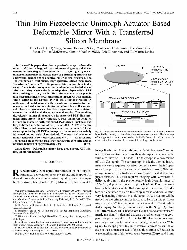
Fig. 1. Large-area continuous membrane DM concept. The mirror membraneis backed by an array of piezoelectric unimorph microactuators. The advantageof this approach is that the small strains obtainable from a piezoelectric materialat modest voltages are translated into relatively large displacements.
image Earth-like planets orbiting in “habitable zones” aroundnearby stars and to characterize their atmospheres, if any, in thevisible to infrared (IR) bands. The telescope is a two-mirror,off-axis Cassegrain. The coronagraph inside the thermal instru-ment enclosure requires wavefront correction over the full aper-ture of the primary mirror and a deformable mirror (DM) witha large number of actuators and low stroke, located at a con-jugate surface. This task requires imaging with wavefront fi-delity equivalent to the phenomenally high dynamic range of
– , depending on the approach taken. Future ground-based observatories with 30–100-m apertures also seek to de-tect and characterize Earth-like exoplanets in addition to othervery demanding observations [2]. Large-stroke actuators will beneeded on the primary mirror in order to form an image. Theremay also be a DM in a conjugate plane to enable diffraction-lim-ited imaging. Similarly, missions such as the Single ApertureFar-Infrared (SAFIR) Observatory [3] and associated interfero-metric missions [4] demand extreme wavefront quality at cryo-genic temperatures of K. The SAFIR telescope is conceivedas a larger and colder version of the segmented James WebbSpace Telescope point-design. Wavefront correction will be oneach of the segments instead of the conjugate plane. Because thewavelength range of this telescope is between 20 and 1 mm,
YANG et al.: THIN-FILM PIEZOELECTRIC UNIMORPH ACTUATOR-BASED DM 1215
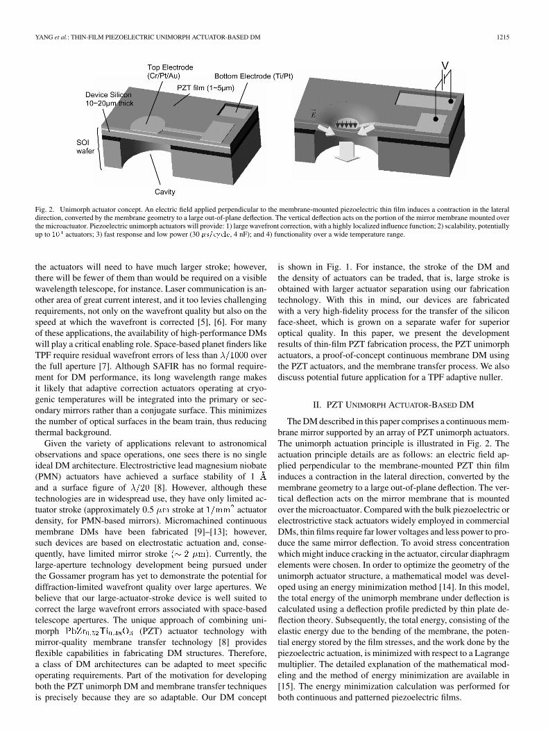
Fig. 2. Unimorph actuator concept. An electric field applied perpendicular to the membrane-mounted piezoelectric thin film induces a contraction in the lateraldirection, converted by the membrane geometry to a large out-of-plane deflection. The vertical deflection acts on the portion of the mirror membrane mounted overthe microactuator. Piezoelectric unimorph actuators will provide: 1) large wavefront correction, with a highly localized influence function; 2) scalability, potentiallyup to 10 actuators; 3) fast response and low power (30 �s=cycle, 4 nF); and 4) functionality over a wide temperature range.
the actuators will need to have much larger stroke; however,there will be fewer of them than would be required on a visiblewavelength telescope, for instance. Laser communication is an-other area of great current interest, and it too levies challengingrequirements, not only on the wavefront quality but also on thespeed at which the wavefront is corrected [5], [6]. For manyof these applications, the availability of high-performance DMswill play a critical enabling role. Space-based planet finders likeTPF require residual wavefront errors of less than overthe full aperture [7]. Although SAFIR has no formal require-ment for DM performance, its long wavelength range makesit likely that adaptive correction actuators operating at cryo-genic temperatures will be integrated into the primary or sec-ondary mirrors rather than a conjugate surface. This minimizesthe number of optical surfaces in the beam train, thus reducingthermal background.
Given the variety of applications relevant to astronomicalobservations and space operations, one sees there is no singleideal DM architecture. Electrostrictive lead magnesium niobate(PMN) actuators have achieved a surface stability of 1and a surface figure of [8]. However, although thesetechnologies are in widespread use, they have only limited ac-tuator stroke (approximately 0.5 stroke at actuatordensity, for PMN-based mirrors). Micromachined continuousmembrane DMs have been fabricated [9]–[13]; however,such devices are based on electrostatic actuation and, conse-quently, have limited mirror stroke . Currently, thelarge-aperture technology development being pursued underthe Gossamer program has yet to demonstrate the potential fordiffraction-limited wavefront quality over large apertures. Webelieve that our large-actuator-stroke device is well suited tocorrect the large wavefront errors associated with space-basedtelescope apertures. The unique approach of combining uni-morph (PZT) actuator technology withmirror-quality membrane transfer technology [8] providesflexible capabilities in fabricating DM structures. Therefore,a class of DM architectures can be adapted to meet specificoperating requirements. Part of the motivation for developingboth the PZT unimorph DM and membrane transfer techniquesis precisely because they are so adaptable. Our DM concept
is shown in Fig. 1. For instance, the stroke of the DM andthe density of actuators can be traded, that is, large stroke isobtained with larger actuator separation using our fabricationtechnology. With this in mind, our devices are fabricatedwith a very high-fidelity process for the transfer of the siliconface-sheet, which is grown on a separate wafer for superioroptical quality. In this paper, we present the developmentresults of thin-film PZT fabrication process, the PZT unimorphactuators, a proof-of-concept continuous membrane DM usingthe PZT actuators, and the membrane transfer process. We alsodiscuss potential future application for a TPF adaptive nuller.
II. PZT UNIMORPH ACTUATOR-BASED DM
The DM described in this paper comprises a continuous mem-brane mirror supported by an array of PZT unimorph actuators.The unimorph actuation principle is illustrated in Fig. 2. Theactuation principle details are as follows: an electric field ap-plied perpendicular to the membrane-mounted PZT thin filminduces a contraction in the lateral direction, converted by themembrane geometry to a large out-of-plane deflection. The ver-tical deflection acts on the mirror membrane that is mountedover the microactuator. Compared with the bulk piezoelectric orelectrostrictive stack actuators widely employed in commercialDMs, thin films require far lower voltages and less power to pro-duce the same mirror deflection. To avoid stress concentrationwhich might induce cracking in the actuator, circular diaphragmelements were chosen. In order to optimize the geometry of theunimorph actuator structure, a mathematical model was devel-oped using an energy minimization method [14]. In this model,the total energy of the unimorph membrane under deflection iscalculated using a deflection profile predicted by thin plate de-flection theory. Subsequently, the total energy, consisting of theelastic energy due to the bending of the membrane, the poten-tial energy stored by the film stresses, and the work done by thepiezoelectric actuation, is minimized with respect to a Lagrangemultiplier. The detailed explanation of the mathematical mod-eling and the method of energy minimization are available in[15]. The energy minimization calculation was performed forboth continuous and patterned piezoelectric films.
1216 JOURNAL OF MICROELECTROMECHANICAL SYSTEMS, VOL. 15, NO. 5, OCTOBER 2006
III. FABRICATION AND CHARACTERIZATION
Here, the fabrication and characterization processes aredescribed. The membrane transfer process [8] is used totransfer a silicon membrane onto the PZT unimorph actu-ator array. Section III-A describes the PZT film developmentprocess including its fabrication and analysis. The actuatorarray is prepared on an electroded substrate using the chem-ical-solution-deposited PZT films. Section III-B describes thefabrication and characterization processes for the unimorphactuator arrays using the PZT film technology described inSection III-A. Section III-C describes the wafer-scale transferprocess of single-crystal silicon mirror membranes onto thefabricated actuator array described in Section III-B, as wellas the results of surface figure characterization for the mirrormembrane.
A. Thin Film PZT: Deposition and Characterization
For this study, thin PZT films were prepared using a chemicalsolution deposition process. The procedure has been describedin detail elsewhere [16]. Briefly, the procedure used was amodification of that first introduced by Budd et al. [17] forprocessing of PZT films thick. Lead acetate trihy-drate, zirconium -propoxide, and titanium isopropoxide wereused as the precursors, while 2-methoxyethanol (2-MOE) wasthe primary solvent. After dissolution, the lead precursor wasdehydrated under vacuum. A mixture of zirconium -propoxideand titanium iso-propoxide in 2-MOE at room temperaturewas added and the entire solution was refluxed for 2 h underAr at 120 . After a second vacuum distillation, 2-MOE wasadded. The solution was then modified with acetylacetone (20vol%) and acetic acid (5 vol%). The final solution was 0.70Mwith 20mol% Pb in excess of stoichiometry to compensatefor high Pb volatility. The substrates used in this study werecommercially manufactured Pt(111)/Ti/ /Si wafers (NovaElectronic Materials, Inc., Richardson, TX) for electrical char-acterization and platinum-coated silicon on insulator (SOI)wafers for device fabrication. Prior to deposition of the PZTfilm, substrates were pre-annealed at 500 for 60 secondsto clean the surface. Solutions were dispensed through a sy-ringe with a 0.1- Whatman filter (Aldrich Chemical Co.,Milwaukee, WI) and the substrate was spun at 1500 rpm for30 s using a photoresist spinner (Headway Research, Inc.,Garland, TX). The majority of the organics were removed intwo pyrolysis steps, each 60 s in duration, on a hot plate at350 and 500 , respectively. During the second treatment,a 1-mm-thick aluminum plate was positioned parallel to andabout 3.5 mm above the film surface to enhance heating. Acrystallization anneal was performed after deposition of eachlayer in a Heatpulse 610 rapid thermal processing unit (AGAssociates, Sunnyvale, CA) at 700 for 60 s. Each sequenceproduced a layer approximately 0.20 in thickness, and thesequence was repeated to obtain the desired film thickness.
X-ray diffraction with Ni-filtered Cu radiation wasperformed to characterize the orientation and crystal structureof the PZT films (Scintag, Inc., Sunnyvale, CA). Microstruc-tural features of the films were examined using an S-3500Nscanning electron microscope (SEM) (Hitachi LtD., Tokyo,
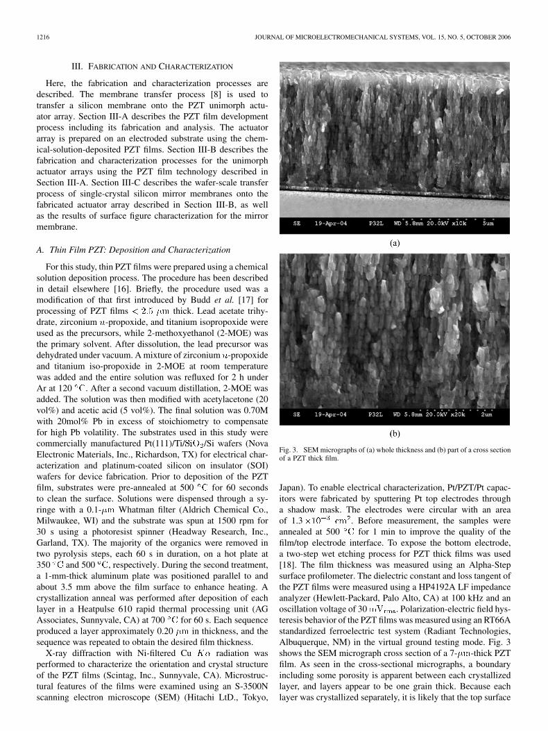
Fig. 3. SEM micrographs of (a) whole thickness and (b) part of a cross sectionof a PZT thick film.
Japan). To enable electrical characterization, Pt/PZT/Pt capac-itors were fabricated by sputtering Pt top electrodes througha shadow mask. The electrodes were circular with an areaof 1.3 . Before measurement, the samples wereannealed at 500 for 1 min to improve the quality of thefilm/top electrode interface. To expose the bottom electrode,a two-step wet etching process for PZT thick films was used[18]. The film thickness was measured using an Alpha-Stepsurface profilometer. The dielectric constant and loss tangent ofthe PZT films were measured using a HP4192A LF impedanceanalyzer (Hewlett-Packard, Palo Alto, CA) at 100 kHz and anoscillation voltage of 30 . Polarization-electric field hys-teresis behavior of the PZT films was measured using an RT66Astandardized ferroelectric test system (Radiant Technologies,Albuquerque, NM) in the virtual ground testing mode. Fig. 3shows the SEM micrograph cross section of a 7- -thick PZTfilm. As seen in the cross-sectional micrographs, a boundaryincluding some porosity is apparent between each crystallizedlayer, and layers appear to be one grain thick. Because eachlayer was crystallized separately, it is likely that the top surface
YANG et al.: THIN-FILM PIEZOELECTRIC UNIMORPH ACTUATOR-BASED DM 1217
Fig. 4. XRD patterns for PZT films with different thickness. The peaks areindexed in terms of a pseudocubic perovskite structure.
Fig. 5. Polarization-Electric field hysteresis loop for a 1-�m-thick PZT film.Good saturation is apparent.
of each layer provided nucleation sites for the layer above it.The grain size is relatively uniform in plane and is about 150nm. XRD measurements showed that the films were phase-pureperovskite (i.e., no pyrochlore phase was identified), and hada gradual change in the preferred orientation with increasingfilm thickness (Fig. 4). When the film was thin , thePZT films had (111) preferred orientation on (111) orientedplatinum coated substrates, indicating a predominance ofnucleation from the bottom electrode. With increasing filmthickness, the films became more and more randomly orientedas the influence of the Pt/PZT interface was reduced [19].Fig. 5 shows a polarization-electric field hysteresis loop of a1- -thick PZT film. The polarization versus applied electricfield loop shows a good square shape. Remanent polarization
and coercive field values extracted from the P-Ehysteresis loop are 36 and 51 kV/cm, respectively.The relative permittivity and tangent loss for a 1- -thick PZTfilm are about 1040 and 2.5% at room temperature, respec-tively. These values are characteristic of a high-quality film. For
Fig. 6. Flowchart for the preparation of doped PZT films.
Fig. 7. X-ray diffraction patterns for Mg- and Sr-doped PZT thin films. Dopinghas little influence on either the film crystallinity or orientation.
applications of DMs, there is interest in the low-temperatureproperties of the piezoelectric film. In particular, since theultimate application of the mirrors will be in space, operationat cryogenic temperatures is important. For this reason, severaldopants for the PZT films were investigated to determine ifsuperior low-temperature performance could be achieved.
Due to the divergence in the permittivity near a phasetransition, the piezoelectric properties increase as the tran-sition is approached, providing that a well-poled state canbe maintained. Thus, lower transition temperatures should
1218 JOURNAL OF MICROELECTROMECHANICAL SYSTEMS, VOL. 15, NO. 5, OCTOBER 2006
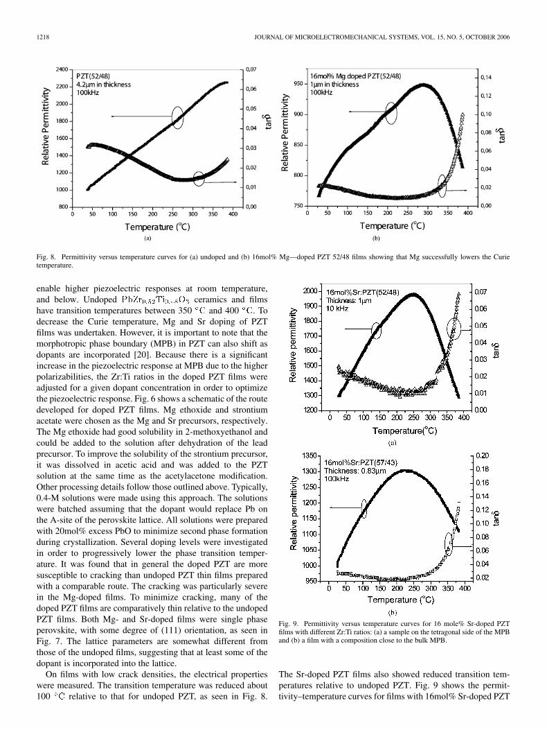
Fig. 8. Permittivity versus temperature curves for (a) undoped and (b) 16mol% Mg—doped PZT 52/48 films showing that Mg successfully lowers the Curietemperature.
enable higher piezoelectric responses at room temperature,and below. Undoped ceramics and filmshave transition temperatures between 350 and 400 . Todecrease the Curie temperature, Mg and Sr doping of PZTfilms was undertaken. However, it is important to note that themorphotropic phase boundary (MPB) in PZT can also shift asdopants are incorporated [20]. Because there is a significantincrease in the piezoelectric response at MPB due to the higherpolarizabilities, the Zr:Ti ratios in the doped PZT films wereadjusted for a given dopant concentration in order to optimizethe piezoelectric response. Fig. 6 shows a schematic of the routedeveloped for doped PZT films. Mg ethoxide and strontiumacetate were chosen as the Mg and Sr precursors, respectively.The Mg ethoxide had good solubility in 2-methoxyethanol andcould be added to the solution after dehydration of the leadprecursor. To improve the solubility of the strontium precursor,it was dissolved in acetic acid and was added to the PZTsolution at the same time as the acetylacetone modification.Other processing details follow those outlined above. Typically,0.4-M solutions were made using this approach. The solutionswere batched assuming that the dopant would replace Pb onthe A-site of the perovskite lattice. All solutions were preparedwith 20mol% excess PbO to minimize second phase formationduring crystallization. Several doping levels were investigatedin order to progressively lower the phase transition temper-ature. It was found that in general the doped PZT are moresusceptible to cracking than undoped PZT thin films preparedwith a comparable route. The cracking was particularly severein the Mg-doped films. To minimize cracking, many of thedoped PZT films are comparatively thin relative to the undopedPZT films. Both Mg- and Sr-doped films were single phaseperovskite, with some degree of (111) orientation, as seen inFig. 7. The lattice parameters are somewhat different fromthose of the undoped films, suggesting that at least some of thedopant is incorporated into the lattice.
On films with low crack densities, the electrical propertieswere measured. The transition temperature was reduced about100 relative to that for undoped PZT, as seen in Fig. 8.
Fig. 9. Permittivity versus temperature curves for 16 mole% Sr-doped PZTfilms with different Zr:Ti ratios: (a) a sample on the tetragonal side of the MPBand (b) a film with a composition close to the bulk MPB.
The Sr-doped PZT films also showed reduced transition tem-peratures relative to undoped PZT. Fig. 9 shows the permit-tivity–temperature curves for films with 16mol% Sr-doped PZT
YANG et al.: THIN-FILM PIEZOELECTRIC UNIMORPH ACTUATOR-BASED DM 1219
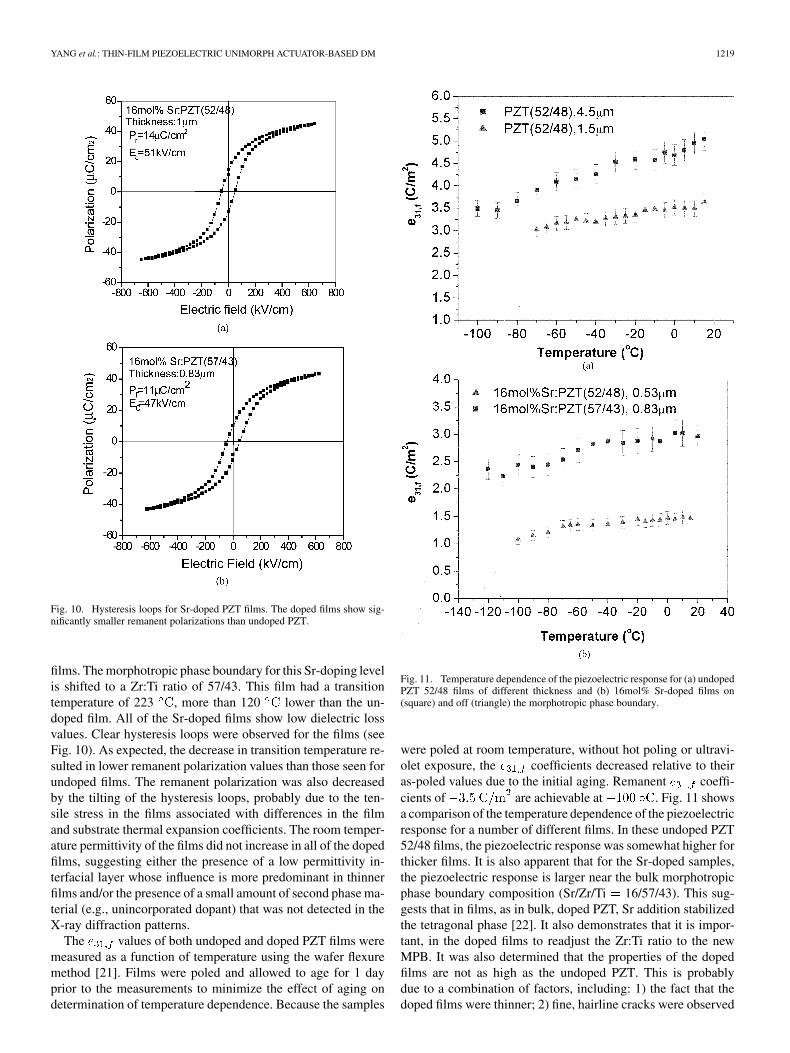
Fig. 10. Hysteresis loops for Sr-doped PZT films. The doped films show sig-nificantly smaller remanent polarizations than undoped PZT.
films. The morphotropic phase boundary for this Sr-doping levelis shifted to a Zr:Ti ratio of 57/43. This film had a transitiontemperature of 223 , more than 120 lower than the un-doped film. All of the Sr-doped films show low dielectric lossvalues. Clear hysteresis loops were observed for the films (seeFig. 10). As expected, the decrease in transition temperature re-sulted in lower remanent polarization values than those seen forundoped films. The remanent polarization was also decreasedby the tilting of the hysteresis loops, probably due to the ten-sile stress in the films associated with differences in the filmand substrate thermal expansion coefficients. The room temper-ature permittivity of the films did not increase in all of the dopedfilms, suggesting either the presence of a low permittivity in-terfacial layer whose influence is more predominant in thinnerfilms and/or the presence of a small amount of second phase ma-terial (e.g., unincorporated dopant) that was not detected in theX-ray diffraction patterns.
The values of both undoped and doped PZT films weremeasured as a function of temperature using the wafer flexuremethod [21]. Films were poled and allowed to age for 1 dayprior to the measurements to minimize the effect of aging ondetermination of temperature dependence. Because the samples
Fig. 11. Temperature dependence of the piezoelectric response for (a) undopedPZT 52/48 films of different thickness and (b) 16mol% Sr-doped films on(square) and off (triangle) the morphotropic phase boundary.
were poled at room temperature, without hot poling or ultravi-olet exposure, the coefficients decreased relative to theiras-poled values due to the initial aging. Remanent coeffi-cients of are achievable at . Fig. 11 showsa comparison of the temperature dependence of the piezoelectricresponse for a number of different films. In these undoped PZT52/48 films, the piezoelectric response was somewhat higher forthicker films. It is also apparent that for the Sr-doped samples,the piezoelectric response is larger near the bulk morphotropicphase boundary composition (Sr/Zr/Ti 16/57/43). This sug-gests that in films, as in bulk, doped PZT, Sr addition stabilizedthe tetragonal phase [22]. It also demonstrates that it is impor-tant, in the doped films to readjust the Zr:Ti ratio to the newMPB. It was also determined that the properties of the dopedfilms are not as high as the undoped PZT. This is probablydue to a combination of factors, including: 1) the fact that thedoped films were thinner; 2) fine, hairline cracks were observed
1220 JOURNAL OF MICROELECTROMECHANICAL SYSTEMS, VOL. 15, NO. 5, OCTOBER 2006
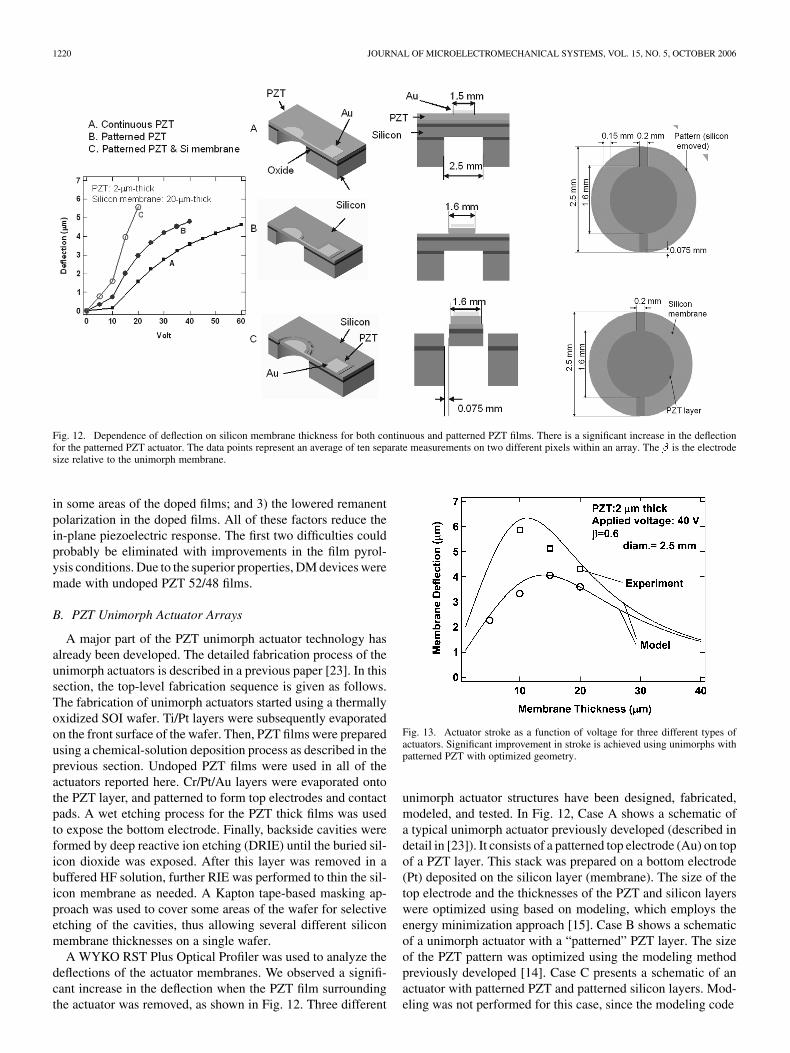
Fig. 12. Dependence of deflection on silicon membrane thickness for both continuous and patterned PZT films. There is a significant increase in the deflectionfor the patterned PZT actuator. The data points represent an average of ten separate measurements on two different pixels within an array. The � is the electrodesize relative to the unimorph membrane.
in some areas of the doped films; and 3) the lowered remanentpolarization in the doped films. All of these factors reduce thein-plane piezoelectric response. The first two difficulties couldprobably be eliminated with improvements in the film pyrol-ysis conditions. Due to the superior properties, DM devices weremade with undoped PZT 52/48 films.
B. PZT Unimorph Actuator Arrays
A major part of the PZT unimorph actuator technology hasalready been developed. The detailed fabrication process of theunimorph actuators is described in a previous paper [23]. In thissection, the top-level fabrication sequence is given as follows.The fabrication of unimorph actuators started using a thermallyoxidized SOI wafer. Ti/Pt layers were subsequently evaporatedon the front surface of the wafer. Then, PZT films were preparedusing a chemical-solution deposition process as described in theprevious section. Undoped PZT films were used in all of theactuators reported here. Cr/Pt/Au layers were evaporated ontothe PZT layer, and patterned to form top electrodes and contactpads. A wet etching process for the PZT thick films was usedto expose the bottom electrode. Finally, backside cavities wereformed by deep reactive ion etching (DRIE) until the buried sil-icon dioxide was exposed. After this layer was removed in abuffered HF solution, further RIE was performed to thin the sil-icon membrane as needed. A Kapton tape-based masking ap-proach was used to cover some areas of the wafer for selectiveetching of the cavities, thus allowing several different siliconmembrane thicknesses on a single wafer.
A WYKO RST Plus Optical Profiler was used to analyze thedeflections of the actuator membranes. We observed a signifi-cant increase in the deflection when the PZT film surroundingthe actuator was removed, as shown in Fig. 12. Three different
Fig. 13. Actuator stroke as a function of voltage for three different types ofactuators. Significant improvement in stroke is achieved using unimorphs withpatterned PZT with optimized geometry.
unimorph actuator structures have been designed, fabricated,modeled, and tested. In Fig. 12, Case A shows a schematic ofa typical unimorph actuator previously developed (described indetail in [23]). It consists of a patterned top electrode (Au) on topof a PZT layer. This stack was prepared on a bottom electrode(Pt) deposited on the silicon layer (membrane). The size of thetop electrode and the thicknesses of the PZT and silicon layerswere optimized using based on modeling, which employs theenergy minimization approach [15]. Case B shows a schematicof a unimorph actuator with a “patterned” PZT layer. The sizeof the PZT pattern was optimized using the modeling methodpreviously developed [14]. Case C presents a schematic of anactuator with patterned PZT and patterned silicon layers. Mod-eling was not performed for this case, since the modeling code
YANG et al.: THIN-FILM PIEZOELECTRIC UNIMORPH ACTUATOR-BASED DM 1221
Fig. 14. Process schematic for fabrication and transfer of a mirror membrane.
was not optimized for patterned (noncontinuous) silicon struc-tures. Finite-element model (FEM) analysis may be requiredin order to accurately assess the actuator behavior for Case C,but this would be beyond the scope of the work described inthis paper. The measured deflection for an optimized actuator is
5.7 at 20 V (for an actuator with a 2.5-mm diameter, PZT/Si- - -thick, PZT patterned over 60% of the mem-
brane diameter, and silicon membrane patterned). This deflec-tion increase is believed to be due to a decrease in the residualstress in the actuator.
1222 JOURNAL OF MICROELECTROMECHANICAL SYSTEMS, VOL. 15, NO. 5, OCTOBER 2006
In order to maximize the deflection, unimorph actuators withdifferent silicon membrane thicknesses were characterized. Ac-tuators with different membrane thicknesses were obtained onthe same wafer by selectively etching the silicon membrane todifferent final thicknesses using the Kapton tape-masked back-side etching process [23]. Fig. 13 compares the measured ac-tuator strokes with the modeled values. The actuation resultsfrom using 2.5-mm-diameter membrane actuators with: 1) con-tinuous PZT film (i.e., Case A) and 2) patterned PZT film (i.e.,Case B) are shown as a function of membrane thickness. Theexperimental results are superimposed over their respective pre-dicted deflection curves from the simulation model. As pre-dicted by our model, the maximum deflections were obtained atintermediate silicon-membrane thicknesses of approximately:1) 15 with the continuous PZT film and 2) 10 withthe patterned PZT film.
C. Deformable Mirror
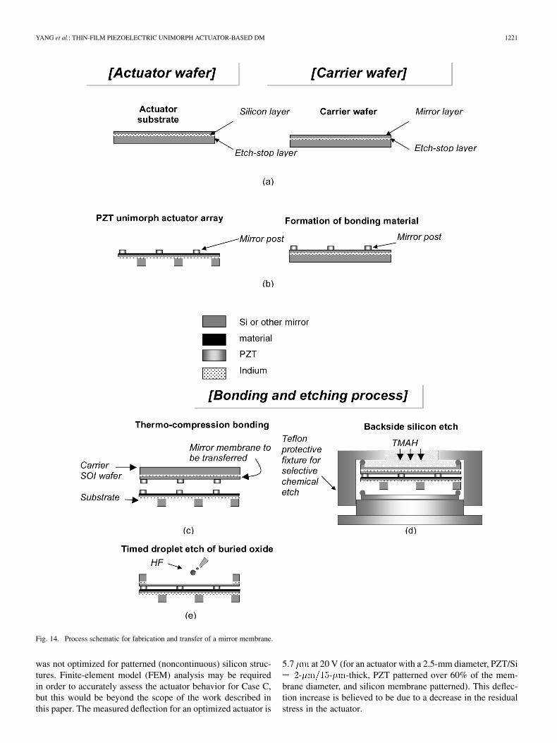
A proof-of-concept DM structure was fabricated using typicalunimorph actuators (Case A in Fig. 12), and its actuation per-formance was characterized using the WYKO RST Plus OpticalProfiler. For fabrication of the mirror membrane, we utilizedthe membrane transfer process [8] developed at JPL in orderto transfer the mirror membrane onto the fabricated actuator ar-rays. The membrane transfer process is briefly described as fol-lows. The mirror membrane transfer process involves transferof the single-crystal silicon layer from the SOI wafer followingthe metallization, bonding, and etching processes. SOI carrierwafers were used for the fabrication of the single-crystal siliconmirror membrane. The thickness of the transferred membraneis determined by the thickness of the SOI top silicon layer. A20- -thick single-crystal silicon mirror membrane was trans-ferred onto the actuator wafer. The actuator wafer and the SOIcarrier wafer were prepared [see Fig. 14(a)]. Cr/Pt/Au metallayers were deposited and patterned to form bonding pad ar-rays on both the carrier and actuator wafers. A 1- -thick Inlayer and a 100-Å-thick Au layer were subsequently depositedand patterned on both the carrier and actuator wafers using alift-off process [see Fig. 14(b)]. The SOI carrier wafer was sub-sequently bonded to the substrate wafer [see Fig. 14(c)]. Thebackside etching was conducted in a 25 wt% solution of tetram-ethylammonium hydroxide (TMAH) at 80 until the buriedoxide was exposed. A specially designed Teflon fixture was usedto protect both the backside of the bonded substrate wafer aswell as the bonded interface [see Fig. 14(d)]. The exposed oxidewas removed by using 49% HF droplets [see Fig. 14(e)]. Anplasma etch was incorporated, as necessary, to selectively etchthe transferred membrane in order to release membrane struc-tures [see Fig. 14(f)].
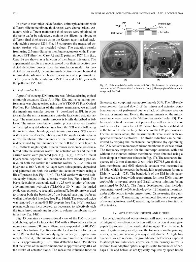
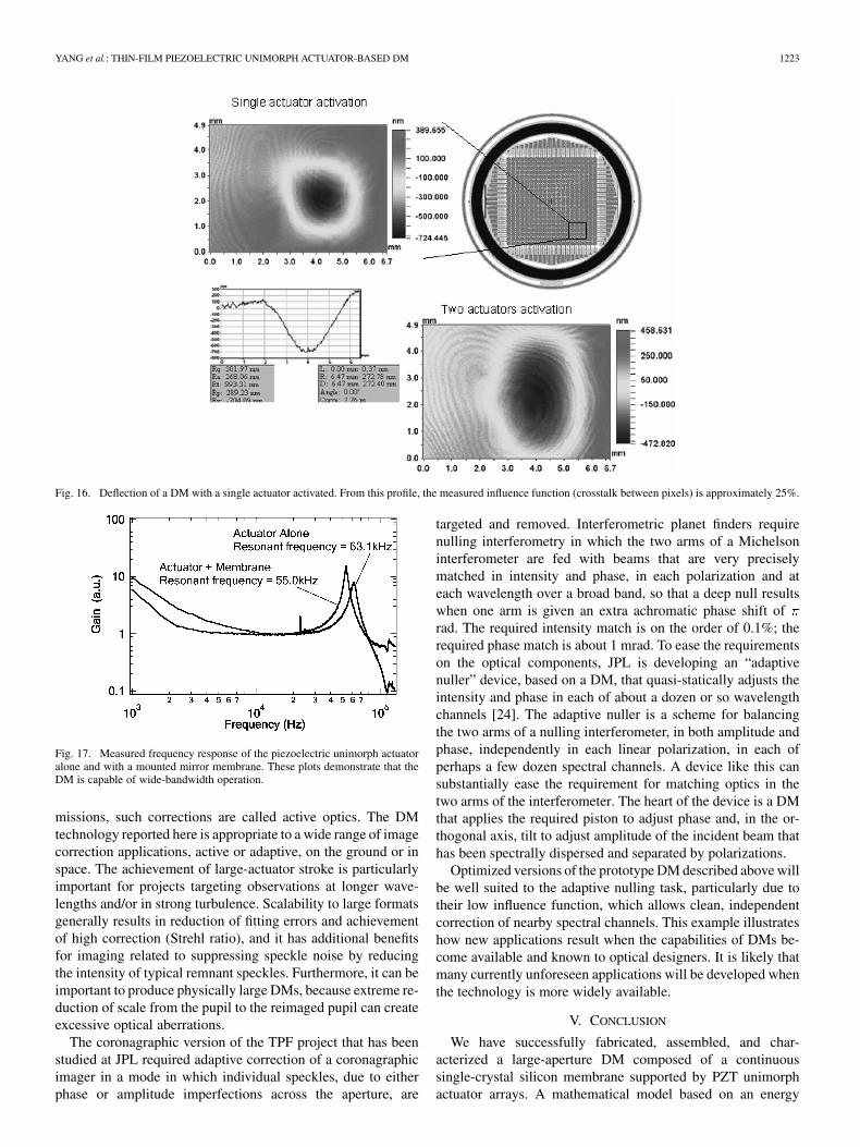
Fig. 15 contains a cross-sectional view of the DM structureand photographs of a fabricated DM with a 20- -thick siliconmembrane mirror (50 mm 50 mm area) supported by 400 PZTunimorph actuators. Fig. 16 shows the local surface deformationof a DM created by the underlying actuators (i.e., typical uni-morph: Case A). The measured maximum mirror deflection at30 V is approximately 1 . This deflection for a DM showsthat the stroke of the mirror membrane is approximately 40% ofthe stroke of actuator alone. The measured influence function
Fig. 15. Fabricated deformable mirror with 20� 20 piezoelectric unimorph ac-tuator array. (a) Cross-sectional schematic. (b), (c) Photographs of the actuatorarrays and the DM.
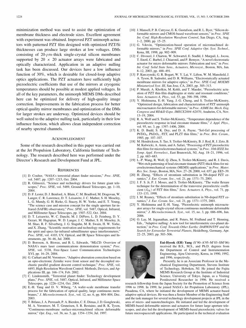
(interactuator coupling) was approximately 30%. The full-scalemeasurement (up and down) of the mirror and actuator com-bination was not performed due to a lack of reference area onthe mirror membrane. Hence, the measurements on the mirrormembrane were made in the “differential mode” only [23]. Thefull-scale optical measurement protocol as well as the softwareand driver electronics for a DM device have to be establishedin the future in order to fully characterize the DM performance.For the actuator alone, the measurements were made with re-spect to reference electrodes. The stroke reduction can be min-imized by varying the mechanical compliance (by optimizingthe PZT/ actuator membrane/ mirror membrane thickness ratio).The frequency responses for the unimorph actuator, with andwithout the mounted mirror membrane, were obtained using alaser-doppler vibrometer (shown in Fig. 17). The resonance fre-quency of a 2-mm-diameter, 2- -thick PZT/15- -thick sil-icon membrane, and 60% electrode actuator was measured at63 kHz, which far exceeds the bandwidth requirement for mostDMs [23]. The bandwidth of the DM in this paperfar exceeds the bandwidth requirement for most DMs that areapplicable to several space and Earth science missions beingenvisioned by NASA. The future development plan includesdemonstration of the DM technology by: 1) flattening the mirrorunder a Michelson interferometer setup; 2) measuring the gainsof all actuators; 3) measuring the temporal frequency responseof several actuators; and 4) measuring the influence function ofall actuators.
IV. APPLICATIONS: PRESENT AND FUTURE
Large ground-based observatories will need a combinationof integrated wavefront correction with correction at conjugatepupils to produce diffraction-limited imagery. The use of suchcontrol systems may greatly ease the tolerances on the primarymirror, which are generally a major cost driver. At high fre-quencies, as are relevant for ground-based telescopes exposedto atmospheric turbulence, correction of the primary mirror isreferred to as adaptive optics; at quasi-static frequencies of per-haps 1 Hz and below, as are typically required by space-based
YANG et al.: THIN-FILM PIEZOELECTRIC UNIMORPH ACTUATOR-BASED DM 1223
Fig. 16. Deflection of a DM with a single actuator activated. From this profile, the measured influence function (crosstalk between pixels) is approximately 25%.
Fig. 17. Measured frequency response of the piezoelectric unimorph actuatoralone and with a mounted mirror membrane. These plots demonstrate that theDM is capable of wide-bandwidth operation.
missions, such corrections are called active optics. The DMtechnology reported here is appropriate to a wide range of imagecorrection applications, active or adaptive, on the ground or inspace. The achievement of large-actuator stroke is particularlyimportant for projects targeting observations at longer wave-lengths and/or in strong turbulence. Scalability to large formatsgenerally results in reduction of fitting errors and achievementof high correction (Strehl ratio), and it has additional benefitsfor imaging related to suppressing speckle noise by reducingthe intensity of typical remnant speckles. Furthermore, it can beimportant to produce physically large DMs, because extreme re-duction of scale from the pupil to the reimaged pupil can createexcessive optical aberrations.
The coronagraphic version of the TPF project that has beenstudied at JPL required adaptive correction of a coronagraphicimager in a mode in which individual speckles, due to eitherphase or amplitude imperfections across the aperture, are
targeted and removed. Interferometric planet finders requirenulling interferometry in which the two arms of a Michelsoninterferometer are fed with beams that are very preciselymatched in intensity and phase, in each polarization and ateach wavelength over a broad band, so that a deep null resultswhen one arm is given an extra achromatic phase shift ofrad. The required intensity match is on the order of 0.1%; therequired phase match is about 1 mrad. To ease the requirementson the optical components, JPL is developing an “adaptivenuller” device, based on a DM, that quasi-statically adjusts theintensity and phase in each of about a dozen or so wavelengthchannels [24]. The adaptive nuller is a scheme for balancingthe two arms of a nulling interferometer, in both amplitude andphase, independently in each linear polarization, in each ofperhaps a few dozen spectral channels. A device like this cansubstantially ease the requirement for matching optics in thetwo arms of the interferometer. The heart of the device is a DMthat applies the required piston to adjust phase and, in the or-thogonal axis, tilt to adjust amplitude of the incident beam thathas been spectrally dispersed and separated by polarizations.
Optimized versions of the prototype DM described above willbe well suited to the adaptive nulling task, particularly due totheir low influence function, which allows clean, independentcorrection of nearby spectral channels. This example illustrateshow new applications result when the capabilities of DMs be-come available and known to optical designers. It is likely thatmany currently unforeseen applications will be developed whenthe technology is more widely available.
V. CONCLUSION
We have successfully fabricated, assembled, and char-acterized a large-aperture DM composed of a continuoussingle-crystal silicon membrane supported by PZT unimorphactuator arrays. A mathematical model based on an energy
1224 JOURNAL OF MICROELECTROMECHANICAL SYSTEMS, VOL. 15, NO. 5, OCTOBER 2006
minimization method was used to assist the optimization ofmembrane thickness and electrode sizes. Excellent agreementwith experiment was obtained. Improved PZT unimorph actua-tors with patterned PZT film designed with optimized PZT/Sithicknesses can produce large strokes at low voltages. DMsconsisting of 20- -thick single-crystal silicon membranessupported by 20 20 actuator arrays were fabricated andoptically characterized. Application in an adaptive nullingtask has been discussed. Our devices have a low influencefunction of 30%, which is desirable for closed-loop adaptiveoptics applications. The PZT actuators have sufficiently highpiezoelectric coefficients that use of the mirrors at cryogenictemperatures should be possible at modest applied voltages. Inall of the key parameters, the unimorph MEMS DMs describedhere can be optimized for delivery of high-quality imagecorrection. Improvements in the fabrication process for betteroptical quality mirror membranes and optimization of the DMsfor larger strokes are underway. Optimized devices should bewell suited to the adaptive nulling task, particularly in their lowinfluence function, which allows clean independent correctionof nearby spectral channels.
ACKNOWLEDGMENT
Some of the research described in this paper was carried outat the Jet Propulsion Laboratory, California Institute of Tech-nology. The research described here was performed under theDirector’s Research and Development Fund at JPL.
REFERENCES
[1] D. Coulter, “NASA’s terrestrial planet finder missions,” Proc. SPIE,vol. 5487, pp. 1207–1215, Oct. 2004.
[2] R. Gilmozzi, “Science and technology drivers for future giant tele-scopes,” Proc. SPIE, vol. 5489, Ground-Based Telescopes, pp. 1–10,2004.
[3] D. F. Lester, D. J. Benford, A. Blain, C. M. Bradford, M. Dragovan, W.Langer, C. R. Lawrence, D. T. Leisawitz, J. C. Mather, S. H. Moseley,L. G. Mundy, G. H. Rieke, G. Stacey, H. W. Yorke, and E. T. Young,“The science case and mission concept for the single aperture far-in-frared (SAFIR) observatory,” Proc. SPIE, vol. 5487, Optical, Infrared,and Millimeter Space Telescopes, pp. 1507–522, Oct. 2004.
[4] D. T. Leisawitz, W. C. Danchi, M. J. DiPirro, L. D. Feinberg, D. Y.Gezari, M. Hagopian, W. D. Langer, J. C. Mather, S. H. Moseley, Jr,M. Shao, R. F. Silverberg, J. G. Staguhn, M. R. Swain, H. W. Yorke,and X. Zhang, “Scientific motivation and technology requirements forthe spirit and specs far-infrared submillimeter space interferometers,”Proc. SPIE, vol. 4103, UV, Optical, and IR Space Telescopes and In-struments, pp. 36–46, Jul. 2000.
[5] D. Boroson, A. Biswas, and B. L. Edwards, “MLCD: Overview ofNASA’s mars laser communications demonstration system,” Proc.SPIE, vol. 5338, Free-Space Laser Communication TechnologiesXVI, pp. 16–29, 2004.
[6] G. Carhart and M. Vorontsov, “Adaptive aberration correction based onan opto-electronic Zernike wave front sensor and the decoupled sto-chastic parallel gradient descent control technique,” Proc. SPIE, vol.4493, High-Resolution Wavefront Control: Methods, Devices, and Ap-plications III, pp. 166–174, Feb. 2002.
[7] C. Lindensmith, “Terrestrial planet finder: Technology developmentplans,” Proc. SPIE, vol. 5487, Optical, Infrared, and Millimeter SpaceTelescopes, pp. 1226–1234, Oct. 2004.
[8] E.-H. Yang and D. V. Wiberg, “A wafer-scale membrane transferprocess for the fabrication of optical quality, large continuous mem-branes,” J. Microelectromech. Syst., vol. 12, no. 6, pp. 804–804, Dec.2003.
[9] T. Bifano, J. A. Perreault, P. A. Bierden, C. E. Dimas, J. D. Gonglewski,M. A. Vorontsov, M. T. Gruneisen, S. R. Restaino, and R. K. Tyson,“Continuous-membrane surface-micromachined silicon deformablemirror,” Opt. Eng., vol. 36, no. 5, pp. 1354–1354, Jul. 1997.
[10] J. Mansell, P. B. Catrysse, E. K. Gustafson, and R. L. Byer, “Silicon de-formable mirrors and CMOS-based wavefront sensors,” in Proc. SPIEInt. Conf. High-Resolution Wavefront Control, San Diego, CA, Aug.1–2, 2000, pp. 15–25.
[11] G. Vdovin, “Optimization-based operation of micromachined de-formable mirrors,” in Proc. SPIE Conf. Adaptive Opt. Syst. Technol.,Kona, HI, 1998, pp. 902–909.
[12] C. Divouxl, J. Charton, W. Schwartzl, E. Stadld, J. Margail, L. Jocou,T. Enotl, C. Barbel, J. Chiaronil, and P. Bemyer, “A novel electrostaticactuator for micro deformable mirrors: Fabrication and test,” in Proc.Int. Conf. Solid State Sens., Actuators, Microsyst., Boston, MA, Jun.8–12, 2003, pp. 488–491.
[13] P. Kurczynski, G. R. Bogart, W. Y. Lai, V. Lifton, W. M. Mansfield, J.A. Tyson, B. Sadoulet, and D. R. Williams, “Electrostatically actuatedmembrane mirrors for adaptive optics,” in Proc. SPIE Conf. MOEMSMiniaturized Syst. III, San Jose, CA, 2003, pp. 305–313.
[14] P. Muralt, A. Kholkin, M. Kohli, and T. Maeder, “Piezoelectric actu-ation of PZT thin-film diaphragms at static and resonant conditions,”Sens. Actuators A, Phys., vol. 53, pp. 398–398, 1996.
[15] Y. Hishinuma, E.-H. Yang, J.-G. Cheng, and S. Trolier-McKinstry,“Optimized design, fabrication and characterization of PZT unimorphmicroactuators for deformable mirrors,” in Proc. ASME Int. Mech. Eng.Congress and RD&D Expo. IMECE2004–62070, Anaheim, CA, Nov.13–19, 2004.
[16] R. A. Wolf and S. Trolier-McKinstry, “Temperature dependence of thepiezoelectric response in lead zirconate titanate films,” J. Appl. Phys.,vol. 95, no. 3, pp. 1397–1406, 2004.
[17] K. D. Budd, S. K. Dey, and D. A. Payne, “Sol-Gel processing ofPbTiO , PbZrO , PZT, and PLZT thin films,” in Proc. Brit. Ceram.,1985, pp. 107–107.
[18] M. Hendrickson, S. Tao, S. Trolier-McKinstry, B. J. Rod, R. J. Zeto, B.M. Kulwicki, A. Amin, and A. Safari, “Processing of PZT piezoelectricthin films for microelectromechanical systems,” in Proc. 10th IEEE Int.Symp. Appl. Ferroelect., East Brunswick, NJ, Aug. 18–21, 1996, vol.2, pp. 683–683.
[19] L.-P. Wang, R. Wolf, Q. Zhou, S. Trolier-McKinstry, and R. J. Davis,“Wet-etch patterning of lead zirconate titanate (PZT) thick films for mi-croelectromechanical systems (MEMS) applications,” in Proc. Mater.Res. Soc. Symp., Boston, MA, Nov. 27–28, 2000, vol. 657, pp. EE5–39.
[20] H. Zheng, “Effects of strontium substitution in Nb-doped PZT ce-ramics,” J. Eur. Ceram. Soc., vol. 21, pp. 1371–75, 2001.
[21] J. F. S. Jr, P. J. Moses, and S. Trolier-McKinstry, “The wafer flexuretechnique for the determination of the transverse piezoelectric coeffi-cient (d ) of PZT thin films,” Sens. Actuators A, Phys., vol. 71, pp.133–133, 1998.
[22] I. M. Reaney, “Effects of strontium substitution in Nb-doped PZT ce-ramics,” J. Eur. Ceram. Soc., vol. 21, pp. 1371–1375, 2001.
[23] Y. Hishinuma and E.-H. Yang, “Piezoelectric unimorph microactu-ator arrays for single-crystal silicon continuous membrane deformablemirror,” J. Microelectromech. Syst., vol. 15, no. 3, pp. 686–696, Jun.2006.
[24] O. Lay, M. Jeganathan, and R. Peters, M. Fridlund and T. Henning,Eds., “Adaptive nulling: A new tool for interferometric exo-planet de-tection,” in Proc. Conf. Towards Other Earths: DARWIN/TPF and theSearch for Extrasolar Terrestrial Planets, Heidelberg, Germany, Apr.22–25, 2003, pp. 503–506.
Eui-Hyeok (EH) Yang (S’90–A’95–M’03–SM’06)received the B.S., M.S., and Ph.D. degrees fromthe Department of Control and InstrumentationEngineering, Ajou University, Korea, in 1990, 1992,and 1996, respectively.
Presently, he is an Associate Professor in the Me-chanical Engineering Department, Stevens Instituteof Technology, Hoboken, NJ. He joined the FujitaMEMS Research Group at the Institute of IndustrialScience, University of Tokyo, Japan, as a VisitingPostdoctoral Researcher in 1996. He received a
research fellowship from the Japan Society for the Promotion of Science from1996 to 1998. In 1999, he joined NASA’s Jet Propulsion Laboratory (JPL),Pasadena, CA, where he initiated the development of MEMS actuator-basedadaptive optical devices. He was then a Senior Member of the Engineering Staffand the task manager for several technology development projects at JPL in thearea of micro- and nanotechnologies. He initiated and led the development ofMEMS-based deformable mirrors and actuators for future large aperture tele-scopes, and also led the development of MEMS-based piezoelectric valves forfuture microspacecraft applications. He participated in the technical evaluation
YANG et al.: THIN-FILM PIEZOELECTRIC UNIMORPH ACTUATOR-BASED DM 1225
of MEMS mirror array technologies developed for the Multi Object Spectrom-eter (MOS) project for the James Webb Space Telescope (JWST). He was atechnical monitor for a NASA SBIR project. He was a Research Adviser forNational Research Council (NRC) in the area of piezoelectric microactuatorsfor active-mirror technologies. He has been successful in winning extremelycompetitive major research grants which represents an exceptional achievementand productivity within NASA. He has extensive experience in microactuator,deformable mirror, and optical membrane fabrication. His current researchinterests include all aspects of microsensors/actuators, microfluidics, adaptiveoptics, micro/nano energy conversion, and nano-manufacturing technologies.He has published over 90 papers in the field of MEMS, and has six patentsissued or pending.
Dr. Yang is a member of the Technical Program Committee (TPC) of theIEEE Sensors Conference. He is Topic Organizer of the Micro and Nano De-vices Topic, within the MEMS Division, of the ASME International MechanicalEngineering Congress and Exposition. He has been serving as a referee for sev-eral archival journals, international conferences and proposals. In recognitionof his excellence in advancing the use of MEMS-based actuators for space ap-plications, he received the Lew Allen Award for Excellence for 2003 at JPL.
Yoshikazu Hishinuma received the B.S. degree inapplied and engineering physics from Cornell Uni-versity, Ithaca, NY, in 1997, and the M.S. and Ph.D.degrees in applied physics from Stanford University,Stanford, CA, in 1999 and 2002, respectively. Hisdoctoral work concentrated on experimental and the-oretical studies on refrigeration effect of low workfunction materials during electron tunneling at roomtemperature.
From 2002 to 2005, he was with the MicrodevicesLaboratory, Jet Propulsion Laboratory, Pasadena, CA
where his research focused on the development of micromachined deformablemirrors. Currently, he is with Fuji Photo Film Company, Ltd., Kanagawa, Japan,where he continues to work on various microscale devices. His research interestsinclude microfabrication technologies, MEMS actuator designs, and sensors forsmall-signal detections.
Jian-Gong Cheng received the M.S. degree incondensed-matter physics from Shandong Univer-sity, Jinan, China, in 1997, and the Ph.D. degreein microelectronics and solid-state electronics fromShanghai Institute of Technical Physics, ChineseAcademy of Sciences, Shanghai, China, in 2000.
He was a Senior Research Fellow with the Corpo-rate Technology of Siemens AG, Munich, Germany,from 2001 to 2002. He was with the Material Re-search Laboratory of Pennsylvania State Universityas a Postdoctoral Fellow from 2003 to 2005. Since
April 2005, he has been a Professor with the Shanghai Institute of Microsystemand Information Technology, Chinese Academy Sciences, Shanghai, China. Hisresearch covers ferroelectric materials and their applications as pyroelectrics ininfrared detectors, dielectrics in capacitors, and as piezoelectric transducers forbiosensors. He is pursuing his research interests in developing novel biosensors.
Susan Trolier-McKinstry (M’92–SM’01) receivedthe B.S., M.S., and Ph.D. degrees from the Pennsyl-vania State University (Penn State), University Park,all in ceramic science.
After graduation, she joined the faculty at PennState, where she is currently a Professor of ceramicscience and engineering and Director of the W.M. Keck Smart Materials Integration Laboratory.Her main research interests include dielectric andpiezoelectric thin films, the development of texturein bulk ceramic piezoelectrics, and spectroscopic
ellipsometry. She has held visiting appointments with the Hitachi CentralResearch Laboratory, the Army Research Laboratory, and the École Polytech-nique Federale de Lausanne.
Prof. Trolier-McKinstry is a Fellow of the American Ceramic Society and amember of the Materials Research Society. She is past-president of both Ker-amos and the Ceramics Education Council and is co-chair of the committeerevising the IEEE Standard on Ferroelectricity. She has served as Vice-Pres-ident for Ferroelectrics of the IEEE UFFC and is now President-Elect of thesociety. She was the recipient of the Robert Coble Award of the American Ce-ramic Society, the Wilson Award for Outstanding Teaching in the College ofEarth and Mineral Sciences, the Materials Research Laboratory OutstandingFaculty Award, and a National Science Foundation Career grant.
Eric Bloemhof received the Ph.D. degree in physicsfrom the University of California, Berkeley, in theQuantum Electronics and Astrophysics group ofProf. C. Townes.
He was a Center Postdoctoral Fellow with theHarvard-Smithsonian Center for Astrophysics, Cam-bridge, MA, and continued work at the SmithsonianAstrophysical Observatory in the area of submil-limeter instrumentation, including superconductingtunnel-junction mixers and receivers. He was ChiefPhysicist for the Palomar Observatory, California In-
stitute of Technology, where he was involved primarily on the PALAO adaptiveoptics system being built at the Jet Propulsion Laboratory (JPL) for the 5-mHale telescope. In 2001, he joined JPL to work on various instrumentation con-nected with space-borne interferometers, including the Space InterferometryMission (SIM) and the interferometric Terrestrial Planet Finder (TPF-I). Hecurrently leads the collector optics group for SIM, and the mask developmenteffort for JPL’s innovative four-quadrant- phase-mask coronagraph that hasdemonstrated deep starlight suppression on the Hale telescope. Recent researchhas concentrated on the behavior of speckles in highly corrected imagers andcoronagraphs and inventing techniques for suppressing speckle noise andenhancing companion-detection contrast with an eye toward planet searches.
Dr. Bloemhof is a member of the American Physical Society, the AmericanAstronomical Society, and URSI.
B. Martin Levine received the B.S. degree fromthe Rochester Institute of Technology in 1972, theMaster’s degree in statistics from the Colorado StateUniversity in 1976, and the Ph.D. degree in opticsfrom the University of Rochester, NY, in 1986.
He has 20 years experience in the design andconstruction of adaptive optics systems workingas a consultant for the U.S. Air Force and also atAdaptive Optics Associates. Currently, he holds thepositions of Deputy Leader, Interferometry Center ofExcellence, and also is the Manager of the Advance
Telescopes Technologies and Concepts Office at the Jet Propulsion Laboratory,Pasadena, CA, where he is working on developing advanced concepts for futurespace missions.
Dr. Levine is a member of the Optical Society of America, SPIE-The OpticalEngineering Society, and the American Astronomical Society.


![JOURNAL OF MICROELECTROMECHANICAL SYSTEMS, VOL. 15, …€¦ · genated alkylsiloxane monolayers such as octadecyltrichlorosilane (OTS). [1637] Index Terms—Microelectromechanical](https://static.documents.pub/doc/80x56/606226c6f2c83655de52c35d/journal-of-microelectromechanical-systems-vol-15-genated-alkylsiloxane-monolayers.jpg)


