Features • Low-Voltage and Standard-Voltage Operation – 5.0 (V CC = 4.5V to 5.5V) – 2.7 (V CC = 2.7V to 5.5V) – 2.5 (V CC = 2.5V to 5.5V) – 1.8 (V CC = 1.8V to 5.5V) • Internally Organized 128 x 8 (1K), 256 x 8 (2K), 512 x 8 (4K), 1024 x 8 (8K) or 2048 x 8 (16K) • 2-Wire Serial Interface • Schmitt Trigger, Filtered Inputs for Noise Suppression • Bidirectional Data Transfer Protocol • 100 kHz (1.8V, 2.5V, 2.7V) and 400 kHz (5V) Compatibility • Write Protect Pin for Hardware Data Protection • 8-Byte Page (1K, 2K), 16-Byte Page (4K, 8K, 16K) Write Modes • Partial Page Writes Are Allowed • Self-Timed Write Cycle (10 ms max) • High Reliability – Endurance: 1 Million Write Cycles – Data Retention: 100 Years – ESD Protection: >3000V • Automotive Grade and Extended Temperature Devices Available • 8-Pin and 14-Pin JEDEC SOIC, 8-Pin PDIP, 8-Pin MSOP, and 8-Pin TSSOP Packages Description The AT24C01A/02/04/08/16 provides 1024/2048/4096/8192/16384 bits of serial elec- trically erasable and programmable read only memory (EEPROM) organized as 128/256/512/1024/2048 words of 8 bits each. The device is optimized for use in many industrial and commercial applications where low power and low voltage operation are essential. The AT24C01A/02/04/08/16 is available in space saving 8-pin PDIP, (AT24C01A/02/04/08/16), 8-Pin MSOP (AT24C01A/02), 8-Pin TSSOP (AT24C01A/02/04/08/16), and 8-Pin and 14-Pin JEDEC SOIC (AT24C01A/02/04/08/16) packages and is accessed via a 2-wire serial interface. In addition, the entire family is available in 5.0V (4.5V to 5.5V), 2.7V (2.7V to 5.5V), 2.5V (2.5V to 5.5V) and 1.8V (1.8V to 5.5V) versions. 2-Wire Serial EEPROM 1K (128 x 8) 2K (256 x 8) 4K (512 x 8) 8K (1024 x 8) 16K (2048 x 8) AT24C01A AT24C02 AT24C04 AT24C08 AT24C16 Rev. 0180D–10/98 Pin Configurations Pin Name Function A0 - A2 Address Inputs SDA Serial Data SCL Serial Clock Input WP Write Protect NC No Connect 14-Pin SOIC 1 2 3 4 5 6 7 14 13 12 11 10 9 8 NC A0 A1 NC A2 GND NC NC VCC WP NC SCL SDA NC 8-Pin SOIC 1 2 3 4 8 7 6 5 A0 A1 A2 GND VCC WP SCL SDA 8-Pin PDIP 1 2 3 4 8 7 6 5 A0 A1 A2 GND VCC WP SCL SDA 8-Pin TSSOP 1 2 3 4 8 7 6 5 A0 A1 A2 GND VCC WP SCL SDA 8-Pin MSOP 1 2 3 4 8 7 6 5 A0 A1 A2 GND VCC WP SCL SDA
Transcript
1
Features• Low-Voltage and Standard-Voltage Operation
– 5.0 (VCC = 4.5V to 5.5V)– 2.7 (VCC = 2.7V to 5.5V)– 2.5 (VCC = 2.5V to 5.5V)– 1.8 (VCC = 1.8V to 5.5V)
• Internally Organized 128 x 8 (1K), 256 x 8 (2K), 512 x 8 (4K),1024 x 8 (8K) or 2048 x 8 (16K)
• 2-Wire Serial Interface• Schmitt Trigger, Filtered Inputs for Noise Suppression• Bidirectional Data Transfer Protocol• 100 kHz (1.8V, 2.5V, 2.7V) and 400 kHz (5V) Compatibility• Write Protect Pin for Hardware Data Protection• 8-Byte Page (1K, 2K), 16-Byte Page (4K, 8K, 16K) Write Modes • Partial Page Writes Are Allowed• Self-Timed Write Cycle (10 ms max)• High Reliability
– Endurance: 1 Million Write Cycles– Data Retention: 100 Years– ESD Protection: >3000V
• Automotive Grade and Extended Temperature Devices Available• 8-Pin and 14-Pin JEDEC SOIC, 8-Pin PDIP, 8-Pin MSOP, and 8-Pin TSSOP Packages
DescriptionThe AT24C01A/02/04/08/16 provides 1024/2048/4096/8192/16384 bits of serial elec-trically erasable and programmable read only memory (EEPROM) organized as128/256/512/1024/2048 words of 8 bits each. The device is optimized for use in manyindustrial and commercial applications where low power and low voltage operation areessential. The AT24C01A/02/04/08/16 is available in space saving 8-pin PDIP,(AT24C01A/02/04/08/16) , 8-P in MSOP (AT24C01A/02) , 8 -Pin TSSOP(AT24C01A/02 /04 /08 /16 ) , and 8 -P in and 14 -P in JEDEC SOIC(AT24C01A/02/04/08/16) packages and is accessed via a 2-wire serial interface. Inaddition, the entire family is available in 5.0V (4.5V to 5.5V), 2.7V (2.7V to 5.5V), 2.5V(2.5V to 5.5V) and 1.8V (1.8V to 5.5V) versions.
2-WireSerial EEPROM1K (128 x 8)
2K (256 x 8)
4K (512 x 8)
8K (1024 x 8)
16K (2048 x 8)
AT24C01AAT24C02AT24C04AT24C08AT24C16
Rev. 0180D–10/98
Pin ConfigurationsPin Name Function
A0 - A2 Address Inputs
SDA Serial Data
SCL Serial Clock Input
WP Write Protect
NC No Connect
14-Pin SOIC
1234567
1413121110
98
NCA0A1NCA2
GNDNC
NCVCCWPNCSCLSDANC
8-Pin SOIC
1234
8765
A0A1A2
GND
VCCWPSCLSDA
8-Pin PDIP
1234
8765
A0A1A2
GND
VCCWPSCLSDA
8-Pin TSSOP
1234
8765
A0A1A2
GND
VCCWPSCLSDA
8-Pin MSOP
1234
8765
A0A1A2
GND
VCCWPSCLSDA
AT24C01A/02/04/08/162
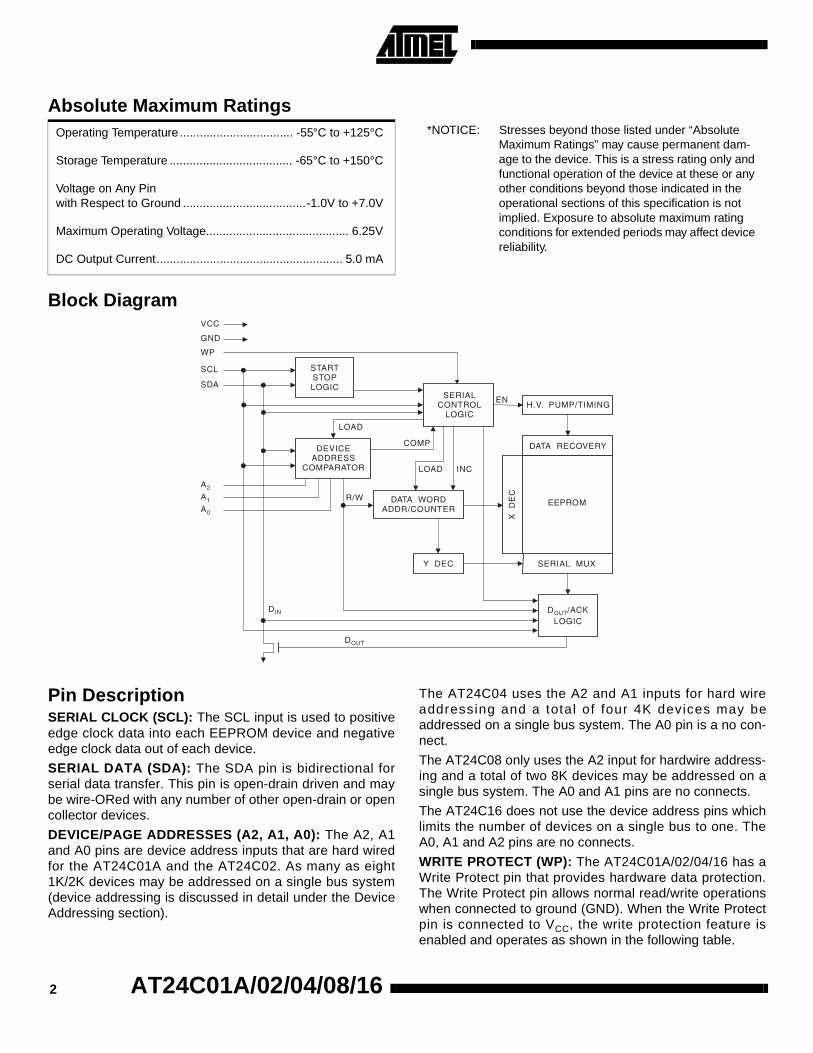
Block Diagram
Pin DescriptionSERIAL CLOCK (SCL): The SCL input is used to positiveedge clock data into each EEPROM device and negativeedge clock data out of each device.
SERIAL DATA (SDA): The SDA pin is bidirectional forserial data transfer. This pin is open-drain driven and maybe wire-ORed with any number of other open-drain or opencollector devices.
DEVICE/PAGE ADDRESSES (A2, A1, A0): The A2, A1and A0 pins are device address inputs that are hard wiredfor the AT24C01A and the AT24C02. As many as eight1K/2K devices may be addressed on a single bus system(device addressing is discussed in detail under the DeviceAddressing section).
The AT24C04 uses the A2 and A1 inputs for hard wireaddressing and a total of four 4K devices may beaddressed on a single bus system. The A0 pin is a no con-nect.
The AT24C08 only uses the A2 input for hardwire address-ing and a total of two 8K devices may be addressed on asingle bus system. The A0 and A1 pins are no connects.
The AT24C16 does not use the device address pins whichlimits the number of devices on a single bus to one. TheA0, A1 and A2 pins are no connects.
WRITE PROTECT (WP): The AT24C01A/02/04/16 has aWrite Protect pin that provides hardware data protection.The Write Protect pin allows normal read/write operationswhen connected to ground (GND). When the Write Protectpin is connected to VCC, the write protection feature isenabled and operates as shown in the following table.
Absolute Maximum RatingsOperating Temperature.................................. -55°C to +125°C *NOTICE: Stresses beyond those listed under “Absolute
Maximum Ratings” may cause permanent dam-age to the device. This is a stress rating only and functional operation of the device at these or any other conditions beyond those indicated in the operational sections of this specification is not implied. Exposure to absolute maximum rating conditions for extended periods may affect device reliability.
Storage Temperature ..................................... -65°C to +150°C
Voltage on Any Pinwith Respect to Ground .....................................-1.0V to +7.0V
Maximum Operating Voltage........................................... 6.25V
DC Output Current........................................................ 5.0 mA
AT24C01A/02/04/08/16
3
Memory OrganizationAT24C01A, 1K SERIAL EEPROM: Internally organizedwith 128 pages of 1-byte each, the 1K requires a 7-bit dataword address for random word addressing.
AT24C02, 2K SERIAL EEPROM: Internally organized with256 pages of 1-byte each, the 2K requires an 8-bit dataword address for random word addressing.
AT24C04, 4K SERIAL EEPROM: The 4K is internallyorganized with 256 pages of 2 bytes each. Random wordaddressing Chip Number requires a 9-bit data wordaddress.
AT24C08, 8K SERIAL EEPROM: The 8K is internallyorganized with 4 blocks of 256 pages of 4 bytes each. Ran-dom word addressing requires a 10-bit data word address.
AT24C16, 16K SERIAL EEPROM: The 16K is internallyorganized with 8 blocks of 256 pages of 8 bytes each. Ran-dom word addressing requires an 11-bit data wordaddress.
Note: 1. This parameter is characterized and is not 100% tested.
Note: 1. VIL min and VIH max are reference only and are not tested.
WP PinStatus
Part of the Array Protected
24C01A 24C02 24C04 24C08 24C16
At VCCFull (1K) Array
Full (2K) Array
Full (4K) Array
Normal Read/Write Operation
Upper Half(8K) Array
At GND Normal Read/Write Operations
Pin Capacitance (1)
Applicable over recommended operating range from TA = 25°C, f = 1.0 MHz, VCC = +1.8V.
DC CharacteristicsApplicable over recommended operating range from: TAI = -40°C to +85°C, VCC = +1.8V to +5.5V, TAC = 0°C to +70°C,VCC = +1.8V to +5.5V (unless otherwise noted).
Symbol Parameter Test Condition Min Typ Max Units
VCC1 Supply Voltage 1.8 5.5 V
VCC2 Supply Voltage 2.5 5.5 V
VCC3 Supply Voltage 2.7 5.5 V
VCC4 Supply Voltage 4.5 5.5 V
ICC Supply Current VCC = 5.0V READ at 100 kHz 0.4 1.0 mA
ICC Supply Current VCC = 5.0V WRITE at 100 kHz 2.0 3.0 mA
ISB1 Standby Current VCC = 1.8V VIN = VCC or VSS 0.6 3.0 µA
ISB2 Standby Current VCC = 2.5V VIN = VCC or VSS 1.4 4.0 µA
ISB3 Standby Current VCC = 2.7V VIN = VCC or VSS 1.6 4.0 µA
ISB4 Standby Current VCC = 5.0V VIN = VCC or VSS 8.0 18.0 µA
ILI Input Leakage Current VIN = VCC or VSS 0.10 3.0 µA
ILO Output Leakage Current VOUT = VCC or VSS 0.05 3.0 µA
VIL Input Low Level(1) -0.6 VCC x 0.3 V
VIH Input High Level(1) VCC x 0.7 VCC + 0.5 V
VOL2 Output Low Level VCC = 3.0V IOL = 2.1 mA 0.4 V
VOL1 Output Low Level VCC = 1.8V IOL = 0.15 mA 0.2 V
AT24C01A/02/04/08/164
Note: 1. This parameter is characterized and is not 100% tested.
Device OperationCLOCK and DATA TRANSITIONS: The SDA pin is nor-mally pulled high with an external device. Data on the SDApin may change only during SCL low time periods (refer toData Validity timing diagram). Data changes during SCLhigh periods will indicate a start or stop condition asdefined below.
START CONDITION: A high-to-low transition of SDA withSCL high is a start condition which must precede any othercommand (refer to Start and Stop Definition timing dia-gram).
STOP CONDITION: A low-to-high transition of SDA withSCL high is a stop condition. After a read sequence, thestop command will place the EEPROM in a standby powermode (refer to Start and Stop Definition timing diagram).
ACKNOWLEDGE: All addresses and data words are seri-ally transmitted to and from the EEPROM in 8-bit words.The EEPROM sends a zero to acknowledge that it hasreceived each word. This happens during the ninth clockcycle.
STANDBY MODE: The AT24C01A/02/04/08/16 features alow power standby mode which is enabled: (a) upon power-up and (b) after the receipt of the STOP bit and the comple-tion of any internal operations.
MEMORY RESET: After an interruption in protocol, powerloss or system reset, any 2-wire part can be reset by follow-ing these steps:
1. Clock up to 9 cycles.
2. Look for SDA high in each cycle while SCL is high.
3. Create a start condition as SDA is high.
AC CharacteristicsApplicable over recommended operating range from TA = -40°C to +85°C, VCC = +1.8V to +5.5V, CL = 1 TTL Gate and100pF (unless otherwise noted).
Symbol Parameter
2.7-, 2.5-, 1.8-volt 5.0-volt
UnitsMin Max Min Max
fSCL Clock Frequency, SCL 100 400 kHz
tLOW Clock Pulse Width Low 4.7 1.2 µs
tHIGH Clock Pulse Width High 4.0 0.6 µs
tI Noise Suppression Time(1) 100 50 ns
tAA Clock Low to Data Out Valid 0.1 4.5 0.1 0.9 µs
tBUFTime the bus must be free before a new transmission can start(1) 4.7 1.2 µs
tHD.STA Start Hold Time 4.0 0.6 µs
tSU.STA Start Set-up Time 4.7 0.6 µs
tHD.DAT Data In Hold Time 0 0 µs
tSU.DAT Data In Set-up Time 200 100 ns
tR Inputs Rise Time(1) 1.0 0.3 µs
tF Inputs Fall Time(1) 300 300 ns
tSU.STO Stop Set-up Time 4.7 0.6 µs
tDH Data Out Hold Time 100 50 ns
tWR Write Cycle Time 10 10 ms
Endurance(1) 5.0V, 25°C, Page Mode 1M 1MWrite
Cycles
AT24C01A/02/04/08/16
5
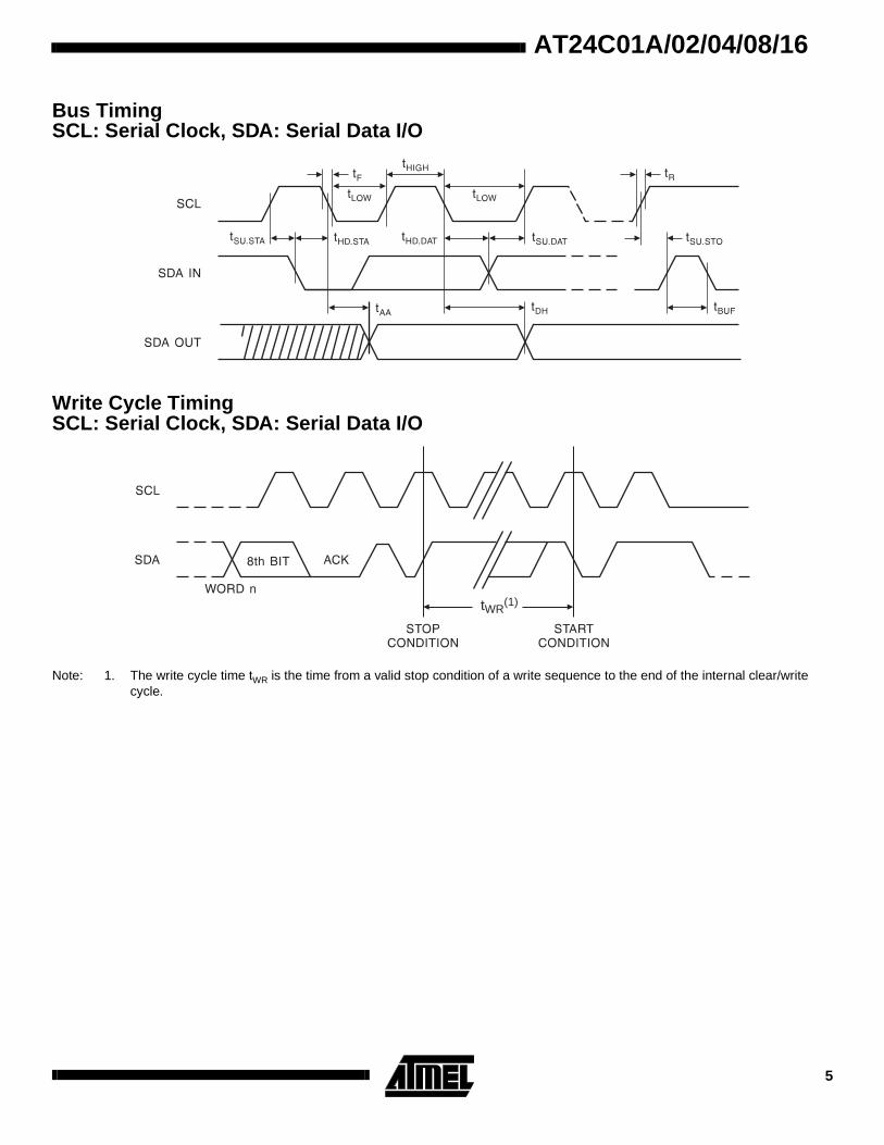
Bus TimingSCL: Serial Clock, SDA: Serial Data I/O
Write Cycle TimingSCL: Serial Clock, SDA: Serial Data I/O
Note: 1. The write cycle time tWR is the time from a valid stop condition of a write sequence to the end of the internal clear/write cycle.
tWR(1)
AT24C01A/02/04/08/166
Data Validity
Start and Stop Definition
Output Acknowledge
AT24C01A/02/04/08/16
7
Device AddressingThe 1K, 2K, 4K, 8K and 16K EEPROM devices all requirean 8-bit device address word following a start condition toenable the chip for a read or write operation (refer to Figure1).
The device address word consists of a mandatory one,zero sequence for the first four most significant bits asshown. This is common to all the EEPROM devices.
The next 3 bits are the A2, A1 and A0 device address bitsfor the 1K/2K EEPROM. These 3 bits must compare totheir corresponding hard-wired input pins.
The 4K EEPROM only uses the A2 and A1 device addressbits with the third bit being a memory page address bit. Thetwo device address bits must compare to their correspond-ing hard-wired input pins. The A0 pin is no connect.
The 8K EEPROM only uses the A2 device address bit withthe next 2 bits being for memory page addressing. The A2bit must compare to its corresponding hard-wired input pin.The A1 and A0 pins are no connect.
The 16K does not use any device address bits but insteadthe 3 bits are used for memory page addressing. Thesepage addressing bits on the 4K, 8K, and 16K devicesshould be considered the most significant bits of the dataword address which follows. The A0, A1 and A2 pins are noconnect.
The eighth bit of the device address is the read/write opera-tion select bit. A read operation is initiated if this bit is highand a write operation is initiated if this bit is low.
Upon a compare of the device address, the EEPROM willoutput a zero. If a compare is not made, the chip will returnto a standby state.
Write OperationsBYTE WRITE: A write operation requires an 8-bit dataword address following the device address word andacknowledgment. Upon receipt of this address, theEEPROM will again respond with a zero and then clock inthe first 8-bit data word. Following receipt of the 8-bit dataword, the EEPROM will output a zero and the addressingdevice, such as a microcontroller, must terminate the writesequence with a stop condition. At this time the EEPROMenters an internally-timed write cycle, tWR, to the nonvolatilememory. All inputs are disabled during this write cycle andthe EEPROM will not respond until the write is complete(refer to Figure 2).
PAGE WRITE: The 1K/2K EEPROM is capable of an 8-byte page write, and the 4K, 8K and 16K devices are capa-ble of 16-byte page writes.
A page write is initiated the same as a byte write, but themicrocontroller does not send a stop condition after the firstdata word is clocked in. Instead, after the EEPROM
acknowledges receipt of the first data word, the microcon-troller can transmit up to seven (1K/2K) or fifteen (4K, 8K,16K) more data words. The EEPROM will respond with azero after each data word received. The microcontrollermust terminate the page write sequence with a stop condi-tion (refer to Figure 3).
The data word address lower three (1K/2K) or four (4K, 8K,16K) bits are internally incremented following the receipt ofeach data word. The higher data word address bits are notincremented, retaining the memory page row location.When the word address, internally generated, reaches thepage boundary, the following byte is placed at the begin-ning of the same page. If more than eight (1K/2K) or six-teen (4K, 8K, 16K) data words are transmitted to theEEPROM, the data word address will “roll over” and previ-ous data will be overwritten.
ACKNOWLEDGE POLLING: Once the internally-timedwrite cycle has started and the EEPROM inputs are dis-abled, acknowledge polling can be initiated. This involvessending a start condition followed by the device addressword. The read/write bit is representative of the operationdesired. Only if the internal write cycle has completed willthe EEPROM respond with a zero allowing the read orwrite sequence to continue.
Read OperationsRead operations are initiated the same way as write opera-tions with the exception that the read/write select bit in thedevice address word is set to one. There are three readoperations: current address read, random address readand sequential read.
CURRENT ADDRESS READ: The internal data wordaddress counter maintains the last address accessed dur-ing the last read or write operation, incremented by one.This address stays valid between operations as long as thechip power is maintained. The address “roll over” duringread is from the last byte of the last memory page to thefirst byte of the first page. The address “roll over” duringwrite is from the last byte of the current page to the firstbyte of the same page.
Once the device address with the read/write select bit setto one is clocked in and acknowledged by the EEPROM,the current address data word is serially clocked out. Themicrocontroller does not respond with an input zero butdoes generate a following stop condition (refer to Figure 4).
RANDOM READ: A random read requires a “dummy” bytewrite sequence to load in the data word address. Once thedevice address word and data word address are clocked inand acknowledged by the EEPROM, the microcontrollermust generate another start condition. The microcontrollernow initiates a current address read by sending a deviceaddress with the read/write select bit high. The EEPROMacknowledges the device address and serially clocks out
AT24C01A/02/04/08/168
the data word. The microcontroller does not respond with azero but does generate a following stop condition (refer toFigure 5).
SEQUENTIAL READ: Sequential reads are initiated byeither a current address read or a random address read.After the microcontroller receives a data word, it respondswith an acknowledge. As long as the EEPROM receives an
acknowledge, it will continue to increment the data wordaddress and serially clock out sequential data words. Whenthe memory address limit is reached, the data wordaddress will “roll over” and the sequential read will con-tinue. The sequential read operation is terminated whenthe microcontroller does not respond with a zero but doesgenerate a following stop condition (refer to Figure 6).
Figure 1. Device Address
Figure 2. Byte Write
Figure 3. Page Write
(* = DON’T CARE bit for 1K)
AT24C01A/02/04/08/16
9
Figure 4. Current Address Read
Figure 5. Random Read
(* = DON’T CARE bit for 1K)
Figure 6. Sequential Read
AT24C01A/02/04/08/1610
AT24C01A Ordering InformationtWR (max)
(ms)ICC (max)
(µA)ISB (max)
(µA)fMAX
(kHz) Ordering Code Package Operation Range
10 3000 18 400 AT24C01A-10PCAT24C01A-10SC
AT24C01A-10MCAT24C01A-10TC
8P38S1
8M8T
Commercial(0°C to 70°C)
3000 18 400 AT24C01A-10PIAT24C01A-10SI
AT24C01A-10MIAT24C01A-10TI
8P38S1
8M8T
Industrial(-40°C to 85°C)
10 1500 4 100 AT24C01A-10PC-2.7AT24C01A-10SC-2.7
AT24C01A-10MC-2.7AT24C01A-10TC-2.7
8P38S1
8M8T
Commercial(0°C to 70°C)
1500 4 100 AT24C01A-10PI-2.7AT24C01A-10SI-2.7
AT24C01A-10MI-2.7AT24C01A-10TI-2.7
8P38S1
8M8T
Industrial(-40°C to 85°C)
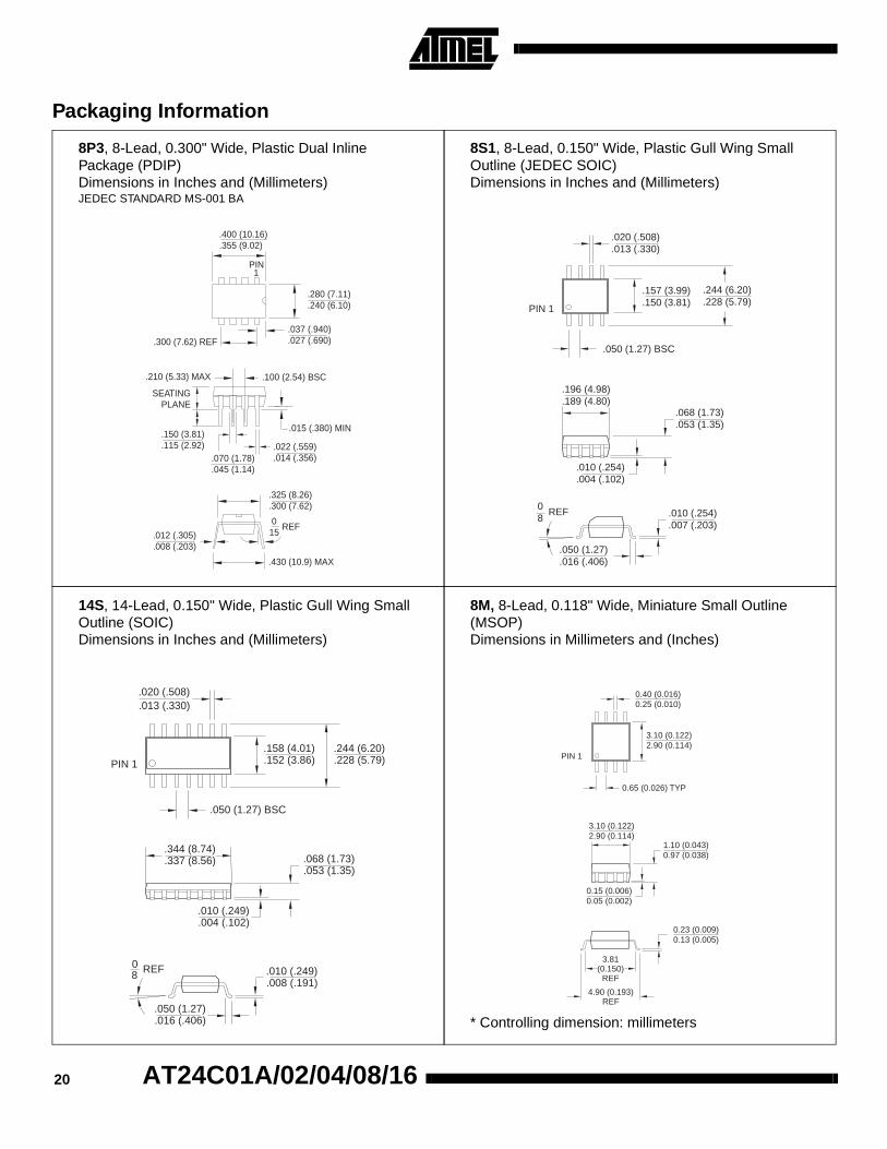
Package Type
8M 8-Lead, 0.118" Wide, Miniature Small Outline Package (MSOP)


![Study of WiMAX Based Communication Channel Effects on ...where the size of the FFT is changeable and may be equal to: 128, 512, 1024, and 2048 [13]. 2048 FFT was adopted through this](https://static.documents.pub/doc/80x56/60722ab09c1d577c547950bb/study-of-wimax-based-communication-channel-effects-on-where-the-size-of-the.jpg)


![EEDS TO CHANG - Dolby Laboratories · PDF fileEEDS TO CHANG Version 5.2 Dolby ... Society of Motion Picture & Television Engineers, ... [-1024 1024]), zlim([0 2048]), grid on; box](https://static.documents.pub/doc/80x56/5aa667517f8b9ac8748e5b2e/eeds-to-chang-dolby-laboratories-to-chang-version-52-dolby-society-of-motion.jpg)


