www.ti.com...................................................................................................................................... SLLS677A –NOVEMBER 2005–REVISED SEPTEMBER 2009
155-Mbps to 4.25-Gbps LASER DRIVERCheck for Samples: ONET4201LD
1FEATURES APPLICATIONS• SONET/SDH Transmission Systems• Multirate Operation From 155 Mbps up to 4.25
Gbps • Fibre Channel Optical Modules• Fiber Optic Data Links• Bias Current Programmable From 1 mA
to 100 mA • Digital Cross-Connects• Optical Transmitters• Modulation Current Programmable From 5 mA
to 85 mADESCRIPTION• APC and Fault Detection
• Fault Mode Selection The ONET4201LD is a laser driver for multiple fiberoptic applications up to 4.25 Gbps. The device• Bias and Photodiode Current Monitorsaccepts CML input data and provides bias and
• CML Data Inputs modulation currents for driving a laser diode. Also• Temperature Compensation of Modulation provided are automatic power control (APC),
temperature compensation of modulation current,Currentfault detection, and current monitor features.• Single 3.3-V SupplyThe device is available in a small-footprint, 4-mm ו Active Back-Termination at the Output4-mm, 24-pin, QFN package. The circuit requires a• Surface-Mount, Small-Footprint, 4-mm × 4-mm,single 3.3-V supply.24-Lead QFN PackageThis power-efficient laser driver is characterized foroperation from –40°C to 85°C.
1
Please be aware that an important notice concerning availability, standard warranty, and use in critical applications of TexasInstruments semiconductor products and disclaimers thereto appears at the end of this data sheet.
SLLS677A –NOVEMBER 2005–REVISED SEPTEMBER 2009...................................................................................................................................... www.ti.com
This integrated circuit can be damaged by ESD. Texas Instruments recommends that all integrated circuits be handled withappropriate precautions. Failure to observe proper handling and installation procedures can cause damage.
ESD damage can range from subtle performance degradation to complete device failure. Precision integrated circuits may be moresusceptible to damage because very small parametric changes could cause the device not to meet its published specifications.
DETAILED DESCRIPTION
BLOCK DIAGRAM
A simplified block diagram of the ONET4201LD is shown in Figure 1.
This compact, low-power, 4.25-Gbps laser driver circuit consists of a high-speed data path and a bias and controlblock.
The function of the data path is to buffer the input data and then modulate the laser diode current according tothe input data stream.
The bias and control block generates the laser diode bias current, contains automatic power control (APC) tomaintain constant optical output power, generates a modulation current that can be temperature compensatedand controls power-on during start-up and shutdown after failure detection. The circuit design is optimized forhigh-speed and low-voltage operation (3.3 V).
The main circuit blocks are described in detail below.
Figure 1. Simplified Block Diagram of the ONET4201LD
www.ti.com...................................................................................................................................... SLLS677A –NOVEMBER 2005–REVISED SEPTEMBER 2009
HIGH-SPEED DATA PATH
The high-speed data path consists of an input buffer stage and a current modulator.
The input buffer stage takes CML compatible differential signals. It provides on-chip 50-Ω termination to VCC.AC-coupling may be used at the DIN+ and DIN– inputs.
The laser diode current modulator mainly consists of two common-emitter output transistors and the requireddriver circuitry. Depending on the input data stream, the modulation current is sunk at the MOD+ or the MOD–pin.
Modulation current setting is performed by means of the modulation current generator block, which is supervisedby the control circuit block.
The laser diode can be either ac- or dc-coupled. In both cases, the maximum modulation current is 85 mA. Themodulation output is optimized for driving a 20-Ω load.
For optimum performance when driving a laser diode over a 20-Ω transmission line, the ONET4201LD providesactive 20-Ω back-termination, which minimizes jitter caused by reflections.
BIAS AND CONTROL
The bias and control circuitry consists of the bandgap voltage and bias generation block, the bias currentgenerator, the automatic power control block and the supervising control circuitry.
BANDGAP VOLTAGE AND BIAS GENERATION
The bandgap voltage reference provides process and temperature-independent reference voltages needed to setbias current, modulation current, and photodiode reference current. Additionally, this block provides the biasingfor all internal circuits.
AUTOMATIC POWER CONTROL
The ONET4201LD laser driver incorporates an APC loop to compensate for the changes in laser thresholdcurrent over temperature and lifetime. The internal APC is enabled when resistors are connected to the IBMAXand APCSET pins. A back-facet photodiode mounted in the laser package is used to detect the average laseroutput power. The photodiode current IPD, which is proportional to the average laser power, can be calculated byusing the laser-to-monitor transfer ratio, ρMON, and the average power, PAVG:
(1)
In closed-loop operation, the APC modifies the laser diode bias current by comparing IPD with a reference currentIAPCSET and generates a bias compensation current. IPD can be programmed by selecting the external resistorRAPCSET according to:
(2)
The bias compensation current subtracts from the maximum bias current to maintain the monitor photodiodecurrent. The maximum bias current is programmed by the resistor connected to IBMAX:
(3)
This current limit establishes the maximum bias current available in closed loop mode, as well as in transientfault conditions such as shorts at the PD pin to ground or delayed laser power up.
An external pin MONB is provided as a bias current monitor output. A fraction of the bias current (1/68) ismirrored and develops a voltage drop across an external resistor to ground, RMONB. The voltage at MONB isgiven as:
(4)
If the voltage at MONB is greater than the programmed threshold, a fault mode occurs.
SLLS677A –NOVEMBER 2005–REVISED SEPTEMBER 2009...................................................................................................................................... www.ti.com
The MONP is also provided as a photocurrent monitor output. The photodiode current, IPD, is mirrored anddevelops a voltage across an external resistor to ground, RMONP. The voltage at MONP is given as:
(5)
If the voltage at MONP is greater than the programmed threshold, a fault mode occurs.
As with any negative-feedback system design, care must be taken to assure stability of the loop. The loopbandwidth must not be too high in order to minimize pattern-dependent jitter. The dominant pole is determined bythe capacitor CAPC. The recommended value for CAPC is 200 nF. The capacitance of the monitor photodiode CPDadds another pole to the system, and thus it must be small enough to maintain stability. The recommended valuefor this capacitance is CPD ≤ 50 pF.
The internal APC loop can be disabled by connecting a 100-kΩ resistor from APCSET to VCC and leaving PDopen. In open-loop operation, the laser diode current is set by IBIASMAX and IMODSET.
MODULATION-CURRENT GENERATOR
The modulation-current generator defines the tail current of the modulator, which is sunk from either MOD+ orMOD–, depending on the data pattern. The modulation current consists of a modulation current IMOD0 at areference temperature T0 = 60°C (set by the resistor RMODSET) and a temperature-dependent modulation currentdefined by the resistor RMODTC. The modulation current can be estimated as follows:
(6)
Note that the reference temperature, T0, and the temperature compensation set by RMODTC vary from part to part.To reduce the variation, IMOD can be calibrated over temperature and set with a microcontroller DAC or digitalpotentiometer.
CONTROL
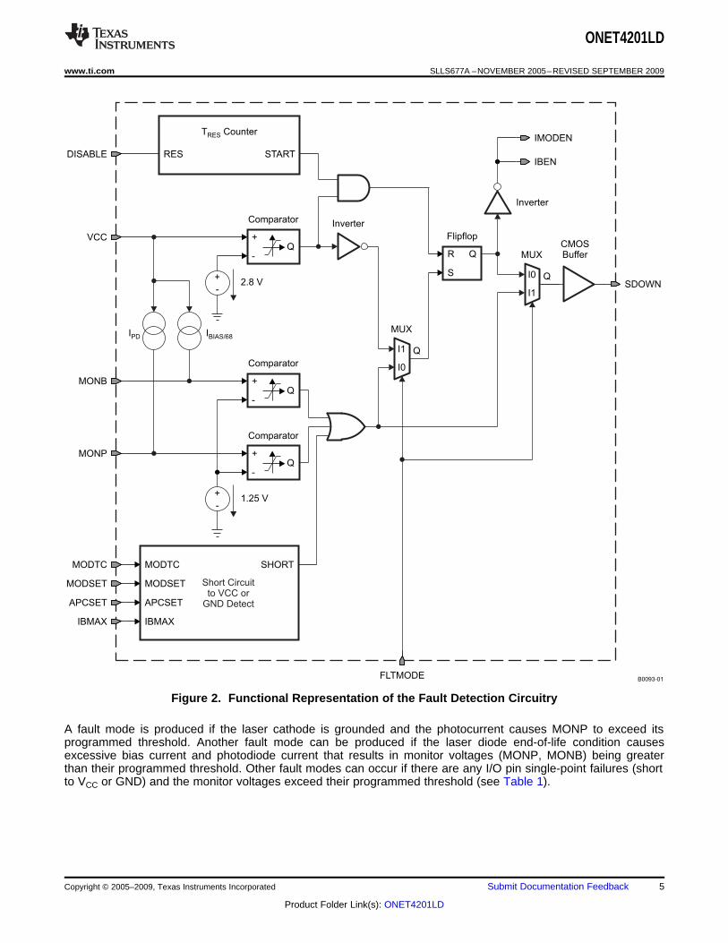
The functions of this block are to control the start-up sequence, detect faults, detect tracking failure of the APCloop, and provide disable control. The laser driver has a controlled start-up sequence, which helps preventtransient glitches from being applied to the laser during power on. At start-up, the laser diode is off, SDOWN islow, and the APC loop is open. Once VCC reaches ~2.8 V, the laser diode bias generator and modulation currentgenerator circuitry are activated (if DISABLE is low). The slow-start circuitry gradually brings up the currentdelivered to the laser diode. From the time that VCC reaches ~2.8 V until the modulation current and bias currentreach 95% of their steady state value, is considered the initialization time. If DISABLE is asserted during poweron, the slow-start circuitry does not activate until DISABLE is negated.
FAULT DETECTION
The fault-detection circuitry monitors the operation of the ONET4201LD. If FLTMODE is set to a low level,(hard-fault mode) this circuitry disables the bias and modulation circuits and latches the SDOWN output ondetection of a fault. The fault mode is reset by toggling DISABLE (for a minimum time of TRES) or by toggling VCC.
Once DISABLE is toggled, SDOWN is set low and the circuit is re-initialized.
If FLTMODE is set to a high level (soft-fault mode), a fault is indicated at the SDOWN output; however, the biasand modulation circuits are not disabled. The SDOWN output is reset once the fault causing conditiondisappears. Toggling DISABLE or VCC is not required.
A functional representation of the fault detection circuitry is shown in Figure 2.
www.ti.com...................................................................................................................................... SLLS677A –NOVEMBER 2005–REVISED SEPTEMBER 2009
Figure 2. Functional Representation of the Fault Detection Circuitry
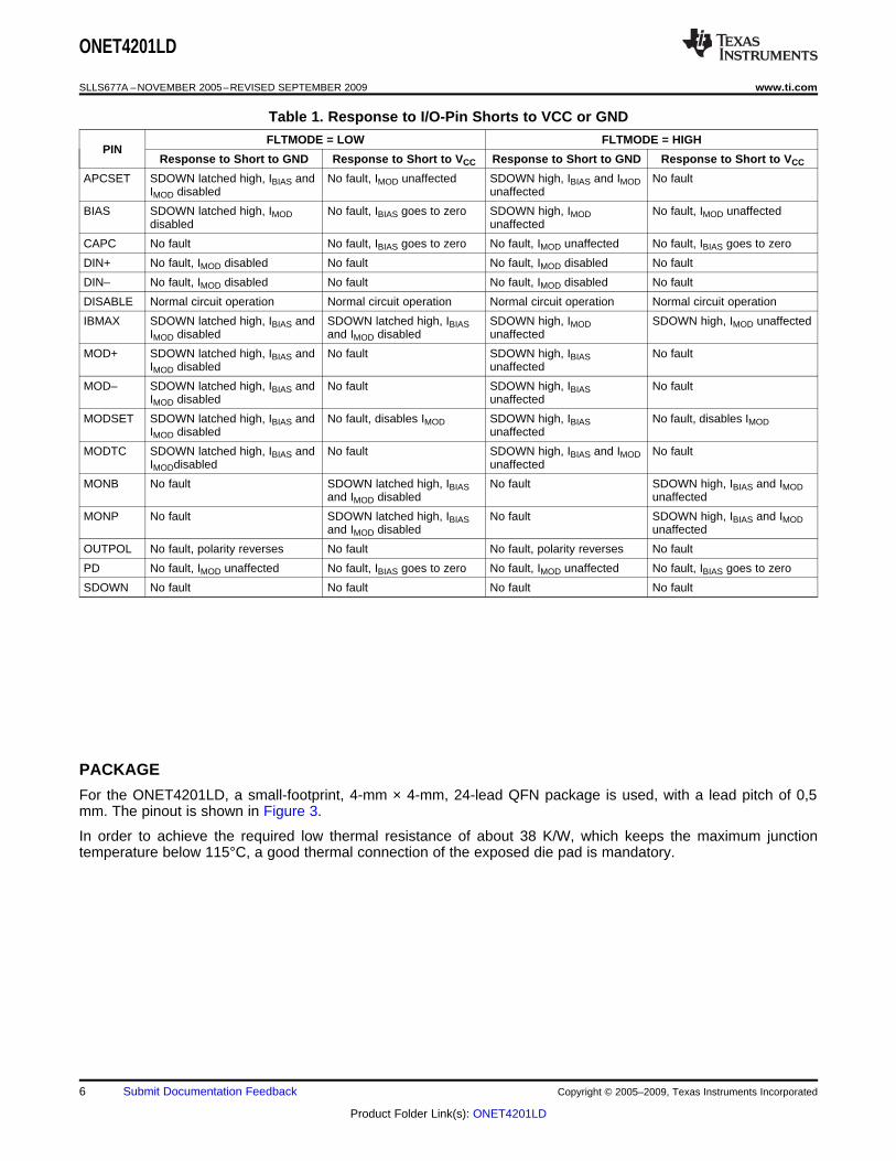
A fault mode is produced if the laser cathode is grounded and the photocurrent causes MONP to exceed itsprogrammed threshold. Another fault mode can be produced if the laser diode end-of-life condition causesexcessive bias current and photodiode current that results in monitor voltages (MONP, MONB) being greaterthan their programmed threshold. Other fault modes can occur if there are any I/O pin single-point failures (shortto VCC or GND) and the monitor voltages exceed their programmed threshold (see Table 1).
SLLS677A –NOVEMBER 2005–REVISED SEPTEMBER 2009...................................................................................................................................... www.ti.com
Table 1. Response to I/O-Pin Shorts to VCC or GND
FLTMODE = LOW FLTMODE = HIGHPIN
Response to Short to GND Response to Short to VCC Response to Short to GND Response to Short to VCC
APCSET SDOWN latched high, IBIAS and No fault, IMOD unaffected SDOWN high, IBIAS and IMOD No faultIMOD disabled unaffected
BIAS SDOWN latched high, IMOD No fault, IBIAS goes to zero SDOWN high, IMOD No fault, IMOD unaffecteddisabled unaffected
CAPC No fault No fault, IBIAS goes to zero No fault, IMOD unaffected No fault, IBIAS goes to zero
DIN+ No fault, IMOD disabled No fault No fault, IMOD disabled No fault
DIN– No fault, IMOD disabled No fault No fault, IMOD disabled No fault
DISABLE Normal circuit operation Normal circuit operation Normal circuit operation Normal circuit operation
IBMAX SDOWN latched high, IBIAS and SDOWN latched high, IBIAS SDOWN high, IMOD SDOWN high, IMOD unaffectedIMOD disabled and IMOD disabled unaffected
MOD+ SDOWN latched high, IBIAS and No fault SDOWN high, IBIAS No faultIMOD disabled unaffected
MOD– SDOWN latched high, IBIAS and No fault SDOWN high, IBIAS No faultIMOD disabled unaffected
MODSET SDOWN latched high, IBIAS and No fault, disables IMOD SDOWN high, IBIAS No fault, disables IMODIMOD disabled unaffected
MODTC SDOWN latched high, IBIAS and No fault SDOWN high, IBIAS and IMOD No faultIMODdisabled unaffected
MONB No fault SDOWN latched high, IBIAS No fault SDOWN high, IBIAS and IMODand IMOD disabled unaffected
MONP No fault SDOWN latched high, IBIAS No fault SDOWN high, IBIAS and IMODand IMOD disabled unaffected
OUTPOL No fault, polarity reverses No fault No fault, polarity reverses No fault
PD No fault, IMOD unaffected No fault, IBIAS goes to zero No fault, IMOD unaffected No fault, IBIAS goes to zero
SDOWN No fault No fault No fault No fault
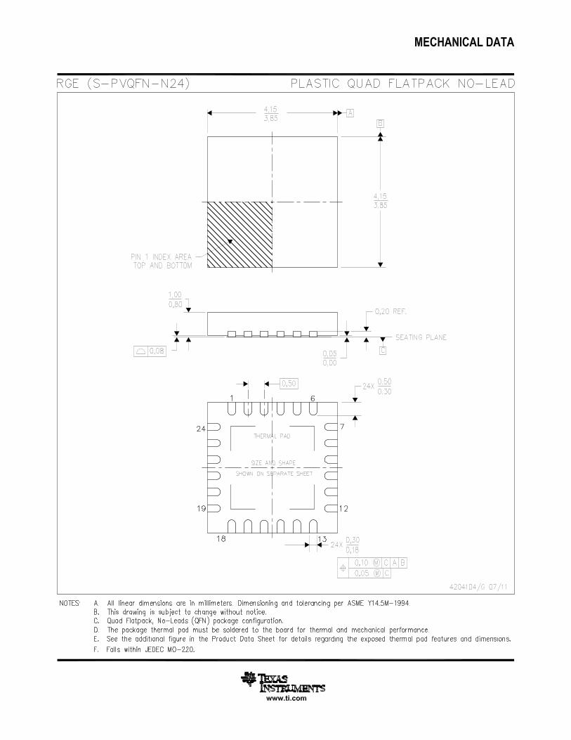
PACKAGE
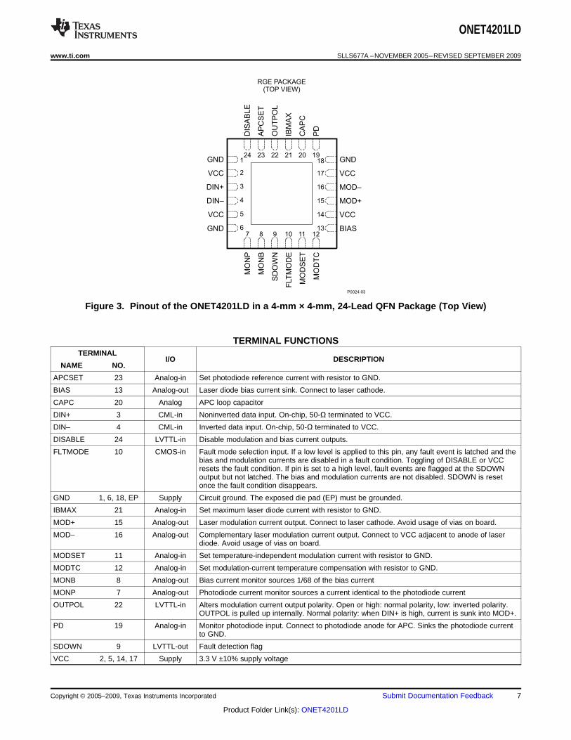
For the ONET4201LD, a small-footprint, 4-mm × 4-mm, 24-lead QFN package is used, with a lead pitch of 0,5mm. The pinout is shown in Figure 3.
In order to achieve the required low thermal resistance of about 38 K/W, which keeps the maximum junctiontemperature below 115°C, a good thermal connection of the exposed die pad is mandatory.
www.ti.com...................................................................................................................................... SLLS677A –NOVEMBER 2005–REVISED SEPTEMBER 2009
Figure 3. Pinout of the ONET4201LD in a 4-mm × 4-mm, 24-Lead QFN Package (Top View)
TERMINAL FUNCTIONSTERMINAL
I/O DESCRIPTIONNAME NO.
APCSET 23 Analog-in Set photodiode reference current with resistor to GND.
BIAS 13 Analog-out Laser diode bias current sink. Connect to laser cathode.
CAPC 20 Analog APC loop capacitor
DIN+ 3 CML-in Noninverted data input. On-chip, 50-Ω terminated to VCC.
DIN– 4 CML-in Inverted data input. On-chip, 50-Ω terminated to VCC.
DISABLE 24 LVTTL-in Disable modulation and bias current outputs.
FLTMODE 10 CMOS-in Fault mode selection input. If a low level is applied to this pin, any fault event is latched and thebias and modulation currents are disabled in a fault condition. Toggling of DISABLE or VCCresets the fault condition. If pin is set to a high level, fault events are flagged at the SDOWNoutput but not latched. The bias and modulation currents are not disabled. SDOWN is resetonce the fault condition disappears.
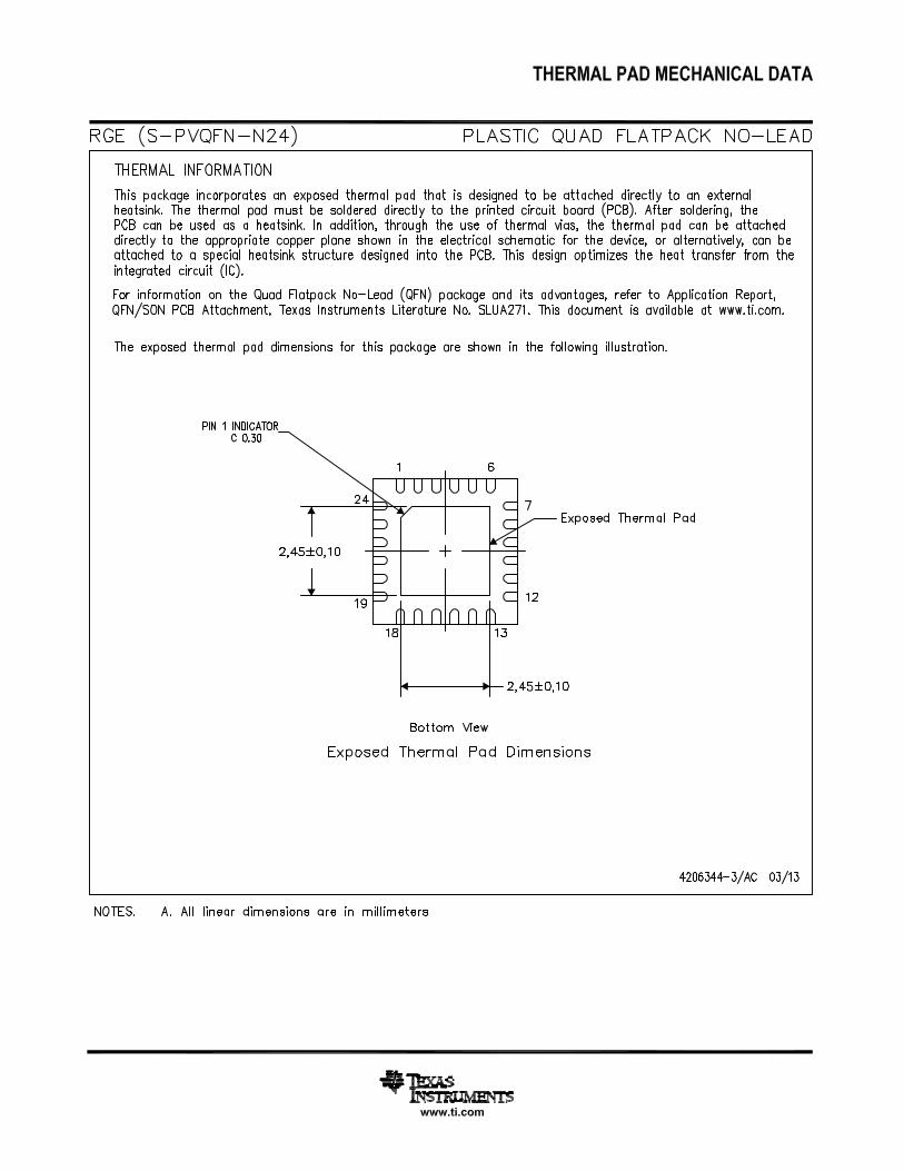
GND 1, 6, 18, EP Supply Circuit ground. The exposed die pad (EP) must be grounded.
IBMAX 21 Analog-in Set maximum laser diode current with resistor to GND.
MOD+ 15 Analog-out Laser modulation current output. Connect to laser cathode. Avoid usage of vias on board.
MOD– 16 Analog-out Complementary laser modulation current output. Connect to VCC adjacent to anode of laserdiode. Avoid usage of vias on board.
MODSET 11 Analog-in Set temperature-independent modulation current with resistor to GND.
MODTC 12 Analog-in Set modulation-current temperature compensation with resistor to GND.
MONB 8 Analog-out Bias current monitor sources 1/68 of the bias current
MONP 7 Analog-out Photodiode current monitor sources a current identical to the photodiode current
OUTPOL 22 LVTTL-in Alters modulation current output polarity. Open or high: normal polarity, low: inverted polarity.OUTPOL is pulled up internally. Normal polarity: when DIN+ is high, current is sunk into MOD+.
PD 19 Analog-in Monitor photodiode input. Connect to photodiode anode for APC. Sinks the photodiode currentto GND.
SLLS677A –NOVEMBER 2005–REVISED SEPTEMBER 2009...................................................................................................................................... www.ti.com
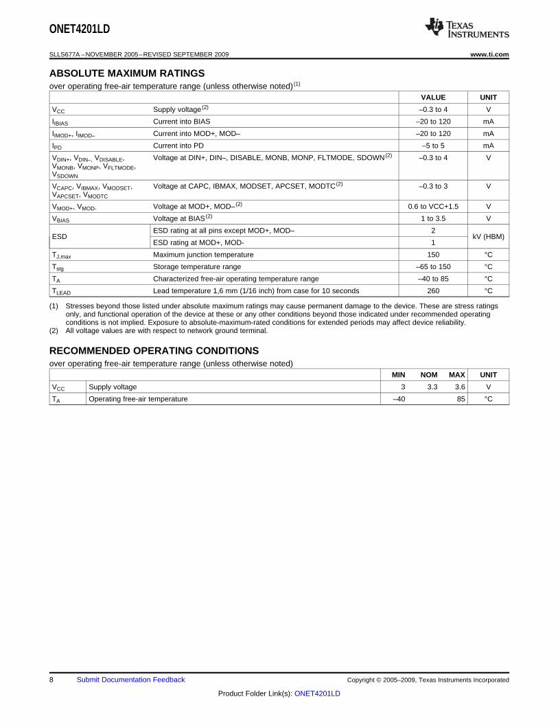
ABSOLUTE MAXIMUM RATINGSover operating free-air temperature range (unless otherwise noted) (1)
VALUE UNIT
VCC Supply voltage (2) –0.3 to 4 V
IIBIAS Current into BIAS –20 to 120 mA
IIMOD+, IIMOD– Current into MOD+, MOD– –20 to 120 mA
IPD Current into PD –5 to 5 mA
VDIN+, VDIN–, VDISABLE, Voltage at DIN+, DIN–, DISABLE, MONB, MONP, FLTMODE, SDOWN (2) –0.3 to 4 VVMONB, VMONP, VFLTMODE,VSDOWN
VCAPC, VIBMAX, VMODSET, Voltage at CAPC, IBMAX, MODSET, APCSET, MODTC (2) –0.3 to 3 VVAPCSET, VMODTC
VMOD+, VMOD- Voltage at MOD+, MOD– (2) 0.6 to VCC+1.5 V
VBIAS Voltage at BIAS (2) 1 to 3.5 V
ESD rating at all pins except MOD+, MOD– 2ESD kV (HBM)
ESD rating at MOD+, MOD- 1
TJ,max Maximum junction temperature 150 °C
Tstg Storage temperature range –65 to 150 °C
TA Characterized free-air operating temperature range –40 to 85 °C
TLEAD Lead temperature 1,6 mm (1/16 inch) from case for 10 seconds 260 °C
(1) Stresses beyond those listed under absolute maximum ratings may cause permanent damage to the device. These are stress ratingsonly, and functional operation of the device at these or any other conditions beyond those indicated under recommended operatingconditions is not implied. Exposure to absolute-maximum-rated conditions for extended periods may affect device reliability.
(2) All voltage values are with respect to network ground terminal.
RECOMMENDED OPERATING CONDITIONSover operating free-air temperature range (unless otherwise noted)
SLLS677A –NOVEMBER 2005–REVISED SEPTEMBER 2009...................................................................................................................................... www.ti.com
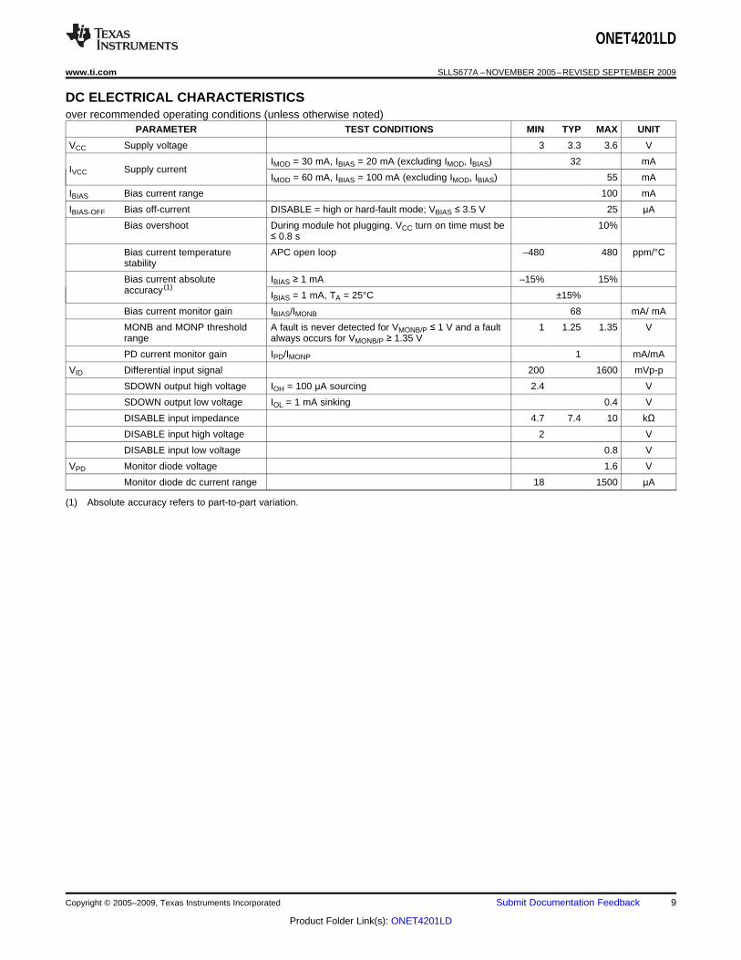
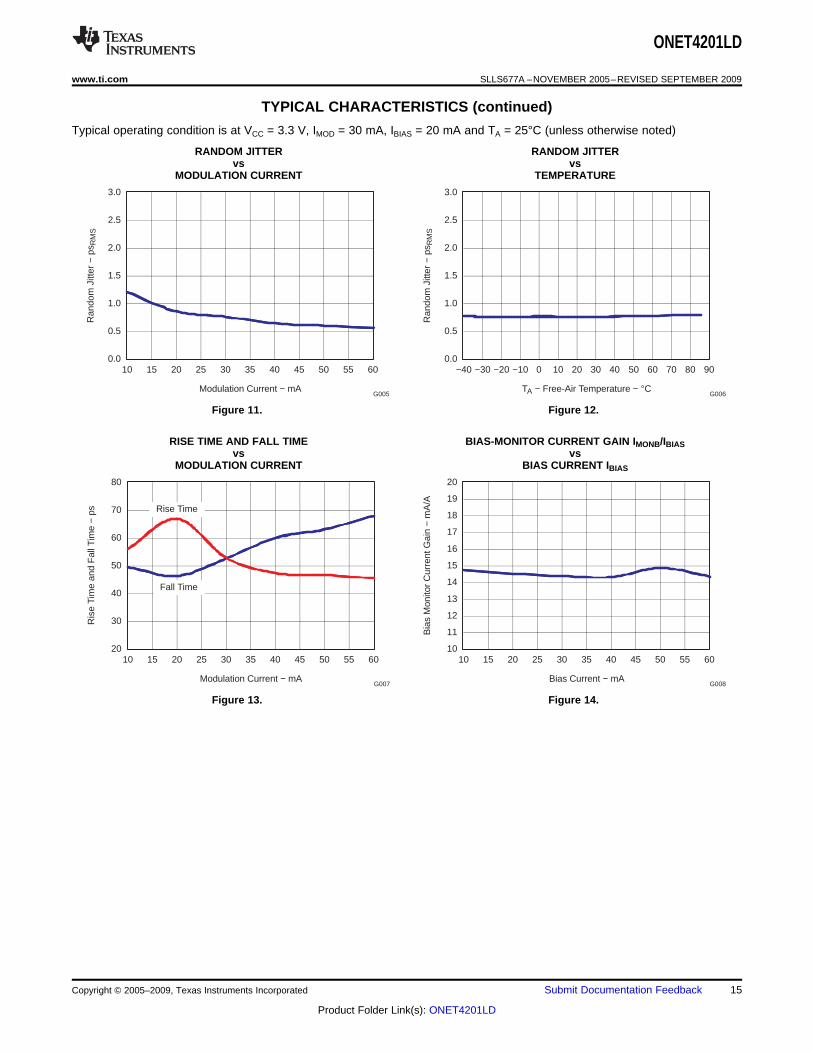
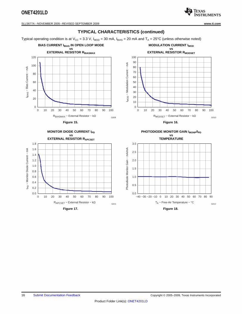
AC ELECTRICAL CHARACTERISTICSTypical operating condition is at VCC = 3.3 V, IMOD = 30 mA, IBIAS = 20 mA and TA = 25°C,over recommended operating conditions (unless otherwise noted)
PARAMETER TEST CONDITIONS MIN TYP MAX UNIT
Data Rate 4.25 Gbps
IMOD Modulation current range Current into MOD+/MOD– pin; 5 85 mAVMOD+, VMOD– ≥ 0.6 V
IMOD-OFF Modulation off-current DISABLE = high or hard-fault occurred 25 μA
Modulation current stability –600 600 ppm/°C
IMOD = 10 mA ±40%Modulation current absolute IMOD = 50 mA ±25%accuracy (1)
IMOD = 80 mA ±20%
RMODTC = 3.125 kΩ 8300Modulation current ppm/°Ctemperature compensation (2)RMODTC = Open 630
tr Output rise time (20% to 80%) VMOD+ ≥ 1 V, VMOD– ≥ 1 V, IMOD = 30 mA 55 75 ps
tf Output fall time (20% to 80%) VMOD+ ≥ 1 V, VMOD– ≥ 1 V, IMOD = 30 mA 55 75 ps
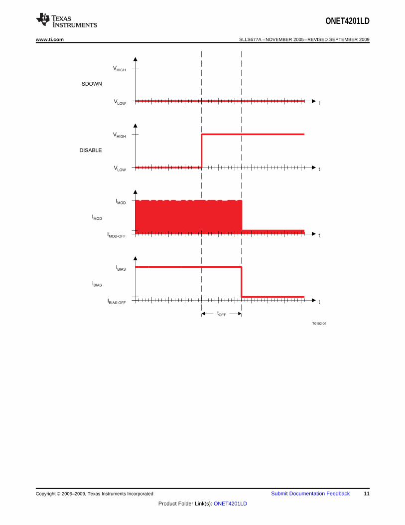
tOFF Disable assert time (see Figure 4) Time from rising edge of DISABLE to when output 0.06 5 μscurrents fall below the maximum limits of IMOD-OFFand IBIAS-OFF
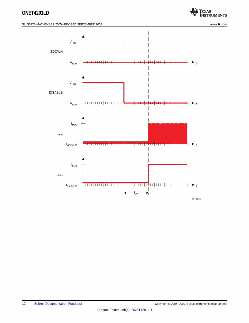
tON Disable negate time (see Figure 5) Time from falling edge of DISABLE to when output is 80 μs90% of nominal
tINIT Time to initialize From power on or negation of SDOWN using 80 μsDISABLE
tFAULT Fault assert time Time from fault to SDOWN rising edge 3.3 50 μs
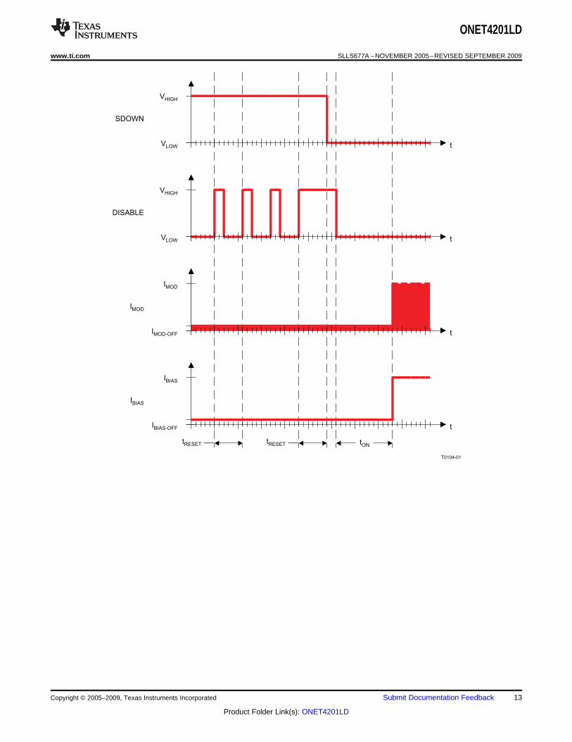
Maximum spike pulse length at DISABLE being 0.8 μsignoredtRESET DISABLE reset (see Figure 6)Time DISABLE must be high to reset SDOWN 6 μs
Output overshoot/undershoot –13.5% 13.5%
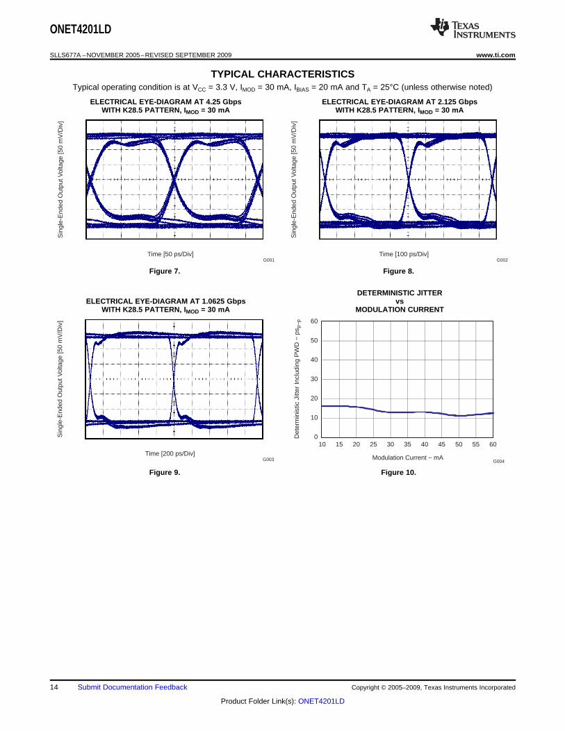
Random jitter IMOD = 60 mA 0.6 0.9 psRMS
10 mA ≤ IMOD ≤ 60 mA, with K28.5 pattern 15 30 psp-pat 4.25 Gbps
10 mA ≤ IMOD ≤ 60 mA, with 223 – 1 PRBS or 13 32 psp-pDJ Deterministic jitter (3)
equivalent pattern at 2.67 Gbps
K28.5 pattern at 1.06 Gbps 5 psp-p
223 – 1 PRBS or equivalent pattern at 155 Mbps 10 psp-p
(1) Absolute accuracy refers to part-to-part variation.(2) For a given external resistor connected to the MODTC pin, the modulation current temperature compensation will vary due to
part-to-part variations.(3) Jitter measured at positive edge and negative edge crossing of eye diagram.
SLLS677A –NOVEMBER 2005–REVISED SEPTEMBER 2009...................................................................................................................................... www.ti.com
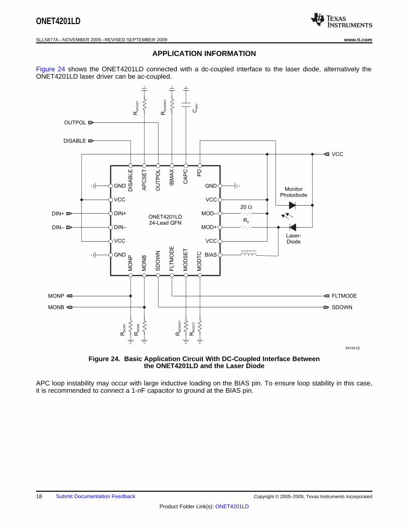
APPLICATION INFORMATION
Figure 24 shows the ONET4201LD connected with a dc-coupled interface to the laser diode, alternatively theONET4201LD laser driver can be ac-coupled.
Figure 24. Basic Application Circuit With DC-Coupled Interface Betweenthe ONET4201LD and the Laser Diode
APC loop instability may occur with large inductive loading on the BIAS pin. To ensure loop stability in this case,it is recommended to connect a 1-nF capacitor to ground at the BIAS pin.
www.ti.com...................................................................................................................................... SLLS677A –NOVEMBER 2005–REVISED SEPTEMBER 2009
SELECT A LASER
In the design example according to Figure 24, the ONET4201LD is dc coupled to a typical communication-gradelaser diode capable of operating at 4.25 Gbps with the specifications shown in Table 2.
Table 2. Laser Diode Specifications
PARAMETER VALUE UNITS
λ Wavelength 1310 nm
PAVG Average optical output power 5 mW
ITH Threshold current 10 mA
ρMON Laser-to-monitor transfer 0.05 mA/mW
η Laser slope efficiency 0.2 mW/mA
SELECT APCSET RESISTOR
When the APC loop is activated, the desired average optical output power PAVG is defined by characteristics ofthe monitor diode and by the APCSET resistor RAPCSET. The relation between the monitor photodiode current IPDand the average optical output power PAVG is given by Equation 7:
(7)
The RAPCSET resistor is calculated by Equation 8:
(8)
For the laser diode specified in Table 2 and the desired average optical output power of 5 mW, RAPCSET iscalculated as seen in Equation 9:
(9)
Note that the monitor photodiode current IPD must not exceed 1.5 mA corresponding to a minimum APCSETresistor RAPCSET,MIN = 3.1 kΩ.
SELECT MODSET RESISTOR
Modulation current IMOD is dependent on the required optical output peak-to-peak power Pp-p or the averageoptical power PAVG. IMOD can be calculated using the laser slope efficiency η and the desired extinction ratio re:
(10)
Using the laser diode parameters from Table 2 and assuming an extinction ratio re = 8 dB ( 6.3) for an averageoptical power PAVG = 5 mW the required modulation current results as:
(11)
The modulation current is adjustable with a selectable temperature coefficient TC according to the relation:
(12)
where T is the ambient temperature in °C and T0 is the reference temperature (T0 = 60°C).
The temperature coefficient of the modulation current TC is typically adjustable between 630 ppm/°C and 8300ppm/°C.
For calculation of the required external resistor RMODSET for a given modulation current and a given temperature,the formula can be modified as follows:
SLLS677A –NOVEMBER 2005–REVISED SEPTEMBER 2009...................................................................................................................................... www.ti.com
(13)
If 4000 ppm/°C is the desired temperature coefficient and the modulation current from the example above,36.3 mA, is required at a temperature of 25°C, the MODSET resistor RMODSET is given by Equation 14.
(14)
Note that the modulation current IMOD must not exceed 85 mA over the complete temperature range,corresponding to a minimum MODSET resistor RMODSET,MIN = 3.1 kΩ.
SELECT MODTC RESISTOR
The RMODTC resistor is used to program a modulation temperature coefficient that can be used to compensate forthe decreased slope efficiency of the laser at a higher temperature. The temperature coefficient TCLD of the lasercan be calculated using the slope efficiency η1 at temperature T1 and η2 at temperature T2 as shown inEquation 15:
(15)
As an example, for the laser in Table 2, the slope efficiency at temperature T1 = 25°C is η1 = 0.2 mW/mA. Attemperature T2 = 85°C the slope efficiency is η2 = 0.15 mW/mA. The corresponding temperature coefficient TCLDlaser can be calculated:
(16)
The MODTC resistor RMODTC can be used to compensate the laser temperature coefficient TCLD in order tomaintain the same optical output swing within a range of 630 ppm up to 8300 ppm. For this, RMODTC may beprogrammed as follows:
(17)
To compensate for the decreased slope efficiency of the laser in Table 2, TC must be 4167 ppm/°C.
This leads to the following MODTC resistor RMODTC:
(18)
SELECT BIASMAX RESISTOR
The BIASMAX resistor RBIASMAX is used to limit the bias current applied to the laser diode.
To calculate RBIASMAX, the maximum threshold current at 85°C and end of life must be determined. Themaximum bias current for the dc-coupled interface can be approximated by Equation 19.
www.ti.com...................................................................................................................................... SLLS677A –NOVEMBER 2005–REVISED SEPTEMBER 2009
(20)
For the example laser diode, the maximum threshold current is 40 mA at 85°C. Therefore, RBIASMAX can beapproximated by Equation 21.
(21)
SELECT VMONB AND VMONP RANGE
Monitoring the bias current is achieved by taking the fractional (1/68) bias current and developing a voltageacross an external resistor to ground. Equation 22 provides the value for VMONB for a resistor value equal to768 Ω.
(22)
Monitoring of the photodiode current is achieved by taking a mirror of IPD and developing a voltage across anexternal resistor to ground. Equation 23 provides the value for VMONP for a resistor equal to 200 Ω.
(23)
LASER DIODE INTERFACE
The output stage of the ONET4201LD is optimized for driving a 20-Ω load. The combination of a dampingresistor, RD, along with the resistance of the laser diode must be 20 Ω for impedance matching. The suggestedtypical value for RD is 6 Ω to 15 Ω. A bypass capacitor of 10 nF placed close to the laser anode also helps tooptimize performance.
SLLS677A –NOVEMBER 2005–REVISED SEPTEMBER 2009...................................................................................................................................... www.ti.com
REVISION HISTORY
Changes from Original (November 2005) to Revision A ................................................................................................ Page
• Changed 200us to 80us for typ value of tON ....................................................................................................................... 10
• Changed 200us to 80us for typ value of tINIT ...................................................................................................................... 10
• Changed 10us to 0.8us for max value of tRESET max spike ................................................................................................. 10
• Changed 20us min to 6us max value of tRESET time DISABLE ........................................................................................... 10
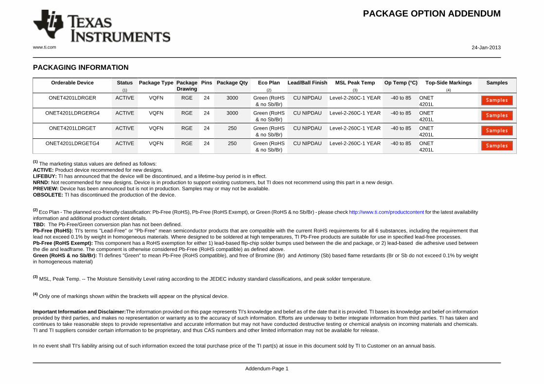
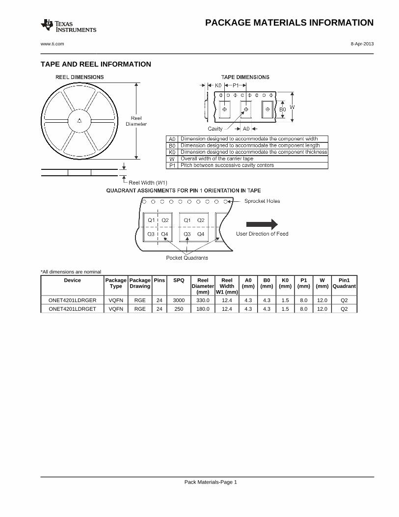
ONET4201LDRGER ACTIVE VQFN RGE 24 3000 Green (RoHS& no Sb/Br)
CU NIPDAU Level-2-260C-1 YEAR -40 to 85 ONET4201L
ONET4201LDRGERG4 ACTIVE VQFN RGE 24 3000 Green (RoHS& no Sb/Br)
CU NIPDAU Level-2-260C-1 YEAR -40 to 85 ONET4201L
ONET4201LDRGET ACTIVE VQFN RGE 24 250 Green (RoHS& no Sb/Br)
CU NIPDAU Level-2-260C-1 YEAR -40 to 85 ONET4201L
ONET4201LDRGETG4 ACTIVE VQFN RGE 24 250 Green (RoHS& no Sb/Br)
CU NIPDAU Level-2-260C-1 YEAR -40 to 85 ONET4201L
(1) The marketing status values are defined as follows:ACTIVE: Product device recommended for new designs.LIFEBUY: TI has announced that the device will be discontinued, and a lifetime-buy period is in effect.NRND: Not recommended for new designs. Device is in production to support existing customers, but TI does not recommend using this part in a new design.PREVIEW: Device has been announced but is not in production. Samples may or may not be available.OBSOLETE: TI has discontinued the production of the device.
(2) Eco Plan - The planned eco-friendly classification: Pb-Free (RoHS), Pb-Free (RoHS Exempt), or Green (RoHS & no Sb/Br) - please check http://www.ti.com/productcontent for the latest availabilityinformation and additional product content details.TBD: The Pb-Free/Green conversion plan has not been defined.Pb-Free (RoHS): TI's terms "Lead-Free" or "Pb-Free" mean semiconductor products that are compatible with the current RoHS requirements for all 6 substances, including the requirement thatlead not exceed 0.1% by weight in homogeneous materials. Where designed to be soldered at high temperatures, TI Pb-Free products are suitable for use in specified lead-free processes.Pb-Free (RoHS Exempt): This component has a RoHS exemption for either 1) lead-based flip-chip solder bumps used between the die and package, or 2) lead-based die adhesive used betweenthe die and leadframe. The component is otherwise considered Pb-Free (RoHS compatible) as defined above.Green (RoHS & no Sb/Br): TI defines "Green" to mean Pb-Free (RoHS compatible), and free of Bromine (Br) and Antimony (Sb) based flame retardants (Br or Sb do not exceed 0.1% by weightin homogeneous material)
(3) MSL, Peak Temp. -- The Moisture Sensitivity Level rating according to the JEDEC industry standard classifications, and peak solder temperature.
(4) Only one of markings shown within the brackets will appear on the physical device.
Important Information and Disclaimer:The information provided on this page represents TI's knowledge and belief as of the date that it is provided. TI bases its knowledge and belief on informationprovided by third parties, and makes no representation or warranty as to the accuracy of such information. Efforts are underway to better integrate information from third parties. TI has taken andcontinues to take reasonable steps to provide representative and accurate information but may not have conducted destructive testing or chemical analysis on incoming materials and chemicals.TI and TI suppliers consider certain information to be proprietary, and thus CAS numbers and other limited information may not be available for release.
In no event shall TI's liability arising out of such information exceed the total purchase price of the TI part(s) at issue in this document sold by TI to Customer on an annual basis.
Texas Instruments Incorporated and its subsidiaries (TI) reserve the right to make corrections, enhancements, improvements and otherchanges to its semiconductor products and services per JESD46, latest issue, and to discontinue any product or service per JESD48, latestissue. Buyers should obtain the latest relevant information before placing orders and should verify that such information is current andcomplete. All semiconductor products (also referred to herein as “components”) are sold subject to TI’s terms and conditions of salesupplied at the time of order acknowledgment.
TI warrants performance of its components to the specifications applicable at the time of sale, in accordance with the warranty in TI’s termsand conditions of sale of semiconductor products. Testing and other quality control techniques are used to the extent TI deems necessaryto support this warranty. Except where mandated by applicable law, testing of all parameters of each component is not necessarilyperformed.
TI assumes no liability for applications assistance or the design of Buyers’ products. Buyers are responsible for their products andapplications using TI components. To minimize the risks associated with Buyers’ products and applications, Buyers should provideadequate design and operating safeguards.
TI does not warrant or represent that any license, either express or implied, is granted under any patent right, copyright, mask work right, orother intellectual property right relating to any combination, machine, or process in which TI components or services are used. Informationpublished by TI regarding third-party products or services does not constitute a license to use such products or services or a warranty orendorsement thereof. Use of such information may require a license from a third party under the patents or other intellectual property of thethird party, or a license from TI under the patents or other intellectual property of TI.
Reproduction of significant portions of TI information in TI data books or data sheets is permissible only if reproduction is without alterationand is accompanied by all associated warranties, conditions, limitations, and notices. TI is not responsible or liable for such altereddocumentation. Information of third parties may be subject to additional restrictions.
Resale of TI components or services with statements different from or beyond the parameters stated by TI for that component or servicevoids all express and any implied warranties for the associated TI component or service and is an unfair and deceptive business practice.TI is not responsible or liable for any such statements.
Buyer acknowledges and agrees that it is solely responsible for compliance with all legal, regulatory and safety-related requirementsconcerning its products, and any use of TI components in its applications, notwithstanding any applications-related information or supportthat may be provided by TI. Buyer represents and agrees that it has all the necessary expertise to create and implement safeguards whichanticipate dangerous consequences of failures, monitor failures and their consequences, lessen the likelihood of failures that might causeharm and take appropriate remedial actions. Buyer will fully indemnify TI and its representatives against any damages arising out of the useof any TI components in safety-critical applications.
In some cases, TI components may be promoted specifically to facilitate safety-related applications. With such components, TI’s goal is tohelp enable customers to design and create their own end-product solutions that meet applicable functional safety standards andrequirements. Nonetheless, such components are subject to these terms.
No TI components are authorized for use in FDA Class III (or similar life-critical medical equipment) unless authorized officers of the partieshave executed a special agreement specifically governing such use.
Only those TI components which TI has specifically designated as military grade or “enhanced plastic” are designed and intended for use inmilitary/aerospace applications or environments. Buyer acknowledges and agrees that any military or aerospace use of TI componentswhich have not been so designated is solely at the Buyer's risk, and that Buyer is solely responsible for compliance with all legal andregulatory requirements in connection with such use.
TI has specifically designated certain components as meeting ISO/TS16949 requirements, mainly for automotive use. In any case of use ofnon-designated products, TI will not be responsible for any failure to meet ISO/TS16949.
Products Applications
Audio www.ti.com/audio Automotive and Transportation www.ti.com/automotive
Amplifiers amplifier.ti.com Communications and Telecom www.ti.com/communications
Data Converters dataconverter.ti.com Computers and Peripherals www.ti.com/computers


![Untitled-2 [fogokitchen.com] · BEERS e CIDER 1 Pint £5.95 £5.95 £4.25 £4.25 £4.25 £7.95 Coke Ginger Ale Slim Line Tonic SOFT DRINKS £2.95 £2.45 £3.55 £3.25 £4.25](https://static.documents.pub/doc/80x56/5fb7f6f1f5eb5306ef5358d3/untitled-2-beers-e-cider-1-pint-595-595-425-425-425-795-coke.jpg)


![4.25 BLISC Syllabus for CBGS[2]](https://static.documents.pub/doc/80x56/577cddcc1a28ab9e78adc420/425-blisc-syllabus-for-cbgs2.jpg)


