16-bit Microcontrollers(up to 128 KB Flash and 8K SRAM) with Advanced Analog
Operating Conditions• 3.0V to 3.6V, -40ºC to +150ºC, DC to 20 MIPS• 3.0V to 3.6V, -40ºC to +125ºC, DC to 40 MIPS
Clock Management• 2% internal oscillator• Programmable PLL and oscillator clock sources• Fail-Safe Clock Monitor (FSCM)• Independent Watchdog Timer• Low-power management modes• Fast wake-up and start-up
High-Efficiency Math Engine • Single-cycle MUL plus hardware divide
Advanced Analog Features• 10/12-bit ADC with 1.1Msps/500 ksps conversion
rate:- Up to 13 ADC input channels and four S&H- Flexible/Independent trigger sources
• 150 ns Comparators:- Up to two Analog Comparator modules- 4-bit DAC with two ranges for Analog Comparators
Input/Output• Software remappable pin functions• 5V-tolerant pins• Selectable open drain and internal pull-ups• Up to 5 mA overvoltage clamp current/pin• Multiple external interrupts
System Peripherals• Cyclic Redundancy Check (CRC) module• Up to five 16-bit and up to two 32-bit Timers/
Counters• Up to four Input Capture (IC) modules• Up to four Output Compare (OC) modules• Real-Time Clock and Calendar (RTCC) module
Communication Interfaces• Parallel Master Port (PMP)• Two UART modules (10 Mbps)
- Supports LIN 2.0 protocols- RS-232, RS-485, and IrDA® support
• Two 4-wire SPI modules (15 Mbps)• Enhanced CAN (ECAN) module (1 Mbaud) with
2.0B support• I2C module (100K, 400K and 1Mbaud) with
SMBus support
Direct Memory Access (DMA)• 8-channel hardware DMA with no CPU stalls or
overhead• UART, SPI, ADC, ECAN, IC, OC, INT0
Qualification and Class B Support• AEC-Q100 REVG (Grade 0 -40ºC to +150ºC) • Class B Safety Library, IEC 60730, VDE certified
Debugger Development Support• In-circuit and in-application programming• Two program breakpoints• Trace and run-time watch
PIC24HJ32GP302/304, PIC24HJ64GPX02/X04 AND PIC24HJ128GPX02/X04
PIC24HJ32GP302/304, PIC24HJ64GPX02/X04 AND PIC24HJ128GPX02/X04 PRODUCT FAMILIESThe device names, pin counts, memory sizes andperipheral availability of each device are listed below.The following pages show their pinout diagrams.
TABLE 1: PIC24HJ32GP302/304, PIC24HJ64GPX02/X04 AND PIC24HJ128GPX02/X04 CONTROLLER FAMILIES
Note 1: The RPx pins can be used by any remappable peripheral. See Table 1 in this section for the list of available peripherals.2: The metal plane at the bottom of the device is not connected to any pins and is recommended to be connected to VSS externally.3: Refer to Section 2.3 “CPU Logic Filter Capacitor Connection (VCAP)” for proper connection to this pin.
Note 1: The RPx pins can be used by any remappable peripheral. See Table 1 in this section for the list of available peripherals.2: The metal plane at the bottom of the device is not connected to any pins and is recommended to be connected to VSS externally.3: Refer to Section 2.3 “CPU Logic Filter Capacitor Connection (VCAP)” for proper connection to this pin.
Note 1: The RPx pins can be used by any remappable peripheral. See Table 1 in this section for the list of available peripherals.2: Refer to Section 2.3 “CPU Logic Filter Capacitor Connection (VCAP)” for proper connection to this pin.
PIC24HJ32GP302/304, PIC24HJ64GPX02/X04 AND PIC24HJ128GPX02/X04
TO OUR VALUED CUSTOMERSIt is our intention to provide our valued customers with the best documentation possible to ensure successful use of your Microchipproducts. To this end, we will continue to improve our publications to better suit your needs. Our publications will be refined andenhanced as new volumes and updates are introduced. If you have any questions or comments regarding this publication, please contact the Marketing Communications Department viaE-mail at [email protected] or fax the Reader Response Form in the back of this data sheet to (480) 792-4150. Wewelcome your feedback.
Most Current Data SheetTo obtain the most up-to-date version of this data sheet, please register at our Worldwide Web site at:
http://www.microchip.comYou can determine the version of a data sheet by examining its literature number found on the bottom outside corner of any page.The last character of the literature number is the version number, (e.g., DS30000A is version A of document DS30000).
ErrataAn errata sheet, describing minor operational differences from the data sheet and recommended workarounds, may exist for currentdevices. As device/documentation issues become known to us, we will publish an errata sheet. The errata will specify the revisionof silicon and revision of document to which it applies.To determine if an errata sheet exists for a particular device, please check with one of the following:• Microchip’s Worldwide Web site; http://www.microchip.com• Your local Microchip sales office (see last page)When contacting a sales office, please specify which device, revision of silicon and data sheet (include literature number) you areusing.
Customer Notification SystemRegister on our web site at www.microchip.com to receive the most current information on all of our products.
PIC24HJ32GP302/304, PIC24HJ64GPX02/X04 AND PIC24HJ128GPX02/X04
Referenced SourcesThis device data sheet is based on the followingindividual chapters of the “dsPIC33F/PIC24H FamilyReference Manual”. These documents should beconsidered as the general reference for the operationof a particular module or device feature.
Note 1: To access the documents listed below,browse to the documentation section ofthe PIC24HJ64GP204 product page ofthe Microchip web site(www.microchip.com) or select a familyreference manual section from thefollowing list.
In addition to parameters, features, andother documentation, the resulting pageprovides links to the related familyreference manual sections.
PIC24HJ32GP302/304, PIC24HJ64GPX02/X04 AND PIC24HJ128GPX02/X04
1.0 DEVICE OVERVIEW
This document contains device specific information forthe PIC24HJ32GP302/304, PIC24HJ64GPX02/X04and PIC24HJ128GPX02/X04 devices.
Figure 1-1 shows a general block diagram of thecore and peripheral modules in thePIC24HJ32GP302/304, PIC24HJ64GPX02/X04 andPIC24HJ128GPX02/X04 families of devices.
Table 1-1 lists the functions of the various pinsshown in the pinout diagrams.
Note 1: This data sheet summarizes the featuresof the PIC24HJ32GP302/304,PIC24HJ64GPX02/X04 andPIC24HJ128GPX02/X04 families ofdevices. It is not intended to be a compre-hensive reference source. To comple-ment the information in this data sheet,refer to the “dsPIC33F/PIC24H FamilyReference Manual”. Please see theMicrochip web site (www.microchip.com)for the latest dsPIC33F/PIC24H FamilyReference Manual sections.
2: Some registers and associated bitsdescribed in this section may not beavailable on all devices. Refer toSection 4.0 “Memory Organization” inthis data sheet for device-specific registerand bit information.
PIC24HJ32GP302/304, PIC24HJ64GPX02/X04 AND PIC24HJ128GPX02/X04
FIGURE 1-1: PIC24HJ32GP302/304, PIC24HJ64GPX02/X04 AND PIC24HJ128GPX02/X04 BLOCK DIAGRAM
16
OSC1/CLKIOSC2/CLKO
VDD, VSS
TimingGeneration
MCLR
Power-upTimer
OscillatorStart-up Timer
Power-onReset
WatchdogTimer
Brown-outReset
Precision
ReferenceBand Gap
FRC/LPRCOscillators
RegulatorVoltage
VCAP
IC1, 2, 7, 8 I2C1
PORTA
Note: Not all pins or features are implemented on all device pinout configurations. See “Pin Diagrams” for the specific pins and featurespresent on each device.
PIC24HJ32GP302/304, PIC24HJ64GPX02/X04 AND PIC24HJ128GPX02/X04
TABLE 1-1: PINOUT I/O DESCRIPTIONS
Pin Name PinType
BufferType PPS Description
AN0-AN12 I Analog Analog input channels. CLKI
CLKO
I
O
ST/CMOS
—
No
No
External clock source input. Always associated with OSC1 pin function.Oscillator crystal output. Connects to crystal or resonator in Crystal Oscillator mode. Optionally functions as CLKO in RC and EC modes. Always associated with OSC2 pin function.
OSC1
OSC2
I
I/O
ST/CMOS
—
No
No
Oscillator crystal input. ST buffer when configured in RC mode; CMOS otherwise.Oscillator crystal output. Connects to crystal or resonator in Crystal Oscillator mode. Optionally functions as CLKO in RC and EC modes.
PIC24HJ32GP302/304, PIC24HJ64GPX02/X04 AND PIC24HJ128GPX02/X04
SCL1SDA1ASCL1ASDA1
I/OI/OI/OI/O
STSTSTST
NoNoNoNo
Synchronous serial clock input/output for I2C1.Synchronous serial data input/output for I2C1.Alternate synchronous serial clock input/output for I2C1.Alternate synchronous serial data input/output for I2C1.
TMSTCKTDITDO
IIIO
STSTST—
NoNoNoNo
JTAG Test mode select pin.JTAG test clock input pin.JTAG test data input pin.JTAG test data output pin.
C1RX C1TX
IO
ST—
YesYes
ECAN1 bus receive pin.ECAN1 bus transmit pin.
RTCC O — No Real-Time Clock Alarm Output.CVREF O ANA No Comparator Voltage Reference Output.C1IN- C1IN+ C1OUT
Parallel Master Port Address Bit 0 Input (Buffered Slave modes) and Output (Master modes).Parallel Master Port Address Bit 1 Input (Buffered Slave modes) and Output (Master modes).Parallel Master Port Address (Demultiplexed Master Modes).Parallel Master Port Byte Enable Strobe.Parallel Master Port Chip Select 1 Strobe.Parallel Master Port Data (Demultiplexed Master mode) or Address/Data (Multiplexed Master modes).Parallel Master Port Read Strobe.Parallel Master Port Write Strobe.
PGED1PGEC1PGED2PGEC2PGED3PGEC3
I/OI
I/OI
I/OI
STSTSTSTSTST
NoNoNoNoNoNo
Data I/O pin for programming/debugging communication channel 1.Clock input pin for programming/debugging communication channel 1.Data I/O pin for programming/debugging communication channel 2.Clock input pin for programming/debugging communication channel 2.Data I/O pin for programming/debugging communication channel 3.Clock input pin for programming/debugging communication channel 3.
MCLR I/P ST No Master Clear (Reset) input. This pin is an active-low Reset to the device.AVDD P P No Positive supply for analog modules. This pin must be connected at all
times.AVSS P P No Ground reference for analog modules.VDD P — No Positive supply for peripheral logic and I/O pins.VCAP P — No CPU logic filter capacitor connection.VSS P — No Ground reference for logic and I/O pins.VREF+ I Analog No Analog voltage reference (high) input.VREF- I Analog No Analog voltage reference (low) input.
TABLE 1-1: PINOUT I/O DESCRIPTIONS (CONTINUED)
Pin Name PinType
BufferType PPS Description
Legend: CMOS = CMOS compatible input or output Analog = Analog input P = PowerST = Schmitt Trigger input with CMOS levels O = Output I = InputPPS = Peripheral Pin Select TTL = TTL input buffer
PIC24HJ32GP302/304, PIC24HJ64GPX02/X04 AND PIC24HJ128GPX02/X04
2.0 GUIDELINES FOR GETTING STARTED WITH 16-BIT MICROCONTROLLERS
2.1 Basic Connection RequirementsGetting started with the PIC24HJ32GP302/304,PIC24HJ64GPX02/X04 and PIC24HJ128GPX02/X04family of 16-bit Microcontrollers (MCUs) requiresattention to a minimal set of device pin connectionsbefore proceeding with development. The following is alist of pin names, which must always be connected:
• All VDD and VSS pins (see Section 2.2 “Decoupling Capacitors”)
• All AVDD and AVSS pins (regardless if ADC module is not used) (see Section 2.2 “Decoupling Capacitors”)
• MCLR pin (see Section 2.4 “Master Clear (MCLR) Pin”)
• PGECx/PGEDx pins used for In-Circuit Serial Programming™ (ICSP™) and debugging purposes (see Section 2.5 “ICSP Pins”)
• OSC1 and OSC2 pins when external oscillator source is used (see Section 2.6 “External Oscillator Pins”)
Additionally, the following pins may be required:
• VREF+/VREF- pins used when external voltage reference for ADC module is implemented
2.2 Decoupling CapacitorsThe use of decoupling capacitors on every pair ofpower supply pins, such as VDD, VSS, AVDD andAVSS is required.
Consider the following criteria when using decouplingcapacitors:
• Value and type of capacitor: Recommendation of 0.1 µF (100 nF), 10-20V. This capacitor should be a low-ESR and have resonance frequency in the range of 20 MHz and higher. It is recommended that ceramic capacitors be used.
• Placement on the printed circuit board: The decoupling capacitors should be placed as close to the pins as possible. It is recommended to place the capacitors on the same side of the board as the device. If space is constricted, the capacitor can be placed on another layer on the PCB using a via; however, ensure that the trace length from the pin to the capacitor is within one-quarter inch (6 mm) in length.
• Handling high frequency noise: If the board is experiencing high frequency noise, upward of tens of MHz, add a second ceramic-type capacitor in parallel to the above described decoupling capacitor. The value of the second capacitor can be in the range of 0.01 µF to 0.001 µF. Place this second capacitor next to the primary decoupling capacitor. In high-speed circuit designs, consider implementing a decade pair of capacitances as close to the power and ground pins as possible. For example, 0.1 µF in parallel with 0.001 µF.
• Maximizing performance: On the board layout from the power supply circuit, run the power and return traces to the decoupling capacitors first, and then to the device pins. This ensures that the decoupling capacitors are first in the power chain. Equally important is to keep the trace length between the capacitor and the power pins to a minimum thereby reducing PCB track inductance.
Note 1: This data sheet summarizes the featuresof the PIC24HJ32GP302/304,PIC24HJ64GPX02/X04 andPIC24HJ128GPX02/X04 family ofdevices. It is not intended to be acomprehensive reference source. Tocomplement the information in this datasheet, refer to the “dsPIC33F/PIC24HFamily Reference Manual”. Please seethe Microchip web site(www.microchip.com) for the latestdsPIC33F/PIC24H Family ReferenceManual sections.
2: Some registers and associated bitsdescribed in this section may not beavailable on all devices. Refer toSection 4.0 “Memory Organization” inthis data sheet for device-specific registerand bit information.
Note: The AVDD and AVSS pins must beconnected independent of the ADCvoltage reference source.
PIC24HJ32GP302/304, PIC24HJ64GPX02/X04 AND PIC24HJ128GPX02/X04
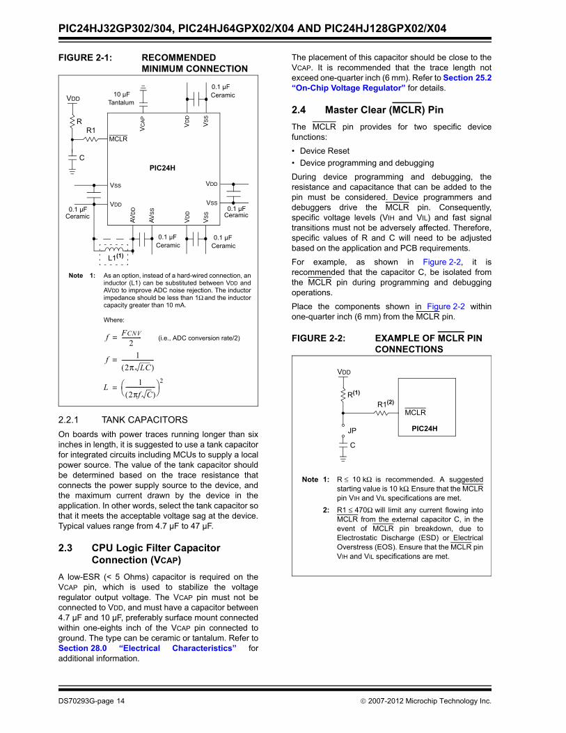
FIGURE 2-1: RECOMMENDED MINIMUM CONNECTION
2.2.1 TANK CAPACITORSOn boards with power traces running longer than sixinches in length, it is suggested to use a tank capacitorfor integrated circuits including MCUs to supply a localpower source. The value of the tank capacitor shouldbe determined based on the trace resistance thatconnects the power supply source to the device, andthe maximum current drawn by the device in theapplication. In other words, select the tank capacitor sothat it meets the acceptable voltage sag at the device.Typical values range from 4.7 µF to 47 µF.
2.3 CPU Logic Filter Capacitor Connection (VCAP)
A low-ESR (< 5 Ohms) capacitor is required on theVCAP pin, which is used to stabilize the voltageregulator output voltage. The VCAP pin must not beconnected to VDD, and must have a capacitor between4.7 µF and 10 µF, preferably surface mount connectedwithin one-eights inch of the VCAP pin connected toground. The type can be ceramic or tantalum. Refer toSection 28.0 “Electrical Characteristics” foradditional information.
The placement of this capacitor should be close to theVCAP. It is recommended that the trace length notexceed one-quarter inch (6 mm). Refer to Section 25.2“On-Chip Voltage Regulator” for details.
2.4 Master Clear (MCLR) PinThe MCLR pin provides for two specific devicefunctions:
• Device Reset• Device programming and debugging
During device programming and debugging, theresistance and capacitance that can be added to thepin must be considered. Device programmers anddebuggers drive the MCLR pin. Consequently,specific voltage levels (VIH and VIL) and fast signaltransitions must not be adversely affected. Therefore,specific values of R and C will need to be adjustedbased on the application and PCB requirements.
For example, as shown in Figure 2-2, it isrecommended that the capacitor C, be isolated fromthe MCLR pin during programming and debuggingoperations.
Place the components shown in Figure 2-2 withinone-quarter inch (6 mm) from the MCLR pin.
FIGURE 2-2: EXAMPLE OF MCLR PIN CONNECTIONS
PIC24H
VD
D
VS
S
VDD
VSS
VSS
VDD
AVD
D
AVS
S
VD
D
VS
S0.1 µF
Ceramic0.1 µF
Ceramic
0.1 µFCeramic
0.1 µFCeramic
C
R
VDD
MCLR
0.1 µFCeramic
VC
AP
L1(1)
R1
10 µFTantalum
Note 1: As an option, instead of a hard-wired connection, aninductor (L1) can be substituted between VDD andAVDD to improve ADC noise rejection. The inductorimpedance should be less than 1Ω and the inductorcapacity greater than 10 mA.
Where:
f FCNV2
--------------=
f 12π LC( )
-----------------------=
L 12πf C( )
---------------------⎝ ⎠⎛ ⎞ 2
=
(i.e., ADC conversion rate/2)
Note 1: R ≤ 10 kΩ is recommended. A suggestedstarting value is 10 kΩ. Ensure that the MCLRpin VIH and VIL specifications are met.
2: R1 ≤ 470Ω will limit any current flowing intoMCLR from the external capacitor C, in theevent of MCLR pin breakdown, due toElectrostatic Discharge (ESD) or ElectricalOverstress (EOS). Ensure that the MCLR pinVIH and VIL specifications are met.
PIC24HJ32GP302/304, PIC24HJ64GPX02/X04 AND PIC24HJ128GPX02/X04
2.5 ICSP PinsThe PGECx and PGEDx pins are used for In-CircuitSerial Programming™ (ICSP™) and debuggingpurposes. It is recommended to keep the trace lengthbetween the ICSP connector and the ICSP pins on thedevice as short as possible. If the ICSP connector isexpected to experience an ESD event, a series resistoris recommended, with the value in the range of a fewtens of Ohms, not to exceed 100 Ohms.
Pull-up resistors, series diodes, and capacitors on thePGECx and PGEDx pins are not recommended as theywill interfere with the programmer/debuggercommunications to the device. If such discretecomponents are an application requirement, theyshould be removed from the circuit duringprogramming and debugging. Alternatively, refer to theAC/DC characteristics and timing requirementsinformation in the respective device Flashprogramming specification for information oncapacitive loading limits and pin input voltage high (VIH)and input low (VIL) requirements.
Ensure that the “Communication Channel Select”(i.e., PGECx/PGEDx pins) programmed into the devicematches the physical connections for the ICSP toMPLAB® ICD 3 or MPLAB REAL ICE™.
For more information on ICD 3 and REAL ICEconnection requirements, refer to the followingdocuments that are available on the Microchip website.
Guide” DS51616• “Using MPLAB® REAL ICE™” (poster) DS51749
2.6 External Oscillator PinsMany MCUs have options for at least two oscillators: ahigh-frequency primary oscillator and a low-frequencysecondary oscillator (refer to Section 9.0 “OscillatorConfiguration” for details).
The oscillator circuit should be placed on the sameside of the board as the device. Also, place theoscillator circuit close to the respective oscillator pins,not exceeding one-half inch (12 mm) distancebetween them. The load capacitors should be placednext to the oscillator itself, on the same side of theboard. Use a grounded copper pour around theoscillator circuit to isolate them from surroundingcircuits. The grounded copper pour should be routeddirectly to the MCU ground. Do not run any signaltraces or power traces inside the ground pour. Also, ifusing a two-sided board, avoid any traces on theother side of the board where the crystal is placed. Asuggested layout is shown in Figure 2-3.Recommendations for crystals and ceramicresonators are provided in Table 2-1 and Table 2-2,respectively.
FIGURE 2-3: SUGGESTED PLACEMENT OF THE OSCILLATOR CIRCUIT
TABLE 2-1: CRYSTAL RECOMMENDATIONS
13Main Oscillator
Guard Ring
Guard Trace
SecondaryOscillator
14
15
16
17
18
19
20
PartNumber Vendor Freq. Load
Cap.Package
CaseFrequencyTolerance
MountingType
OperatingTemperature
ECS-40-20-4DN ECS Inc. 4 MHz 20 pF HC49/US ±30 ppm TH -40°C to +85°CECS-80-18-4DN ECS Inc. 8 MHz 18 pF HC49/US ±30 ppm TH -40°C to +85°C
ECS-100-18-4-DN ECS Inc. 10 MHz 18 pF HC49/US ±30 ppm TH -40°C to +85°C
ECS-200-20-4DN ECS Inc. 20 MHz 20 pF HC49/US ±30 ppm TH -40°C to +85°C
ECS-40-20-5G3XDS-TR ECS Inc. 4 MHz 20 pF HC49/US ±30 ppm SM -40°C to +125°C
ECS-80-20-5G3XDS-TR ECS Inc. 8 MHz 20 pF HC49/US ±30 ppm SM -40°C to +125°C
ECS-100-20-5G3XDS-TR ECS Inc. 10 MHz 20 pF HC49/US ±30 ppm SM -40°C to +125°C
ECS-200-20-5G3XDS-TR ECS Inc. 20 MHz 20 pF HC49/US ±30 ppm SM -40°C to 125°C
NX3225SA 20MHZ AT-W NDK 20 MHz 8 pF 3.2 mm x 2.5 mm ±50 ppm SM -40°C to 125°C
PIC24HJ32GP302/304, PIC24HJ64GPX02/X04 AND PIC24HJ128GPX02/X04
TABLE 2-2: RESONATOR RECOMMENDATIONS
2.7 Oscillator Value Conditions on Device Start-up
If the PLL of the target device is enabled andconfigured for the device start-up oscillator, themaximum oscillator source frequency must be limitedto ≤ 8 MHz for start-up with the PLL enabled to complywith device PLL start-up conditions. This means that ifthe external oscillator frequency is outside this range,the application must start-up in the FRC mode first. Thedefault PLL settings after a POR with an oscillatorfrequency outside this range will violate the deviceoperating speed.
Once the device powers up, the application firmwarecan initialize the PLL SFRs, CLKDIV and PLLDBF to asuitable value, and then perform a clock switch to theOscillator + PLL clock source. Note that clock switchingmust be enabled in the device Configuration word.
2.8 Configuration of Analog and Digital Pins During ICSP Operations
If MPLAB ICD 3 or REAL ICE is selected as a debug-ger, it automatically initializes all of the A/D input pins(ANx) as “digital” pins, by setting all bits in theAD1PCFGL register.
The bits in this register that correspond to the A/D pinsthat are initialized by MPLAB ICD 3 or REAL ICE, mustnot be cleared by the user application firmware;otherwise, communication errors will result betweenthe debugger and the device.
If your application needs to use certain A/D pins asanalog input pins during the debug session, the userapplication must clear the corresponding bits in theAD1PCFGL register during initialization of the ADCmodule.
When MPLAB ICD 3 or REAL ICE is used as aprogrammer, the user application firmware mustcorrectly configure the AD1PCFGL register. Automaticinitialization of this register is only done duringdebugger operation. Failure to correctly configure theregister(s) will result in all A/D pins being recognized asanalog input pins, resulting in the port value being readas a logic ‘0’, which may affect user applicationfunctionality.
2.9 Unused I/OsUnused I/O pins should be configured as outputs anddriven to a logic-low state.
Alternatively, connect a 1k to 10k resistor between VSSand the unused pins.
PIC24HJ32GP302/304, PIC24HJ64GPX02/X04 AND PIC24HJ128GPX02/X04
3.0 CPU
3.1 OverviewThe PIC24HJ32GP302/304, PIC24HJ64GPX02/X04and PIC24HJ128GPX02/X04 CPU module has a 16-bit(data) modified Harvard architecture with an enhancedinstruction set and addressing modes. The CPU has a24-bit instruction word with a variable length opcodefield. The Program Counter (PC) is 23 bits wide andaddresses up to 4M x 24 bits of user program memoryspace. The actual amount of program memoryimplemented varies by device. A single-cycleinstruction prefetch mechanism is used to helpmaintain throughput and provides predictableexecution. All instructions execute in a single cycle,with the exception of instructions that change theprogram flow, the double word move (MOV.D)instruction and the table instructions. Overhead-free,single-cycle program loop constructs are supportedusing the REPEAT instruction, which is interruptible atany point.
The PIC24HJ32GP302/304, PIC24HJ64GPX02/X04and PIC24HJ128GPX02/X04 devices have sixteen,16-bit working registers in the programmer’s model.Each of the working registers can serve as a data,address or address offset register. The 16th workingregister (W15) operates as a software Stack Pointer(SP) for interrupts and calls.
The PIC24HJ32GP302/304, PIC24HJ64GPX02/X04and PIC24HJ128GPX02/X04 instruction set includesmany addressing modes and is designed for optimumC compiler efficiency. For most instructions, thePIC24HJ32GP302/304, PIC24HJ64GPX02/X04 andPIC24HJ128GPX02/X04 is capable of executing a data(or program data) memory read, a working register(data) read, a data memory write and a program(instruction) memory read per instruction cycle. As aresult, three parameter instructions can be supported,allowing A + B = C operations to be executed in a singlecycle.
A block diagram of the CPU is shown in Figure 3-1, andthe programmer’s model for the PIC24HJ32GP302/304, PIC24HJ64GPX02/X04 and PIC24HJ128GPX02/X04 is shown in Figure 3-2.
3.2 Data Addressing OverviewThe data space can be linearly addressed as 32K wordsor 64 Kbytes using an Address Generation Unit (AGU).The upper 32 Kbytes of the data space memory map canoptionally be mapped into program space at any 16Kprogram word boundary defined by the 8-bit ProgramSpace Visibility Page (PSVPAG) register. The program todata space mapping feature lets any instruction accessprogram space as if it were data space.
The data space also includes 2 Kbytes of DMA RAM,which is primarily used for DMA data transfers, but maybe used as general purpose RAM.
Note 1: This data sheet summarizes the featuresof the PIC24HJ32GP302/304,PIC24HJ64GPX02/X04 andPIC24HJ128GPX02/X04 families ofdevices. It is not intended to be a compre-hensive reference source. To comple-ment the information in this data sheet,refer to Section 2. “CPU” (DS70204) ofthe “dsPIC33F/PIC24H Family ReferenceManual”, which is available from theMicrochip web site (www.microchip.com).
2: Some registers and associated bitsdescribed in this section may not beavailable on all devices. Refer toSection 4.0 “Memory Organization” inthis data sheet for device-specific registerand bit information.
PIC24HJ32GP302/304, PIC24HJ64GPX02/X04 AND PIC24HJ128GPX02/X04
3.3 Special MCU FeaturesThe PIC24HJ32GP302/304, PIC24HJ64GPX02/X04and PIC24HJ128GPX02/X04 features a 17-bit by 17-bit, single-cycle multiplier. The multiplier can performsigned, unsigned and mixed-sign multiplication. Usinga 17-bit by 17-bit multiplier for 16-bit by 16-bitmultiplication makes mixed-sign multiplicationpossible.
The PIC24HJ32GP302/304, PIC24HJ64GPX02/X04and PIC24HJ128GPX02/X04 devices support 16/16and 32/16 integer divide operations. All divideinstructions are iterative operations. They must beexecuted within a REPEAT loop, resulting in a totalexecution time of 19 instruction cycles. The divideoperation can be interrupted during any of those19 cycles without loss of data.
A multi-bit data shifter is used to perform up to a 16-bit,left or right shift in a single cycle.
FIGURE 3-1: PIC24HJ32GP302/304, PIC24HJ64GPX02/X04 AND PIC24HJ128GPX02/X04 CPU CORE BLOCK DIAGRAM
PIC24HJ32GP302/304, PIC24HJ64GPX02/X04 AND PIC24HJ128GPX02/X04
3.4 CPU ResourcesMany useful resources related to the CPU are providedon the main product page of the Microchip web site forthe devices listed in this data sheet. This product page,which can be accessed using this link, contains thelatest updates and additional information.
3.4.1 KEY RESOURCES• Section 2. “CPU” (DS70204)• Code Samples• Application Notes• Software Libraries• Webinars• All related dsPIC33F/PIC24H Family Reference
Manuals Sections• Development Tools
Note: In the event you are not able to access theproduct page using the link above, enterthis URL in your browser:http://www.microchip.com/wwwproducts/Devices.aspx?dDocName=en534555
PIC24HJ32GP302/304, PIC24HJ64GPX02/X04 AND PIC24HJ128GPX02/X04
3.5 CPU Control Registers
REGISTER 3-1: SR: CPU STATUS REGISTER
U-0 U-0 U-0 U-0 U-0 U-0 U-0 R/W-0— — — — — — — DC
bit 15 bit 8
R/W-0(1) R/W-0(2) R/W-0(2) R-0 R/W-0 R/W-0 R/W-0 R/W-0IPL<2:0>(2) RA N OV Z C
bit 7 bit 0
Legend:C = Clear only bit R = Readable bit U = Unimplemented bit, read as ‘0’S = Set only bit W = Writable bit -n = Value at POR‘1’ = Bit is set ‘0’ = Bit is cleared x = Bit is unknown
bit 15-9 Unimplemented: Read as ‘0’bit 8 DC: MCU ALU Half Carry/Borrow bit
1 = A carry-out from the 4th low-order bit (for byte-sized data) or 8th low-order bit (for word-sized data)of the result occurred
0 = No carry-out from the 4th low-order bit (for byte-sized data) or 8th low-order bit (for word-sizeddata) of the result occurred
bit 7-5 IPL<2:0>: CPU Interrupt Priority Level Status bits(2)
111 = CPU Interrupt Priority Level is 7 (15), user interrupts disabled110 = CPU Interrupt Priority Level is 6 (14)101 = CPU Interrupt Priority Level is 5 (13)100 = CPU Interrupt Priority Level is 4 (12)011 = CPU Interrupt Priority Level is 3 (11)010 = CPU Interrupt Priority Level is 2 (10)001 = CPU Interrupt Priority Level is 1 (9)000 = CPU Interrupt Priority Level is 0 (8)
bit 4 RA: REPEAT Loop Active bit1 = REPEAT loop in progress0 = REPEAT loop not in progress
bit 3 N: MCU ALU Negative bit1 = Result was negative0 = Result was non-negative (zero or positive)
bit 2 OV: MCU ALU Overflow bitThis bit is used for signed arithmetic (two’s complement). It indicates an overflow of a magnitude thatcauses the sign bit to change state. 1 = Overflow occurred for signed arithmetic (in this arithmetic operation)0 = No overflow occurred
bit 1 Z: MCU ALU Zero bit1 = An operation that affects the Z bit has set it at some time in the past0 = The most recent operation that affects the Z bit has cleared it (i.e., a non-zero result)
bit 0 C: MCU ALU Carry/Borrow bit1 = A carry-out from the Most Significant bit of the result occurred0 = No carry-out from the Most Significant bit of the result occurred
Note 1: The IPL<2:0> bits are concatenated with the IPL<3> bit (CORCON<3>) to form the CPU Interrupt Priority Level. The value in parentheses indicates the IPL if IPL<3> = 1. User interrupts are disabled when IPL<3> = 1.
2: The IPL<2:0> Status bits are read only when the NSTDIS bit (INTCON1<15>) = 1.
Legend: C = Clear only bitR = Readable bit W = Writable bit -n = Value at POR ‘1’ = Bit is set0’ = Bit is cleared ‘x = Bit is unknown U = Unimplemented bit, read as ‘0’
bit 15-4 Unimplemented: Read as ‘0’bit 3 IPL3: CPU Interrupt Priority Level Status bit 3(1)
1 = CPU interrupt priority level is greater than 70 = CPU interrupt priority level is 7 or less
bit 2 PSV: Program Space Visibility in Data Space Enable bit1 = Program space visible in data space0 = Program space not visible in data space
bit 1-0 Unimplemented: Read as ‘0’
Note 1: The IPL3 bit is concatenated with the IPL<2:0> bits (SR<7:5>) to form the CPU interrupt priority level.
PIC24HJ32GP302/304, PIC24HJ64GPX02/X04 AND PIC24HJ128GPX02/X04
3.6 Arithmetic Logic Unit (ALU)The PIC24HJ32GP302/304, PIC24HJ64GPX02/X04and PIC24HJ128GPX02/X04 ALU is 16 bits wide andis capable of addition, subtraction, bit shifts and logicoperations. Unless otherwise mentioned, arithmeticoperations are two’s complement in nature. Dependingon the operation, the ALU can affect the values of theCarry (C), Zero (Z), Negative (N), Overflow (OV) andDigit Carry (DC) Status bits in the SR register. The Cand DC Status bits operate as Borrow and Digit Borrowbits, respectively, for subtraction operations.
The ALU can perform 8-bit or 16-bit operations,depending on the mode of the instruction that is used.Data for the ALU operation can come from the Wregister array or data memory, depending on theaddressing mode of the instruction. Likewise, outputdata from the ALU can be written to the W register arrayor a data memory location.
For information on the SR bits affected by each instruc-tion, refer to the “16-bit MCU and DSC Programmer’sReference Manual” (DS70157).
The PIC24HJ32GP302/304, PIC24HJ64GPX02/X04and PIC24HJ128GPX02/X04 CPU incorporateshardware support for both multiplication and division.This includes a dedicated hardware multiplier andsupport hardware for 16-bit-divisor division.
3.6.1 MULTIPLIERUsing the high-speed 17-bit x 17-bit multiplier, the ALUsupports unsigned, signed or mixed-sign operation inseveral MCU multiplication modes:
• 16-bit x 16-bit signed• 16-bit x 16-bit unsigned• 16-bit signed x 5-bit (literal) unsigned• 16-bit unsigned x 16-bit unsigned• 16-bit unsigned x 5-bit (literal) unsigned• 16-bit unsigned x 16-bit signed• 8-bit unsigned x 8-bit unsigned
3.6.2 DIVIDERThe divide block supports 32-bit/16-bit and 16-bit/16-bitsigned and unsigned integer divide operations with thefollowing data sizes:
• 32-bit signed/16-bit signed divide• 32-bit unsigned/16-bit unsigned divide• 16-bit signed/16-bit signed divide• 16-bit unsigned/16-bit unsigned divide
The quotient for all divide instructions ends up in W0and the remainder in W1. 16-bit signed and unsignedDIV instructions can specify any W register for boththe 16-bit divisor (Wn) and any W register (aligned)pair (W(m + 1):Wm) for the 32-bit dividend. The dividealgorithm takes one cycle per bit of divisor, so both32-bit/16-bit and 16-bit/16-bit instructions take thesame number of cycles to execute.
3.6.3 MULTI-BIT DATA SHIFTERThe multi-bit data shifter is capable of performing up to16-bit arithmetic or logic right shifts, or up to 16-bit leftshifts in a single cycle. The source can be either aworking register or a memory location.
The shifter requires a signed binary value to determineboth the magnitude (number of bits) and direction of theshift operation. A positive value shifts the operand right.A negative value shifts the operand left. A value of ‘0’does not modify the operand.
PIC24HJ32GP302/304, PIC24HJ64GPX02/X04 AND PIC24HJ128GPX02/X04
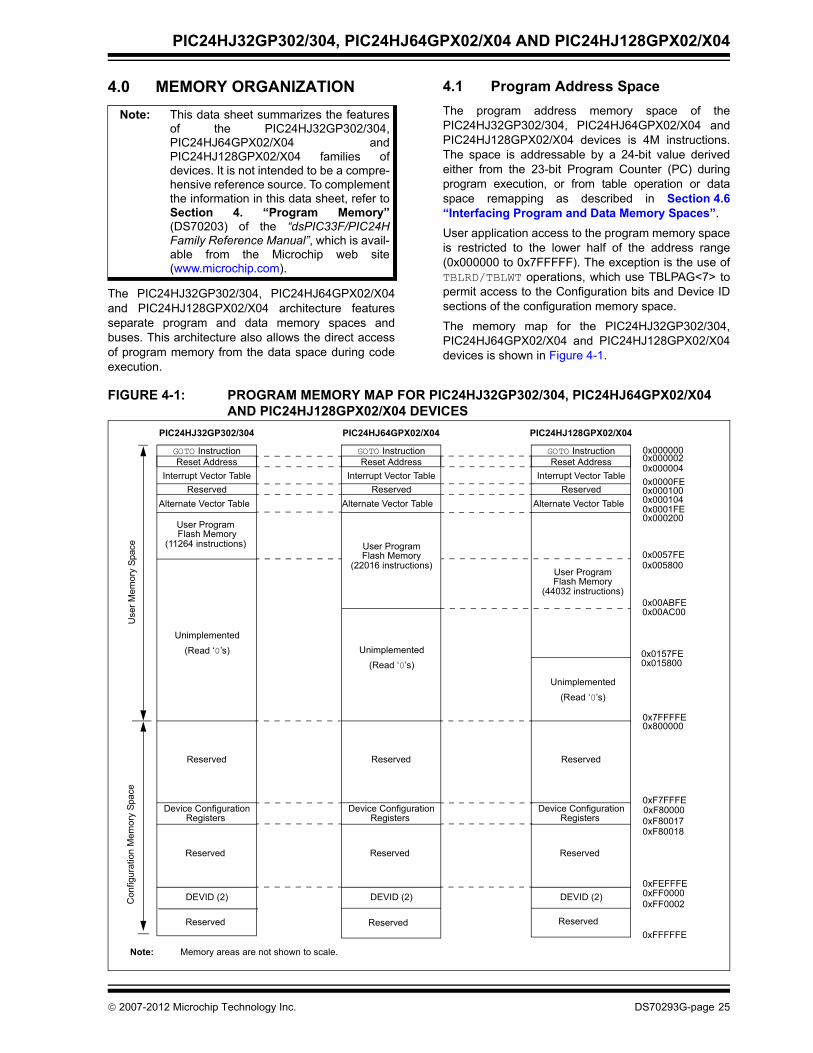
4.0 MEMORY ORGANIZATION
The PIC24HJ32GP302/304, PIC24HJ64GPX02/X04and PIC24HJ128GPX02/X04 architecture featuresseparate program and data memory spaces andbuses. This architecture also allows the direct accessof program memory from the data space during codeexecution.
4.1 Program Address SpaceThe program address memory space of thePIC24HJ32GP302/304, PIC24HJ64GPX02/X04 andPIC24HJ128GPX02/X04 devices is 4M instructions.The space is addressable by a 24-bit value derivedeither from the 23-bit Program Counter (PC) duringprogram execution, or from table operation or dataspace remapping as described in Section 4.6“Interfacing Program and Data Memory Spaces”.
User application access to the program memory spaceis restricted to the lower half of the address range(0x000000 to 0x7FFFFF). The exception is the use ofTBLRD/TBLWT operations, which use TBLPAG<7> topermit access to the Configuration bits and Device IDsections of the configuration memory space.
The memory map for the PIC24HJ32GP302/304,PIC24HJ64GPX02/X04 and PIC24HJ128GPX02/X04devices is shown in Figure 4-1.
FIGURE 4-1: PROGRAM MEMORY MAP FOR PIC24HJ32GP302/304, PIC24HJ64GPX02/X04 AND PIC24HJ128GPX02/X04 DEVICES
Note: This data sheet summarizes the featuresof the PIC24HJ32GP302/304,PIC24HJ64GPX02/X04 andPIC24HJ128GPX02/X04 families ofdevices. It is not intended to be a compre-hensive reference source. To complementthe information in this data sheet, refer toSection 4. “Program Memory”(DS70203) of the “dsPIC33F/PIC24HFamily Reference Manual”, which is avail-able from the Microchip web site(www.microchip.com).
PIC24HJ32GP302/304, PIC24HJ64GPX02/X04 AND PIC24HJ128GPX02/X04
4.1.1 PROGRAM MEMORY ORGANIZATION
The program memory space is organized inword-addressable blocks. Although it is treated as24 bits wide, it is more appropriate to think of eachaddress of the program memory as a lower and upperword, with the upper byte of the upper word beingunimplemented. The lower word always has an evenaddress, while the upper word has an odd address, asshown in Figure 4-2.
Program memory addresses are always word-alignedon the lower word, and addresses are incremented ordecremented by two during code execution. Thisarrangement provides compatibility with data memoryspace addressing and makes data in the programmemory space accessible.
4.1.2 INTERRUPT AND TRAP VECTORSAll PIC24HJ32GP302/304, PIC24HJ64GPX02/X04and PIC24HJ128GPX02/X04 devices reserve theaddresses between 0x00000 and 0x000200 forhard-coded program execution vectors. A hardwareReset vector is provided to redirect code executionfrom the default value of the PC on device Reset to theactual start of code. A GOTO instruction is programmedby the user application at 0x000000, with the actualaddress for the start of code at 0x000002.
PIC24HJ32GP302/304, PIC24HJ64GPX02/X04 andPIC24HJ128GPX02/X04 devices also have twointerrupt vector tables, located from 0x000004 to0x0000FF and 0x000100 to 0x0001FF. These vectortables allow each of the device interrupt sources to behandled by separate Interrupt Service Routines (ISRs).A more detailed discussion of the interrupt vectortables is provided in Section 7.1 “Interrupt VectorTable”.
PIC24HJ32GP302/304, PIC24HJ64GPX02/X04 AND PIC24HJ128GPX02/X04
4.2 Data Address SpaceThe PIC24HJ32GP302/304, PIC24HJ64GPX02/X04and PIC24HJ128GPX02/X04 CPU has a separate16-bit wide data memory space. The data space isaccessed using separate Address Generation Units(AGUs) for read and write operations. The datamemory maps are shown in Figure 4-3 and Figure 4-4.
All Effective Addresses (EAs) in the data memory spaceare 16 bits wide and point to bytes within the data space.This arrangement gives a data space address range of64 Kbytes or 32K words. The lower half of the datamemory space (that is, when EA<15> = 0) is used forimplemented memory addresses, while the upper half(EA<15> = 1) is reserved for the Program SpaceVisibility area (see Section 4.6.3 “Reading Data fromProgram Memory Using Program Space Visibility”).
PIC24HJ32GP302/304, PIC24HJ64GPX02/X04 andPIC24HJ128GPX02/X04 devices implement up to8 Kbytes of data memory. Should an EA point to alocation outside of this area, an all-zero word or byte isreturned.
4.2.1 DATA SPACE WIDTHThe data memory space is organized in byteaddressable, 16-bit wide blocks. Data is aligned in datamemory and registers as 16-bit words, but all dataspace EAs resolve to bytes. The Least SignificantBytes (LSBs) of each word have even addresses, whilethe Most Significant Bytes (MSBs) have oddaddresses.
4.2.2 DATA MEMORY ORGANIZATION AND ALIGNMENT
To maintain backward compatibility with PIC® MCUdevices and improve data space memory usageefficiency, the PIC24HJ32GP302/304,PIC24HJ64GPX02/X04 and PIC24HJ128GPX02/X04instruction set supports both word and byte operations.As a consequence of byte accessibility, all effectiveaddress calculations are internally scaled to stepthrough word-aligned memory. For example, the corerecognizes that Post-Modified Register IndirectAddressing mode [Ws++] results in a value of Ws + 1for byte operations and Ws + 2 for word operations.
A data byte read, reads the complete word thatcontains the byte, using the LSB of any EA todetermine which byte to select. The selected byte isplaced onto the LSB of the data path. That is, datamemory and registers are organized as two parallelbyte-wide entities with shared (word) address decodebut separate write lines. Data byte writes only write tothe corresponding side of the array or register thatmatches the byte address.
All word accesses must be aligned to an even address.Misaligned word data fetches are not supported, socare must be taken when mixing byte and wordoperations, or translating from 8-bit MCU code. If amisaligned read or write is attempted, an address errortrap is generated. If the error occurred on a read, theinstruction underway is completed. If the error occurredon a write, the instruction is executed but the write doesnot occur. In either case, a trap is then executed,allowing the system and/or user application to examinethe machine state prior to execution of the addressFault.
All byte loads into any W register are loaded into theLeast Significant Byte. The Most Significant Byte is notmodified.
A sign-extend instruction (SE) is provided to allow userapplications to translate 8-bit signed data to 16-bitsigned values. Alternatively, for 16-bit unsigned data,user applications can clear the MSB of any W registerby executing a zero-extend (ZE) instruction on theappropriate address.
4.2.3 SFR SPACEThe first 2 Kbytes of the Near Data Space, from 0x0000to 0x07FF, is primarily occupied by Special FunctionRegisters (SFRs). These are used by thePIC24HJ32GP302/304, PIC24HJ64GPX02/X04 andPIC24HJ128GPX02/X04 core and peripheral modulesfor controlling the operation of the device.
SFRs are distributed among the modules that theycontrol, and are generally grouped together by module.Much of the SFR space contains unused addresses;these are read as ‘0’.
4.2.4 NEAR DATA SPACE The 8 Kbyte area between 0x0000 and 0x1FFF isreferred to as the near data space. Locations in thisspace are directly addressable via a 13-bit absoluteaddress field within all memory direct instructions.Additionally, the whole data space is addressable usingMOV instructions, which support Memory DirectAddressing mode with a 16-bit address field, or byusing Indirect Addressing mode using a workingregister as an address pointer.
Note: The actual set of peripheral features andinterrupts varies by the device. Refer tothe corresponding device tables andpinout diagrams for device-specific information.
PIC24HJ32GP302/304, PIC24HJ64GPX02/X04 AND PIC24HJ128GPX02/X04
4.2.5 DMA RAMThe PIC24HJ32GP302/304 devices contain 1 Kbytesof dual ported DMA RAM located at the end of X dataspace. The PIC24HJ64GPX02/X04 andPIC24HJ128GPX02/X04 devices contain 2 Kbytes ofdual ported DMA RAM located at the end of X dataspace, and is a part of X data space. Memorylocations in the DMA RAM space are accessiblesimultaneously by the CPU and the DMA controllermodule. DMA RAM is utilized by the DMA controller tostore data to be transferred to various peripheralsusing DMA, as well as data transferred from variousperipherals using DMA. The DMA RAM can beaccessed by the DMA controller without having tosteal cycles from the CPU.
When the CPU and the DMA controller attempt toconcurrently write to the same DMA RAM location, thehardware ensures that the CPU is given precedence inaccessing the DMA RAM location. Therefore, the DMARAM provides a reliable means of transferring DMAdata without ever having to stall the CPU.
FIGURE 4-3: DATA MEMORY MAP FOR PIC24HJ32GP302/304 DEVICES WITH 4 KB RAM
Note: DMA RAM can be used for generalpurpose data storage if the DMA functionis not required in an application.
PIC24HJ32GP302/304, PIC24HJ64GPX02/X04 AND PIC24HJ128GPX02/X04
FIGURE 4-4: DATA MEMORY MAP FOR PIC24HJ128GP202/204, PIC24HJ64GP202/204, PIC24HJ128GP502/504 AND PIC24HJ64GP502/504 DEVICES WITH 8 KB RAM
4.3 Memory Organization ResourcesMany useful resources related to Memory Organizationare provided on the main product page of the Microchipweb site for the devices listed in this data sheet. Thisproduct page, which can be accessed using this link,contains the latest updates and additional information.
4.3.1 KEY RESOURCES• Section 4. “Program Memory” (DS70203)• Code Samples• Application Notes• Software Libraries• Webinars• All related dsPIC33F/PIC24H Family Reference
Manuals Sections• Development Tools
0x0000
0x07FE
0xFFFE
LSbAddress16 bits
LSbMSb
MSbAddress
0x0001
0x07FF
0xFFFF
OptionallyMappedinto ProgramMemory
0x27FF 0x27FE
0x0801 0x0800
2 KbyteSFR Space
8 Kbyte
SRAM Space
0x8001 0x8000
0x28000x2801
0x1FFE0x2000
0x1FFF0x2001
SpaceDataNear8 Kbyte
SFR Space
X Data RAM (X)
DMA RAM
X DataUnimplemented (X)
Note: In the event you are not able to access theproduct page using the link above, enterthis URL in your browser:http://www.microchip.com/wwwprod-ucts/Devices.aspx?dDoc-Name=en534555
KDIV 0744 ROI DOZE<2:0> DOZEN FRCDIV<2:0> PLLPOST<1:0> —
LFBD 0746 — — — — — — — PLLDIV<8:0>
CTUN 0748 — — — — — — — — — —
gend: x = unknown value on Reset, — = unimplemented, read as ‘0’. Reset values are shown in hexadecimal.te 1: RCON register Reset values dependent on type of Reset.
2: OSCCON register Reset values dependent on the FOSC Configuration bits and by type of Reset.
File Name Addr Bit 15 Bit 14 Bit 13 Bit 12 Bit 11 Bit 10 Bit 9 Bit 8 Bit 7 Bit 6 Bit 5 Bit 4
BSRAM 0750 — — — — — — — — — — — —
SSRAM 0752 — — — — — — — — — — — —
Legend: x = unknown value on Reset, — = unimplemented, read as ‘0’. Reset values are shown in hexadecimal.Note 1: This register is not present in devices with 32K Flash (PIC24HJ32GP302/304).
TABLE 4-33: NVM REGISTER MAP
File Name Addr Bit 15 Bit 14 Bit 13 Bit 12 Bit 11 Bit 10 Bit 9 Bit 8 Bit 7 Bit 6 Bit 5 Bi
NVMCON 0760 WR WREN WRERR — — — — — — ERASE — —
NVMKEY 0766 — — — — — — — — N
Legend: x = unknown value on Reset, — = unimplemented, read as ‘0’. Reset values are shown in hexadecimal.
TABLE 4-34: PMD REGISTER MAP
File Name Addr Bit 15 Bit 14 Bit 13 Bit 12 Bit 11 Bit 10 Bit 9 Bit 8 Bit 7 Bit 6 Bit 5 Bit
Legend: x = unknown value on Reset, — = unimplemented, read as ‘0’. Reset values are shown in hexadecimal.
PIC24HJ32GP302/304, PIC24HJ64GPX02/X04 AND PIC24HJ128GPX02/X04
4.4.1 SOFTWARE STACK
In addition to its use as a working register, the W15register in the PIC24HJ32GP302/304,PIC24HJ64GPX02/X04 and PIC24HJ128GPX02/X04devices is also used as a software Stack Pointer. TheStack Pointer always points to the first available freeword and grows from lower to higher addresses. Itpre-decrements for stack pops and post-increments forstack pushes, as shown in Figure 4-5. For a PC pushduring any CALL instruction, the MSb of the PC iszero-extended before the push, ensuring that the MSbis always clear.
The Stack Pointer Limit register (SPLIM) associatedwith the Stack Pointer sets an upper address boundaryfor the stack. SPLIM is uninitialized at Reset. As is thecase for the Stack Pointer, SPLIM<0> is forced to ‘0’because all stack operations must be word aligned.
Whenever an EA is generated using W15 as a sourceor destination pointer, the resulting address iscompared with the value in SPLIM. If the contents ofthe Stack Pointer (W15) and the SPLIM register areequal and a push operation is performed, a stack errortrap does not occur. The stack error trap occurs on asubsequent push operation. For example, to cause astack error trap when the stack grows beyond address0x2000 in RAM, initialize the SPLIM with the value0x1FFE.
Similarly, a Stack Pointer underflow (stack error) trap isgenerated when the Stack Pointer address is found tobe less than 0x0800. This prevents the stack frominterfering with the Special Function Register (SFR)space.
A write to the SPLIM register should not be immediatelyfollowed by an indirect read operation using W15.
FIGURE 4-5: CALL STACK FRAME
4.4.2 DATA RAM PROTECTION FEATUREThe PIC24H product family supports Data RAMprotection features that enable segments of RAM to beprotected when used in conjunction with Boot andSecure Code Segment Security. BSRAM (Secure RAMsegment for BS) is accessible only from the BootSegment Flash code when enabled. SSRAM (SecureRAM segment for RAM) is accessible only from theSecure Segment Flash code when enabled. SeeTable 4-1 for an overview of the BSRAM and SSRAMSFRs.
4.5 Instruction Addressing ModesThe addressing modes shown in Table 4-35 form thebasis of the addressing modes optimized to support thespecific features of individual instructions. Theaddressing modes provided in the MAC class ofinstructions differ from those in the other instructiontypes.
4.5.1 FILE REGISTER INSTRUCTIONSMost file register instructions use a 13-bit address field(f) to directly address data present in the first 8192bytes of data memory (near data space). Most fileregister instructions employ a working register, W0,which is denoted as WREG in these instructions. Thedestination is typically either the same file register orWREG (with the exception of the MUL instruction),which writes the result to a register or register pair. TheMOV instruction allows additional flexibility and canaccess the entire data space.
4.5.2 MCU INSTRUCTIONSThe three-operand MCU instructions are of the form:Operand 3 = Operand 1 <function> Operand 2
where:
Operand 1 is always a working register (that is, theaddressing mode can only be register direct), which isreferred to as Wb.
Operand 2 can be a W register, fetched from datamemory, or a 5-bit literal. The result location can beeither a W register or a data memory location. The fol-lowing addressing modes are supported by MCUinstructions:
PIC24HJ32GP302/304, PIC24HJ64GPX02/X04 AND PIC24HJ128GPX02/X04
TABLE 4-35: FUNDAMENTAL ADDRESSING MODES SUPPORTED
4.5.3 MOVE (MOV) INSTRUCTIONMove instructions provide a greater degree of address-ing flexibility than other instructions. In addition to theAddressing modes supported by most MCU instruc-tions, MOV instructions also support Register Indirectwith Register Offset Addressing mode, also referred toas Register Indexed mode.
In summary, the following addressing modes aresupported by move instructions:
4.5.4 OTHER INSTRUCTIONSBesides the addressing modes outlined previously, someinstructions use literal constants of various sizes. Forexample, BRA (branch) instructions use 16-bit signed lit-erals to specify the branch destination directly, whereasthe DISI instruction uses a 14-bit unsigned literal field. Insome instructions, such as ADD Acc, the source of anoperand or result is implied by the opcode itself. Certainoperations, such as NOP, do not have any operands.
Addressing Mode Description
File Register Direct The address of the file register is specified explicitly.Register Direct The contents of a register are accessed directly.Register Indirect The contents of Wn forms the Effective Address (EA).Register Indirect Post-Modified The contents of Wn forms the EA. Wn is post-modified (incremented
or decremented) by a constant value.Register Indirect Pre-Modified Wn is pre-modified (incremented or decremented) by a signed constant value
to form the EA.Register Indirect with Register Offset (Register Indexed)
The sum of Wn and Wb forms the EA.
Register Indirect with Literal Offset The sum of Wn and a literal forms the EA.
Note: For the MOV instructions, the addressingmode specified in the instruction can differfor the source and destination EA.However, the 4-bit Wb (Register Offset)field is shared by both source anddestination (but typically only used byone).
Note: Not all instructions support all theaddressing modes given above. Individualinstructions may support different subsetsof these addressing modes.
PIC24HJ32GP302/304, PIC24HJ64GPX02/X04 AND PIC24HJ128GPX02/X04
4.6 Interfacing Program and Data Memory Spaces
The PIC24HJ32GP302/304, PIC24HJ64GPX02/X04and PIC24HJ128GPX02/X04 architecture uses a24-bit-wide program space and a 16-bit-wide dataspace. The architecture is also a modified Harvardscheme, meaning that data can also be present in theprogram space. To use this data successfully, it mustbe accessed in a way that preserves the alignment ofinformation in both spaces.
Aside from normal execution, thePIC24HJ32GP302/304, PIC24HJ64GPX02/X04 andPIC24HJ128GPX02/X04 architecture provides twomethods by which program space can be accessedduring operation:
• Using table instructions to access individual bytes or words anywhere in the program space
• Remapping a portion of the program space into the data space (Program Space Visibility)
Table instructions allow an application to read or writeto small areas of the program memory. This capabilitymakes the method ideal for accessing data tables thatneed to be updated periodically. It also allows accessto all bytes of the program word. The remappingmethod allows an application to access a large block ofdata on a read-only basis, which is ideal for look-upsfrom a large table of static data. The application canonly access the least significant word of the programword.
4.6.1 ADDRESSING PROGRAM SPACESince the address ranges for the data and programspaces are 16 and 24 bits, respectively, a method isneeded to create a 23-bit or 24-bit program addressfrom 16-bit data registers. The solution depends on theinterface method to be used.
For table operations, the 8-bit Table Page register(TBLPAG) is used to define a 32K word region withinthe program space. This is concatenated with a 16-bitEA to arrive at a full 24-bit program space address. Inthis format, the Most Significant bit (MSb) of TBLPAGis used to determine if the operation occurs in the usermemory (TBLPAG<7> = 0) or the configuration mem-ory (TBLPAG<7> = 1).
For remapping operations, the 8-bit Program SpaceVisibility register (PSVPAG) is used to define a16K word page in the program space. When the MSbof the EA is ‘1’, PSVPAG is concatenated with the lower15 bits of the EA to form a 23-bit program spaceaddress. Unlike table operations, this limits remappingoperations strictly to the user memory area.
Table 4-36 and Figure 4-6 show how the program EA iscreated for table operations and remapping accessesfrom the data EA. Here, P<23:0> refers to a programspace word, and D<15:0> refers to a data space word.
TABLE 4-36: PROGRAM SPACE ADDRESS CONSTRUCTION
Access Type AccessSpace
Program Space Address<23> <22:16> <15> <14:1> <0>
Instruction Access(Code Execution)
User 0 PC<22:1> 0
0xx xxxx xxxx xxxx xxxx xxx0
TBLRD/TBLWT(Byte/Word Read/Write)
User TBLPAG<7:0> Data EA<15:0> 0xxx xxxx xxxx xxxx xxxx xxxx
Configuration TBLPAG<7:0> Data EA<15:0> 1xxx xxxx xxxx xxxx xxxx xxxx
Program Space Visibility(Block Remap/Read)
User 0 PSVPAG<7:0> Data EA<14:0>(1)
0 xxxx xxxx xxx xxxx xxxx xxxx
Note 1: Data EA<15> is always ‘1’ in this case, but is not used in calculating the program space address. Bit 15 of the address is PSVPAG<0>.
PIC24HJ32GP302/304, PIC24HJ64GPX02/X04 AND PIC24HJ128GPX02/X04
FIGURE 4-6: DATA ACCESS FROM PROGRAM SPACE ADDRESS GENERATION
0Program Counter
23 bits
1
PSVPAG
8 bits
EA
15 bits
Program Counter(1)
Select
TBLPAG
8 bits
EA
16 bits
Byte Select
0
0
1/0
User/Configuration
Table Operations(2)
Program Space Visibility(1)
Space Select
24 bits
23 bits
(Remapping)
1/0
0
Note 1: The Least Significant bit (LSb) of program space addresses is always fixed as ‘0’ to maintainword alignment of data in the program and data spaces.
2: Table operations are not required to be word aligned. Table read operations are permittedin the configuration memory space.
PIC24HJ32GP302/304, PIC24HJ64GPX02/X04 AND PIC24HJ128GPX02/X04
4.6.2 DATA ACCESS FROM PROGRAM MEMORY USING TABLE INSTRUCTIONS
The TBLRDL and TBLWTL instructions offer a directmethod of reading or writing the lower word of anyaddress within the program space without goingthrough data space. The TBLRDH and TBLWTHinstructions are the only method to read or write theupper 8 bits of a program space word as data.
The PC is incremented by two for each successive24-bit program word. This allows program memoryaddresses to directly map to data space addresses.Program memory can thus be regarded as two 16-bitwide word address spaces, residing side by side, eachwith the same address range. TBLRDL and TBLWTLaccess the space that contains the least significantdata word. TBLRDH and TBLWTH access the space thatcontains the upper data byte.
Two table instructions are provided to move byte orword-sized (16-bit) data to and from program space.Both function as either byte or word operations.
• TBLRDL (Table Read Low):- In Word mode, this instruction maps the
lower word of the program space location (P<15:0>) to a data address (D<15:0>).
- In Byte mode, either the upper or lower byte of the lower program word is mapped to the lower byte of a data address. The upper byte is selected when Byte Select is ‘1’; the lower byte is selected when it is ‘0’.
• TBLRDH (Table Read High):- In Word mode, this instruction maps the entire
upper word of a program address (P<23:16>) to a data address. The ‘phantom’ byte (D<15:8>), is always ‘0’.
- In Byte mode, this instruction maps the upper or lower byte of the program word to D<7:0> of the data address, in the TBLRDL instruc-tion. The data is always ‘0’ when the upper ‘phantom’ byte is selected (Byte Select = 1).
Similarly, two table instructions, TBLWTH and TBLWTL,are used to write individual bytes or words to a pro-gram space address. The details of their operation areexplained in Section 5.0 “Flash Program Memory”.
For all table operations, the area of program memoryspace to be accessed is determined by the Table Pageregister (TBLPAG). TBLPAG covers the entire programmemory space of the device, including user applicationand configuration spaces. When TBLPAG<7> = 0, thetable page is located in the user memory space. WhenTBLPAG<7> = 1, the page is located in configurationspace.
FIGURE 4-7: ACCESSING PROGRAM MEMORY WITH TABLE INSTRUCTIONS
08162300000000
00000000
00000000
00000000
‘Phantom’ Byte
TBLRDH.B (Wn<0> = 0)
TBLRDL.W
TBLRDL.B (Wn<0> = 1)TBLRDL.B (Wn<0> = 0)
23 15 0
TBLPAG02
0x000000
0x800000
0x020000
0x030000
Program Space
The address for the table operation is determined by the data EAwithin the page defined by the TBLPAG register. Only read operations are shown; write operations are also valid inthe user memory area.
PIC24HJ32GP302/304, PIC24HJ64GPX02/X04 AND PIC24HJ128GPX02/X04
4.6.3 READING DATA FROM PROGRAM MEMORY USING PROGRAM SPACE VISIBILITY
The upper 32 Kbytes of data space may optionally bemapped into any 16K word page of the program space.This option provides transparent access to storedconstant data from the data space without the need touse special instructions, such as TBLRDL/TBLRDH.
Program space access through the data space occursif the MSb of the data space EA is ‘1’ and programspace visibility is enabled by setting the PSV bit in theCore Control register (CORCON<2>). The location ofthe program memory space to be mapped into the dataspace is determined by the Program Space VisibilityPage register (PSVPAG). This 8-bit register definesany one of 256 possible pages of 16K words inprogram space. In effect, PSVPAG functions as theupper 8 bits of the program memory address, with the15 bits of the EA functioning as the lower bits. Byincrementing the PC by 2 for each program memoryword, the lower 15 bits of data space addresses directlymap to the lower 15 bits in the corresponding programspace addresses.
Data reads to this area add a cycle to the instructionbeing executed, since two program memory fetchesare required.
Although each data space address 0x8000 and highermaps directly into a corresponding program memoryaddress (see Figure 4-8), only the lower 16 bits of the
24-bit program word are used to contain the data. Theupper 8 bits of any program space location used asdata should be programmed with ‘1111 1111’ or‘0000 0000’ to force a NOP. This prevents possibleissues should the area of code ever be accidentallyexecuted.
For operations that use PSV and are executed outsidea REPEAT loop, the MOV and MOV.D instructionsrequire one instruction cycle in addition to the specifiedexecution time. All other instructions require twoinstruction cycles in addition to the specified executiontime.
For operations that use PSV, and are executed insidea REPEAT loop, these instances require two instructioncycles in addition to the specified execution time of theinstruction:
• Execution in the first iteration• Execution in the last iteration• Execution prior to exiting the loop due to an
interrupt• Execution upon re-entering the loop after an
interrupt is serviced
Any other iteration of the REPEAT loop allows theinstruction using PSV to access data, to execute in asingle cycle.
FIGURE 4-8: PROGRAM SPACE VISIBILITY OPERATION
Note: PSV access is temporarily disabled duringtable reads/writes.
23 15 0PSVPAGData SpaceProgram Space
0x0000
0x8000
0xFFFF
020x000000
0x800000
0x010000
0x018000
When CORCON<2> = 1 and EA<15> = 1:
The data in the page designated by PSVPAG is mapped into the upper half of the data memory space...
Data EA<14:0>
...while the lower 15 bits of the EA specify an exact address within the PSV area. This corresponds exactly to the same lower 15 bits of the actual program space address.
PIC24HJ32GP302/304, PIC24HJ64GPX02/X04 AND PIC24HJ128GPX02/X04
5.0 FLASH PROGRAM MEMORY
The PIC24HJ32GP302/304, PIC24HJ64GPX02/X04and PIC24HJ128GPX02/X04 devices contain internalFlash program memory for storing and executingapplication code. The memory is readable, writable anderasable during normal operation over the entire VDDrange.
Flash memory can be programmed in two ways:
• In-Circuit Serial Programming™ (ICSP™) programming capability
• Run-Time Self-Programming (RTSP)
ICSP allows the PIC24HJ32GP302/304,PIC24HJ64GPX02/X04 and PIC24HJ128GPX02/X04devices to be serially programmed while in the endapplication circuit. This is done with two lines forprogramming clock and programming data (one of thealternate programming pin pairs: PGEC1/PGED1,
PGEC2/PGED2 or PGEC3/PGED3), and three otherlines for power (VDD), ground (VSS) and Master Clear(MCLR). This allows customers to manufacture boardswith unprogrammed devices and then program themicrocontroller just before shipping the product. Thisalso allows the most recent firmware or a customfirmware to be programmed.
RTSP is accomplished using TBLRD (table read) andTBLWT (table write) instructions. With RTSP, the userapplication can write program memory data either inblocks or ‘rows’ of 64 instructions (192 bytes) at a timeor a single program memory word, and erase programmemory in blocks or ‘pages’ of 512 instructions (1536bytes) at a time.
5.1 Table Instructions and Flash Programming
Regardless of the method used, all programming ofFlash memory is done with the table read and tablewrite instructions. These allow direct read and writeaccess to the program memory space from the datamemory while the device is in normal operating mode.The 24-bit target address in the program memory isformed using bits <7:0> of the TBLPAG register and theEffective Address (EA) from a W register specified inthe table instruction, as shown in Figure 5-1.
The TBLRDL and the TBLWTL instructions are used toread or write to bits <15:0> of program memory.TBLRDL and TBLWTL can access program memory inboth Word and Byte modes.
The TBLRDH and TBLWTH instructions are used to reador write to bits <23:16> of program memory. TBLRDHand TBLWTH can also access program memory in Wordor Byte mode.
FIGURE 5-1: ADDRESSING FOR TABLE REGISTERS
Note 1: This data sheet summarizes the featuresof the PIC24HJ32GP302/304,PIC24HJ64GPX02/X04 andPIC24HJ128GPX02/X04 families ofdevices. It is not intended to be acomprehensive reference source. Tocomplement the information in this datasheet, refer to Section 5. “Flash Pro-gramming” (DS70191) of the“dsPIC33F/PIC24H Family ReferenceManual”, which is available from theMicrochip web site (www.microchip.com).
2: Some registers and associated bitsdescribed in this section may not beavailable on all devices. Refer toSection 4.0 “Memory Organization” inthis data sheet for device-specific registerand bit information.
PIC24HJ32GP302/304, PIC24HJ64GPX02/X04 AND PIC24HJ128GPX02/X04
5.2 RTSP OperationThe PIC24HJ32GP302/304, PIC24HJ64GPX02/X04and PIC24HJ128GPX02/X04 Flash program memoryarray is organized into rows of 64 instructions or 192bytes. RTSP allows the user application to erase apage of memory, which consists of eight rows (512instructions) at a time, and to program one row or oneword at a time. Table 28-12 shows typical erase andprogramming times. The 8-row erase pages and singlerow write rows are edge-aligned from the beginning ofprogram memory, on boundaries of 1536 bytes and192 bytes, respectively.
The program memory implements holding buffers thatcan contain 64 instructions of programming data. Priorto the actual programming operation, the write datamust be loaded into the buffers sequentially. Theinstruction words loaded must always be from a groupof 64 boundary.
The basic sequence for RTSP programming is to set upa Table Pointer, then do a series of TBLWT instructionsto load the buffers. Programming is performed bysetting the control bits in the NVMCON register. A totalof 64 TBLWTL and TBLWTH instructions are requiredto load the instructions.
All of the table write operations are single-word writes(two instruction cycles) because only the buffers arewritten. A programming cycle is required forprogramming each row.
5.3 Programming OperationsA complete programming sequence is necessary forprogramming or erasing the internal Flash in RTSPmode. The processor stalls (waits) until theprogramming operation is finished.
The programming time depends on the FRC accuracy(see Table 28-19) and the value of the FRC OscillatorTuning register (see Register 9-4). Use the followingformula to calculate the minimum and maximum valuesfor the Row Write Time, Page Erase Time, and WordWrite Cycle Time parameters (see Table 28-12).
EQUATION 5-1: PROGRAMMING TIME
For example, if the device is operating at +125°C,the FRC accuracy will be ±5%. If the TUN<5:0> bits(see Register 9-4) are set to ‘b111111, theminimum row write time is equal to Equation 5-2.
EQUATION 5-2: MINIMUM ROW WRITE TIME
The maximum row write time is equal to Equation 5-3.
EQUATION 5-3: MAXIMUM ROW WRITE TIME
Setting the WR bit (NVMCON<15>) starts the opera-tion, and the WR bit is automatically cleared when theoperation is finished.
5.4 Control RegistersTwo SFRs are used to read and write the programFlash memory: NVMCON and NVMKEY.
The NVMCON register (Register 5-1) controls whichblocks are to be erased, which memory type is to beprogrammed and the start of the programming cycle.
NVMKEY (Register 5-2) is a write-only register that isused for write protection. To start a programming or erasesequence, the user application must consecutively write0x55 and 0xAA to the NVMKEY register. Refer toSection 5.3 “Programming Operations” for furtherdetails.
5.5 Flash Programming ResourcesMany useful resources related to Flash Programmingare provided on the main product page of the Microchipweb site for the devices listed in this data sheet. Thisproduct page, which can be accessed using this link,contains the latest updates and additional information.
5.5.1 KEY RESOURCES• Section 5. “Flash Programming” (DS70191)• Code Samples• Application Notes• Software Libraries• Webinars• All related dsPIC33F/PIC24H Family Reference
Note: In the event you are not able to access theproduct page using the link above, enterthis URL in your browser:http://www.microchip.com/wwwproducts/Devices.aspx?dDocName=en534555
Legend: SO = Settable only bitR = Readable bit W = Writable bit U = Unimplemented bit, read as ‘0’-n = Value at POR ‘1’ = Bit is set ‘0’ = Bit is cleared x = Bit is unknown
bit 15 WR: Write Control bit1 = Initiates a Flash memory program or erase operation. The operation is self-timed and the bit is
cleared by hardware once operation is complete0 = Program or erase operation is complete and inactive
bit 13 WRERR: Write Sequence Error Flag bit1 = An improper program or erase sequence attempt or termination has occurred (bit is set
automatically on any set attempt of the WR bit)0 = The program or erase operation completed normally
bit 12-7 Unimplemented: Read as ‘0’bit 6 ERASE: Erase/Program Enable bit
1 = Perform the erase operation specified by NVMOP<3:0> on the next WR command0 = Perform the program operation specified by NVMOP<3:0> on the next WR command
bit 5-4 Unimplemented: Read as ‘0’bit 3-0 NVMOP<3:0>: NVM Operation Select bits(2)
If ERASE = 1:1111 = Memory bulk erase operation1110 = Reserved1101 = Erase General Segment1100 = Erase Secure Segment1011 = Reserved0011 = No operation0010 = Memory page erase operation0001 = No operation0000 = Erase a single Configuration register byte
If ERASE = 0:1111 = No operation1110 = Reserved1101 = No operation1100 = No operation1011 = Reserved0011 = Memory word program operation0010 = No operation0001 = Memory row program operation0000 = Program a single Configuration register byte
Note 1: These bits can only be reset on a POR.2: All other combinations of NVMOP<3:0> are unimplemented.
PIC24HJ32GP302/304, PIC24HJ64GPX02/X04 AND PIC24HJ128GPX02/X04
5.6.1 PROGRAMMING ALGORITHM FOR FLASH PROGRAM MEMORY
Programmers can program one row of program Flashmemory at a time. To do this, it is necessary to erasethe 8-row erase page that contains the desired row.The general process is:
1. Read eight rows of program memory(512 instructions) and store in data RAM.
2. Update the program data in RAM with thedesired new data.
3. Erase the block (see Example 5-1):a) Set the NVMOP bits (NVMCON<3:0>) to
‘0010’ to configure for block erase. Set theERASE (NVMCON<6>) and WREN (NVMCON<14>) bits.
b) Write the starting address of the page to beerased into the TBLPAG and W registers.
c) Write 0x55 to NVMKEY.d) Write 0xAA to NVMKEY.e) Set the WR bit (NVMCON<15>). The erase
cycle begins and the CPU stalls for the dura-tion of the erase cycle. When the erase isdone, the WR bit is cleared automatically.
4. Write the first 64 instructions from data RAM intothe program memory buffers (see Example 5-2).
5. Write the program block to Flash memory:a) Set the NVMOP bits to ‘0001’ to configure
for row programming. Clear the ERASE bitand set the WREN bit.
b) Write 0x55 to NVMKEY.c) Write 0xAA to NVMKEY.d) Set the WR bit. The programming cycle
begins and the CPU stalls for the duration ofthe write cycle. When the write to Flash mem-ory is done, the WR bit is clearedautomatically.
6. Repeat steps 4 and 5, using the next available64 instructions from the block in data RAM byincrementing the value in TBLPAG, until all512 instructions are written back to Flash memory.
For protection against accidental operations, the writeinitiate sequence for NVMKEY must be used to allowany erase or program operation to proceed. After theprogramming command has been executed, the userapplication must wait for the programming time untilprogramming is complete. The two instructionsfollowing the start of the programming sequenceshould be NOPs, as shown in Example 5-3.
EXAMPLE 5-1: ERASING A PROGRAM MEMORY PAGE ; Set up NVMCON for block erase operation
; Init pointer to row to be ERASEDMOV #tblpage(PROG_ADDR), W0 ; MOV W0, TBLPAG ; Initialize PM Page Boundary SFRMOV #tbloffset(PROG_ADDR), W0 ; Initialize in-page EA[15:0] pointerTBLWTL W0, [W0] ; Set base address of erase blockDISI #5 ; Block all interrupts with priority <7
; for next 5 instructionsMOV #0x55, W0 MOV W0, NVMKEY ; Write the 55 key MOV #0xAA, W1 ;MOV W1, NVMKEY ; Write the AA keyBSET NVMCON, #WR ; Start the erase sequence NOP ; Insert two NOPs after the eraseNOP ; command is asserted
PIC24HJ32GP302/304, PIC24HJ64GPX02/X04 AND PIC24HJ128GPX02/X04
EXAMPLE 5-2: LOADING THE WRITE BUFFERS
EXAMPLE 5-3: INITIATING A PROGRAMMING SEQUENCE
; Set up NVMCON for row programming operationsMOV #0x4001, W0 ;MOV W0, NVMCON ; Initialize NVMCON
; Set up a pointer to the first program memory location to be written; program memory selected, and writes enabled
MOV #0x0000, W0 ; MOV W0, TBLPAG ; Initialize PM Page Boundary SFRMOV #0x6000, W0 ; An example program memory address
; Perform the TBLWT instructions to write the latches; 0th_program_word
MOV #LOW_WORD_0, W2 ; MOV #HIGH_BYTE_0, W3 ; TBLWTL W2, [W0] ; Write PM low word into program latchTBLWTH W3, [W0++] ; Write PM high byte into program latch
; 1st_program_wordMOV #LOW_WORD_1, W2 ; MOV #HIGH_BYTE_1, W3 ; TBLWTL W2, [W0] ; Write PM low word into program latchTBLWTH W3, [W0++] ; Write PM high byte into program latch
; 2nd_program_wordMOV #LOW_WORD_2, W2 ; MOV #HIGH_BYTE_2, W3 ; TBLWTL W2, [W0] ; Write PM low word into program latchTBLWTH W3, [W0++] ; Write PM high byte into program latch•••
; 63rd_program_wordMOV #LOW_WORD_31, W2 ; MOV #HIGH_BYTE_31, W3 ; TBLWTL W2, [W0] ; Write PM low word into program latchTBLWTH W3, [W0++] ; Write PM high byte into program latch
DISI #5 ; Block all interrupts with priority <7; for next 5 instructions
MOV #0x55, W0MOV W0, NVMKEY ; Write the 55 key MOV #0xAA, W1 ;MOV W1, NVMKEY ; Write the AA keyBSET NVMCON, #WR ; Start the erase sequence NOP ; Insert two NOPs after theNOP ; erase command is asserted
- Illegal Opcode Reset- Uninitialized W Register Reset- Security Reset
A simplified block diagram of the Reset module isshown in Figure 6-1.
Any active source of reset will make the SYSRSTsignal active. On system Reset, some of the registersassociated with the CPU and peripherals are forced toa known Reset state and some are unaffected.
All types of device Reset sets a corresponding statusbit in the RCON register to indicate the type of Reset(see Register 6-1).
A POR clears all the bits, except for the POR bit(RCON<0>), that are set. The user application can setor clear any bit at any time during code execution. TheRCON bits only serve as status bits. Setting a particularReset status bit in software does not cause a deviceReset to occur.
The RCON register also has other bits associated withthe Watchdog Timer and device power-saving states.The function of these bits is discussed in other sectionsof this manual.
FIGURE 6-1: RESET SYSTEM BLOCK DIAGRAM
Note 1: This data sheet summarizes the featuresof the PIC24HJ32GP302/304,PIC24HJ64GPX02/X04 andPIC24HJ128GPX02/X04 families ofdevices. It is not intended to be a compre-hensive reference source. To comple-ment the information in this data sheet,refer to Section 8. “Reset” (DS70192) ofthe “dsPIC33F/PIC24H Family ReferenceManual”, which is available from theMicrochip web site (www.microchip.com).
2: Some registers and associated bitsdescribed in this section may not beavailable on all devices. Refer toSection 4.0 “Memory Organization” inthis data sheet for device-specific registerand bit information.
Note: Refer to the specific peripheral section orSection 3.0 “CPU” of this manual forregister Reset states.
Note: The status bits in the RCON registershould be cleared after they are read sothat the next RCON register value after adevice Reset is meaningful.
PIC24HJ32GP302/304, PIC24HJ64GPX02/X04 AND PIC24HJ128GPX02/X04
6.1 Reset ResourcesMany useful resources related to Resets are providedon the main product page of the Microchip web site forthe devices listed in this data sheet. This product page,which can be accessed using this link, contains thelatest updates and additional information.
6.1.1 KEY RESOURCES• Section 8. “Resets” (DS70192)• Code Samples• Application Notes• Software Libraries• Webinars• All related dsPIC33F/PIC24H Family Reference
Manuals Sections• Development Tools
Note: In the event you are not able to access theproduct page using the link above, enterthis URL in your browser:http://www.microchip.com/wwwproducts/Devices.aspx?dDocName=en534555
R/W-0 R/W-0 R/W-0 R/W-0 R/W-0 R/W-0 R/W-1 R/W-1EXTR SWR SWDTEN(2) WDTO SLEEP IDLE BOR POR
bit 7 bit 0
Legend:R = Readable bit W = Writable bit U = Unimplemented bit, read as ‘0’-n = Value at POR ‘1’ = Bit is set ‘0’ = Bit is cleared x = Bit is unknown
bit 15 TRAPR: Trap Reset Flag bit1 = A Trap Conflict Reset has occurred0 = A Trap Conflict Reset has not occurred
bit 14 IOPUWR: Illegal Opcode or Uninitialized W Access Reset Flag bit1 = An illegal opcode detection, an illegal address mode or uninitialized W register used as an
Address Pointer caused a Reset0 = An illegal opcode or uninitialized W Reset has not occurred
bit 13-10 Unimplemented: Read as ‘0’bit 9 CM: Configuration Mismatch Flag bit
1 = A configuration mismatch Reset has occurred.0 = A configuration mismatch Reset has NOT occurred
bit 8 VREGS: Voltage Regulator Standby During Sleep bit1 = Voltage regulator is active during Sleep0 = Voltage regulator goes into Standby mode during Sleep
bit 7 EXTR: External Reset (MCLR) Pin bit1 = A Master Clear (pin) Reset has occurred0 = A Master Clear (pin) Reset has not occurred
bit 6 SWR: Software Reset (Instruction) Flag bit1 = A RESET instruction has been executed0 = A RESET instruction has not been executed
bit 5 SWDTEN: Software Enable/Disable of WDT bit(2)
1 = WDT is enabled0 = WDT is disabled
bit 4 WDTO: Watchdog Timer Time-out Flag bit1 = WDT time-out has occurred0 = WDT time-out has not occurred
bit 3 SLEEP: Wake-up from Sleep Flag bit1 = Device has been in Sleep mode0 = Device has not been in Sleep mode
bit 2 IDLE: Wake-up from Idle Flag bit1 = Device was in Idle mode0 = Device was not in Idle mode
Note 1: All of the Reset status bits can be set or cleared in software. Setting one of these bits in software does not cause a device Reset.
2: If the FWDTEN Configuration bit is ‘1’ (unprogrammed), the WDT is always enabled, regardless of the SWDTEN bit setting.
PIC24HJ32GP302/304, PIC24HJ64GPX02/X04 AND PIC24HJ128GPX02/X04
6.3 System ResetThe PIC24HJ32GP302/304, PIC24HJ64GPX02/X04and PIC24HJ128GPX02/X04 family of devices havetwo types of Reset:
• Cold Reset• Warm Reset
A cold Reset is the result of a Power-on Reset (POR)or a Brown-out Reset (BOR). On a cold Reset, theFNOSC configuration bits in the FOSC deviceconfiguration register selects the device clock source.
A warm Reset is the result of all other reset sources,including the RESET instruction. On warm Reset, thedevice will continue to operate from the current clocksource as indicated by the Current Oscillator Selectionbits (COSC<2:0>) in the Oscillator Control register(OSCCON<14:12>).
The device is kept in a Reset state until the systempower supplies have stabilized at appropriate levelsand the oscillator clock is ready. A description of thesequence in which this occurs and is shown inFigure 6-2.
TABLE 6-1: OSCILLATOR DELAY
Oscillator Mode Oscillator Startup Delay
Oscillator Startup Timer PLL Lock Time Total Delay
Note 1: TOSCD = Oscillator Start-up Delay (1.1 μs max for FRC, 70 μs max for LPRC). Crystal Oscillator start-up times vary with crystal characteristics, load capacitance, etc.
2: TOST = Oscillator Start-up Timer Delay (1024 oscillator clock period). For example, TOST = 102.4 μs for a 10 MHz crystal and TOST = 32 ms for a 32 kHz crystal.
3: TLOCK = PLL lock time (1.5 ms nominal), if PLL is enabled.
PIC24HJ32GP302/304, PIC24HJ64GPX02/X04 AND PIC24HJ128GPX02/X04
FIGURE 6-2: SYSTEM RESET TIMING
Reset RunDevice Status
VDD
VPOR
VborVBOR
POR
BOR
SYSRST
TPWRT
TPOR
TBOR
Oscillator Clock
TOSCD TOST TLOCK
Time
FSCMTFSCM
1
23
4
5
6
Note 1: POR: A POR circuit holds the device in Reset when the power supply is turned on. The POR circuit is activeuntil VDD crosses the VPOR threshold and the delay TPOR has elapsed.
2: BOR: The on-chip voltage regulator has a BOR circuit that keeps the device in Reset until VDD crosses theVBOR threshold and the delay TBOR has elapsed. The delay TBOR ensures the voltage regulator outputbecomes stable.
3: PWRT Timer: The programmable power-up timer continues to hold the processor in Reset for a specificperiod of time (TPWRT) after a BOR. The delay TPWRT ensures that the system power supplies have stabilizedat the appropriate level for full-speed operation. After the delay TPWRT has elapsed, the SYSRST becomesinactive, which in turn enables the selected oscillator to start generating clock cycles.
4: Oscillator Delay: The total delay for the clock to be ready for various clock source selections are given inTable 6-1. Refer to Section 9.0 “Oscillator Configuration” for more information.
5: When the oscillator clock is ready, the processor begins execution from location 0x000000. The userapplication programs a GOTO instruction at the reset address, which redirects program execution to theappropriate start-up routine.
6: The Fail-Safe Clock Monitor (FSCM), if enabled, begins to monitor the system clock when the system clockis ready and the delay TFSCM elapsed.
PIC24HJ32GP302/304, PIC24HJ64GPX02/X04 AND PIC24HJ128GPX02/X04
6.4 Power-on Reset (POR)A Power-on Reset (POR) circuit ensures the device isreset from power-on. The POR circuit is active untilVDD crosses the VPOR threshold and the delay TPORhas elapsed. The delay TPOR ensures the internaldevice bias circuits become stable.
The device supply voltage characteristics must meetthe specified starting voltage and rise raterequirements to generate the POR. Refer toSection 28.0 “Electrical Characteristics” for details.
The POR status bit (POR) in the Reset Control register(RCON<0>) is set to indicate the Power-on Reset.
6.4.1 Brown-out Reset (BOR) and Power-up timer (PWRT)
The on-chip regulator has a Brown-out Reset (BOR)circuit that resets the device when the VDD is too low(VDD < VBOR) for proper device operation. The BOR cir-cuit keeps the device in Reset until VDD crosses VBORthreshold and the delay TBOR has elapsed. The delayTBOR ensures the voltage regulator output becomesstable.
The Brown-out Reset status bit (BOR) in the ResetControl register (RCON<1>) is set to indicate the BOR.
The device will not run at full speed after a BOR as theVDD should rise to acceptable levels for full-speedoperation. The PWRT provides power-up time delay(TPWRT) to ensure that the system power supplies havestabilized at the appropriate levels for full-speedoperation before the SYSRST is released.
The power-up timer delay (TPWRT) is programmed bythe Power-on Reset Timer Value Select bits(FPWRT<2:0>) in the POR Configuration register(FPOR<2:0>), which provides eight settings (from 0 msto 128 ms). Refer to Section 25.0 “Special Features”for further details.
Figure 6-3 shows the typical brown-out scenarios. Thereset delay (TBOR + TPWRT) is initiated each time VDDrises above the VBOR trip point
TABLE 6-2: OSCILLATOR DELAYSymbol Parameter Value
VPOR POR threshold 1.8V nominalTPOR POR extension time 30 μs maximumVBOR BOR threshold 2.5V nominalTBOR BOR extension time 100 μs maximumTPWRT Programmable power-up time delay 0-128 ms nominalTFSCM Fail-Safe Clock Monitor Delay 900 μs maximum
Note: When the device exits the Resetcondition (begins normal operation), thedevice operating parameters (voltage,frequency, temperature, etc.) must bewithin their operating ranges, otherwisethe device may not function correctly.The user application must ensure thatthe delay between the time power isfirst applied, and the time SYSRSTbecomes inactive, is long enough to getall operating parameters withinspecification.
PIC24HJ32GP302/304, PIC24HJ64GPX02/X04 AND PIC24HJ128GPX02/X04
FIGURE 6-3: BROWN-OUT SITUATIONS
6.5 External Reset (EXTR)The external Reset is generated by driving the MCLRpin low. The MCLR pin is a Schmitt trigger input with anadditional glitch filter. Reset pulses that are longer thanthe minimum pulse width will generate a Reset. Referto Section 28.0 “Electrical Characteristics” forminimum pulse width specifications. The ExternalReset (MCLR) Pin (EXTR) bit in the Reset Control(RCON) register is set to indicate the MCLR Reset.
6.5.1 EXTERNAL SUPERVISORY CIRCUIT
Many systems have external supervisory circuits thatgenerate reset signals to reset multiple devices in thesystem. This external Reset signal can be directly con-nected to the MCLR pin to reset the device when therest of system is Reset.
6.5.2 INTERNAL SUPERVISORY CIRCUIT
When using the internal power supervisory circuit toreset the device, the external reset pin (MCLR) shouldbe tied directly or resistively to VDD. In this case, theMCLR pin will not be used to generate a Reset. Theexternal reset pin (MCLR) does not have an internalpull-up and must not be left unconnected.
6.6 Software RESET Instruction (SWR)Whenever the RESET instruction is executed, thedevice will assert SYSRST, placing the device in aspecial Reset state. This Reset state will not re-initialize the clock. The clock source in effect prior to theRESET instruction will remain. SYSRST is released atthe next instruction cycle, and the reset vector fetch willcommence.
The Software Reset (Instruction) Flag bit (SWR) in theReset Control register (RCON<6>) is set to indicatethe software Reset.
6.7 Watchdog Time-out Reset (WDTO)Whenever a Watchdog time-out occurs, the device willasynchronously assert SYSRST. The clock source willremain unchanged. A WDT time-out during Sleep orIdle mode will wake-up the processor, but will not resetthe processor.
The Watchdog Timer Time-out Flag bit (WDTO) in theReset Control register (RCON<4>) is set to indicatethe Watchdog Reset. Refer to Section 25.4“Watchdog Timer (WDT)” for more information onWatchdog Reset.
6.8 Trap Conflict Reset If a lower-priority hard trap occurs while a higher-prior-ity trap is being processed, a hard trap conflict Resetoccurs. The hard traps include exceptions of prioritylevel 13 through level 15, inclusive. The address error(level 13) and oscillator error (level 14) traps fall intothis category.
The Trap Reset Flag bit (TRAPR) in the Reset Controlregister (RCON<15>) is set to indicate the Trap ConflictReset. Refer to Section 7.0 “Interrupt Controller” formore information on trap conflict Resets.
PIC24HJ32GP302/304, PIC24HJ64GPX02/X04 AND PIC24HJ128GPX02/X04
6.9 Configuration Mismatch Reset To maintain the integrity of the peripheral pin selectcontrol registers, they are constantly monitored withshadow registers in hardware. If an unexpectedchange in any of the registers occur (such as cell dis-turbances caused by ESD or other external events), aconfiguration mismatch Reset occurs.
The Configuration Mismatch Flag bit (CM) in the ResetControl register (RCON<9>) is set to indicate theconfiguration mismatch Reset. Refer to Section 11.0“I/O Ports” for more information on the configurationmismatch Reset.
6.10 Illegal Condition Device ResetAn illegal condition device Reset occurs due to thefollowing sources:
• Illegal Opcode Reset• Uninitialized W Register Reset• Security Reset
The Illegal Opcode or Uninitialized W Access ResetFlag bit (IOPUWR) in the Reset Control register(RCON<14>) is set to indicate the illegal conditiondevice Reset.
6.10.1 ILLEGAL OPCODE RESET
A device Reset is generated if the device attempts toexecute an illegal opcode value that is fetched fromprogram memory.
The illegal opcode Reset function can prevent thedevice from executing program memory sections thatare used to store constant data. To take advantage ofthe illegal opcode Reset, use only the lower 16 bits of
each program memory section to store the data values.The upper 8 bits should be programmed with 3Fh,which is an illegal opcode value.
6.10.2 UNINITIALIZED W REGISTER RESET
Any attempts to use the uninitialized W register as anaddress pointer will Reset the device. The W registerarray (with the exception of W15) is cleared during allresets and is considered uninitialized until written to.
6.10.3 SECURITY RESET
If a Program Flow Change (PFC) or Vector FlowChange (VFC) targets a restricted location in aprotected segment (Boot and Secure Segment), thatoperation will cause a security Reset.
The PFC occurs when the Program Counter isreloaded as a result of a Call, Jump, Computed Jump,Return, Return from Subroutine, or other form ofbranch instruction.
The VFC occurs when the Program Counter isreloaded with an Interrupt or Trap vector.
Refer to Section 25.8 “Code Protection andCodeGuard™ Security” for more information onSecurity Reset.
6.11 Using the RCON Status BitsThe user application can read the Reset Control regis-ter (RCON) after any device Reset to determine thecause of the reset.
Table 6-3 provides a summary of the reset flag bitoperation.
TABLE 6-3: RESET FLAG BIT OPERATION
Note: The configuration mismatch feature andassociated reset flag is not available on alldevices.
Note: The status bits in the RCON registershould be cleared after they are read sothat the next RCON register value after adevice Reset will be meaningful.
CLRWDT instruction, POR, BORSLEEP (RCON<3>) PWRSAV #SLEEP instruction POR, BORIDLE (RCON<2>) PWRSAV #IDLE instruction POR, BORBOR (RCON<1>) POR, BOR —POR (RCON<0>) POR —Note: All Reset flag bits can be set or cleared by user software.
PIC24HJ32GP302/304, PIC24HJ64GPX02/X04 AND PIC24HJ128GPX02/X04
7.0 INTERRUPT CONTROLLER
The PIC24HJ32GP302/304, PIC24HJ64GPX02/X04and PIC24HJ128GPX02/X04 interrupt controllerreduces the numerous peripheral interrupt request sig-nals to a single interrupt request signal to thePIC24HJ32GP302/304, PIC24HJ64GPX02/X04 andPIC24HJ128GPX02/X04 CPU.
The interrupt controller has the following features:
• Up to eight processor exceptions and software traps
• Eight user-selectable priority levels• Interrupt Vector Table (IVT) with up to 118 vectors• A unique vector for each interrupt or exception
source• Fixed priority within a specified user priority level• Alternate Interrupt Vector Table (AIVT) for debug
support• Fixed interrupt entry and return latencies
7.1 Interrupt Vector TableThe Interrupt Vector Table (IVT), shown in Figure 7-1,resides in program memory, starting at location000004h. The IVT contains 126 vectors consisting ofeight nonmaskable trap vectors plus up to 118 sourcesof interrupt. In general, each interrupt source has itsown vector. Each interrupt vector contains a 24 bit wideaddress. The value programmed into each interruptvector location is the starting address of the associatedInterrupt Service Routine (ISR).
Interrupt vectors are prioritized in terms of their naturalpriority. This priority is linked to their position in thevector table. Lower addresses generally have a highernatural priority. For example, the interrupt associatedwith vector 0 takes priority over interrupts at any othervector address.
PIC24HJ32GP302/304, PIC24HJ64GPX02/X04 andPIC24HJ128GPX02/X04 devices implement up to 45unique interrupts and five nonmaskable traps. Theseare summarized in Table 7-1.
7.1.1 ALTERNATE INTERRUPT VECTOR TABLE
The Alternate Interrupt Vector Table (AIVT) is locatedafter the IVT, as shown in Figure 7-1. Access to theAIVT is provided by the ALTIVT control bit(INTCON2<15>). If the ALTIVT bit is set, all interruptand exception processes use the alternate vectorsinstead of the default vectors. The alternate vectors areorganized in the same manner as the default vectors.
The AIVT supports debugging by providing a means toswitch between an application and a supportenvironment without requiring the interrupt vectors tobe reprogrammed. This feature also enables switchingbetween applications for evaluation of differentsoftware algorithms at run time. If the AIVT is notneeded, the AIVT should be programmed with thesame addresses used in the IVT.
7.2 Reset SequenceA device Reset is not a true exception because theinterrupt controller is not involved in the Reset process.The PIC24HJ32GP302/304, PIC24HJ64GPX02/X04and PIC24HJ128GPX02/X04 device clears itsregisters in response to a Reset, which forces the PCto zero. The microcontroller then begins programexecution at location 0x000000. A GOTO instruction atthe Reset address can redirect program execution tothe appropriate start-up routine.
Note 1: This data sheet summarizes the featuresof the PIC24HJ32GP302/304,PIC24HJ64GPX02/X04 andPIC24HJ128GPX02/X04 families ofdevices. It is not intended to be a compre-hensive reference source. To comple-ment the information in this data sheet,refer to Section 32. “Interrupts (Part III)”(DS70214) of the”dsPIC33F/PIC24HFamily Reference Manual”, which is avail-able from the Microchip web site(www.microchip.com).
2: Some registers and associated bitsdescribed in this section may not beavailable on all devices. Refer toSection 4.0 “Memory Organization” inthis data sheet for device-specific registerand bit information.
Note: Any unimplemented or unused vectorlocations in the IVT and AIVT should beprogrammed with the address of a defaultinterrupt handler routine that contains aRESET instruction.
PIC24HJ32GP302/304, PIC24HJ64GPX02/X04 AND PIC24HJ128GPX02/X04
7.3 Interrupt Control and Status Registers
PIC24HJ32GP302/304, PIC24HJ64GPX02/X04 andPIC24HJ128GPX02/X04 devices implement a total of30 registers for the interrupt controller:
• INTCON1 • INTCON2 • IFSx• IECx• IPCx • INTTREG
7.3.1 INTCON1 AND INTCON2Global interrupt control functions are controlled fromINTCON1 and INTCON2. INTCON1 contains theInterrupt Nesting Disable (NSTDIS) bit as well as thecontrol and status flags for the processor trap sources.The INTCON2 register controls the external interruptrequest signal behavior and the use of the AlternateInterrupt Vector Table.
7.3.2 IFSxThe IFS registers maintain all of the interrupt requestflags. Each source of interrupt has a status bit, which isset by the respective peripherals or external signal andis cleared via software.
7.3.3 IECxThe IEC registers maintain all of the interrupt enablebits. These control bits are used to individually enableinterrupts from the peripherals or external signals.
7.3.4 IPCxThe IPC registers are used to set the interrupt prioritylevel for each source of interrupt. Each user interruptsource can be assigned to one of eight priority levels.
7.3.5 INTTREGThe INTTREG register contains the associatedinterrupt vector number and the new CPU interruptpriority level, which are latched into vector number(VECNUM<6:0>) and Interrupt level (ILR<3:0>) bitfields in the INTTREG register. The new interruptpriority level is the priority of the pending interrupt.
The interrupt sources are assigned to the IFSx, IECxand IPCx registers in the same sequence that they arelisted in Table 7-1. For example, the INT0 (ExternalInterrupt 0) is shown as having vector number 8 and anatural order priority of 0. Thus, the INT0IF bit is foundin IFS0<0>, the INT0IE bit in IEC0<0>, and the INT0IPbits in the first position of IPC0 (IPC0<2:0>).
7.3.6 STATUS/CONTROL REGISTERSAlthough they are not specifically part of the interruptcontrol hardware, two of the CPU Control registerscontain bits that control interrupt functionality.
• The CPU STATUS register, SR, contains the IPL<2:0> bits (SR<7:5>). These bits indicate the current CPU interrupt priority level. The user software can change the current CPU priority level by writing to the IPL bits.
• The CORCON register contains the IPL3 bit which, together with IPL<2:0>, also indicates the current CPU priority level. IPL3 is a read-only bit so that trap events cannot be masked by the user software.
All Interrupt registers are described in Register 7-1through Register 7-29.
7.4 Interrupt ResourcesMany useful resources related Interrupts are providedon the main product page of the Microchip web site forthe devices listed in this data sheet. This product page,which can be accessed using this link, contains thelatest updates and additional information.
7.4.1 KEY RESOURCES• Section 32. “Interrupts (Part III)” (DS70214)• Code Samples• Application Notes• Software Libraries• Webinars• All related dsPIC33F/PIC24H Family Reference
Manuals Sections• Development Tools
Note: In the event you are not able to access theproduct page using the link above, enterthis URL in your browser:http://www.microchip.com/wwwprod-ucts/Devices.aspx?dDoc-Name=en534555
PIC24HJ32GP302/304, PIC24HJ64GPX02/X04 AND PIC24HJ128GPX02/X04
7.5 Interrupt Control Registers
REGISTER 7-1: SR: CPU STATUS REGISTER(1)
U-0 U-0 U-0 U-0 U-0 U-0 U-0 R/W-0— — — — — — — DC
bit 15 bit 8
R/W-0(3) R/W-0(3) R/W-0(3) R-0 R/W-0 R/W-0 R/W-0 R/W-0IPL<2:0>(2) RA N OV Z C
bit 7 bit 0
Legend:C = Clear only bit R = Readable bit U = Unimplemented bit, read as ‘0’S = Set only bit W = Writable bit -n = Value at POR‘1’ = Bit is set ‘0’ = Bit is cleared x = Bit is unknown
bit 7-5 IPL<2:0>: CPU Interrupt Priority Level Status bits(2)
111 = CPU Interrupt Priority Level is 7 (15), user interrupts disabled110 = CPU Interrupt Priority Level is 6 (14)101 = CPU Interrupt Priority Level is 5 (13)100 = CPU Interrupt Priority Level is 4 (12)011 = CPU Interrupt Priority Level is 3 (11)010 = CPU Interrupt Priority Level is 2 (10)001 = CPU Interrupt Priority Level is 1 (9)000 = CPU Interrupt Priority Level is 0 (8)
Note 1: For complete register details, see Register 3-1.2: The IPL<2:0> bits are concatenated with the IPL<3> bit (CORCON<3>) to form the CPU Interrupt Priority
Level. The value in parentheses indicates the IPL if IPL<3> = 1. User interrupts are disabled when IPL<3> = 1.
3: The IPL<2:0> Status bits are read-only when the NSTDIS bit (INTCON1<15>) = 1.
Legend: C = Clear only bitR = Readable bit W = Writable bit -n = Value at POR ‘1’ = Bit is set0’ = Bit is cleared ‘x = Bit is unknown U = Unimplemented bit, read as ‘0’
bit 3 IPL3: CPU Interrupt Priority Level Status bit 3(2)
1 = CPU interrupt priority level is greater than 70 = CPU interrupt priority level is 7 or less
Note 1: For complete register details, see Register 3-2.2: The IPL3 bit is concatenated with the IPL<2:0> bits (SR<7:5>) to form the CPU Interrupt Priority Level.
PIC24HJ32GP302/304, PIC24HJ64GPX02/X04 AND PIC24HJ128GPX02/X04
7.6 Interrupt Setup Procedures
7.6.1 INITIALIZATIONTo configure an interrupt source at initialization:
1. Set the NSTDIS bit (INTCON1<15>) if nestedinterrupts are not desired.
2. Select the user-assigned priority level for theinterrupt source by writing the control bits in theappropriate IPCx register. The priority leveldepends on the specific application and type ofinterrupt source. If multiple priority levels are notdesired, the IPCx register control bits for allenabled interrupt sources can be programmedto the same non-zero value.
3. Clear the interrupt flag status bit associated withthe peripheral in the associated IFSx register.
4. Enable the interrupt source by setting the inter-rupt enable control bit associated with thesource in the appropriate IECx register.
7.6.2 INTERRUPT SERVICE ROUTINEThe method used to declare an ISR and initialize theIVT with the correct vector address depends on theprogramming language (C or assembler) and thelanguage development tool suite used to develop theapplication.
In general, the user application must clear the interruptflag in the appropriate IFSx register for the source ofinterrupt that the ISR handles. Otherwise, the programre-enters the ISR immediately after exiting the routine.If the ISR is coded in assembly language, it must beterminated using a RETFIE instruction to unstack thesaved PC value, SRL value and old CPU priority level.
7.6.3 TRAP SERVICE ROUTINEA Trap Service Routine (TSR) is coded like an ISR,except that the appropriate trap status flag in theINTCON1 register must be cleared to avoid re-entryinto the TSR.
7.6.4 INTERRUPT DISABLEAll user interrupts can be disabled using thisprocedure:
1. Push the current SR value onto the softwarestack using the PUSH instruction.
2. Force the CPU to priority level 7 by inclusiveORing the value 0xOE with SRL.
To enable user interrupts, the POP instruction can beused to restore the previous SR value.
The DISI instruction provides a convenient way todisable interrupts of priority levels 1-6 for a fixed periodof time. Level 7 interrupt sources are not disabled bythe DISI instruction.
Note: At a device Reset, the IPCx registers areinitialized such that all user interruptsources are assigned to priority level 4. Note: Only user interrupts with a priority level of
7 or lower can be disabled. Trap sources(level 8-level 15) cannot be disabled.
PIC24HJ32GP302/304, PIC24HJ64GPX02/X04 AND PIC24HJ128GPX02/X04
8.0 DIRECT MEMORY ACCESS (DMA)
Direct Memory Access (DMA) is a very efficientmechanism of copying data between peripheral SFRs(e.g., UART Receive register, Input Capture 1 buffer),and buffers or variables stored in RAM, with minimalCPU intervention. The DMA controller canautomatically copy entire blocks of data withoutrequiring the user software to read or write theperipheral Special Function Registers (SFRs) everytime a peripheral interrupt occurs. The DMA controlleruses a dedicated bus for data transfers and therefore,does not steal cycles from the code execution flow ofthe CPU. To exploit the DMA capability, thecorresponding user buffers or variables must belocated in DMA RAM.
The PIC24HJ32GP302/304, PIC24HJ64GPX02/X04and PIC24HJ128GPX02/X04 peripherals that canutilize DMA are listed in Table 8-1.
Note 1: This data sheet summarizes the featuresof the PIC24HJ32GP302/304,PIC24HJ64GPX02/X04 andPIC24HJ128GPX02/X04 families ofdevices. It is not intended to be a compre-hensive reference source. To comple-ment the information in this data sheet,refer to Section 38. “Direct MemoryAccess (DMA) (Part III)” (DS70215) ofthe “dsPIC33F/PIC24H Family ReferenceManual”, which is available from theMicrochip web site (www.microchip.com).
2: Some registers and associated bitsdescribed in this section may not beavailable on all devices. Refer toSection 4.0 “Memory Organization” inthis data sheet for device-specific registerand bit information.
TABLE 8-1: DMA CHANNEL TO PERIPHERAL ASSOCIATIONS
Peripheral to DMA Association DMAxREQ RegisterIRQSEL<6:0> Bits
PIC24HJ32GP302/304, PIC24HJ64GPX02/X04 AND PIC24HJ128GPX02/X04
The DMA controller features eight identical datatransfer channels.
Each channel has its own set of control and statusregisters. Each DMA channel can be configured tocopy data either from buffers stored in dual port DMARAM to peripheral SFRs, or from peripheral SFRs tobuffers in DMA RAM.
The DMA controller supports the following features:
• Eight DMA channels• Register Indirect with Post-increment Addressing
generates destination address)• CPU interrupt after half or full block transfer
complete
• Byte or word transfers• Fixed priority channel arbitration• Manual (software) or Automatic (peripheral DMA
requests) transfer initiation• One-Shot or Auto-Repeat block transfer modes• Ping-Pong mode (automatic switch between two
DPSRAM start addresses after each block transfer complete)
• DMA request for each channel can be selected from any supported interrupt source
• Debug support features
For each DMA channel, a DMA interrupt request isgenerated when a block transfer is complete.Alternatively, an interrupt can be generated when half ofthe block has been filled.
FIGURE 8-1: TOP LEVEL SYSTEM ARCHITECTURE USING A DEDICATED TRANSACTION BUS
CPU
SRAM DMA RAM
CPU Peripheral DS Bus
Peripheral 3
DMA
Peripheral
Non-DMA
SRAM X-Bus
PORT 2PORT 1
Peripheral 1
DMAReady
Peripheral 2
DMAReadyReady
Ready
DMA DS Bus
CPU DMA
CPU DMA CPU DMA
Peripheral Indirect Address
DM
AC
ontro
l
DMA Controller
DMAChannels
Note: CPU and DMA address buses are not shown for clarity.
PIC24HJ32GP302/304, PIC24HJ64GPX02/X04 AND PIC24HJ128GPX02/X04
8.1 DMA ResourcesMany useful resources related to DMA are provided onthe main product page of the Microchip web site for thedevices listed in this data sheet. This product page,which can be accessed using this link, contains thelatest updates and additional information.
(Part III)” (DS70215)• Code Samples• Application Notes• Software Libraries• Webinars• All related dsPIC33F/PIC24H Family Reference
Manuals Sections• Development Tools
8.2 DMAC RegistersEach DMAC Channel x (x = 0, 1, 2, 3, 4, 5, 6 or 7)contains the following registers:
• A 16-bit DMA Channel Control register (DMAxCON)
• A 16-bit DMA Channel IRQ Select register (DMAxREQ)
• A 16-bit DMA RAM Primary Start Address register (DMAxSTA)
• A 16-bit DMA RAM Secondary Start Address register (DMAxSTB)
• A 16-bit DMA Peripheral Address register (DMAxPAD)
• A 10-bit DMA Transfer Count register (DMAxCNT)
An additional pair of status registers, DMACS0 andDMACS1, are common to all DMAC channels.DMACS0 contains the DMA RAM and SFR writecollision flags, XWCOLx and PWCOLx, respectively.DMACS1 indicates DMA channel and Ping-Pong modestatus.
The DMAxCON, DMAxREQ, DMAxPAD andDMAxCNT are all conventional read/write registers.Reads of DMAxSTA or DMAxSTB reads the contentsof the DMA RAM Address register. Writes toDMAxSTA or DMAxSTB write to the registers. Thisallows the user to determine the DMA buffer pointervalue (address) at any time.
The interrupt flags (DMAxIF) are located in an IFSxregister in the interrupt controller. The correspondinginterrupt enable control bits (DMAxIE) are located inan IECx register in the interrupt controller, and thecorresponding interrupt priority control bits (DMAxIP)are located in an IPCx register in the interruptcontroller.
Note: In the event you are not able to access theproduct page using the link above, enterthis URL in your browser:http://www.microchip.com/wwwproducts/Devices.aspx?dDocName=en534555
bit 14 SIZE: Data Transfer Size bit1 = Byte0 = Word
bit 13 DIR: Transfer Direction bit (source/destination bus select)1 = Read from DMA RAM address, write to peripheral address0 = Read from peripheral address, write to DMA RAM address
bit 12 HALF: Early Block Transfer Complete Interrupt Select bit1 = Initiate block transfer complete interrupt when half of the data has been moved0 = Initiate block transfer complete interrupt when all of the data has been moved
bit 11 NULLW: Null Data Peripheral Write Mode Select bit1 = Null data write to peripheral in addition to DMA RAM write (DIR bit must also be clear) 0 = Normal operation
bit 10-6 Unimplemented: Read as ‘0’bit 5-4 AMODE<1:0>: DMA Channel Operating Mode Select bits
11 = Reserved (acts as Peripheral Indirect Addressing mode)10 = Peripheral Indirect Addressing mode01 = Register Indirect without Post-Increment mode00 = Register Indirect with Post-Increment mode
bit 3-2 Unimplemented: Read as ‘0’bit 1-0 MODE<1:0>: DMA Channel Operating Mode Select bits
Legend:R = Readable bit W = Writable bit U = Unimplemented bit, read as ‘0’-n = Value at POR ‘1’ = Bit is set ‘0’ = Bit is cleared x = Bit is unknown
bit 15-0 STA<15:0>: Primary DMA RAM Start Address bits (source or destination)
Note 1: A read of this address register returns the current contents of the DMA RAM Address register, not the con-tents written to STA<15:0>. If the channel is enabled (i.e., active), writes to this register may result in unpredictable behavior of the DMA channel and should be avoided.
Legend:R = Readable bit W = Writable bit U = Unimplemented bit, read as ‘0’-n = Value at POR ‘1’ = Bit is set ‘0’ = Bit is cleared x = Bit is unknown
bit 15-0 STB<15:0>: Secondary DMA RAM Start Address bits (source or destination)
Note 1: A read of this address register returns the current contents of the DMA RAM Address register, not the con-tents written to STB<15:0>. If the channel is enabled (i.e., active), writes to this register may result in unpredictable behavior of the DMA channel and should be avoided.
Legend:R = Readable bit W = Writable bit U = Unimplemented bit, read as ‘0’-n = Value at POR ‘1’ = Bit is set ‘0’ = Bit is cleared x = Bit is unknown
bit 15-0 PAD<15:0>: Peripheral Address Register bits
Note 1: If the channel is enabled (i.e., active), writes to this register may result in unpredictable behavior of the DMA channel and should be avoided.
REGISTER 8-6: DMAxCNT: DMA CHANNEL x TRANSFER COUNT REGISTER(1)
Legend:R = Readable bit W = Writable bit U = Unimplemented bit, read as ‘0’-n = Value at POR ‘1’ = Bit is set ‘0’ = Bit is cleared x = Bit is unknown
bit 15-10 Unimplemented: Read as ‘0’bit 9-0 CNT<9:0>: DMA Transfer Count Register bits(2)
Note 1: If the channel is enabled (i.e., active), writes to this register may result in unpredictable behavior of the DMA channel and should be avoided.
Legend: C = Clear only bitR = Readable bit W = Writable bit U = Unimplemented bit, read as ‘0’-n = Value at POR ‘1’ = Bit is set ‘0’ = Bit is cleared x = Bit is unknown
bit 15 PWCOL7: Channel 7 Peripheral Write Collision Flag bit1 = Write collision detected0 = No write collision detected
bit 14 PWCOL6: Channel 6 Peripheral Write Collision Flag bit1 = Write collision detected0 = No write collision detected
bit 13 PWCOL5: Channel 5 Peripheral Write Collision Flag bit1 = Write collision detected0 = No write collision detected
bit 12 PWCOL4: Channel 4 Peripheral Write Collision Flag bit1 = Write collision detected0 = No write collision detected
bit 11 PWCOL3: Channel 3 Peripheral Write Collision Flag bit1 = Write collision detected0 = No write collision detected
bit 10 PWCOL2: Channel 2 Peripheral Write Collision Flag bit1 = Write collision detected0 = No write collision detected
bit 9 PWCOL1: Channel 1 Peripheral Write Collision Flag bit1 = Write collision detected0 = No write collision detected
bit 8 PWCOL0: Channel 0 Peripheral Write Collision Flag bit1 = Write collision detected0 = No write collision detected
bit 7 XWCOL7: Channel 7 DMA RAM Write Collision Flag bit1 = Write collision detected0 = No write collision detected
bit 6 XWCOL6: Channel 6 DMA RAM Write Collision Flag bit1 = Write collision detected0 = No write collision detected
bit 5 XWCOL5: Channel 5 DMA RAM Write Collision Flag bit1 = Write collision detected0 = No write collision detected
bit 4 XWCOL4: Channel 4 DMA RAM Write Collision Flag bit1 = Write collision detected0 = No write collision detected
Legend:R = Readable bit W = Writable bit U = Unimplemented bit, read as ‘0’-n = Value at POR ‘1’ = Bit is set ‘0’ = Bit is cleared x = Bit is unknown
bit 15-12 Unimplemented: Read as ‘0’bit 11-8 LSTCH<3:0>: Last DMA Channel Active bits
1111 = No DMA transfer has occurred since system Reset1110-1000 = Reserved0111 = Last data transfer was by DMA Channel 70110 = Last data transfer was by DMA Channel 60101 = Last data transfer was by DMA Channel 50100 = Last data transfer was by DMA Channel 40011 = Last data transfer was by DMA Channel 30010 = Last data transfer was by DMA Channel 20001 = Last data transfer was by DMA Channel 10000 = Last data transfer was by DMA Channel 0
bit 7 PPST7: Channel 7 Ping-Pong Mode Status Flag bit1 = DMA7STB register selected0 = DMA7STA register selected
bit 6 PPST6: Channel 6 Ping-Pong Mode Status Flag bit1 = DMA6STB register selected0 = DMA6STA register selected
bit 5 PPST5: Channel 5 Ping-Pong Mode Status Flag bit1 = DMA5STB register selected0 = DMA5STA register selected
bit 4 PPST4: Channel 4 Ping-Pong Mode Status Flag bit1 = DMA4STB register selected0 = DMA4STA register selected
bit 3 PPST3: Channel 3 Ping-Pong Mode Status Flag bit1 = DMA3STB register selected0 = DMA3STA register selected
bit 2 PPST2: Channel 2 Ping-Pong Mode Status Flag bit1 = DMA2STB register selected0 = DMA2STA register selected
bit 1 PPST1: Channel 1 Ping-Pong Mode Status Flag bit1 = DMA1STB register selected0 = DMA1STA register selected
bit 0 PPST0: Channel 0 Ping-Pong Mode Status Flag bit1 = DMA0STB register selected0 = DMA0STA register selected
PIC24HJ32GP302/304, PIC24HJ64GPX02/X04 AND PIC24HJ128GPX02/X04
9.0 OSCILLATOR CONFIGURATION
The PIC24HJ32GP302/304, PIC24HJ64GPX02/X04and PIC24HJ128GPX02/X04 oscillator systemprovides:
• External and internal oscillator options as clock sources
• An on-chip Phase-Locked Loop (PLL) to scale the internal operating frequency to the required system clock frequency
• An internal FRC oscillator that can also be used with the PLL, thereby allowing full-speed operation without any external clock generation hardware
• Clock switching between various clock sources• Programmable clock postscaler for system power
savings• A Fail-Safe Clock Monitor (FSCM) that detects
clock failure and takes fail-safe measures• An Oscillator Control register (OSCCON)• Nonvolatile Configuration bits for main oscillator
selection.
A simplified diagram of the oscillator system is shownin Figure 9-1.
FIGURE 9-1: OSCILLATOR SYSTEM DIAGRAM
Note 1: This data sheet summarizes the featuresof the PIC24HJ32GP302/304,PIC24HJ64GPX02/X04 andPIC24HJ128GPX02/X04 families ofdevices. It is not intended to be a compre-hensive reference source. To comple-ment the information in this data sheet,refer to Section 39. “Oscillator (PartIII)” (DS70216) of the “dsPIC33F/PIC24H Family Reference Manual”,which is available from the Microchip website (www.microchip.com).
2: Some registers and associated bitsdescribed in this section may not beavailable on all devices. Refer toSection 4.0 “Memory Organization” inthis data sheet for device-specific registerand bit information.
Secondary Oscillator
LPOSCEN
SOSCO
SOSCI
Timer1
XTPLL, HSPLL,
XT, HS, EC
FRCDIV<2:0>
WDT, PWRT, FSCM
FRCDIVN
SOSC
FRCDIV16
ECPLL, FRCPLL
NOSC<2:0> FNOSC<2:0>
Reset
FRCOscillator
LPRCOscillator
DOZE<2:0>
S3
S1
S2
S1/S3
S7
S6
FRC
LPRC
S0
S5
S4
÷ 16
Clock Switch
S7
Clock Fail
÷ 2
TUN<5:0>
PLL(1)
FCY(3)
FOSC
FRC
DIV
DO
ZE
Note 1: See Figure 9-2 for PLL details.2: If the Oscillator is used with XT or HS modes, an extended parallel resistor with the value of 1 MΩ must be connected.3: The term FP refers to the clock source for all the peripherals, while FCY refers to the clock source for the CPU. Throughout this
document FCY and FP are used interchangeably, except in the case of Doze mode. FP and FCY will be different when Dozemode is used in any ratio other than 1:1, which is the default.
PIC24HJ32GP302/304, PIC24HJ64GPX02/X04 AND PIC24HJ128GPX02/X04
9.1 CPU Clocking SystemThe PIC24HJ32GP302/304, PIC24HJ64GPX02/X04and PIC24HJ128GPX02/X04 devices provide sevensystem clock options:
• Fast RC (FRC) Oscillator• FRC Oscillator with Phase-Locked Loop (PLL)• Primary (XT, HS or EC) Oscillator• Primary Oscillator with PLL• Secondary (LP) Oscillator • Low-Power RC (LPRC) Oscillator• FRC Oscillator with postscaler
9.1.1 SYSTEM CLOCK SOURCESThe Fast RC (FRC) internal oscillator runs at a nominalfrequency of 7.37 MHz. User software can tune theFRC frequency. User software can optionally specify afactor (ranging from 1:2 to 1:256) by which the FRCclock frequency is divided. This factor is selected usingthe FRCDIV<2:0> (CLKDIV<10:8>) bits.
The primary oscillator can use one of the following asits clock source:
• Crystal (XT): Crystals and ceramic resonators in the range of 3 MHz to 10 MHz. The crystal is connected to the OSC1 and OSC2 pins.
• High-Speed Crystal (HS): Crystals in the range of 10 MHz to 40 MHz. The crystal is connected to the OSC1 and OSC2 pins.
• External Clock (EC): External clock signal is directly applied to the OSC1 pin.
The secondary (LP) oscillator is designed for low powerand uses a 32.768 kHz crystal or ceramic resonator.The LP oscillator uses the SOSCI and SOSCO pins.
The Low-Power RC (LPRC) internal oscIllator runs at anominal frequency of 32.768 kHz. It is also used as areference clock by the Watchdog Timer (WDT) andFail-Safe Clock Monitor (FSCM).
The clock signals generated by the FRC and primaryoscillators can be optionally applied to an on-chip PLLto provide a wide range of output frequencies for deviceoperation. PLL configuration is described inSection 9.1.3 “PLL Configuration”.
The FRC frequency depends on the FRC accuracy(see Table 28-19) and the value of the FRC OscillatorTuning register (see Register 9-4).
9.1.2 SYSTEM CLOCK SELECTIONThe oscillator source used at a device Power-onReset event is selected using Configuration bitsettings. The oscillator Configuration bit settings arelocated in the Configuration registers in the programmemory. (Refer to Section 25.1 “ConfigurationBits” for further details.) The Initial OscillatorSelection Configuration bits, FNOSC<2:0>(FOSCSEL<2:0>), and the Primary Oscillator ModeSelect Configuration bits, POSCMD<1:0>(FOSC<1:0>), select the oscillator source that is usedat a Power-on Reset. The FRC primary oscillator isthe default (unprogrammed) selection.
The Configuration bits allow users to choose among 12different clock modes, shown in Table 9-1.
The output of the oscillator (or the output of the PLL ifa PLL mode has been selected) FOSC is divided by 2 togenerate the device instruction clock (FCY) and theperipheral clock time base (FP). FCY defines theoperating speed of the device, and speeds up to 40MHz are supported by the PIC24HJ32GP302/304,PIC24HJ64GPX02/X04 and PIC24HJ128GPX02/X04architecture.
Instruction execution speed or device operatingfrequency, FCY, is given by:
PIC24HJ32GP302/304, PIC24HJ64GPX02/X04 AND PIC24HJ128GPX02/X04
9.1.3 PLL CONFIGURATIONThe primary oscillator and internal FRC oscillator canoptionally use an on-chip PLL to obtain higher speedsof operation. The PLL provides significant flexibility inselecting the device operating speed. A block diagramof the PLL is shown in Figure 9-2.
The output of the primary oscillator or FRC, denoted as‘FIN’, is divided down by a prescale factor (N1) of 2, 3,... or 33 before being provided to the PLL’s VoltageControlled Oscillator (VCO). The input to the VCO mustbe selected in the range of 0.8 MHz to 8 MHz. Theprescale factor ‘N1’ is selected using thePLLPRE<4:0> bits (CLKDIV<4:0>).
The PLL Feedback Divisor, selected using thePLLDIV<8:0> bits (PLLFBD<8:0>), provides a factor ‘M’,by which the input to the VCO is multiplied. This factormust be selected such that the resulting VCO outputfrequency is in the range of 100 MHz to 200 MHz.
The VCO output is further divided by a postscale factor‘N2’. This factor is selected using the PLLPOST<1:0>bits (CLKDIV<7:6>). ‘N2’ can be either 2, 4 or 8, andmust be selected such that the PLL output frequency(FOSC) is in the range of 12.5 MHz to 80 MHz, whichgenerates device operating speeds of 6.25-40 MIPS.
For a primary oscillator or FRC oscillator, output ‘FIN’,the PLL output ‘FOSC’ is given by:
EQUATION 9-2: FOSC CALCULATION
For example, suppose a 10 MHz crystal is being usedwith the selected oscillator mode of XT with PLL.
• If PLLPRE<4:0> = 0, then N1 = 2. This yields a VCO input of 10/2 = 5 MHz, which is within the acceptable range of 0.8-8 MHz.
• If PLLDIV<8:0> = 0x1E, then M = 32. This yields a VCO output of 5 x 32 = 160 MHz, which is within the 100-200 MHz ranged needed.
• If PLLPOST<1:0> = 0, then N2 = 2. This provides a Fosc of 160/2 = 80 MHz. The resultant device operating speed is 80/2 = 40 MIPS.
EQUATION 9-3: XT WITH PLL MODE EXAMPLE
FIGURE 9-2: PIC24HJ32GP302/304, PIC24HJ64GPX02/X04 AND PIC24HJ128GPX02/X04 PLL BLOCK DIAGRAM
FOSC FINM
N1 N2•---------------------⎝ ⎠
⎛ ⎞•=
FCY FOSC2
------------- 12--- 10000000 32•
2 2•------------------------------------⎝ ⎠
⎛ ⎞ 40MIPS== =
0.8-8.0 MHz(1)
100-200 MHz(1)
Divide by2, 4, 8
Divide by2-513
Divide by2-33
Source (Crystal, External Clock PLLPRE X VCO
PLLDIV
PLLPOSTor Internal RC)
12.5-80 MHz(1)
FOSC
Note 1: This frequency range must be satisfied at all times.
PIC24HJ32GP302/304, PIC24HJ64GPX02/X04 AND PIC24HJ128GPX02/X04
TABLE 9-1: CONFIGURATION BIT VALUES FOR CLOCK SELECTION
9.2 Oscillator ResourcesMany useful resources related to Oscillators areprovided on the main product page of the Microchipweb site for the devices listed in this data sheet. Thisproduct page, which can be accessed using this link,contains the latest updates and additional information.
9.2.1 KEY RESOURCES• Section 39. “Oscillator (Part III)” (DS70216)• Code Samples• Application Notes• Software Libraries• Webinars• All related dsPIC33F/PIC24H Family Reference
Manuals Sections• Development Tools
Oscillator Mode Oscillator Source POSCMD<1:0> FNOSC<2:0> See Note
Fast RC Oscillator with Divide-by-N (FRCDIVN)
Internal xx 111 1, 2
Fast RC Oscillator with Divide-by-16 (FRCDIV16)
Internal xx 110 1
Low-Power RC Oscillator (LPRC) Internal xx 101 1Secondary (Timer1) Oscillator (SOSC) Secondary xx 100 1Primary Oscillator (HS) with PLL (HSPLL)
Primary 10 011 —
Primary Oscillator (XT) with PLL (XTPLL)
Primary 01 011 —
Primary Oscillator (EC) with PLL (ECPLL)
Primary 00 011 1
Primary Oscillator (HS) Primary 10 010 —Primary Oscillator (XT) Primary 01 010 —Primary Oscillator (EC) Primary 00 010 1Fast RC Oscillator with PLL (FRCPLL) Internal xx 001 1Fast RC Oscillator (FRC) Internal xx 000 1Note 1: OSC2 pin function is determined by the OSCIOFNC Configuration bit.
2: This is the default oscillator mode for an unprogrammed (erased) device.
Note: In the event you are not able to access theproduct page using the link above, enterthis URL in your browser:http://www.microchip.com/wwwproducts/Devices.aspx?dDocName=en532315
Legend: y = Value set from Configuration bits on POR C = Clear only bitR = Readable bit W = Writable bit U = Unimplemented bit, read as ‘0’-n = Value at POR ‘1’ = Bit is set ‘0’ = Bit is cleared x = Bit is unknown
bit 15 Unimplemented: Read as ‘0’bit 14-12 COSC<2:0>: Current Oscillator Selection bits (read-only)
111 = Fast RC oscillator (FRC) with Divide-by-n110 = Fast RC oscillator (FRC) with Divide-by-16101 = Low-Power RC oscillator (LPRC)100 = Secondary oscillator (SOSC)011 = Primary oscillator (XT, HS, EC) with PLL010 = Primary oscillator (XT, HS, EC)001 = Fast RC Oscillator (FRC) with divide-by-N and PLL (FRCDIVN + PLL)000 = Fast RC oscillator (FRC)
bit 11 Unimplemented: Read as ‘0’bit 10-8 NOSC<2:0>: New Oscillator Selection bits(2)
111 = Fast RC oscillator (FRC) with Divide-by-n110 = Fast RC oscillator (FRC) with Divide-by-16101 = Low-Power RC oscillator (LPRC)100 = Secondary oscillator (SOSC)011 = Primary oscillator (XT, HS, EC) with PLL 010 = Primary oscillator (XT, HS, EC)001 = Fast RC Oscillator (FRC) with divide-by-N and PLL (FRCDIVN + PLL) 000 = Fast RC oscillator (FRC)
bit 7 CLKLOCK: Clock Lock Enable bit If clock switching is enabled and FSCM is disabled, FCKSM<1:0>(FOSC<7:6>) = 0b01)1 = Clock switching is disabled, system clock source is locked0 = Clock switching is enabled, system clock source can be modified by clock switching
bit 6 IOLOCK: Peripheral Pin Select Lock bit1 = Peripherial pin select is locked, write to peripheral pin select registers not allowed0 = Peripherial pin select is not locked, write to peripheral pin select registers allowed
bit 5 LOCK: PLL Lock Status bit (read-only) 1 = Indicates that PLL is in lock, or PLL start-up timer is satisfied0 = Indicates that PLL is out of lock, start-up timer is in progress or PLL is disabled
bit 4 Unimplemented: Read as ‘0’
Note 1: Writes to this register require an unlock sequence. Refer to Section 39. “Oscillator (Part III)” (DS70308) in the “dsPIC33F/PIC24H Family Reference Manual” (available from the Microchip web site) for details.
2: Direct clock switches between any primary oscillator mode with PLL and FRCPLL mode are not permitted. This applies to clock switches in either direction. In these instances, the application must switch to FRC mode as a transition clock source between the two PLL modes.
3: This register is reset only on a Power-on Reset (POR).
bit 0 OSWEN: Oscillator Switch Enable bit1 = Request oscillator switch to selection specified by NOSC<2:0> bits0 = Oscillator switch is complete
REGISTER 9-1: OSCCON: OSCILLATOR CONTROL REGISTER(1,3) (CONTINUED)
Note 1: Writes to this register require an unlock sequence. Refer to Section 39. “Oscillator (Part III)” (DS70308) in the “dsPIC33F/PIC24H Family Reference Manual” (available from the Microchip web site) for details.
2: Direct clock switches between any primary oscillator mode with PLL and FRCPLL mode are not permitted. This applies to clock switches in either direction. In these instances, the application must switch to FRC mode as a transition clock source between the two PLL modes.
3: This register is reset only on a Power-on Reset (POR).
Legend: y = Value set from Configuration bits on PORR = Readable bit W = Writable bit U = Unimplemented bit, read as ‘0’-n = Value at POR ‘1’ = Bit is set ‘0’ = Bit is cleared x = Bit is unknown
bit 15 ROI: Recover on Interrupt bit1 = Interrupts clears the DOZEN bit and the processor clock/peripheral clock ratio is set to 1:10 = Interrupts have no effect on the DOZEN bit
1 = The DOZE<2:0> bits specify the ratio between the peripheral clocks and the processor clocks0 = Processor clock/peripheral clock ratio forced to 1:1
bit 10-8 FRCDIV<2:0>: Internal Fast RC Oscillator Postscaler bits111 = FRC divide by 256110 = FRC divide by 64101 = FRC divide by 32100 = FRC divide by 16011 = FRC divide by 8010 = FRC divide by 4001 = FRC divide by 2000 = FRC divide by 1 (default)
Legend:R = Readable bit W = Writable bit U = Unimplemented bit, read as ‘0’-n = Value at POR ‘1’ = Bit is set ‘0’ = Bit is cleared x = Bit is unknown
bit 15-6 Unimplemented: Read as ‘0’bit 5-0 TUN<5:0>: FRC Oscillator Tuning bits(1)
111111 = Center frequency -0.375% (7.345 MHz) • • •100001 = Center frequency -11.625% (6.52 MHz) 100000 = Center frequency -12% (6.49 MHz)011111 = Center frequency +11.625% (8.23 MHz)011110 = Center frequency +11.25% (8.20 MHz) • • •000001 = Center frequency +0.375% (7.40 MHz) 000000 = Center frequency (7.37 MHz nominal)
Note 1: OSCTUN functionality has been provided to help customers compensate for temperature effects on the FRC frequency over a wide range of temperatures. The tuning step size is an approximation and is neither characterized nor tested.
2: This register is reset only on a Power-on Reset (POR).
PIC24HJ32GP302/304, PIC24HJ64GPX02/X04 AND PIC24HJ128GPX02/X04
9.4 Clock Switching OperationApplications are free to switch among any of the fourclock sources (Primary, LP, FRC and LPRC) undersoftware control at any time. To limit the possible sideeffects of this flexibility, PIC24HJ32GP302/304,PIC24HJ64GPX02/X04 and PIC24HJ128GPX02/X04devices have a safeguard lock built into the switchprocess.
9.4.1 ENABLING CLOCK SWITCHINGTo enable clock switching, the FCKSM1 Configurationbit in the Configuration register must be programmed to‘0’. (Refer to Section 25.1 “Configuration Bits” forfurther details.) If the FCKSM1 Configuration bit isunprogrammed (‘1’), the clock switching function andFSCM function are disabled. This is the default setting. The NOSC<2:0> control bits (OSCCON<10:8>) do notcontrol the clock selection when clock switching isdisabled. However, the COSC<2:0> bits (OSC-CON<14:12>) reflect the clock source selected by theFNOSC<2:0> Configuration bits FOSCSEL<2:0>. The OSWEN control bit (OSCCON<0>) has no effectwhen clock switching is disabled. It is held at ‘0’ at alltimes.
9.4.2 OSCILLATOR SWITCHING SEQUENCEPerforming a clock switch requires this basicsequence:
1. If required, read the COSC<2:0> bits to deter-mine the current oscillator source.
2. Perform the unlock sequence to allow a write tothe OSCCON register high byte.
3. Write the appropriate value to the NOSC<2:0>control bits for the new oscillator source.
4. Perform the unlock sequence to allow a write tothe OSCCON register low byte.
5. Set the OSWEN bit to initiate the oscillatorswitch.
After the basic sequence is completed, the systemclock hardware responds automatically as follows:
1. The clock switching hardware compares theCOSC<2:0> status bits with the new value of theNOSC<2:0> control bits. If they are the same,the clock switch is a redundant operation. In thiscase, the OSWEN bit is cleared automaticallyand the clock switch is aborted.
2. If a valid clock switch has been initiated, theLOCK (OSCCON<5>) and the CF
(OSCCON<3>) status bits are cleared.3. The new oscillator is turned on by the hardware
if it is not currently running. If a crystal oscillatormust be turned on, the hardware waits until theOscillator Start-up Timer (OST) expires. If thenew source is using the PLL, the hardware waitsuntil a PLL lock is detected (LOCK = 1).
4. The hardware waits for 10 clock cycles from thenew clock source and then performs the clockswitch.
5. The hardware clears the OSWEN bit to indicate asuccessful clock transition. In addition, the NOSCbit values are transferred to the COSC<2:0>status bits.
6. The old clock source is turned off at this time,with the exception of LPRC (if WDT or FSCMare enabled) or LP (if LPOSCEN remains set).
9.5 Fail-Safe Clock Monitor (FSCM)The Fail-Safe Clock Monitor (FSCM) allows the deviceto continue to operate even in the event of an oscillatorfailure. The FSCM function is enabled by programming.If the FSCM function is enabled, the LPRC internaloscillator runs at all times (except during Sleep mode)and is not subject to control by the Watchdog Timer.
If an oscillator fails, the FSCM generates a clock failuretrap event and switches the system clock over to theFRC oscillator. Then the application program can eitherattempt to restart the oscillator or execute a controlledshutdown. The trap can be treated as a warm Reset bysimply loading the Reset address into the oscillator failtrap vector.
If the PLL multiplier is used to scale the system clock,the internal FRC is also multiplied by the same factoron clock failure. Essentially, the device switches toFRC with PLL on a clock failure.
Note: Primary Oscillator mode has three differentsubmodes (XT, HS and EC), which aredetermined by the POSCMD<1:0> Config-uration bits. While an application canswitch to and from Primary Oscillatormode in software, it cannot switch amongthe different primary submodes withoutreprogramming the device.
Note 1: The processor continues to execute codethroughout the clock switching sequence.Timing-sensitive code should not beexecuted during this time.
2: Direct clock switches between any pri-mary oscillator mode with PLL andFRCPLL mode are not permitted. Thisapplies to clock switches in either direc-tion. In these instances, the applicationmust switch to FRC mode as a transitionclock source between the two PLL modes.
3: Refer to Section 39. “Oscillator(Part III)” (DS70308) in the “dsPIC33F/PIC24H Family Reference Manual” fordetails.
PIC24HJ32GP302/304, PIC24HJ64GPX02/X04 AND PIC24HJ128GPX02/X04
10.0 POWER-SAVING FEATURES
The PIC24HJ32GP302/304, PIC24HJ64GPX02/X04and PIC24HJ128GPX02/X04 devices provide theability to manage power consumption by selectivelymanaging clocking to the CPU and the peripherals. Ingeneral, a lower clock frequency and a reduction in thenumber of circuits being clocked constitutes lowerconsumed power. PIC24HJ32GP302/304,PIC24HJ64GPX02/X04 and PIC24HJ128GPX02/X04devices can manage power consumption in four ways:
• Clock frequency• Instruction-based Sleep and Idle modes• Software-controlled Doze mode• Selective peripheral control in software
Combinations of these methods can be used to selec-tively tailor an application’s power consumption whilestill maintaining critical application features, such astiming-sensitive communications.
10.1 Clock Frequency and Clock Switching
PIC24HJ32GP302/304, PIC24HJ64GPX02/X04 andPIC24HJ128GPX02/X04 devices allow a wide range ofclock frequencies to be selected under applicationcontrol. If the system clock configuration is not locked,users can choose low-power or high-precisionoscillators by simply changing the NOSC bits(OSCCON<10:8>). The process of changing a systemclock during operation, as well as limitations to theprocess, are discussed in more detail in Section 9.0“Oscillator Configuration”.
10.2 Instruction-Based Power-Saving Modes
PIC24HJ32GP302/304, PIC24HJ64GPX02/X04 andPIC24HJ128GPX02/X04 devices have two specialpower-saving modes that are entered through theexecution of a special PWRSAV instruction. Sleep modestops clock operation and halts all code execution. Idlemode halts the CPU and code execution, but allowsperipheral modules to continue operation. Theassembler syntax of the PWRSAV instruction is shown inExample 10-1.
Sleep and Idle modes can be exited as a result of anenabled interrupt, WDT time-out or a device Reset. Whenthe device exits these modes, it is said to wake up.
10.2.1 SLEEP MODE The following occur in Sleep mode:
• The system clock source is shut down. If an on-chip oscillator is used, it is turned off.
• The device current consumption is reduced to a minimum, provided that no I/O pin is sourcing current.
• The Fail-Safe Clock Monitor does not operate, since the system clock source is disabled.
• The LPRC clock continues to run in Sleep mode if the WDT is enabled.
• The WDT, if enabled, is automatically cleared prior to entering Sleep mode.
• Some device features or peripherals can continue to operate. This includes items such as the input change notification on the I/O ports, or peripherals that use an external clock input.
• Any peripheral that requires the system clock source for its operation is disabled.
The device wakes up from Sleep mode on any of thethese events:
• Any interrupt source that is individually enabled• Any form of device Reset• A WDT time-out
On wake-up from Sleep mode, the processor restartswith the same clock source that was active when Sleepmode was entered.
EXAMPLE 10-1: PWRSAV INSTRUCTION SYNTAX
Note 1: This data sheet summarizes the featuresof the PIC24HJ32GP302/304,PIC24HJ64GPX02/X04 andPIC24HJ128GPX02/X04 families ofdevices. It is not intended to be a compre-hensive reference source. To comple-ment the information in this data sheet,refer to Section 9. “Watchdog Timerand Power-Saving Modes” (DS70196)of the “dsPIC33F/PIC24H Family Refer-ence Manual”, which is available from theMicrochip web site (www.microchip.com).
2: Some registers and associated bitsdescribed in this section may not beavailable on all devices. Refer toSection 4.0 “Memory Organization” inthis data sheet for device-specific registerand bit information.
Note: SLEEP_MODE and IDLE_MODE are con-stants defined in the assembler includefile for the selected device.
PWRSAV #SLEEP_MODE ; Put the device into SLEEP modePWRSAV #IDLE_MODE ; Put the device into IDLE mode
PIC24HJ32GP302/304, PIC24HJ64GPX02/X04 AND PIC24HJ128GPX02/X04
10.2.2 IDLE MODE The following occur in Idle mode:
• The CPU stops executing instructions.• The WDT is automatically cleared.• The system clock source remains active. By
default, all peripheral modules continue to operate normally from the system clock source, but can also be selectively disabled (see Section 10.4 “Peripheral Module Disable”).
• If the WDT or FSCM is enabled, the LPRC also remains active.
The device wakes from Idle mode on any of theseevents:
• Any interrupt that is individually enabled• Any device Reset• A WDT time-out
On wake-up from Idle mode, the clock is reapplied tothe CPU and instruction execution will begin (2 to 4cycles later), starting with the instruction following thePWRSAV instruction, or the first instruction in the ISR.
10.2.3 INTERRUPTS COINCIDENT WITH POWER SAVE INSTRUCTIONS
Any interrupt that coincides with the execution of aPWRSAV instruction is held off until entry into Sleep orIdle mode has completed. The device then wakes upfrom Sleep or Idle mode.
10.3 Doze ModeThe preferred strategies for reducing powerconsumption are changing clock speed and invokingone of the power-saving modes. In somecircumstances, this cannot be practical. For example, itmay be necessary for an application to maintainuninterrupted synchronous communication, even whileit is doing nothing else. Reducing system clock speedcan introduce communication errors, while using apower-saving mode can stop communicationscompletely.
Doze mode is a simple and effective alternative methodto reduce power consumption while the device is stillexecuting code. In this mode, the system clockcontinues to operate from the same source and at thesame speed. Peripheral modules continue to beclocked at the same speed, while the CPU clock speedis reduced. Synchronization between the two clockdomains is maintained, allowing the peripherals toaccess the SFRs while the CPU executes code at aslower rate.
Doze mode is enabled by setting the DOZEN bit(CLKDIV<11>). The ratio between peripheral and coreclock speed is determined by the DOZE<2:0> bits(CLKDIV<14:12>). There are eight possibleconfigurations, from 1:1 to 1:128, with 1:1 being thedefault setting.
Programs can use Doze mode to selectively reducepower consumption in event-driven applications. Thisallows clock-sensitive functions, such as synchronouscommunications, to continue without interruption whilethe CPU idles, waiting for something to invoke aninterrupt routine. An automatic return to full-speed CPUoperation on interrupts can be enabled by setting theROI bit (CLKDIV<15>). By default, interrupt eventshave no effect on Doze mode operation.
For example, suppose the device is operating at20 MIPS and the ECAN module has been configuredfor 500 kbps based on this device operating speed. Ifthe device is placed in Doze mode with a clockfrequency ratio of 1:4, the ECAN module continues tocommunicate at the required bit rate of 500 kbps, butthe CPU now starts executing instructions at afrequency of 5 MIPS.
10.4 Peripheral Module DisableThe Peripheral Module Disable (PMD) registersprovide a method to disable a peripheral module bystopping all clock sources supplied to that module.When a peripheral is disabled using the appropriatePMD control bit, the peripheral is in a minimum powerconsumption state. The control and status registersassociated with the peripheral are also disabled, sowrites to those registers do not have effect and readvalues are invalid.
A peripheral module is enabled only if both theassociated bit in the PMD register is cleared and theperipheral is supported by the specific PIC MCUvariant. If the peripheral is present in the device, it isenabled in the PMD register by default.
Note: If a PMD bit is set, the correspondingmodule is disabled after a delay of oneinstruction cycle. Similarly, if a PMD bit iscleared, the corresponding module isenabled after a delay of one instructioncycle (assuming the module control regis-ters are already configured to enablemodule operation).
PIC24HJ32GP302/304, PIC24HJ64GPX02/X04 AND PIC24HJ128GPX02/X04
10.5 Power-Saving ResourcesMany useful resources related to power-saving modesare provided on the main product page of the Microchipweb site for the devices listed in this data sheet. Thisproduct page, which can be accessed using this link,contains the latest updates and additional information.
10.5.1 KEY RESOURCES• Section 9. “Watchdog Timer and Power-Saving
Modes” (DS70196)• Code Samples• Application Notes• Software Libraries• Webinars• All related dsPIC33F/PIC24H Family Reference
Manuals Sections• Development Tools
Note: In the event you are not able to access theproduct page using the link above, enterthis URL in your browser:http://www.microchip.com/wwwproducts/Devices.aspx?dDocName=en532315
PIC24HJ32GP302/304, PIC24HJ64GPX02/X04 AND PIC24HJ128GPX02/X04
11.0 I/O PORTS
All of the device pins (except VDD, VSS, MCLR andOSC1/CLKI) are shared among the peripherals and theparallel I/O ports. All I/O input ports feature SchmittTrigger inputs for improved noise immunity.
11.1 Parallel I/O (PIO) PortsGenerally a parallel I/O port that shares a pin with aperipheral is subservient to the peripheral. Theperipheral’s output buffer data and control signals areprovided to a pair of multiplexers. The multiplexersselect whether the peripheral or the associated port
has ownership of the output data and control signals ofthe I/O pin. The logic also prevents “loop through”, inwhich a port’s digital output can drive the input of aperipheral that shares the same pin. Figure 11-1 showshow ports are shared with other peripherals and theassociated I/O pin to which they are connected. When a peripheral is enabled and the peripheral isactively driving an associated pin, the use of the pin asa general purpose output pin is disabled. The I/O pincan be read, but the output driver for the parallel port bitis disabled. If a peripheral is enabled, but the peripheralis not actively driving a pin, that pin can be driven by aport.All port pins have three registers directly associatedwith their operation as digital I/O. The data directionregister (TRISx) determines whether the pin is an inputor an output. If the data direction bit is a ‘1’, then the pinis an input. All port pins are defined as inputs after aReset. Reads from the latch (LATx) read the latch.Writes to the latch write the latch. Reads from the port(PORTx) read the port pins, while writes to the port pinswrite the latch.Any bit and its associated data and control registersthat are not valid for a particular device is disabled.This means the corresponding LATx and TRISxregisters and the port pin are read as zeros.When a pin is shared with another peripheral orfunction that is defined as an input only, it isnevertheless regarded as a dedicated port becausethere is no other competing source of outputs.
FIGURE 11-1: BLOCK DIAGRAM OF A TYPICAL SHARED PORT STRUCTURE
Note 1: This data sheet summarizes the featuresof the PIC24HJ32GP302/304,PIC24HJ64GPX02/X04 andPIC24HJ128GPX02/X04 families ofdevices. It is not intended to be a compre-hensive reference source. To comple-ment the information in this data sheet,refer to Section 10. “I/O Ports”(DS70193) of the “dsPIC33F/PIC24HFamily Reference Manual”, which isavailable from the Microchip web site(www.microchip.com).
2: Some registers and associated bitsdescribed in this section may not beavailable on all devices. Refer toSection 4.0 “Memory Organization” inthis data sheet for device-specific registerand bit information.
PIC24HJ32GP302/304, PIC24HJ64GPX02/X04 AND PIC24HJ128GPX02/X04
11.2 Open-Drain ConfigurationIn addition to the PORT, LAT and TRIS registers fordata control, some port pins can also be individuallyconfigured for either digital or open-drain output. Thisis controlled by the Open-Drain Control register,ODCx, associated with each port. Setting any of thebits configures the corresponding pin to act as anopen-drain output.
The open-drain feature allows the generation ofoutputs higher than VDD (e.g., 5V) on any desired 5Vtolerant pins by using external pull-up resistors. Themaximum open-drain voltage allowed is the same asthe maximum VIH specification.
See “Pin Diagrams” for the available pins and theirfunctionality.
11.3 Configuring Analog Port PinsThe AD1PCFGL and TRIS registers control the opera-tion of the analog-to-digital (A/D) port pins. The portpins that are to function as analog inputs must havetheir corresponding TRIS bit set (input). If the TRIS bitis cleared (output), the digital output level (VOH or VOL)is converted.
The AD1PCFGL register has a default value of 0x0000;therefore, all pins that share ANx functions are analog(not digital) by default.
When the PORT register is read, all pins configured asanalog input channels are read as cleared (a low level).
Pins configured as digital inputs do not convert ananalog input. Analog levels on any pin defined as adigital input (including the ANx pins) can cause theinput buffer to consume current that exceeds thedevice specifications.
11.4 I/O Port Write/Read TimingOne instruction cycle is required between a portdirection change or port write operation and a readoperation of the same port. Typically this instructionwould be an NOP, as shown in Example 11-1.
11.5 Input Change NotificationThe input change notification function of the I/O portsallows the PIC24HJ32GP302/304, PIC24HJ64GPX02/X04 and PIC24HJ128GPX02/X04 devices to generateinterrupt requests to the processor in response to achange-of-state on selected input pins. This featurecan detect input change-of-states even in Sleep mode,when the clocks are disabled. Depending on the devicepin count, up to 21 external signals (CNx pin) can beselected (enabled) for generating an interrupt requeston a change-of-state.
Four control registers are associated with the CN mod-ule. The CNEN1 and CNEN2 registers contain theinterrupt enable control bits for each of the CN inputpins. Setting any of these bits enables a CN interruptfor the corresponding pins.
Each CN pin also has a weak pull-up connected to it.The pull-ups act as a current source connected to thepin, and eliminate the need for external resistors whenpush-button or keypad devices are connected. Thepull-ups are enabled separately using the CNPU1 andCNPU2 registers, which contain the control bits foreach of the CN pins. Setting any of the control bitsenables the weak pull-ups for the corresponding pins.
EXAMPLE 11-1: PORT WRITE/READ EXAMPLE
Note: Pull-ups on change notification pinsshould always be disabled when the portpin is configured as a digital output.
MOV 0xFF00, W0 ; Configure PORTB<15:8> as inputsMOV W0, TRISBB ; and PORTB<7:0> as outputsNOP ; Delay 1 cyclebtss PORTB, #13 ; Next Instruction
PIC24HJ32GP302/304, PIC24HJ64GPX02/X04 AND PIC24HJ128GPX02/X04
11.6 Peripheral Pin SelectPeripheral pin select configuration enables peripheralset selection and placement on a wide range of I/Opins. By increasing the pinout options available on aparticular device, programmers can better tailor themicrocontroller to their entire application, rather thantrimming the application to fit the device.
The peripheral pin select configuration featureoperates over a fixed subset of digital I/O pins.Programmers can independently map the input and/oroutput of most digital peripherals to any one of theseI/O pins. Peripheral pin select is performed insoftware, and generally does not require the device tobe reprogrammed. Hardware safeguards are includedthat prevent accidental or spurious changes to theperipheral mapping, once it has been established.
11.6.1 AVAILABLE PINSThe peripheral pin select feature is used with a rangeof up to 26 pins. The number of available pins dependson the particular device and its pin count. Pins thatsupport the peripheral pin select feature include thedesignation “RPn” in their full pin designation, where“RP” designates a remappable peripheral and “n” is theremappable pin number.
11.6.2 CONTROLLING PERIPHERAL PIN SELECT
Peripheral pin select features are controlled throughtwo sets of special function registers: one to mapperipheral inputs, and another one to map outputs.Because they are separately controlled, a particularperipheral’s input and output (if the peripheral has both)can be placed on any selectable function pin withoutconstraint.
The association of a peripheral to a peripheral select-able pin is handled in two different ways, depending onwhether an input or output is being mapped.
11.6.2.1 Input MappingThe inputs of the peripheral pin select options aremapped on the basis of the peripheral. A controlregister associated with a peripheral dictates the pin itis mapped to. The RPINRx registers are used toconfigure peripheral input mapping (see Register 11-1through Register 11-14). Each register contains sets of5-bit fields, with each set associated with one of theremappable peripherals. Programming a givenperipheral’s bit field with an appropriate 5-bit valuemaps the RPn pin with that value to that peripheral.For any given device, the valid range of values for anybit field corresponds to the maximum number ofperipheral pin selections supported by the device.
Note: For input mapping only, the Peripheral PinSelect (PPS) functionality does not havepriority over the TRISx settings. There-fore, when configuring the RPx pin forinput, the corresponding bit in the TRISxregister must also be configured for input(i.e., set to ‘1’).
PIC24HJ32GP302/304, PIC24HJ64GPX02/X04 AND PIC24HJ128GPX02/X04
11.6.2.2 Output MappingIn contrast to inputs, the outputs of the peripheral pinselect options are mapped on the basis of the pin. Inthis case, a control register associated with a particularpin dictates the peripheral output to be mapped. TheRPORx registers are used to control output mapping.Like the RPINRx registers, each register contains setsof 5-bit fields, with each set associated with one RPnpin (see Register 11-15 through Register 11-27). Thevalue of the bit field corresponds to one of theperipherals, and that peripheral’s output is mapped tothe pin (see Table 11-2 and Figure 11-3).
The list of peripherals for output mapping also includesa null value of ‘00000’ because of the mappingtechnique. This permits any given pin to remainunconnected from the output of any of the pinselectable peripherals.
FIGURE 11-3: MULTIPLEXING OF REMAPPABLE OUTPUT FOR RPn
TABLE 11-2: OUTPUT SELECTION FOR REMAPPABLE PIN (RPn)
0
21
3
RPnR<4:0>
default
U1TX Output enable
U1RTS Output enable 4
OC4 Output
0
21
3
default
U1TX Output
U1RTS Output 4
OC4 Output
Output Enable
Output DataRPn
Function RPnR<4:0> Output Name
NULL 00000 RPn tied to default port pinC1OUT 00001 RPn tied to Comparator1 OutputC2OUT 00010 RPn tied to Comparator2 OutputU1TX 00011 RPn tied to UART1 Transmit
U1RTS 00100 RPn tied to UART1 Ready To SendU2TX 00101 RPn tied to UART2 Transmit
U2RTS 00110 RPn tied to UART2 Ready To SendSDO1 00111 RPn tied to SPI1 Data OutputSCK1 01000 RPn tied to SPI1 Clock OutputSS1 01001 RPn tied to SPI1 Slave Select Output
SDO2 01010 RPn tied to SPI2 Data OutputSCK2 01011 RPn tied to SPI2 Clock OutputSS2 01100 RPn tied to SPI2 Slave Select Output
C1TX 10000 RPn tied to ECAN1 TransmitOC1 10010 RPn tied to Output Compare 1OC2 10011 RPn tied to Output Compare 2OC3 10100 RPn tied to Output Compare 3OC4 10101 RPn tied to Output Compare 4
PIC24HJ32GP302/304, PIC24HJ64GPX02/X04 AND PIC24HJ128GPX02/X04
11.6.3 CONTROLLING CONFIGURATION CHANGES
Because peripheral remapping can be changed duringrun time, some restrictions on peripheral remappingare needed to prevent accidental configurationchanges. PIC24H devices include three features toprevent alterations to the peripheral map:
• Control register lock sequence• Continuous state monitoring• Configuration bit pin select lock
11.6.3.1 Control Register LockUnder normal operation, writes to the RPINRx andRPORx registers are not allowed. Attempted writesappear to execute normally, but the contents of the reg-isters remain unchanged. To change these registers,they must be unlocked in hardware. The register lock iscontrolled by the IOLOCK bit (OSCCON<6>). SettingIOLOCK prevents writes to the control registers; clearing IOLOCK allows writes.
To set or clear IOLOCK, a specific command sequencemust be executed:
1. Write 0x46 to OSCCON<7:0>.2. Write 0x57 to OSCCON<7:0>.3. Clear (or set) the IOLOCK bit as a single
operation.
Unlike the similar sequence with the oscillator’s LOCKbit, IOLOCK remains in one state until changed. Thisallows all of the peripheral pin selects to be configuredwith a single unlock sequence followed by an update toall control registers, then locked with a second locksequence.
11.6.3.2 Continuous State MonitoringIn addition to being protected from direct writes, thecontents of the RPINRx and RPORx registers areconstantly monitored in hardware by shadow registers.If an unexpected change in any of the registers occurs(such as cell disturbances caused by ESD or otherexternal events), a configuration mismatch Reset istriggered.
11.6.3.3 Configuration Bit Pin Select LockAs an additional level of safety, the device can beconfigured to prevent more than one write session tothe RPINRx and RPORx registers. The IOL1WAY Con-figuration bit (FOSC<5>) blocks the IOLOCK bit frombeing cleared after it has been set once. If IOLOCKremains set, the register unlock procedure does notexecute, and the peripheral pin select control registerscannot be written to. The only way to clear the bit andre-enable peripheral remapping is to perform a deviceReset.
In the default (unprogrammed) state, IOL1WAY is set,restricting users to one write session. ProgrammingIOL1WAY allows user applications unlimited access(with the proper use of the unlock sequence) to theperipheral pin select registers.
PIC24HJ32GP302/304, PIC24HJ64GPX02/X04 AND PIC24HJ128GPX02/X04
11.7 I/O Helpful Tips1. In some cases, certain pins as defined in Table 28-
9 under “Injection Current”, have internal protec-tion diodes to VDD and VSS. The term “Injection Current” is also referred to as “Clamp Current”. On designated pins, with sufficient external current limiting precautions by the user, I/O pin input volt-ages are allowed to be greater or less than the data sheet absolute maximum ratings with nominal VDD with respect to the VSS and VDD supplies. Note that when the user application forward biases either of the high or low side internal input clamp diodes, that the resulting current being injected into the device that is clamped internally by the VDD and VSS power rails, may affect the ADC accuracy by four to six counts.
2. I/O pins that are shared with any analog input pin, (i.e., ANx), are always analog pins by default after any reset. Consequently, any pin(s) configured as an analog input pin, automatically disables the dig-ital input pin buffer. As such, any attempt to read a digital input pin will always return a ‘0’ regardless of the digital logic level on the pin if the analog pin is configured. To use a pin as a digital I/O pin on a shared ANx pin, the user application needs to con-figure the analog pin configuration registers in the ADC module, (i.e., ADxPCFGL, AD1PCFGH), by setting the appropriate bit that corresponds to that I/O port pin to a ‘1’. On devices with more than one ADC, both analog pin configurations for both ADC modules must be configured as a digital I/O pin for that pin to function as a digital I/O pin.
Most I/O pins have multiple functions. Referring to thedevice pin diagrams in the data sheet, the priorities ofthe functions allocated to any pins are indicated byreading the pin name from left-to-right. The left mostfunction name takes precedence over any function toits right in the naming convention. For example: AN16/T2CK/T7CK/RC1. This indicates that AN16 is the high-est priority in this example and will supersede all otherfunctions to its right in the list. Those other functions toits right, even if enabled, would not work as long as anyother function to its left was enabled. This rule appliesto all of the functions listed for a given pin.
11.8 I/O Ports ResourcesMany useful resources related to I/O Ports are providedon the main product page of the Microchip web site forthe devices listed in this data sheet. This product page,which can be accessed using this link, contains thelatest updates and additional information.
11.8.1 KEY RESOURCES• Section 10. “I/O Ports” (DS70193)• Code Samples• Application Notes• Software Libraries• Webinars• All related dsPIC33F/PIC24H Family Reference
Manuals Sections• Development Tools
11.9 Peripheral Pin Select RegistersThe PIC24HJ32GP302/304, PIC24HJ64GPX02/X04and PIC24HJ128GPX02/X04 family of devicesimplement 27 registers for remappable peripheralconfiguration:
Note: Although it is not possible to use a digitalinput pin when its analog function isenabled, it is possible to use the digital I/Ooutput function, TRISx = 0x0, while theanalog function is also enabled. However,this is not recommended, particularly if theanalog input is connected to an externalanalog voltage source, which would cre-ate signal contention between the analogsignal and the output pin driver.
Note: In the event you are not able to access theproduct page using the link above, enterthis URL in your browser:http://www.microchip.com/wwwproducts/Devices.aspx?dDocName=en532315
Note: Input and Output Register values can onlybe changed if the IOLOCK bit(OSCCON<6>) is set to ‘0’. SeeSection 11.6.3.1 “Control RegisterLock” for a specific command sequence.
Legend:R = Readable bit W = Writable bit U = Unimplemented bit, read as ‘0’-n = Value at POR ‘1’ = Bit is set ‘0’ = Bit is cleared x = Bit is unknown
bit 15-13 Unimplemented: Read as ‘0’ bit 12-8 RP1R<4:0>: Peripheral Output Function is Assigned to RP1 Output Pin bits (see Table 11-2 for
peripheral function numbers)bit 7-5 Unimplemented: Read as ‘0’ bit 4-0 RP0R<4:0>: Peripheral Output Function is Assigned to RP0 Output Pin bits (see Table 11-2 for
Legend:R = Readable bit W = Writable bit U = Unimplemented bit, read as ‘0’-n = Value at POR ‘1’ = Bit is set ‘0’ = Bit is cleared x = Bit is unknown
bit 15-13 Unimplemented: Read as ‘0’ bit 12-8 RP3R<4:0>: Peripheral Output Function is Assigned to RP3 Output Pin bits (see Table 11-2 for
peripheral function numbers)bit 7-5 Unimplemented: Read as ‘0’ bit 4-0 RP2R<4:0>: Peripheral Output Function is Assigned to RP2 Output Pin bits (see Table 11-2 for
Legend:R = Readable bit W = Writable bit U = Unimplemented bit, read as ‘0’-n = Value at POR ‘1’ = Bit is set ‘0’ = Bit is cleared x = Bit is unknown
bit 15-13 Unimplemented: Read as ‘0’ bit 12-8 RP5R<4:0>: Peripheral Output Function is Assigned to RP5 Output Pin bits (see Table 11-2 for
peripheral function numbers)bit 7-5 Unimplemented: Read as ‘0’ bit 4-0 RP4R<4:0>: Peripheral Output Function is Assigned to RP4 Output Pin bits (see Table 11-2 for
Legend:R = Readable bit W = Writable bit U = Unimplemented bit, read as ‘0’-n = Value at POR ‘1’ = Bit is set ‘0’ = Bit is cleared x = Bit is unknown
bit 15-13 Unimplemented: Read as ‘0’ bit 12-8 RP7R<4:0>: Peripheral Output Function is Assigned to RP7 Output Pin bits (see Table 11-2 for
peripheral function numbers)bit 7-5 Unimplemented: Read as ‘0’ bit 4-0 RP6R<4:0>: Peripheral Output Function is Assigned to RP6 Output Pin bits (see Table 11-2 for
Legend:R = Readable bit W = Writable bit U = Unimplemented bit, read as ‘0’-n = Value at POR ‘1’ = Bit is set ‘0’ = Bit is cleared x = Bit is unknown
bit 15-13 Unimplemented: Read as ‘0’ bit 12-8 RP9R<4:0>: Peripheral Output Function is Assigned to RP9 Output Pin bits (see Table 11-2 for
peripheral function numbers)bit 7-5 Unimplemented: Read as ‘0’ bit 4-0 RP8R<4:0>: Peripheral Output Function is Assigned to RP8 Output Pin bits (see Table 11-2 for
Legend:R = Readable bit W = Writable bit U = Unimplemented bit, read as ‘0’-n = Value at POR ‘1’ = Bit is set ‘0’ = Bit is cleared x = Bit is unknown
bit 15-13 Unimplemented: Read as ‘0’ bit 12-8 RP11R<4:0>: Peripheral Output Function is Assigned to RP11 Output Pin bits (see Table 11-2 for
peripheral function numbers)bit 7-5 Unimplemented: Read as ‘0’ bit 4-0 RP10R<4:0>: Peripheral Output Function is Assigned to RP10 Output Pin bits (see Table 11-2 for
Legend:R = Readable bit W = Writable bit U = Unimplemented bit, read as ‘0’-n = Value at POR ‘1’ = Bit is set ‘0’ = Bit is cleared x = Bit is unknown
bit 15-13 Unimplemented: Read as ‘0’ bit 12-8 RP13R<4:0>: Peripheral Output Function is Assigned to RP13 Output Pin bits (see Table 11-2 for
peripheral function numbers)bit 7-5 Unimplemented: Read as ‘0’ bit 4-0 RP12R<4:0>: Peripheral Output Function is Assigned to RP12 Output Pin bits (see Table 11-2 for
Legend:R = Readable bit W = Writable bit U = Unimplemented bit, read as ‘0’-n = Value at POR ‘1’ = Bit is set ‘0’ = Bit is cleared x = Bit is unknown
bit 15-13 Unimplemented: Read as ‘0’ bit 12-8 RP15R<4:0>: Peripheral Output Function is Assigned to RP15 Output Pin bits (see Table 11-2 for
peripheral function numbers)bit 7-5 Unimplemented: Read as ‘0’ bit 4-0 RP14R<4:0>: Peripheral Output Function is Assigned to RP14 Output Pin bits (see Table 11-2 for
Legend:R = Readable bit W = Writable bit U = Unimplemented bit, read as ‘0’-n = Value at POR ‘1’ = Bit is set ‘0’ = Bit is cleared x = Bit is unknown
bit 15-13 Unimplemented: Read as ‘0’ bit 12-8 RP17R<4:0>: Peripheral Output Function is Assigned to RP17 Output Pin bits (see Table 11-2 for
peripheral function numbers)bit 7-5 Unimplemented: Read as ‘0’ bit 4-0 RP16R<4:0>: Peripheral Output Function is Assigned to RP16 Output Pin bits (see Table 11-2 for
peripheral function numbers)
Note 1: This register is implemented in 44-pin devices only.
Legend:R = Readable bit W = Writable bit U = Unimplemented bit, read as ‘0’-n = Value at POR ‘1’ = Bit is set ‘0’ = Bit is cleared x = Bit is unknown
bit 15-13 Unimplemented: Read as ‘0’ bit 12-8 RP19R<4:0>: Peripheral Output Function is Assigned to RP19 Output Pin bits (see Table 11-2 for
peripheral function numbers)bit 7-5 Unimplemented: Read as ‘0’ bit 4-0 RP18R<4:0>: Peripheral Output Function is Assigned to RP18 Output Pin bits (see Table 11-2 for
peripheral function numbers)
Note 1: This register is implemented in 44-pin devices only.
Legend:R = Readable bit W = Writable bit U = Unimplemented bit, read as ‘0’-n = Value at POR ‘1’ = Bit is set ‘0’ = Bit is cleared x = Bit is unknown
bit 15-13 Unimplemented: Read as ‘0’ bit 12-8 RP21R<4:0>: Peripheral Output Function is Assigned to RP21 Output Pin bits (see Table 11-2 for
peripheral function numbers)bit 7-5 Unimplemented: Read as ‘0’ bit 4-0 RP20R<4:0>: Peripheral Output Function is Assigned to RP20 Output Pin bits (see Table 11-2 for
peripheral function numbers)
Note 1: This register is implemented in 44-pin devices only.
Legend:R = Readable bit W = Writable bit U = Unimplemented bit, read as ‘0’-n = Value at POR ‘1’ = Bit is set ‘0’ = Bit is cleared x = Bit is unknown
bit 15-13 Unimplemented: Read as ‘0’ bit 12-8 RP23R<4:0>: Peripheral Output Function is Assigned to RP23 Output Pin bits (see Table 11-2 for
peripheral function numbers)bit 7-5 Unimplemented: Read as ‘0’ bit 4-0 RP22R<4:0>: Peripheral Output Function is Assigned to RP22 Output Pin bits (see Table 11-2 for
peripheral function numbers)
Note 1: This register is implemented in 44-pin devices only.
Legend:R = Readable bit W = Writable bit U = Unimplemented bit, read as ‘0’-n = Value at POR ‘1’ = Bit is set ‘0’ = Bit is cleared x = Bit is unknown
bit 15-13 Unimplemented: Read as ‘0’ bit 12-8 RP25R<4:0>: Peripheral Output Function is Assigned to RP25 Output Pin bits (see Table 11-2 for
peripheral function numbers)bit 7-5 Unimplemented: Read as ‘0’ bit 4-0 RP24R<4:0>: Peripheral Output Function is Assigned to RP24 Output Pin bits (see Table 11-2 for
peripheral function numbers)
Note 1: This register is implemented in 44-pin devices only.
PIC24HJ32GP302/304, PIC24HJ64GPX02/X04 AND PIC24HJ128GPX02/X04
12.0 TIMER1
The Timer1 module is a 16-bit timer, which can serveas the time counter for the real-time clock, or operateas a free-running interval timer/counter.
The Timer1 module has the following unique featuresover other timers:
• Can be operated from the low power 32 kHz crystal oscillator available on the device
• Can be operated in Asynchronous Counter mode from an external clock source.
• The external clock input (T1CK) can optionally be synchronized to the internal device clock and the clock synchronization is performed after the prescaler.
The unique features of Timer1 allow it to be used forReal Time Clock (RTC) applications. A block diagramof Timer1 is shown in Figure 12-1.
The Timer1 module can operate in one of the followingmodes:
In Timer and Gated Timer modes, the input clock isderived from the internal instruction cycle clock (FCY).In Synchronous and Asynchronous Counter modes,the input clock is derived from the external clock inputat the T1CK pin.
The Timer modes are determined by the following bits:
• Timer Clock Source Control bit (TCS): T1CON<1>• Timer Synchronization Control bit (TSYNC):
T1CON<2>• Timer Gate Control bit (TGATE): T1CON<6>
Timer control bit setting for different operating modesare given in the Table 12-1.
TABLE 12-1: TIMER MODE SETTINGS
FIGURE 12-1: 16-BIT TIMER1 MODULE BLOCK DIAGRAM
Note 1: This data sheet summarizes the featuresof the PIC24HJ32GP302/304,PIC24HJ64GPX02/X04 andPIC24HJ128GPX02/X04 families ofdevices. It is not intended to be acomprehensive reference source. Tocomplement the information in this datasheet, refer to Section 11. “Timers”(DS70205) of the “dsPIC33F/PIC24HFamily Reference Manual”, which isavailable from the Microchip web site(www.microchip.com).
2: Some registers and associated bitsdescribed in this section may not beavailable on all devices. Refer toSection 4.0 “Memory Organization” inthis data sheet for device-specific registerand bit information.
Mode TCS TGATE TSYNC
Timer 0 0 x
Gated timer 0 1 x
Synchronous counter
1 x 1
Asynchronous counter
1 x 0
TGATE
TCS
00
10
x1
TMR1
Comparator
PR1
TGATE
Set T1IF flag
0
1
TSYNC
1
0
SyncEqual
Reset
SOSCI
SOSCO/T1CK
Prescaler(/n)
TCKPS<1:0>
GateSync
FCY
Falling Edge Detect
Prescaler(/n)
TCKPS<1:0>
LPOSCEN(1)
Note 1: Refer to Section 9.0 “Oscillator Configuration” for information on enabling the secondary oscillator.
PIC24HJ32GP302/304, PIC24HJ64GPX02/X04 AND PIC24HJ128GPX02/X04
12.1 Timer ResourcesMany useful resources related to Timers are providedon the main product page of the Microchip web site forthe devices listed in this data sheet. This product page,which can be accessed using this link, contains thelatest updates and additional information.
12.1.1 KEY RESOURCES• Section 11. “Timers” (DS70205)• Code Samples• Application Notes• Software Libraries• Webinars• All related dsPIC33F/PIC24H Family Reference
Manuals Sections• Development Tools
Note: In the event you are not able to access theproduct page using the link above, enterthis URL in your browser:http://www.microchip.com/wwwproducts/Devices.aspx?dDocName=en532315
PIC24HJ32GP302/304, PIC24HJ64GPX02/X04 AND PIC24HJ128GPX02/X04
13.0 TIMER2/3 AND TIMER4/5 FEATURE
Timer2 and Timer4 are Type B timers with the followingspecific features:
• A Type B timer can be concatenated with a Type C timer to form a 32-bit timer
• The external clock input (TxCK) is always synchronized to the internal device clock and the clock synchronization is performed after the prescaler
A block diagram of the Type B timer is shown inFigure 13-1. Timer3 and Timer5 are Type C timers with the followingspecific features:• A Type C timer can be concatenated with a Type
B timer to form a 32-bit timer• At least one Type C timer has the ability to trigger
an A/D conversion• The external clock input (TxCK) is always
synchronized to the internal device clock and the clock synchronization is performed before the prescaler
A block diagram of the Type C timer is shown inFigure 13-2.
FIGURE 13-1: TYPE B TIMER BLOCK DIAGRAM (x = 2 or 4)
FIGURE 13-2: TYPE C TIMER BLOCK DIAGRAM (x = 3 or 5)
Note 1: This data sheet summarizes the featuresof the PIC24HJ32GP302/304,PIC24HJ64GPX02/X04 andPIC24HJ128GPX02/X04 families ofdevices. It is not intended to be acomprehensive reference source. Tocomplement the information in this datasheet, refer to Section 11. “Timers”(DS70205) of the “dsPIC33F/PIC24HFamily Reference Manual”, which isavailable from the Microchip web site(www.microchip.com).
2: Some registers and associated bitsdescribed in this section may not beavailable on all devices. Refer toSection 4.0 “Memory Organization” inthis data sheet for device-specific registerand bit information.
In Timer and Gated Timer modes, the input clock isderived from the internal instruction cycle clock (FCY).In Synchronous Counter mode, the input clock isderived from the external clock input at TxCK pin.
The timer modes are determined by the following bits:
• TCS (TxCON<1>): Timer Clock Source Control bit• TGATE (TxCON<6>): Timer Gate Control bit
Timer control bit settings for different operating modesare given in the Table 13-1.
TABLE 13-1: TIMER MODE SETTINGS
13.1 16-Bit OperationTo configure any of the timers for individual 16-bitoperation:
1. Clear the T32 bit corresponding to that timer.2. Select the timer prescaler ratio using the
TCKPS<1:0> bits.3. Set the Clock and Gating modes using the TCS
and TGATE bits.4. Load the timer period value into the PRx
register.5. If interrupts are required, set the interrupt enable
bit, TxIE. Use the priority bits, TxIP<2:0>, to setthe interrupt priority.
6. Set the TON bit.
13.2 32-Bit OperationA 32-bit timer module can be formed by combining aType B and a Type C 16-bit timer module. For 32-bittimer operation, the T32 control bit in the Type B TimerControl register (TxCON<3>) must be set. The Type Ctimer holds the most significant word (msw) and theType B timer holds the least significant word (lsw) for32-bit operation.
When configured for 32-bit operation, only the Type BTimer Control register (TxCON) bits are required forsetup and control. Type C timer control register bits areignored (except TSIDL bit).
For interrupt control, the combined 32-bit timer usesthe interrupt enable, interrupt flag and interrupt prioritycontrol bits of the Type C timer. The interrupt controland status bits for the Type B timer are ignored during32-bit timer operation.
The Type B and Type C timers that can be combined toform a 32-bit timer are listed in Table 13-2.
TABLE 13-2: 32-BIT TIMER
A block diagram representation of the 32-bit timer mod-ule is shown in Figure 13-3. The 32-timer module canoperate in one of the following modes:• Timer mode• Gated Timer mode• Synchronous Counter mode
To configure the features of Timer2/3 or Timer4/5 for32-bit operation:
1. Set the T32 control bit.2. Select the prescaler ratio for Timer2 or Timer4
using the TCKPS<1:0> bits.3. Set the Clock and Gating modes using the
corresponding TCS and TGATE bits.4. Load the timer period value. PR3 or PR5 con-
tains the most significant word of the value,while PR2 or PR4 contains the least significantword.
5. If interrupts are required, set the interrupt enablebits, T3IE or T5IE. Use the priority bits,T3IP<2:0> or T5IP<2:0> to set the interrupt pri-ority. While Timer2 or Timer4 controls the timer,the interrupt appears as a Timer3 or Timer5interrupt.
6. Set the corresponding TON bit.
The timer value at any point is stored in the registerpair, TMR3:TMR2 or TMR5:TMR4, which alwayscontains the most significant word of the count, whileTMR2 or TMR4 contains the least significant word.
Mode TCS TGATE
Timer 0 0
Gated timer 0 1
Synchronous counter 1 x
Note: Only Timer2 and Timer3 can trigger aDMA data transfer.
PIC24HJ32GP302/304, PIC24HJ64GPX02/X04 AND PIC24HJ128GPX02/X04
FIGURE 13-3: 32-BIT TIMER BLOCK DIAGRAM
13.3 Timer ResourcesMany useful resources related to Timers are providedon the main product page of the Microchip web site forthe devices listed in this data sheet. This product page,which can be accessed using this link, contains thelatest updates and additional information.
13.3.1 KEY RESOURCES• Section 11. “Timers” (DS70205)• Code Samples• Application Notes• Software Libraries• Webinars• All related dsPIC33F/PIC24H Family Reference
Manuals Sections• Development Tools
Prescaler(/n)
TGATE
TCS
00
10
x1
TMRx
PRx
TGATE
Set TyIF
0
1
Sync
TCKPS<1:0>
Equal
TxCK
GateSync
FCY
Falling Edge Detect
Prescaler(/n)
TCKPS<1:0>TMRy
Comparator
PRy
Resetmswlsw
TMRyHLD
Data Bus <15:0>
Flag
ADC SOC trigger
Note 1: ADC trigger is available only on TMR3:TMR2 and TMR5:TMR2 32-bit timers.2: Timer x is a Type B Timer (x = 2 and 4).3: Timer y is a Type C Timer (y = 3 and 5).
Note: In the event you are not able to access theproduct page using the link above, enterthis URL in your browser:http://www.microchip.com/wwwproducts/Devices.aspx?dDocName=en532315
Note 1: When 32-bit timer operation is enabled (T32 = 1) in the Timer Control register (TxCON<3>), the TSIDL bit must be cleared to operate the 32-bit timer in Idle mode.
2: When the 32-bit timer operation is enabled (T32 = 1) in the Timer Control register (TxCON<3>), these bits have no effect.
PIC24HJ32GP302/304, PIC24HJ64GPX02/X04 AND PIC24HJ128GPX02/X04
14.0 INPUT CAPTURE
The input capture module is useful in applicationsrequiring frequency (period) and pulse measurement.The PIC24HJ32GP302/304, PIC24HJ64GPX02/X04and PIC24HJ128GPX02/X04 devices support up tofour input capture channels. The input capture module captures the 16-bit value ofthe selected Time Base register when an event occursat the ICx pin. The events that cause a capture eventare listed below in three categories:
• Simple Capture Event modes:- Capture timer value on every falling edge of
input at ICx pin- Capture timer value on every rising edge of
input at ICx pin• Capture timer value on every edge (rising and
falling)• Prescaler Capture Event modes:
- Capture timer value on every 4th rising edge of input at ICx pin
- Capture timer value on every 16th rising edge of input at ICx pin
Each input capture channel can select one of two16-bit timers (Timer2 or Timer3) for the time base.The selected timer can use either an internal orexternal clock.Other operational features include:• Device wake-up from capture pin during CPU
Sleep and Idle modes• Interrupt on input capture event• 4-word FIFO buffer for capture values:
- Interrupt optionally generated after 1, 2, 3 or 4 buffer locations are filled
• Use of input capture to provide additional sources of external interrupts
FIGURE 14-1: INPUT CAPTURE BLOCK DIAGRAM
Note 1: This data sheet summarizes the featuresof the PIC24HJ32GP302/304,PIC24HJ64GPX02/X04 andPIC24HJ128GPX02/X04 families ofdevices. It is not intended to be a compre-hensive reference source. To comple-ment the information in this data sheet,refer to Section 12. “Input Capture”(DS70198) of the “dsPIC33F/PIC24HFamily Reference Manual”, which isavailable from the Microchip web site(www.microchip.com).
2: Some registers and associated bitsdescribed in this section may not beavailable on all devices. Refer toSection 4.0 “Memory Organization” inthis data sheet for device-specific registerand bit information.
Note: Only IC1 and IC2 can trigger a DMA datatransfer. If DMA data transfers arerequired, the FIFO buffer size must be setto ‘1’ (ICI<1:0> = 00).
Note: An ‘x’ in a signal, register or bit name denotes the number of the capture channel.
PIC24HJ32GP302/304, PIC24HJ64GPX02/X04 AND PIC24HJ128GPX02/X04
14.1 Input Capture ResourcesMany useful resources related to Input Capture areprovided on the main product page of the Microchipweb site for the devices listed in this data sheet. Thisproduct page, which can be accessed using this link,contains the latest updates and additional information.
14.1.1 KEY RESOURCES• Section 12. “Input Capture” (DS70198)• Code Samples• Application Notes• Software Libraries• Webinars• All related dsPIC33F/PIC24H Family Reference
Manuals Sections• Development Tools
Note: In the event you are not able to access theproduct page using the link above, enterthis URL in your browser:http://www.microchip.com/wwwproducts/Devices.aspx?dDocName=en532315
R/W-0 R/W-0 R/W-0 R-0, HC R-0, HC R/W-0 R/W-0 R/W-0ICTMR ICI<1:0> ICOV ICBNE ICM<2:0>
bit 7 bit 0
Legend: HC = Cleared in HardwareR = Readable bit W = Writable bit U = Unimplemented bit, read as ‘0’-n = Value at POR ‘1’ = Bit is set ‘0’ = Bit is cleared x = Bit is unknown
bit 15-14 Unimplemented: Read as ‘0’bit 13 ICSIDL: Input Capture Module Stop in Idle Control bit
1 = Input capture module halts in CPU Idle mode0 = Input capture module continues to operate in CPU Idle mode
bit 12-8 Unimplemented: Read as ‘0’bit 7 ICTMR: Input Capture Timer Select bits
1 = TMR2 contents are captured on capture event0 = TMR3 contents are captured on capture event
bit 6-5 ICI<1:0>: Select Number of Captures per Interrupt bits11 = Interrupt on every fourth capture event10 = Interrupt on every third capture event01 = Interrupt on every second capture event00 = Interrupt on every capture event
bit 4 ICOV: Input Capture Overflow Status Flag bit (read-only)1 = Input capture overflow occurred0 = No input capture overflow occurred
bit 3 ICBNE: Input Capture Buffer Empty Status bit (read-only)1 = Input capture buffer is not empty, at least one more capture value can be read0 = Input capture buffer is empty
bit 2-0 ICM<2:0>: Input Capture Mode Select bits111 = Input capture functions as interrupt pin only when device is in Sleep or Idle mode
(Rising edge detect only, all other control bits are not applicable)110 = Unused (module disabled)101 = Capture mode, every 16th rising edge100 = Capture mode, every 4th rising edge011 = Capture mode, every rising edge010 = Capture mode, every falling edge001 = Capture mode, every edge (rising and falling)
(ICI<1:0> bits do not control interrupt generation for this mode)000 = Input capture module turned off
PIC24HJ32GP302/304, PIC24HJ64GPX02/X04 AND PIC24HJ128GPX02/X04
15.0 OUTPUT COMPARE The Output Compare module can select either Timer2or Timer3 for its time base. The module compares thevalue of the timer with the value of one or two compareregisters depending on the operating mode selected.The state of the output pin changes when the timervalue matches the compare register value. The OutputCompare module generates either a single outputpulse or a sequence of output pulses, by changing thestate of the output pin on the compare match events.The Output Compare module can also generateinterrupts on compare match events.
The Output Compare module has multiple operatingmodes:
Note 1: This data sheet summarizes the featuresof the PIC24HJ32GP302/304,PIC24HJ64GPX02/X04 andPIC24HJ128GPX02/X04 families ofdevices. It is not intended to be acomprehensive reference source. Tocomplement the information in this datasheet, refer to Section 13. “OutputCompare” (DS70209) of the “dsPIC33F/PIC24H Family Reference Manual”,which is available from the Microchip website (www.microchip.com).
2: Some registers and associated bitsdescribed in this section may not beavailable on all devices. Refer toSection 4.0 “Memory Organization” inthis data sheet for device-specific registerand bit information.
PIC24HJ32GP302/304, PIC24HJ64GPX02/X04 AND PIC24HJ128GPX02/X04
15.1 Output Compare ModesConfigure the Output Compare modes by setting theappropriate Output Compare Mode bits (OCM<2:0>) inthe Output Compare Control register (OCxCON<2:0>).Table 15-1 lists the different bit settings for the OutputCompare modes. Figure 15-2 illustrates the outputcompare operation for various modes. The userapplication must disable the associated timer whenwriting to the output compare control registers to avoidmalfunctions.
TABLE 15-1: OUTPUT COMPARE MODES
FIGURE 15-2: OUTPUT COMPARE OPERATION
Note 1: Only OC1 and OC2 can trigger a DMAdata transfer.
2: See Section 13. “Output Compare”(DS70209) in the “dsPIC33F/PIC24HFamily Reference Manual” for OCxR andOCxRS register restrictions.
OCM<2:0> Mode OCx Pin Initial State OCx Interrupt Generation000 Module Disabled Controlled by GPIO register —001 Active-Low One-Shot 0 OCx Rising edge 010 Active-High One-Shot 1 OCx Falling edge011 Toggle Mode Current output is maintained OCx Rising and Falling edge100 Delayed One-Shot 0 OCx Falling edge101 Continuous Pulse mode 0 OCx Falling edge110 PWM mode without fault
protection0, if OCxR is zero1, if OCxR is non-zero
No interrupt
111 PWM mode with fault protection 0, if OCxR is zero1, if OCxR is non-zero
PIC24HJ32GP302/304, PIC24HJ64GPX02/X04 AND PIC24HJ128GPX02/X04
15.2 Output Compare ResourcesMany useful resources related to Output Compare areprovided on the main product page of the Microchipweb site for the devices listed in this data sheet. Thisproduct page, which can be accessed using this link,contains the latest updates and additional information.
15.2.1 KEY RESOURCES• Section 13. “Output Compare” (DS70209)• Code Samples• Application Notes• Software Libraries• Webinars• All related dsPIC33F/PIC24H Family Reference
Manuals Sections• Development Tools
Note: In the event you are not able to access theproduct page using the link above, enterthis URL in your browser:http://www.microchip.com/wwwproducts/Devices.aspx?dDocName=en532315
Legend: HC = Cleared in Hardware HS = Set in HardwareR = Readable bit W = Writable bit U = Unimplemented bit, read as ‘0’-n = Value at POR ‘1’ = Bit is set ‘0’ = Bit is cleared x = Bit is unknown
bit 15-14 Unimplemented: Read as ‘0’bit 13 OCSIDL: Stop Output Compare in Idle Mode Control bit
1 = Output Compare x halts in CPU Idle mode0 = Output Compare x continues to operate in CPU Idle mode
bit 12-5 Unimplemented: Read as ‘0’bit 4 OCFLT: PWM Fault Condition Status bit
1 = PWM Fault condition has occurred (cleared in hardware only)0 = No PWM Fault condition has occurred(This bit is only used when OCM<2:0> = 111)
bit 3 OCTSEL: Output Compare Timer Select bit1 = Timer3 is the clock source for Compare x0 = Timer2 is the clock source for Compare x
PIC24HJ32GP302/304, PIC24HJ64GPX02/X04 AND PIC24HJ128GPX02/X04
16.0 SERIAL PERIPHERAL INTERFACE (SPI)
The Serial Peripheral Interface (SPI) module is asynchronous serial interface useful for communicatingwith other peripheral or microcontroller devices. Theseperipheral devices can be serial EEPROMs, shiftregisters, display drivers, analog-to-digital converters,etc. The SPI module is compatible with Motorola® SPIand SIOP.
Each SPI module consists of a 16-bit shift register,SPIxSR (where x = 1 or 2), used for shifting data in andout, and a buffer register, SPIxBUF. A control register,SPIxCON, configures the module. Additionally, a statusregister, SPIxSTAT, indicates status conditions.
The serial interface consists of 4 pins:
• SDIx (serial data input)• SDOx (serial data output)• SCKx (shift clock input or output)• SSx (active-low slave select)
In Master mode operation, SCK is a clock output. InSlave mode, it is a clock input.
FIGURE 16-1: SPI MODULE BLOCK DIAGRAM
Note 1: This data sheet summarizes the featuresof the PIC24HJ32GP302/304,PIC24HJ64GPX02/X04 andPIC24HJ128GPX02/X04 families ofdevices. It is not intended to be a compre-hensive reference source. To comple-ment the information in this data sheet,refer to Section 18. “Serial PeripheralInterface (SPI)” (DS70206) of the“dsPIC33F/PIC24H Family ReferenceManual”, which is available from theMicrochip web site (www.microchip.com).
2: Some registers and associated bitsdescribed in this section may not beavailable on all devices. Refer toSection 4.0 “Memory Organization” inthis data sheet for device-specific registerand bit information.
PIC24HJ32GP302/304, PIC24HJ64GPX02/X04 AND PIC24HJ128GPX02/X04
16.1 SPI Helpful Tips1. In Frame mode, if there is a possibility that the
master may not be initialized before the slave:a) If FRMPOL (SPIxCON2<13>) = 1, use a
pull-down resistor on SSx.b) If FRMPOL = 0, use a pull-up resistor on
SSx.
2. In non-framed 3-wire mode, (i.e., not using SSxfrom a master):a) If CKP (SPIxCON1<6>) = 1, always place a
pull-up resistor on SSx.b) If CKP = 0, always place a pull-down
resistor on SSx.
3. FRMEN (SPIxCON2<15>) = 1 and SSEN(SPIxCON1<7>) = 1 are exclusive and invalid.In Frame mode, SCKx is continuous and theFrame sync pulse is active on the SSx pin,which indicates the start of a data frame.
4. In Master mode only, set the SMP bit(SPIxCON1<9>) to a ‘1’ for the fastest SPI datarate possible. The SMP bit can only be set at thesame time or after the MSTEN bit(SPIxCON1<5>) is set.
5. To avoid invalid slave read data to the master,the user’s master software must guaranteeenough time for slave software to fill its write buf-fer before the user application initiates a masterwrite/read cycle. It is always advisable to pre-load the SPIxBUF transmit register in advanceof the next master transaction cycle. SPIxBUF istransferred to the SPI shift register and is emptyonce the data transmission begins.
16.2 SPI ResourcesMany useful resources related to SPI are provided onthe main product page of the Microchip web site for thedevices listed in this data sheet. This product page,which can be accessed using this link, contains thelatest updates and additional information.
(DS70206)• Code Samples• Application Notes• Software Libraries• Webinars• All related dsPIC33F/PIC24H Family Reference
Manuals Sections• Development Tools
Note: This insures that the first frametransmission after initialization is notshifted or corrupted.
Note: This will insure that during power-up andinitialization the master/slave will not losesync due to an errant SCK transition thatwould cause the slave to accumulate datashift errors for both transmit and receiveappearing as corrupted data.
Note: Not all third-party devices support Framemode timing. Refer to the SPI electricalcharacteristics for details.
Note: In the event you are not able to access theproduct page using the link above, enterthis URL in your browser:http://www.microchip.com/wwwproducts/Devices.aspx?dDocName=en532315
Legend: C = Clearable bitR = Readable bit W = Writable bit U = Unimplemented bit, read as ‘0’-n = Value at POR ‘1’ = Bit is set ‘0’ = Bit is cleared x = Bit is unknown
bit 15 SPIEN: SPIx Enable bit1 = Enables module and configures SCKx, SDOx, SDIx and SSx as serial port pins0 = Disables module
bit 14 Unimplemented: Read as ‘0’bit 13 SPISIDL: Stop in Idle Mode bit
1 = Discontinue module operation when device enters Idle mode0 = Continue module operation in Idle mode
bit 12-7 Unimplemented: Read as ‘0’bit 6 SPIROV: Receive Overflow Flag bit
1 = A new byte/word is completely received and discarded. The user software has not read the previous data in the SPIxBUF register
0 = No overflow has occurred.bit 5-2 Unimplemented: Read as ‘0’bit 1 SPITBF: SPIx Transmit Buffer Full Status bit
1 = Transmit not yet started, SPIxTXB is full0 = Transmit started, SPIxTXB is emptyAutomatically set in hardware when CPU writes SPIxBUF location, loading SPIxTXB.Automatically cleared in hardware when SPIx module transfers data from SPIxTXB to SPIxSR.
bit 0 SPIRBF: SPIx Receive Buffer Full Status bit1 = Receive complete, SPIxRXB is full0 = Receive is not complete, SPIxRXB is emptyAutomatically set in hardware when SPIx transfers data from SPIxSR to SPIxRXB.Automatically cleared in hardware when core reads SPIxBUF location, reading SPIxRXB.
Legend:R = Readable bit W = Writable bit U = Unimplemented bit, read as ‘0’-n = Value at POR ‘1’ = Bit is set ‘0’ = Bit is cleared x = Bit is unknown
bit 15-13 Unimplemented: Read as ‘0’bit 12 DISSCK: Disable SCKx pin bit (SPI Master modes only)
1 = Internal SPI clock is disabled, pin functions as I/O0 = Internal SPI clock is enabled
bit 11 DISSDO: Disable SDOx pin bit1 = SDOx pin is not used by module; pin functions as I/O0 = SDOx pin is controlled by the module
bit 10 MODE16: Word/Byte Communication Select bit1 = Communication is word-wide (16 bits)0 = Communication is byte-wide (8 bits)
bit 9 SMP: SPIx Data Input Sample Phase bitMaster mode:1 = Input data sampled at end of data output time0 = Input data sampled at middle of data output timeSlave mode:SMP must be cleared when SPIx is used in Slave mode.
bit 8 CKE: SPIx Clock Edge Select bit(1)
1 = Serial output data changes on transition from active clock state to Idle clock state (see bit 6)0 = Serial output data changes on transition from Idle clock state to active clock state (see bit 6)
bit 7 SSEN: Slave Select Enable bit (Slave mode)(3)
1 = SSx pin used for Slave mode0 = SSx pin not used by module. Pin controlled by port function
bit 6 CKP: Clock Polarity Select bit1 = Idle state for clock is a high level; active state is a low level0 = Idle state for clock is a low level; active state is a high level
PIC24HJ32GP302/304, PIC24HJ64GPX02/X04 AND PIC24HJ128GPX02/X04
17.0 INTER-INTEGRATED CIRCUIT™ (I2C™)
The Inter-Integrated Circuit (I2C) module providescomplete hardware support for both Slave andMulti-Master modes of the I2C serial communicationstandard, with a 16-bit interface.
The I2C module has a 2-pin interface:
• The SCLx pin is clock.• The SDAx pin is data.
The I2C module offers the following key features:
• I2C interface supporting both Master and Slave modes of operation.
• I2C Slave mode supports 7-bit and 10-bit addressing
• I2C Master mode supports 7-bit and 10-bit addressing
• I2C port allows bidirectional transfers between master and slaves
• Serial clock synchronization for I2C port can be used as a handshake mechanism to suspend and resume serial transfer (SCLREL control)
• I2C supports multi-master operation, detects bus collision and arbitrates accordingly
17.1 Operating ModesThe hardware fully implements all the master and slavefunctions of the I2C Standard and Fast modespecifications, as well as 7-bit and 10-bit addressing.
The I2C module can operate either as a slave or amaster on an I2C bus.
The following types of I2C operation are supported:
• I2C slave operation with 7-bit addressing• I2C slave operation with 10-bit addressing• I2C master operation with 7-bit or 10-bit addressing
For details about the communication sequence in eachof these modes, refer to the “dsPIC33F/PIC24H FamilyReference Manual”. Please see the Microchip web site(www.microchip.com) for the latest dsPIC33F/PIC24HFamily Reference Manual chapters.
Note 1: This data sheet summarizes the featuresof the PIC24HJ32GP302/304,PIC24HJ64GPX02/X04 andPIC24HJ128GPX02/X04 families ofdevices. It is not intended to be a compre-hensive reference source. To comple-ment the information in this data sheet,refer to Section 19. “Inter-IntegratedCircuit™ (I2C™)” (DS70195) of the“dsPIC33F/PIC24H Family ReferenceManual”, which is available from theMicrochip web site (www.microchip.com).
2: Some registers and associated bitsdescribed in this section may not beavailable on all devices. Refer toSection 4.0 “Memory Organization” inthis data sheet for device-specific registerand bit information.
PIC24HJ32GP302/304, PIC24HJ64GPX02/X04 AND PIC24HJ128GPX02/X04
17.2 I2C ResourcesMany useful resources related to I2C are provided onthe main product page of the Microchip web site for thedevices listed in this data sheet. This product page,which can be accessed using this link, contains thelatest updates and additional information.
(DS70195)• Code Samples• Application Notes• Software Libraries• Webinars• All related dsPIC33F/PIC24H Family Reference
Manuals Sections• Development Tools
17.3 I2C RegistersI2CxCON and I2CxSTAT are control and statusregisters, respectively. The I2CxCON register isreadable and writable. The lower six bits of I2CxSTATare read-only. The remaining bits of the I2CSTAT areread/write:
• I2CxRSR is the shift register used for shifting data internal to the module and the user application has no access to it
• I2CxRCV is the receive buffer and the register to which data bytes are written, or from which data bytes are read
• I2CxTRN is the transmit register to which bytes are written during a transmit operation
• The I2CxADD register holds the slave address• A status bit, ADD10, indicates 10-bit Address
mode• The I2CxBRG acts as the Baud Rate Generator
(BRG) reload value
In receive operations, I2CxRSR and I2CxRCV togetherform a double-buffered receiver. When I2CxRSRreceives a complete byte, it is transferred to I2CxRCV,and an interrupt pulse is generated.
Note: In the event you are not able to access theproduct page using the link above, enterthis URL in your browser:http://www.microchip.com/wwwprod-ucts/Devices.aspx?dDoc-Name=en532315
R/W-0 R/W-0 R/W-0 R/W-0 HC R/W-0 HC R/W-0 HC R/W-0 HC R/W-0 HCGCEN STREN ACKDT ACKEN RCEN PEN RSEN SEN
bit 7 bit 0
Legend: U = Unimplemented bit, read as ‘0’R = Readable bit W = Writable bit HS = Set in hardware HC = Cleared in hardware-n = Value at POR ‘1’ = Bit is set ‘0’ = Bit is cleared x = Bit is unknown
bit 15 I2CEN: I2Cx Enable bit 1 = Enables the I2Cx module and configures the SDAx and SCLx pins as serial port pins0 = Disables the I2Cx module. All I2C pins are controlled by port functions
bit 14 Unimplemented: Read as ‘0’bit 13 I2CSIDL: Stop in Idle Mode bit
1 = Discontinue module operation when device enters an Idle mode0 = Continue module operation in Idle mode
bit 12 SCLREL: SCLx Release Control bit (when operating as I2C slave)1 = Release SCLx clock0 = Hold SCLx clock low (clock stretch)If STREN = 1: Bit is R/W (i.e., software can write ‘0’ to initiate stretch and write ‘1’ to release clock). Hardware clearat beginning of slave transmission. Hardware clear at end of slave reception.If STREN = 0: Bit is R/S (i.e., software can only write ‘1’ to release clock). Hardware clear at beginning of slavetransmission.
bit 11 IPMIEN: Intelligent Peripheral Management Interface (IPMI) Enable bit1 = IPMI mode is enabled; all addresses Acknowledged0 = IPMI mode disabled
bit 10 A10M: 10-bit Slave Address bit1 = I2CxADD is a 10-bit slave address0 = I2CxADD is a 7-bit slave address
bit 9 DISSLW: Disable Slew Rate Control bit1 = Slew rate control disabled0 = Slew rate control enabled
bit 7 GCEN: General Call Enable bit (when operating as I2C slave)1 = Enable interrupt when a general call address is received in the I2CxRSR
(module is enabled for reception)0 = General call address disabled
bit 6 STREN: SCLx Clock Stretch Enable bit (when operating as I2C slave)Used in conjunction with SCLREL bit.1 = Enable software or receive clock stretching0 = Disable software or receive clock stretching
PIC24HJ32GP302/304, PIC24HJ64GPX02/X04 AND PIC24HJ128GPX02/X04
bit 5 ACKDT: Acknowledge Data bit (when operating as I2C master, applicable during master receive)Value that is transmitted when the software initiates an Acknowledge sequence.1 = Send NACK during Acknowledge0 = Send ACK during Acknowledge
bit 4 ACKEN: Acknowledge Sequence Enable bit (when operating as I2C master, applicable during master receive)1 = Initiate Acknowledge sequence on SDAx and SCLx pins and transmit ACKDT data bit.
Hardware clear at end of master Acknowledge sequence0 = Acknowledge sequence not in progress
bit 3 RCEN: Receive Enable bit (when operating as I2C master)1 = Enables Receive mode for I2C. Hardware clear at end of eighth bit of master receive data byte0 = Receive sequence not in progress
bit 2 PEN: Stop Condition Enable bit (when operating as I2C master)1 = Initiate Stop condition on SDAx and SCLx pins. Hardware clear at end of master Stop sequence0 = Stop condition not in progress
bit 1 RSEN: Repeated Start Condition Enable bit (when operating as I2C master)1 = Initiate Repeated Start condition on SDAx and SCLx pins. Hardware clear at end of
master Repeated Start sequence0 = Repeated Start condition not in progress
bit 0 SEN: Start Condition Enable bit (when operating as I2C master)1 = Initiate Start condition on SDAx and SCLx pins. Hardware clear at end of master Start sequence0 = Start condition not in progress
REGISTER 17-1: I2CxCON: I2Cx CONTROL REGISTER (CONTINUED)
Legend: U = Unimplemented bit, read as ‘0’ C = Clear only bitR = Readable bit W = Writable bit HS = Set in hardware HSC = Hardware set/cleared-n = Value at POR ‘1’ = Bit is set ‘0’ = Bit is cleared x = Bit is unknown
bit 15 ACKSTAT: Acknowledge Status bit (when operating as I2C™ master, applicable to master transmit operation)1 = NACK received from slave0 = ACK received from slaveHardware set or clear at end of slave Acknowledge.
bit 14 TRSTAT: Transmit Status bit (when operating as I2C master, applicable to master transmit operation)1 = Master transmit is in progress (8 bits + ACK)0 = Master transmit is not in progressHardware set at beginning of master transmission. Hardware clear at end of slave Acknowledge.
bit 13-11 Unimplemented: Read as ‘0’bit 10 BCL: Master Bus Collision Detect bit
1 = A bus collision has been detected during a master operation0 = No collisionHardware set at detection of bus collision.
bit 9 GCSTAT: General Call Status bit1 = General call address was received0 = General call address was not receivedHardware set when address matches general call address. Hardware clear at Stop detection.
bit 8 ADD10: 10-bit Address Status bit1 = 10-bit address was matched0 = 10-bit address was not matchedHardware set at match of 2nd byte of matched 10-bit address. Hardware clear at Stop detection.
bit 7 IWCOL: Write Collision Detect bit1 = An attempt to write the I2CxTRN register failed because the I2C module is busy 0 = No collisionHardware set at occurrence of write to I2CxTRN while busy (cleared by software).
bit 6 I2COV: Receive Overflow Flag bit1 = A byte was received while the I2CxRCV register is still holding the previous byte0 = No overflowHardware set at attempt to transfer I2CxRSR to I2CxRCV (cleared by software).
bit 5 D_A: Data/Address bit (when operating as I2C slave)1 = Indicates that the last byte received was data0 = Indicates that the last byte received was device addressHardware clear at device address match. Hardware set by reception of slave byte.
bit 4 P: Stop bit 1 = Indicates that a Stop bit has been detected last0 = Stop bit was not detected lastHardware set or clear when Start, Repeated Start or Stop detected.
PIC24HJ32GP302/304, PIC24HJ64GPX02/X04 AND PIC24HJ128GPX02/X04
bit 3 S: Start bit 1 = Indicates that a Start (or Repeated Start) bit has been detected last0 = Start bit was not detected lastHardware set or clear when Start, Repeated Start or Stop detected.
bit 2 R_W: Read/Write Information bit (when operating as I2C slave)1 = Read – indicates data transfer is output from slave0 = Write – indicates data transfer is input to slaveHardware set or clear after reception of I2C device address byte.
bit 1 RBF: Receive Buffer Full Status bit 1 = Receive complete, I2CxRCV is full0 = Receive not complete, I2CxRCV is emptyHardware set when I2CxRCV is written with received byte. Hardware clear when software reads I2CxRCV.
bit 0 TBF: Transmit Buffer Full Status bit1 = Transmit in progress, I2CxTRN is full0 = Transmit complete, I2CxTRN is emptyHardware set when software writes I2CxTRN. Hardware clear at completion of data transmission.
REGISTER 17-2: I2CxSTAT: I2Cx STATUS REGISTER (CONTINUED)
Legend:R = Readable bit W = Writable bit U = Unimplemented bit, read as ‘0’-n = Value at POR ‘1’ = Bit is set ‘0’ = Bit is cleared x = Bit is unknown
bit 15-10 Unimplemented: Read as ‘0’bit 9-0 AMSKx: Mask for Address bit x Select bit
1 = Enable masking for bit x of incoming message address; bit match not required in this position0 = Disable masking for bit x; bit match required in this position
The Universal Asynchronous Receiver Transmitter(UART) module is one of the serial I/O modules avail-able in the PIC24HJ32GP302/304, PIC24HJ64GPX02/X04 and PIC24HJ128GPX02/X04 device family. TheUART is a full-duplex asynchronous system that cancommunicate with peripheral devices, such as per-sonal computers, LIN 2.0, RS-232 and RS-485 inter-faces. The module also supports a hardware flowcontrol option with the UxCTS and UxRTS pins andalso includes an IrDA® encoder and decoder.
The primary features of the UART module are:
• Full-Duplex, 8- or 9-bit Data Transmission through the UxTX and UxRX pins
• Even, Odd or No Parity Options (for 8-bit data)• One or two stop bits• Hardware flow control option with UxCTS and
UxRTS pins• Fully integrated Baud Rate Generator with 16-bit
prescaler• Baud rates ranging from 10 Mbps to 38 bps at 40
MIPS• 4-deep First-In First-Out (FIFO) Transmit Data
buffer• 4-deep FIFO Receive Data buffer• Parity, framing and buffer overrun error detection• Support for 9-bit mode with Address Detect
(9th bit = 1)• Transmit and Receive interrupts• A separate interrupt for all UART error conditions• Loopback mode for diagnostic support• Support for sync and break characters• Support for automatic baud rate detection• IrDA® encoder and decoder logic• 16x baud clock output for IrDA® support
A simplified block diagram of the UART module isshown in Figure 18-1. The UART module consists ofthese key hardware elements:
Note 1: This data sheet summarizes the featuresof the PIC24HJ32GP302/304,PIC24HJ64GPX02/X04 andPIC24HJ128GPX02/X04 families ofdevices. It is not intended to be acomprehensive reference source. Tocomplement the information in this datasheet, refer to Section 17. “UART”(DS70188) of the “dsPIC33F/PIC24HFamily Reference Manual”, which isavailable from the Microchip web site(www.microchip.com).
2: Some registers and associated bitsdescribed in this section may not beavailable on all devices. Refer toSection 4.0 “Memory Organization” inthis data sheet for device-specific registerand bit information.
Note 1: Both UART1 and UART2 can trigger a DMA data transfer.
2: If DMA transfers are required, the UART TX/RX FIFO buffer must be set to a size of 1 byte/word (i.e., UTXISEL<1:0> = 00 and URXISEL<1:0> = 00).
PIC24HJ32GP302/304, PIC24HJ64GPX02/X04 AND PIC24HJ128GPX02/X04
18.1 UART Helpful Tips1. In multi-node direct-connect UART networks,
UART receive inputs react to thecomplementary logic level defined by theURXINV bit (UxMODE<4>), which defines theidle state, the default of which is logic high, (i.e.,URXINV = 0). Because remote devices do notinitialize at the same time, it is likely that one ofthe devices, because the RX line is floating, willtrigger a start bit detection and will cause thefirst byte received after the device has been ini-tialized to be invalid. To avoid this situation, theuser should use a pull-up or pull-down resistoron the RX pin depending on the value of theURXINV bit.a) If URXINV = 0, use a pull-up resistor on the
RX pin.b) If URXINV = 1, use a pull-down resistor on
the RX pin. 2. The first character received on a wake-up from
Sleep mode caused by activity on the UxRX pinof the UART module will be invalid. In Sleepmode, peripheral clocks are disabled. By thetime the oscillator system has restarted andstabilized from Sleep mode, the baud rate bitsampling clock relative to the incoming UxRX bittiming is no longer synchronized, resulting in thefirst character being invalid. This is to beexpected.
18.2 UART ResourcesMany useful resources related to UART are providedon the main product page of the Microchip web site forthe devices listed in this data sheet. This product page,which can be accessed using this link, contains thelatest updates and additional information.
18.2.1 KEY RESOURCES• Section 17. “UART” (DS70188)• Code Samples• Application Notes• Software Libraries• Webinars• All related dsPIC33F/PIC24H Family Reference
Manuals Sections• Development Tools
Note: In the event you are not able to access theproduct page using the link above, enterthis URL in your browser:http://www.microchip.com/wwwproducts/Devices.aspx?dDocName=en532315
R/W-0 HC R/W-0 R/W-0 HC R/W-0 R/W-0 R/W-0 R/W-0 R/W-0WAKE LPBACK ABAUD URXINV BRGH PDSEL<1:0> STSEL
bit 7 bit 0
Legend: HC = Hardware clearedR = Readable bit W = Writable bit U = Unimplemented bit, read as ‘0’-n = Value at POR ‘1’ = Bit is set ‘0’ = Bit is cleared x = Bit is unknown
bit 15 UARTEN: UARTx Enable bit(1)
1 = UARTx is enabled; all UARTx pins are controlled by UARTx as defined by UEN<1:0>0 = UARTx is disabled; all UARTx pins are controlled by port latches; UARTx power consumption
minimalbit 14 Unimplemented: Read as ‘0’bit 13 USIDL: Stop in Idle Mode bit
1 = Discontinue module operation when device enters Idle mode0 = Continue module operation in Idle mode
bit 12 IREN: IrDA® Encoder and Decoder Enable bit(2)
1 = IrDA encoder and decoder enabled0 = IrDA encoder and decoder disabled
bit 11 RTSMD: Mode Selection for UxRTS Pin bit1 = UxRTS pin in Simplex mode0 = UxRTS pin in Flow Control mode
bit 10 Unimplemented: Read as ‘0’bit 9-8 UEN<1:0>: UARTx Enable bits
11 = UxTX, UxRX and BCLK pins are enabled and used; UxCTS pin controlled by port latches10 = UxTX, UxRX, UxCTS and UxRTS pins are enabled and used01 = UxTX, UxRX and UxRTS pins are enabled and used; UxCTS pin controlled by port latches00 = UxTX and UxRX pins are enabled and used; UxCTS and UxRTS/BCLK pins controlled by
port latchesbit 7 WAKE: Wake-up on Start bit Detect During Sleep Mode Enable bit
1 = UARTx continues to sample the UxRX pin; interrupt generated on falling edge; bit cleared in hardware on following rising edge
0 = No wake-up enabledbit 6 LPBACK: UARTx Loopback Mode Select bit
1 = Enable Loopback mode0 = Loopback mode is disabled
bit 5 ABAUD: Auto-Baud Enable bit1 = Enable baud rate measurement on the next character – requires reception of a Sync field (55h)
before other data; cleared in hardware upon completion0 = Baud rate measurement disabled or completed
Note 1: Refer to Section 17. “UART” (DS70232) in the “dsPIC33F/PIC24H Family Reference Manual” for information on enabling the UART module for receive or transmit operation.
2: This feature is only available for the 16x BRG mode (BRGH = 0).
PIC24HJ32GP302/304, PIC24HJ64GPX02/X04 AND PIC24HJ128GPX02/X04
bit 4 URXINV: Receive Polarity Inversion bit 1 = UxRX Idle state is ‘0’0 = UxRX Idle state is ‘1’
bit 3 BRGH: High Baud Rate Enable bit1 = BRG generates 4 clocks per bit period (4x baud clock, High-Speed mode)0 = BRG generates 16 clocks per bit period (16x baud clock, Standard mode)
bit 2-1 PDSEL<1:0>: Parity and Data Selection bits11 = 9-bit data, no parity10 = 8-bit data, odd parity01 = 8-bit data, even parity00 = 8-bit data, no parity
bit 0 STSEL: Stop Bit Selection bit1 = Two Stop bits0 = One Stop bit
Note 1: Refer to Section 17. “UART” (DS70232) in the “dsPIC33F/PIC24H Family Reference Manual” for information on enabling the UART module for receive or transmit operation.
2: This feature is only available for the 16x BRG mode (BRGH = 0).
Legend: HC = Hardware cleared C = Clear only bitR = Readable bit W = Writable bit U = Unimplemented bit, read as ‘0’-n = Value at POR ‘1’ = Bit is set ‘0’ = Bit is cleared x = Bit is unknown
bit 15,13 UTXISEL<1:0>: Transmission Interrupt Mode Selection bits 11 = Reserved; do not use10 = Interrupt when a character is transferred to the Transmit Shift Register, and as a result, the
transmit buffer becomes empty01 = Interrupt when the last character is shifted out of the Transmit Shift Register; all transmit
operations are completed00 = Interrupt when a character is transferred to the Transmit Shift Register (this implies there is
at least one character open in the transmit buffer)bit 14 UTXINV: Transmit Polarity Inversion bit
If IREN = 0:1 = UxTX Idle state is ‘0’0 = UxTX Idle state is ‘1’
If IREN = 1:1 = IrDA® encoded UxTX Idle state is ‘1’0 = IrDA® encoded UxTX Idle state is ‘0’
bit 12 Unimplemented: Read as ‘0’bit 11 UTXBRK: Transmit Break bit
1 = Send Sync Break on next transmission – Start bit, followed by twelve ‘0’ bits, followed by Stop bit;cleared by hardware upon completion
1 = Transmit enabled, UxTX pin controlled by UARTx0 = Transmit disabled, any pending transmission is aborted and buffer is reset. UxTX pin controlled
by portbit 9 UTXBF: Transmit Buffer Full Status bit (read-only)
1 = Transmit buffer is full0 = Transmit buffer is not full, at least one more character can be written
bit 8 TRMT: Transmit Shift Register Empty bit (read-only)1 = Transmit Shift Register is empty and transmit buffer is empty (the last transmission has completed)0 = Transmit Shift Register is not empty, a transmission is in progress or queued
bit 7-6 URXISEL<1:0>: Receive Interrupt Mode Selection bits 11 = Interrupt is set on UxRSR transfer making the receive buffer full (i.e., has 4 data characters)10 = Interrupt is set on UxRSR transfer making the receive buffer 3/4 full (i.e., has 3 data characters)0x = Interrupt is set when any character is received and transferred from the UxRSR to the receive
buffer. Receive buffer has one or more characters
Note 1: Refer to Section 17. “UART” (DS70232) in the “dsPIC33F/PIC24H Family Reference Manual” for information on enabling the UART module for transmit operation.
PIC24HJ32GP302/304, PIC24HJ64GPX02/X04 AND PIC24HJ128GPX02/X04
bit 5 ADDEN: Address Character Detect bit (bit 8 of received data = 1)1 = Address Detect mode enabled. If 9-bit mode is not selected, this does not take effect0 = Address Detect mode disabled
bit 4 RIDLE: Receiver Idle bit (read-only)1 = Receiver is Idle0 = Receiver is active
bit 3 PERR: Parity Error Status bit (read-only)1 = Parity error has been detected for the current character (character at the top of the receive FIFO)0 = Parity error has not been detected
bit 2 FERR: Framing Error Status bit (read-only)1 = Framing error has been detected for the current character (character at the top of the receive
FIFO)0 = Framing error has not been detected
bit 1 OERR: Receive Buffer Overrun Error Status bit (read/clear only)1 = Receive buffer has overflowed0 = Receive buffer has not overflowed. Clearing a previously set OERR bit (1 → 0 transition) resets
the receiver buffer and the UxRSR to the empty statebit 0 URXDA: Receive Buffer Data Available bit (read-only)
1 = Receive buffer has data, at least one more character can be read0 = Receive buffer is empty
REGISTER 18-2: UxSTA: UARTx STATUS AND CONTROL REGISTER (CONTINUED)
Note 1: Refer to Section 17. “UART” (DS70232) in the “dsPIC33F/PIC24H Family Reference Manual” for information on enabling the UART module for transmit operation.
PIC24HJ32GP302/304, PIC24HJ64GPX02/X04 AND PIC24HJ128GPX02/X04
19.0 ENHANCED CAN (ECAN™) MODULE
19.1 Overview The Enhanced Controller Area Network (ECAN)module is a serial interface, useful for communicatingwith other CAN modules or microcontroller devices.This interface/protocol was designed to allowcommunications within noisy environments. ThePIC24HJ32GP302/304, PIC24HJ64GPX02/X04 andPIC24HJ128GPX02/X04 devices contain up to twoECAN modules.
The ECAN module is a communication controllerimplementing the CAN 2.0 A/B protocol, as defined inthe BOSCH CAN specification. The module supportsCAN 1.2, CAN 2.0A, CAN 2.0B Passive and CAN 2.0BActive versions of the protocol. The moduleimplementation is a full CAN system. The CAN specifi-cation is not covered within this data sheet. The readercan refer to the BOSCH CAN specification for furtherdetails.
The module features are as follows:
• Implementation of the CAN protocol, CAN 1.2, CAN 2.0A and CAN 2.0B
• Standard and extended data frames• Data length of 0-8 bytes• Programmable bit rate up to 1 Mbit/sec• Automatic response to remote transmission
requests• Up to eight transmit buffers with application speci-
fied prioritization and abort capability (each buffer can contain up to 8 bytes of data)
• Up to 32 receive buffers (each buffer can contain up to 8 bytes of data)
• Up to 16 full (standard/extended identifier) acceptance filters
• Three full acceptance filter masks• DeviceNet™ addressing support• Programmable wake-up functionality with
operation• Signaling via interrupt capabilities for all CAN
receiver and transmitter error states• Programmable clock source• Programmable link to input capture module (IC2
for CAN1) for time-stamping and network synchronization
• Low-power Sleep and Idle mode
The CAN bus module consists of a protocol engine andmessage buffering/control. The CAN protocol enginehandles all functions for receiving and transmittingmessages on the CAN bus. Messages are transmittedby first loading the appropriate data registers. Statusand errors can be checked by reading the appropriateregisters. Any message detected on the CAN bus ischecked for errors and then matched against filters tosee if it should be received and stored in one of thereceive registers.
Note 1: This data sheet summarizes the featuresof the PIC24HJ32GP302/304,PIC24HJ64GPX02/X04 andPIC24HJ128GPX02/X04 families ofdevices. It is not intended to be acomprehensive reference source. Tocomplement the information in this datasheet, refer to Section 21. “EnhancedController Area Network (ECAN™)”(DS70185) of the “dsPIC33F/PIC24HFamily Reference Manual”, which isavailable from the Microchip web site(www.microchip.com).
2: Some registers and associated bitsdescribed in this section may not beavailable on all devices. Refer toSection 4.0 “Memory Organization” inthis data sheet for device-specific registerand bit information.
PIC24HJ32GP302/304, PIC24HJ64GPX02/X04 AND PIC24HJ128GPX02/X04
19.2 Frame TypesThe ECAN module transmits various types of frameswhich include data messages, or remote transmissionrequests initiated by the user, as other frames that areautomatically generated for control purposes. Thefollowing frame types are supported:
• Standard Data Frame:A standard data frame is generated by a node when the node wishes to transmit data. It includes an 11-bit Standard Identifier (SID), but not an 18-bit Extended Identifier (EID).
• Extended Data Frame:An extended data frame is similar to a standard data frame, but includes an extended identifier as well.
• Remote Frame:It is possible for a destination node to request the data from the source. For this purpose, the destination node sends a remote frame with an identifier that matches the identifier of the required data frame. The appropriate data source node sends a data frame as a response to this remote request.
• Error Frame:An error frame is generated by any node that detects a bus error. An error frame consists of two fields: an error flag field and an error delimiter field.
• Overload Frame: An overload frame can be generated by a node as a result of two conditions. First, the node detects a dominant bit during interframe space which is an illegal condition. Second, due to internal condi-tions, the node is not yet able to start reception of the next message. A node can generate a maxi-mum of 2 sequential overload frames to delay the start of the next message.
• Interframe Space:Interframe space separates a proceeding frame (of whatever type) from a following data or remote frame.
PIC24HJ32GP302/304, PIC24HJ64GPX02/X04 AND PIC24HJ128GPX02/X04
19.3 Modes of OperationThe ECAN module can operate in one of severaloperation modes selected by the user. These modesinclude:• Initialization mode• Disable mode• Normal Operation mode• Listen Only mode• Listen All Messages mode• Loopback mode
Modes are requested by setting the REQOP<2:0> bits(CiCTRL1<10:8>). Entry into a mode is Acknowledgedby monitoring the OPMODE<2:0> bits(CiCTRL1<7:5>). The module does not change themode and the OPMODE bits until a change in mode isacceptable, generally during bus Idle time, which isdefined as at least 11 consecutive recessive bits.
19.3.1 INITIALIZATION MODEIn the Initialization mode, the module does not transmitor receive. The error counters are cleared and the inter-rupt flags remain unchanged. The user application hasaccess to Configuration registers that are accessrestricted in other modes. The module protects the userfrom accidentally violating the CAN protocol throughprogramming errors. All registers which control theconfiguration of the module cannot be modified whilethe module is on-line. The ECAN module is not allowedto enter the Configuration mode while a transmission istaking place. The Configuration mode serves as a lockto protect the following registers:• All Module Control registers• Baud Rate and Interrupt Configuration registers • Bus Timing registers • Identifier Acceptance Filter registers • Identifier Acceptance Mask registers
19.3.2 DISABLE MODEIn Disable mode, the ECAN module does not transmitor receive. The module can set the WAKIF bit due tobus activity, however, any pending interrupts remainsand the error counters retains their value.
If the REQOP<2:0> bits (CiCTRL1<10:8>) = 001, themodule enters the Module Disable mode. If the module isactive, the module waits for 11 recessive bits on the CANbus, detect that condition as an Idle bus, then accept themodule disable command. When the OPMODE<2:0>bits (CiCTRL1<7:5>) = 001, that indicates whether themodule successfully went into Module Disable mode.The I/O pins reverts to normal I/O function when themodule is in the Module Disable mode.
The module can be programmed to apply a low-passfilter function to the CiRX input line while the module orthe CPU is in Sleep mode. The WAKFIL bit(CiCFG2<14>) enables or disables the filter.
19.3.3 NORMAL OPERATION MODENormal Operation mode is selected whenREQOP<2:0> = 000. In this mode, the module isactivated and the I/O pins assumes the CAN busfunctions. The module transmits and receive CAN busmessages via the CiTX and CiRX pins.
19.3.4 LISTEN ONLY MODEIf the Listen Only mode is activated, the module on theCAN bus is passive. The transmitter buffers revert tothe port I/O function. The receive pins remain inputs.For the receiver, no error flags or Acknowledge signalsare sent. The error counters are deactivated in thisstate. The Listen Only mode can be used for detectingthe baud rate on the CAN bus. To use this, it is neces-sary that there are at least two further nodes thatcommunicate with each other.
19.3.5 LISTEN ALL MESSAGES MODEThe module can be set to ignore all errors and receiveany message. The Listen All Messages mode isactivated by setting REQOP<2:0> = 111. In this mode,the data which is in the message assembly buffer, untilthe time an error occurred, is copied in the receivebuffer and can be read via the CPU interface.
19.3.6 LOOPBACK MODEIf the Loopback mode is activated, the module con-nects the internal transmit signal to the internal receivesignal at the module boundary. The transmit andreceive pins revert to their port I/O function.
Note: Typically, if the ECAN module is allowed totransmit in a particular mode of operationand a transmission is requested immedi-ately after the ECAN module has beenplaced in that mode of operation, the mod-ule waits for 11 consecutive recessive bitson the bus before starting transmission. Ifthe user switches to Disable mode withinthis 11-bit period, then this transmission isaborted and the corresponding TXABT bitis set and TXREQ bit is cleared.
PIC24HJ32GP302/304, PIC24HJ64GPX02/X04 AND PIC24HJ128GPX02/X04
19.4 ECAN ResourcesMany useful resources related to ECAN are providedon the main product page of the Microchip web site forthe devices listed in this data sheet. This product page,which can be accessed using this link, contains thelatest updates and additional information.
19.4.1 KEY RESOURCES• Section 21. “Enhanced Controller Area Network
(ECAN™)” (DS70185)• Code Samples• Application Notes• Software Libraries• Webinars• All related dsPIC33F/PIC24H Family Reference
Manuals Sections• Development Tools
Note: In the event you are not able to access theproduct page using the link above, enterthis URL in your browser:http://www.microchip.com/wwwproducts/Devices.aspx?dDocName=en532315
Legend: C = Writable bit, but only ‘0’ can be written to clear the bit r = Bit is ReservedR = Readable bit W = Writable bit U = Unimplemented bit, read as ‘0’-n = Value at POR ‘1’ = Bit is set ‘0’ = Bit is cleared x = Bit is unknown
bit 15-14 Unimplemented: Read as ‘0’bit 13 CSIDL: Stop in Idle Mode bit
1 = Discontinue module operation when device enters Idle mode0 = Continue module operation in Idle mode
bit 12 ABAT: Abort All Pending Transmissions bit1 = Signal all transmit buffers to abort transmission 0 = Module will clear this bit when all transmissions are aborted
bit 11 Reserved: Do not usebit 10-8 REQOP<2:0>: Request Operation Mode bits
000 = Set Normal Operation mode001 = Set Disable mode010 = Set Loopback mode011 = Set Listen Only Mode100 = Set Configuration mode 101 = Reserved110 = Reserved 111 = Set Listen All Messages mode
bit 7-5 OPMODE<2:0>: Operation Mode bits000 = Module is in Normal Operation mode001 = Module is in Disable mode010 = Module is in Loopback mode011 = Module is in Listen Only mode100 = Module is in Configuration mode101 = Reserved110 = Reserved111 = Module is in Listen All Messages mode
bit 4 Unimplemented: Read as ‘0’bit 3 CANCAP: CAN Message Receive Timer Capture Event Enable bit
1 = Enable input capture based on CAN message receive 0 = Disable CAN capture
bit 2-1 Unimplemented: Read as ‘0’bit 0 WIN: SFR Map Window Select bit
Legend: C = Writeable bit, but only ‘0’ can be written to clear the bitR = Readable bit W = Writable bit U = Unimplemented bit, read as ‘0’-n = Value at POR ‘1’ = Bit is set ‘0’ = Bit is cleared x = Bit is unknown
bit 15-5 Unimplemented: Read as ‘0’bit 4-0 DNCNT<4:0>: DeviceNet™ Filter Bit Number bits
10010-11111 = Invalid selection 10001 = Compare up to data byte 3, bit 6 with EID<17>•••00001 = Compare up to data byte 1, bit 7 with EID<0>00000 = Do not compare data bytes
Legend: C = Writeable bit, but only ‘0’ can be written to clear the bitR = Readable bit W = Writable bit U = Unimplemented bit, read as ‘0’-n = Value at POR ‘1’ = Bit is set ‘0’ = Bit is cleared x = Bit is unknown
bit 15-13 Unimplemented: Read as ‘0’bit 12-8 FILHIT<4:0>: Filter Hit Number bits
Legend: C = Writeable bit, but only ‘0’ can be written to clear the bitR = Readable bit W = Writable bit U = Unimplemented bit, read as ‘0’-n = Value at POR ‘1’ = Bit is set ‘0’ = Bit is cleared x = Bit is unknown
bit 15-13 DMABS<2:0>: DMA Buffer Size bits 111 = Reserved110 = 32 buffers in DMA RAM101 = 24 buffers in DMA RAM100 = 16 buffers in DMA RAM011 = 12 buffers in DMA RAM010 = 8 buffers in DMA RAM001 = 6 buffers in DMA RAM000 = 4 buffers in DMA RAM
bit 12-5 Unimplemented: Read as ‘0’bit 4-0 FSA<4:0>: FIFO Area Starts with Buffer bits
Legend: C = Writable bit, but only ‘0’ can be written to clear the bitR = Readable bit W = Writable bit U = Unimplemented bit, read as ‘0’-n = Value at POR ‘1’ = Bit is set ‘0’ = Bit is cleared x = Bit is unknown
bit 15-14 Unimplemented: Read as ‘0’bit 13-8 FBP<5:0>: FIFO Buffer Pointer bits
Legend: C = Writeable bit, but only ‘0’ can be written to clear the bitR = Readable bit W = Writable bit U = Unimplemented bit, read as ‘0’-n = Value at POR ‘1’ = Bit is set ‘0’ = Bit is cleared x = Bit is unknown
bit 15-14 Unimplemented: Read as ‘0’bit 13 TXBO: Transmitter in Error State Bus Off bit
1 = Transmitter is in Bus Off state0 = Transmitter is not in Bus Off state
bit 12 TXBP: Transmitter in Error State Bus Passive bit1 = Transmitter is in Bus Passive state0 = Transmitter is not in Bus Passive state
bit 11 RXBP: Receiver in Error State Bus Passive bit1 = Receiver is in Bus Passive state0 = Receiver is not in Bus Passive state
bit 10 TXWAR: Transmitter in Error State Warning bit1 = Transmitter is in Error Warning state0 = Transmitter is not in Error Warning state
bit 9 RXWAR: Receiver in Error State Warning bit1 = Receiver is in Error Warning state0 = Receiver is not in Error Warning state
bit 8 EWARN: Transmitter or Receiver in Error State Warning bit1 = Transmitter or Receiver is in Error State Warning state0 = Transmitter or Receiver is not in Error State Warning state
bit 7 IVRIF: Invalid Message Received Interrupt Flag bit1 = Interrupt Request has occurred0 = Interrupt Request has not occurred
bit 6 WAKIF: Bus Wake-up Activity Interrupt Flag bit1 = Interrupt Request has occurred0 = Interrupt Request has not occurred
bit 5 ERRIF: Error Interrupt Flag bit (multiple sources in CiINTF<13:8> register)1 = Interrupt Request has occurred0 = Interrupt Request has not occurred
bit 4 Unimplemented: Read as ‘0’bit 3 FIFOIF: FIFO Almost Full Interrupt Flag bit
1 = Interrupt Request has occurred0 = Interrupt Request has not occurred
bit 2 RBOVIF: RX Buffer Overflow Interrupt Flag bit1 = Interrupt Request has occurred0 = Interrupt Request has not occurred
bit 1 RBIF: RX Buffer Interrupt Flag bit1 = Interrupt Request has occurred0 = Interrupt Request has not occurred
bit 0 TBIF: TX Buffer Interrupt Flag bit1 = Interrupt Request has occurred0 = Interrupt Request has not occurred
Legend: C = Writeable bit, but only ‘0’ can be written to clear the bitR = Readable bit W = Writable bit U = Unimplemented bit, read as ‘0’-n = Value at POR ‘1’ = Bit is set ‘0’ = Bit is cleared x = Bit is unknown
bit 15-8 Unimplemented: Read as ‘0’bit 7 IVRIE: Invalid Message Received Interrupt Enable bit
1 = Interrupt Request Enabled0 = Interrupt Request not enabled
bit 6 WAKIE: Bus Wake-up Activity Interrupt Flag bit1 = Interrupt Request Enabled0 = Interrupt Request not enabled
bit 5 ERRIE: Error Interrupt Enable bit1 = Interrupt Request Enabled0 = Interrupt Request not enabled
bit 4 Unimplemented: Read as ‘0’bit 3 FIFOIE: FIFO Almost Full Interrupt Enable bit
1 = Interrupt Request Enabled0 = Interrupt Request not enabled
bit 2 RBOVIE: RX Buffer Overflow Interrupt Enable bit1 = Interrupt Request Enabled0 = Interrupt Request not enabled
bit 1 RBIE: RX Buffer Interrupt Enable bit1 = Interrupt Request Enabled0 = Interrupt Request not enabled
bit 0 TBIE: TX Buffer Interrupt Enable bit1 = Interrupt Request Enabled0 = Interrupt Request not enabled
Legend: C = Writeable bit, but only ‘0’ can be written to clear the bitR = Readable bit W = Writable bit U = Unimplemented bit, read as ‘0’-n = Value at POR ‘1’ = Bit is set ‘0’ = Bit is cleared x = Bit is unknown
Legend:R = Readable bit W = Writable bit U = Unimplemented bit, read as ‘0’-n = Value at POR ‘1’ = Bit is set ‘0’ = Bit is cleared x = Bit is unknown
bit 15-8 Unimplemented: Read as ‘0’bit 7-6 SJW<1:0>: Synchronization Jump Width bits
11 = Length is 4 x TQ 10 = Length is 3 x TQ 01 = Length is 2 x TQ 00 = Length is 1 x TQ
bit 5-0 BRP<5:0>: Baud Rate Prescaler bits11 1111 = TQ = 2 x 64 x 1/FCAN •••00 0010 = TQ = 2 x 3 x 1/FCAN00 0001 = TQ = 2 x 2 x 1/FCAN 00 0000 = TQ = 2 x 1 x 1/FCAN
Legend:R = Readable bit W = Writable bit U = Unimplemented bit, read as ‘0’-n = Value at POR ‘1’ = Bit is set ‘0’ = Bit is cleared x = Bit is unknown
bit 15 Unimplemented: Read as ‘0’bit 14 WAKFIL: Select CAN bus Line Filter for Wake-up bit
1 = Use CAN bus line filter for wake-up0 = CAN bus line filter is not used for wake-up
bit 13-11 Unimplemented: Read as ‘0’bit 10-8 SEG2PH<2:0>: Phase Segment 2 bits
111 = Length is 8 x TQ •••000 = Length is 1 x TQ
bit 7 SEG2PHTS: Phase Segment 2 Time Select bit1 = Freely programmable0 = Maximum of SEG1PH bits or Information Processing Time (IPT), whichever is greater
bit 6 SAM: Sample of the CAN bus Line bit1 = Bus line is sampled three times at the sample point 0 = Bus line is sampled once at the sample point
bit 5-3 SEG1PH<2:0>: Phase Segment 1 bits111 = Length is 8 x TQ •••000 = Length is 1 x TQ
bit 2-0 PRSEG<2:0>: Propagation Time Segment bits111 = Length is 8 x TQ
Legend: C = Writeable bit, but only ‘0’ can be written to clear the bitR = Readable bit W = Writable bit U = Unimplemented bit, read as ‘0’-n = Value at POR ‘1’ = Bit is set ‘0’ = Bit is cleared x = Bit is unknown
bit 15-0 FLTENn: Enable Filter n to Accept Messages bits1 = Enable Filter n0 = Disable Filter n
Legend: C = Writeable bit, but only ‘0’ can be written to clear the bitR = Readable bit W = Writable bit U = Unimplemented bit, read as ‘0’-n = Value at POR ‘1’ = Bit is set ‘0’ = Bit is cleared x = Bit is unknown
bit 15-12 F3BP<3:0>: RX Buffer mask for Filter 3 1111 = Filter hits received in RX FIFO buffer1110 = Filter hits received in RX Buffer 14•••0001 = Filter hits received in RX Buffer 10000 = Filter hits received in RX Buffer 0
bit 11-8 F2BP<3:0>: RX Buffer mask for Filter 2 (same values as bit 15-12)bit 7-4 F1BP<3:0>: RX Buffer mask for Filter 1 (same values as bit 15-12)bit 3-0 F0BP<3:0>: RX Buffer mask for Filter 0 (same values as bit 15-12)
Legend: C = Writeable bit, but only ‘0’ can be written to clear the bitR = Readable bit W = Writable bit U = Unimplemented bit, read as ‘0’-n = Value at POR ‘1’ = Bit is set ‘0’ = Bit is cleared x = Bit is unknown
bit 15-12 F7BP<3:0>: RX Buffer mask for Filter 7 1111 = Filter hits received in RX FIFO buffer1110 = Filter hits received in RX Buffer 14•••0001 = Filter hits received in RX Buffer 10000 = Filter hits received in RX Buffer 0
bit 11-8 F6BP<3:0>: RX Buffer mask for Filter 6 (same values as bit 15-12)bit 7-4 F5BP<3:0>: RX Buffer mask for Filter 5 (same values as bit 15-12)bit 3-0 F4BP<3:0>: RX Buffer mask for Filter 4 (same values as bit 15-12)
Legend: C = Writeable bit, but only ‘0’ can be written to clear the bitR = Readable bit W = Writable bit U = Unimplemented bit, read as ‘0’-n = Value at POR ‘1’ = Bit is set ‘0’ = Bit is cleared x = Bit is unknown
bit 15-12 F11BP<3:0>: RX Buffer mask for Filter 111111 = Filter hits received in RX FIFO buffer1110 = Filter hits received in RX Buffer 14•••0001 = Filter hits received in RX Buffer 10000 = Filter hits received in RX Buffer 0
bit 11-8 F10BP<3:0>: RX Buffer mask for Filter 10 (same values as bit 15-12)bit 7-4 F9BP<3:0>: RX Buffer mask for Filter 9 (same values as bit 15-12)bit 3-0 F8BP<3:0>: RX Buffer mask for Filter 8 (same values as bit 15-12)
Legend: C = Writeable bit, but only ‘0’ can be written to clear the bitR = Readable bit W = Writable bit U = Unimplemented bit, read as ‘0’-n = Value at POR ‘1’ = Bit is set ‘0’ = Bit is cleared x = Bit is unknown
bit 15-12 F15BP<3:0>: RX Buffer mask for Filter 15 1111 = Filter hits received in RX FIFO buffer1110 = Filter hits received in RX Buffer 14•••0001 = Filter hits received in RX Buffer 10000 = Filter hits received in RX Buffer 0
bit 11-8 F14BP<3:0>: RX Buffer mask for Filter 14 (same values as bit 15-12)bit 7-4 F13BP<3:0>: RX Buffer mask for Filter 13 (same values as bit 15-12)bit 3-0 F12BP<3:0>: RX Buffer mask for Filter 12 (same values as bit 15-12)
Legend: C = Writeable bit, but only ‘0’ can be written to clear the bitR = Readable bit W = Writable bit U = Unimplemented bit, read as ‘0’-n = Value at POR ‘1’ = Bit is set ‘0’ = Bit is cleared x = Bit is unknown
bit 15-5 SID<10:0>: Standard Identifier bits1 = Message address bit SIDx must be ‘1’ to match filter0 = Message address bit SIDx must be ‘0’ to match filter
bit 4 Unimplemented: Read as ‘0’bit 3 EXIDE: Extended Identifier Enable bit
If MIDE = 1, then:1 = Match only messages with extended identifier addresses0 = Match only messages with standard identifier addresses
If MIDE = 0, then:Ignore the EXIDE bit.
bit 2 Unimplemented: Read as ‘0’bit 1-0 EID<17:16>: Extended Identifier bits
1 = Message address bit EIDx must be ‘1’ to match filter0 = Message address bit EIDx must be ‘0’ to match filter
Legend: C = Writeable bit, but only ‘0’ can be written to clear the bitR = Readable bit W = Writable bit U = Unimplemented bit, read as ‘0’-n = Value at POR ‘1’ = Bit is set ‘0’ = Bit is cleared x = Bit is unknown
bit 15-0 EID<15:0>: Extended Identifier bits1 = Message address bit EIDx must be ‘1’ to match filter0 = Message address bit EIDx must be ‘0’ to match filter
Legend: C = Writeable bit, but only ‘0’ can be written to clear the bitR = Readable bit W = Writable bit U = Unimplemented bit, read as ‘0’-n = Value at POR ‘1’ = Bit is set ‘0’ = Bit is cleared x = Bit is unknown
bit 13-12 F6MSK<1:0>: Mask Source for Filter 6 bit (same values as bit 15-14)bit 11-10 F5MSK<1:0>: Mask Source for Filter 5 bit (same values as bit 15-14)bit 9-8 F4MSK<1:0>: Mask Source for Filter 4 bit (same values as bit 15-14)bit 7-6 F3MSK<1:0>: Mask Source for Filter 3 bit (same values as bit 15-14)bit 5-4 F2MSK<1:0>: Mask Source for Filter 2 bit (same values as bit 15-14)bit 3-2 F1MSK<1:0>: Mask Source for Filter 1 bit (same values as bit 15-14)bit 1-0 F0MSK<1:0>: Mask Source for Filter 0 bit (same values as bit 15-14)
Legend: C = Writeable bit, but only ‘0’ can be written to clear the bitR = Readable bit W = Writable bit U = Unimplemented bit, read as ‘0’-n = Value at POR ‘1’ = Bit is set ‘0’ = Bit is cleared x = Bit is unknown
bit 13-12 F14MSK<1:0>: Mask Source for Filter 14 bit (same values as bit 15-14)bit 11-10 F13MSK<1:0>: Mask Source for Filter 13 bit (same values as bit 15-14)bit 9-8 F12MSK<1:0>: Mask Source for Filter 12 bit (same values as bit 15-14)bit 7-6 F11MSK<1:0>: Mask Source for Filter 11 bit (same values as bit 15-14)bit 5-4 F10MSK<1:0>: Mask Source for Filter 10 bit (same values as bit 15-14)bit 3-2 F9MSK<1:0>: Mask Source for Filter 9 bit (same values as bit 15-14)bit 1-0 F8MSK<1:0>: Mask Source for Filter 8 bit (same values as bit 15-14)
Legend: C = Writeable bit, but only ‘0’ can be written to clear the bitR = Readable bit W = Writable bit U = Unimplemented bit, read as ‘0’-n = Value at POR ‘1’ = Bit is set ‘0’ = Bit is cleared x = Bit is unknown
bit 15-5 SID<10:0>: Standard Identifier bits1 = Include bit SIDx in filter comparison0 = Bit SIDx is don’t care in filter comparison
bit 4 Unimplemented: Read as ‘0’bit 3 MIDE: Identifier Receive Mode bit
1 = Match only message types (standard or extended address) that correspond to EXIDE bit in filter 0 = Match either standard or extended address message if filters match
(i.e., if (Filter SID) = (Message SID) or if (Filter SID/EID) = (Message SID/EID))bit 2 Unimplemented: Read as ‘0’bit 1-0 EID<17:16>: Extended Identifier bits
1 = Include bit EIDx in filter comparison0 = Bit EIDx is don’t care in filter comparison
Legend: C = Writeable bit, but only ‘0’ can be written to clear the bitR = Readable bit W = Writable bit U = Unimplemented bit, read as ‘0’-n = Value at POR ‘1’ = Bit is set ‘0’ = Bit is cleared x = Bit is unknown
bit 15-0 EID<15:0>: Extended Identifier bits1 = Include bit EIDx in filter comparison0 = Bit EIDx is don’t care in filter comparison
Legend: C = Writeable bit, but only ‘0’ can be written to clear the bitR = Readable bit W = Writable bit U = Unimplemented bit, read as ‘0’-n = Value at POR ‘1’ = Bit is set ‘0’ = Bit is cleared x = Bit is unknown
bit 15-0 RXFUL<15:0>: Receive Buffer n Full bits1 = Buffer is full (set by module) 0 = Buffer is empty
Legend: C = Writeable bit, but only ‘0’ can be written to clear the bitR = Readable bit W = Writable bit U = Unimplemented bit, read as ‘0’-n = Value at POR ‘1’ = Bit is set ‘0’ = Bit is cleared x = Bit is unknown
bit 15-0 RXFUL<31:16>: Receive Buffer n Full bits1 = Buffer is full (set by module) 0 = Buffer is empty
Legend: C = Writeable bit, but only ‘0’ can be written to clear the bitR = Readable bit W = Writable bit U = Unimplemented bit, read as ‘0’-n = Value at POR ‘1’ = Bit is set ‘0’ = Bit is cleared x = Bit is unknown
bit 15-0 RXOVF<15:0>: Receive Buffer n Overflow bits1 = Module attempted to write to a full buffer (set by module) 0 = No overflow condition
Legend: C = Writeable bit, but only ‘0’ can be written to clear the bitR = Readable bit W = Writable bit U = Unimplemented bit, read as ‘0’-n = Value at POR ‘1’ = Bit is set ‘0’ = Bit is cleared x = Bit is unknown
bit 15-0 RXOVF<31:16>: Receive Buffer n Overflow bits1 = Module attempted to write to a full buffer (set by module) 0 = No overflow condition
Legend: C = Writeable bit, but only ‘0’ can be written to clear the bitR = Readable bit W = Writable bit U = Unimplemented bit, read as ‘0’-n = Value at POR ‘1’ = Bit is set ‘0’ = Bit is cleared x = Bit is unknown
bit 15-8 See Definition for Bits 7-0, Controls Buffer nbit 7 TXENm: TX/RX Buffer Selection bit
1 = Buffer TRBn is a transmit buffer0 = Buffer TRBn is a receive buffer
bit 6 TXABTm: Message Aborted bit(1)
1 = Message was aborted0 = Message completed transmission successfully
bit 5 TXLARBm: Message Lost Arbitration bit(1)
1 = Message lost arbitration while being sent0 = Message did not lose arbitration while being sent
bit 4 TXERRm: Error Detected During Transmission bit(1)
1 = A bus error occurred while the message was being sent0 = A bus error did not occur while the message was being sent
bit 3 TXREQm: Message Send Request bit1 = Requests that a message be sent. The bit automatically clears when the message is successfully
sent 0 = Clearing the bit to ‘0’ while set requests a message abort
bit 2 RTRENm: Auto-Remote Transmit Enable bit 1 = When a remote transmit is received, TXREQ will be set0 = When a remote transmit is received, TXREQ will be unaffected
PIC24HJ32GP302/304, PIC24HJ64GPX02/X04 AND PIC24HJ128GPX02/X04
19.6 ECAN Message BuffersECAN Message Buffers are part of DMA RAM Memory.They are not ECAN special function registers. The userapplication must directly write into the DMA RAM areathat is configured for ECAN Message Buffers. Thelocation and size of the buffer area is defined by theuser application.
bit 7 bit 0Legend:R = Readable bit W = Writable bit U = Unimplemented bit, read as ‘0’-n = Value at POR ‘1’ = Bit is set ‘0’ = Bit is cleared x = Bit is unknown
bit 7 bit 0Legend:R = Readable bit W = Writable bit U = Unimplemented bit, read as ‘0’-n = Value at POR ‘1’ = Bit is set ‘0’ = Bit is cleared x = Bit is unknown
bit 7 bit 0Legend:R = Readable bit W = Writable bit U = Unimplemented bit, read as ‘0’-n = Value at POR ‘1’ = Bit is set ‘0’ = Bit is cleared x = Bit is unknown
bit 7 bit 0Legend:R = Readable bit W = Writable bit U = Unimplemented bit, read as ‘0’-n = Value at POR ‘1’ = Bit is set ‘0’ = Bit is cleared x = Bit is unknown
The PIC24HJ32GP302/304, PIC24HJ64GPX02/X04and PIC24HJ128GPX02/X04 devices have up to 13ADC input channels.
The AD12B bit (AD1CON1<10>) allows each of theADC modules to be configured by the user as either a10-bit, 4-sample/hold ADC (default configuration) or a12-bit, 1-sample/hold ADC.
20.1 Key FeaturesThe 10-bit ADC configuration has the following keyfeatures:
• Successive Approximation (SAR) conversion• Conversion speeds of up to 1.1 Msps• Up to 13 analog input pins• External voltage reference input pins• Simultaneous sampling of up to four analog input
pins• Automatic Channel Scan mode• Selectable conversion trigger source• Selectable Buffer Fill modes• Operation during CPU Sleep and Idle modes
The 12-bit ADC configuration supports all the abovefeatures, except:
• In the 12-bit configuration, conversion speeds of up to 500 ksps are supported
• There is only one sample/hold amplifier in the 12-bit configuration, so simultaneous sampling of multiple channels is not supported.
Depending on the particular device pinout, the ADCcan have up to 13 analog input pins, designated AN0through AN12. In addition, there are two analog inputpins for external voltage reference connections. Thesevoltage reference inputs can be shared with otheranalog input pins. The actual number of analog inputpins and external voltage reference input configurationdepends on the specific device.
Block diagrams of the ADC module are shown inFigure 20-1 and Figure 20-2.
20.2 ADC InitializationThe following configuration steps should be performed.
1. Configure the ADC module:a) Select port pins as analog inputs
(AD1PCFGH<15:0> or AD1PCFGL<15:0>)b) Select voltage reference source to match
expected range on analog inputs(AD1CON2<15:13>)
c) Select the analog conversion clock tomatch desired data rate with processorclock (AD1CON3<7:0>)
d) Determine how many S/H channels areused (AD1CON2<9:8> andAD1PCFGH<15:0> or AD1PCFGL<15:0>)
e) Select the appropriate sample/conversionsequence (AD1CON1<7:5> andAD1CON3<12:8>)
f) Select how conversion results arepresented in the buffer (AD1CON1<9:8>)
a) Clear the AD1IF bit b) Select ADC interrupt priority
20.3 ADC and DMAIf more than one conversion result needs to be bufferedbefore triggering an interrupt, DMA data transfers canbe used. ADC1 can trigger a DMA data transfer. IfADC1 is selected as the DMA IRQ source, a DMAtransfer occurs when the AD1IF bit gets set as a resultof an ADC1 sample conversion sequence.
The SMPI<3:0> bits (AD1CON2<5:2>) are used toselect how often the DMA RAM buffer pointer isincremented.
The ADDMABM bit (AD1CON1<12>) determines howthe conversion results are filled in the DMA RAM bufferarea being used for ADC. If this bit is set, DMA buffersare written in the order of conversion. The moduleprovides an address to the DMA channel that is thesame as the address used for the non-DMAstand-alone buffer. If the ADDMABM bit is cleared, thenDMA buffers are written in Scatter/Gather mode. Themodule provides a scatter/gather address to the DMAchannel, based on the index of the analog input and thesize of the DMA buffer.
Note 1: This data sheet summarizes the featuresof the PIC24HJ32GP302/304,PIC24HJ64GPX02/X04 andPIC24HJ128GPX02/X04 families ofdevices. It is not intended to be a compre-hensive reference source. To comple-ment the information in this data sheet,refer to Section 16. “Analog-to-DigitalConverter (ADC)” (DS70183) of the“dsPIC33F/PIC24H Family ReferenceManual”, which is available from theMicrochip web site (www.microchip.com).
2: Some registers and associated bitsdescribed in this section may not beavailable on all devices. Refer toSection 4.0 “Memory Organization” inthis data sheet for device-specific registerand bit information.
Note: The ADC module needs to be disabledbefore modifying the AD12B bit.
PIC24HJ32GP302/304, PIC24HJ64GPX02/X04 AND PIC24HJ128GPX02/X04
FIGURE 20-3: ADC CONVERSION CLOCK PERIOD BLOCK DIAGRAM
1
0
ADC Internal RC Clock(2)
TOSC(1) X2
ADC Conversion Clock Multiplier
1, 2, 3, 4, 5,..., 64
AD1CON3<15>
TCY
TAD
6
AD1CON3<7:0>
Note 1: Refer to Figure 9-2 for the derivation of Fosc when the PLL is enabled. If the PLL is not used, Fosc is equal tothe clock source frequency. Tosc = 1/Fosc
2: See the ADC electrical characteristics for the exact RC clock value.
PIC24HJ32GP302/304, PIC24HJ64GPX02/X04 AND PIC24HJ128GPX02/X04
20.4 ADC Helpful Tips1. The SMPI<3:0> (AD1CON2<5:2>) control bits:
a) Determine when the ADC interrupt flag isset and an interrupt is generated if enabled.
b) When the CSCNA bit (AD1CON2<10>) isset to ‘1’, determines when the ADC analogscan channel list defined in theAD1CSSL/AD1CSSH registers starts overfrom the beginning.
c) On devices without a DMA peripheral,determines when ADC result buffer pointerto ADC1BUF0-ADC1BUFF, gets reset backto the beginning at ADC1BUF0.
2. On devices without a DMA module, the ADC has16 result buffers. ADC conversion results arestored sequentially in ADC1BUF0-ADC1BUFFregardless of which analog inputs are beingused subject to the SMPI<3:0> bits(AD1CON2<5:2>) and the condition describedin 1c above. There is no relationship betweenthe ANx input being measured and which ADCbuffer (ADC1BUF0-ADC1BUFF) that theconversion results will be placed in.
3. On devices with a DMA module, the ADC mod-ule has only 1 ADC result buffer, (i.e.,ADC1BUF0), per ADC peripheral and the ADCconversion result must be read either by theCPU or DMA controller before the next ADCconversion is complete to avoid overwriting theprevious value.
4. The DONE bit (AD1CON1<0>) is only cleared atthe start of each conversion and is set at thecompletion of the conversion, but remains setindefinitely even through the next sample phaseuntil the next conversion begins. If applicationcode is monitoring the DONE bit in any kind ofsoftware loop, the user must consider thisbehavior because the CPU code execution isfaster than the ADC. As a result, in manual sam-ple mode, particularly where the users code issetting the SAMP bit (AD1CON1<1>), theDONE bit should also be cleared by the userapplication just before setting the SAMP bit.
5. On devices with two ADC modules, theADCxPCFG registers for both ADC modulesmust be set to a logic ‘1’ to configure a targetI/O pin as a digital I/O pin. Failure to do someans that any alternate digital input functionwill always see only a logic ‘0’ as the digitalinput buffer is held in Disable mode.
20.5 ADC ResourcesMany useful resources related to ADC are provided onthe main product page of the Microchip web site for thedevices listed in this data sheet. This product page,which can be accessed using this link, contains thelatest updates and additional information.
(ADC)” (DS70183)• Code Samples• Application Notes• Software Libraries• Webinars• All related dsPIC33F/PIC24H Family Reference
Manuals Sections• Development Tools
Note: In the event you are not able to access theproduct page using the link above, enterthis URL in your browser:http://www.microchip.com/wwwprod-ucts/Devices.aspx?dDoc-Name=en534555
Legend: HC = Cleared by hardware HS = Set by hardware C = Clear only bitR = Readable bit W = Writable bit U = Unimplemented bit, read as ‘0’-n = Value at POR ‘1’ = Bit is set ‘0’ = Bit is cleared x = Bit is unknown
bit 15 ADON: ADC Operating Mode bit1 = ADC module is operating0 = ADC is off
bit 14 Unimplemented: Read as ‘0’bit 13 ADSIDL: Stop in Idle Mode bit
1 = Discontinue module operation when device enters Idle mode0 = Continue module operation in Idle mode
bit 12 ADDMABM: DMA Buffer Build Mode bit1 = DMA buffers are written in the order of conversion. The module provides an address to the DMA
channel that is the same as the address used for the non-DMA stand-alone buffer0 = DMA buffers are written in Scatter/Gather mode. The module provides a scatter/gather address
to the DMA channel, based on the index of the analog input and the size of the DMA bufferbit 11 Unimplemented: Read as ‘0’bit 10 AD12B: 10-bit or 12-bit Operation Mode bit
PIC24HJ32GP302/304, PIC24HJ64GPX02/X04 AND PIC24HJ128GPX02/X04
bit 3 SIMSAM: Simultaneous Sample Select bit (only applicable when CHPS<1:0> = 01 or 1x)When AD12B = 1, SIMSAM is: U-0, Unimplemented, Read as ‘0’1 = Samples CH0, CH1, CH2, CH3 simultaneously (when CHPS<1:0> = 1x); or
Samples CH0 and CH1 simultaneously (when CHPS<1:0> = 01)0 = Samples multiple channels individually in sequence
bit 2 ASAM: ADC Sample Auto-Start bit1 = Sampling begins immediately after last conversion. SAMP bit is auto-set0 = Sampling begins when SAMP bit is set
bit 1 SAMP: ADC Sample Enable bit1 = ADC sample/hold amplifiers are sampling0 = ADC sample/hold amplifiers are holdingIf ASAM = 0, software can write ‘1’ to begin sampling. Automatically set by hardware if ASAM = 1.If SSRC = 000, software can write ‘0’ to end sampling and start conversion. If SSRC ≠ 000, automatically cleared by hardware to end sampling and start conversion.
bit 0 DONE: ADC Conversion Status bit 1 = ADC conversion cycle is completed0 = ADC conversion not started or in progressAutomatically set by hardware when ADC conversion is complete. Software can write ‘0’ to clearDONE status (software not allowed to write ‘1’). Clearing this bit does NOT affect any operation inprogress. Automatically cleared by hardware at start of a new conversion.
REGISTER 20-1: AD1CON1: ADC1 CONTROL REGISTER 1 (CONTINUED)
Legend:R = Readable bit W = Writable bit U = Unimplemented bit, read as ‘0’-n = Value at POR ‘1’ = Bit is set ‘0’ = Bit is cleared x = Bit is unknown
bit 15-13 VCFG<2:0>: Converter Voltage Reference Configuration bits
bit 12-11 Unimplemented: Read as ‘0’bit 10 CSCNA: Scan Input Selections for CH0+ during Sample A bit
1 = Scan inputs0 = Do not scan inputs
bit 9-8 CHPS<1:0>: Selects Channels Utilized bitsWhen AD12B = 1, CHPS<1:0> is: U-0, Unimplemented, Read as ‘0’ 1x = Converts CH0, CH1, CH2 and CH301 = Converts CH0 and CH100 = Converts CH0
bit 7 BUFS: Buffer Fill Status bit (only valid when BUFM = 1)1 = ADC is currently filling buffer 0x8-0xF, user should access data in 0x0-0x70 = ADC is currently filling buffer 0x0-0x7, user should access data in 0x8-0xF
bit 6 Unimplemented: Read as ‘0’bit 5-2 SMPI<3:0>: Selects Increment Rate for DMA Addresses bits or number of sample/conversion
operations per interrupt1111 = Increments the DMA address or generates interrupt after completion of every 16th
sample/conversion operation1110 = Increments the DMA address or generates interrupt after completion of every 15th
sample/conversion operation•••0001 = Increments the DMA address after completion of every 2nd sample/conversion operation0000 = Increments the DMA address after completion of every sample/conversion operation
bit 1 BUFM: Buffer Fill Mode Select bit1 = Starts buffer filling at address 0x0 on first interrupt and 0x8 on next interrupt0 = Always starts filling buffer at address 0x0
bit 0 ALTS: Alternate Input Sample Mode Select bit1 = Uses channel input selects for Sample A on first sample and Sample B on next sample0 = Always uses channel input selects for Sample A
Legend:R = Readable bit W = Writable bit U = Unimplemented bit, read as ‘0’-n = Value at POR ‘1’ = Bit is set ‘0’ = Bit is cleared x = Bit is unknown
bit 15-3 Unimplemented: Read as ‘0’bit 2-0 DMABL<2:0>: Selects Number of DMA Buffer Locations per Analog Input bits
111 = Allocates 128 words of buffer to each analog input110 = Allocates 64 words of buffer to each analog input101 = Allocates 32 words of buffer to each analog input100 = Allocates 16 words of buffer to each analog input011 = Allocates 8 words of buffer to each analog input010 = Allocates 4 words of buffer to each analog input001 = Allocates 2 words of buffer to each analog input000 = Allocates 1 word of buffer to each analog input
Legend:R = Readable bit W = Writable bit U = Unimplemented bit, read as ‘0’-n = Value at POR ‘1’ = Bit is set ‘0’ = Bit is cleared x = Bit is unknown
bit 15-11 Unimplemented: Read as ‘0’bit 10-9 CH123NB<1:0>: Channel 1, 2, 3 Negative Input Select for Sample B bits
When AD12B = 1, CHxNB is: U-0, Unimplemented, Read as ‘0’11 = CH1 negative input is AN9, CH2 negative input is AN10, CH3 negative input is AN1110 = CH1 negative input is AN6, CH2 negative input is AN7, CH3 negative input is AN8(1)
0x = CH1, CH2, CH3 negative input is VREF-bit 8 CH123SB: Channel 1, 2, 3 Positive Input Select for Sample B bit
When AD12B = 1, CHxSA is: U-0, Unimplemented, Read as ‘0’1 = CH1 positive input is AN3, CH2 positive input is AN4, CH3 positive input is AN50 = CH1 positive input is AN0, CH2 positive input is AN1, CH3 positive input is AN2
bit 7-3 Unimplemented: Read as ‘0’bit 2-1 CH123NA<1:0>: Channel 1, 2, 3 Negative Input Select for Sample A bits
When AD12B = 1, CHxNA is: U-0, Unimplemented, Read as ‘0’11 = CH1 negative input is AN9, CH2 negative input is AN10, CH3 negative input is AN1110 = CH1 negative input is AN6, CH2 negative input is AN7, CH3 negative input is AN8(1)
0x = CH1, CH2, CH3 negative input is VREF-bit 0 CH123SA: Channel 1, 2, 3 Positive Input Select for Sample A bit
When AD12B = 1, CHxSA is: U-0, Unimplemented, Read as ‘0’1 = CH1 positive input is AN3, CH2 positive input is AN4, CH3 positive input is AN50 = CH1 positive input is AN0, CH2 positive input is AN1, CH3 positive input is AN2
Note 1: This bit setting is Reserved in PIC24HJ128GPX02, PIC24HJ64GPX02 and PIC24HJ32GPX02 (28-pin) devices.
Legend:R = Readable bit W = Writable bit U = Unimplemented bit, read as ‘0’-n = Value at POR ‘1’ = Bit is set ‘0’ = Bit is cleared x = Bit is unknown
bit 15-13 Unimplemented: Read as ‘0’bit 12-0 CSS<12:0>: ADC Input Scan Selection bits
1 = Select ANx for input scan0 = Skip ANx for input scan
Note 1: On devices without 13 analog inputs, all AD1CSSL bits can be selected by user application. However, inputs selected for scan without a corresponding input on device converts VREF-.
2: CSSx = ANx, where x = 0 through 12.
REGISTER 20-8: AD1PCFGL: ADC1 PORT CONFIGURATION REGISTER LOW(1,2,3)
Legend:R = Readable bit W = Writable bit U = Unimplemented bit, read as ‘0’-n = Value at POR ‘1’ = Bit is set ‘0’ = Bit is cleared x = Bit is unknown
bit 15-13 Unimplemented: Read as ‘0’bit 12-0 PCFG<12:0>: ADC Port Configuration Control bits
1 = Port pin in Digital mode, port read input enabled, ADC input multiplexer connected to AVSS0 = Port pin in Analog mode, port read input disabled, ADC samples pin voltage
Note 1: On devices without 13 analog inputs, all PCFG bits are R/W by user. However, PCFG bits are ignored on ports without a corresponding input on device.
2: PCFGx = ANx, where x = 0 through 12.3: PCFGX bits have no effect if ADC module is disabled by setting ADXMD bit in the PMDX register. In this
case, all port pins multiplexed with ANX will be in Digital mode.
PIC24HJ32GP302/304, PIC24HJ64GPX02/X04 AND PIC24HJ128GPX02/X04
21.0 COMPARATOR MODULE The Comparator module provides a set of dual inputcomparators. The inputs to the comparator can beconfigured to use any one of the four pin inputs(C1IN+, C1IN-, C2IN+ and C2IN-) as well as theComparator Voltage Reference Input (CVREF).
FIGURE 21-1: COMPARATOR I/O OPERATING MODES
Note 1: This data sheet summarizes the featuresof the PIC24HJ32GP302/304,PIC24HJ64GPX02/X04 andPIC24HJ128GPX02/X04 families ofdevices. It is not intended to be acomprehensive reference source. Tocomplement the information in this datasheet, refer to Section 34. “Compara-tor” (DS70212) of the “dsPIC33F/PIC24H Family Reference Manual”,which is available from the Microchip website (www.microchip.com).
2: Some registers and associated bitsdescribed in this section may not beavailable on all devices. Refer toSection 4.0 “Memory Organization” inthis data sheet for device-specific registerand bit information.
Note: This peripheral contains output func-tions that may need to be configured bythe peripheral pin select feature. Formore information, see Section 11.6“Peripheral Pin Select”.
C2
C2IN-VIN-
VIN+
C2IN+
CVREF
C2IN+
C2OUT(1)
CMCON<7>
C1
C1IN-VIN-
VIN+
C1IN+
CVREF
C1IN+
C1OUT(1)
CMCON<6>C1NEG
C1POS
C2NEG
C2POS
C1INV
C2INV
C1OUTEN
C2OUTEN
C1EN
C2EN
Note 1: This peripheral’s outputs must be assigned to an available RPn pin before use. Refer to Section 11.6 “PeripheralPin Select” for more information.
PIC24HJ32GP302/304, PIC24HJ64GPX02/X04 AND PIC24HJ128GPX02/X04
21.1 Comparator ResourcesMany useful resources related to Comparators areprovided on the main product page of the Microchipweb site for the devices listed in this data sheet. Thisproduct page, which can be accessed using this link,contains the latest updates and additional information.
21.1.1 KEY RESOURCES• Section 34. “Comparator” (DS70212)• Code Samples• Application Notes• Software Libraries• Webinars• All related dsPIC33F/PIC24H Family Reference
Manuals Sections• Development Tools
Note: In the event you are not able to access theproduct page using the link above, enterthis URL in your browser:http://www.microchip.com/wwwproducts/Devices.aspx?dDocName=en534555
Legend:R = Readable bit W = Writable bit U = Unimplemented bit, read as ‘0’-n = Value at POR ‘1’ = Bit is set ‘0’ = Bit is cleared x = Bit is unknown
bit 15 CMIDL: Stop in Idle Mode1 = When device enters Idle mode, module does not generate interrupts. Module is still enabled0 = Continue normal module operation in Idle mode
bit 14 Unimplemented: Read as ‘0’bit 13 C2EVT: Comparator 2 Event
1 = Comparator output changed states0 = Comparator output did not change states
bit 12 C1EVT: Comparator 1 Event1 = Comparator output changed states0 = Comparator output did not change states
bit 11 C2EN: Comparator 2 Enable1 = Comparator is enabled0 = Comparator is disabled
bit 10 C1EN: Comparator 1 Enable1 = Comparator is enabled0 = Comparator is disabled
bit 9 C2OUTEN: Comparator 2 Output Enable(1)
1 = Comparator output is driven on the output pad0 = Comparator output is not driven on the output pad
bit 8 C1OUTEN: Comparator 1 Output Enable(2)
1 = Comparator output is driven on the output pad0 = Comparator output is not driven on the output pad
Note 1: If C2OUTEN = 1, the C2OUT peripheral output must be configured to an available RPx pin. See Section 11.6 “Peripheral Pin Select” for more information.
2: If C1OUTEN = 1, the C1OUT peripheral output must be configured to an available RPx pin. See Section 11.6 “Peripheral Pin Select” for more information.
bit 5 C2INV: Comparator 2 Output Inversion bit1 = C2 output inverted0 = C2 output not inverted
bit 4 C1INV: Comparator 1 Output Inversion bit1 = C1 output inverted0 = C1 output not inverted
bit 3 C2NEG: Comparator 2 Negative Input Configure bit1 = Input is connected to VIN+0 = Input is connected to VIN-See Figure 21-1 for the comparator modes.
bit 2 C2POS: Comparator 2 Positive Input Configure bit1 = Input is connected to VIN+0 = Input is connected to CVREFSee Figure 21-1 for the comparator modes.
bit 1 C1NEG: Comparator 1 Negative Input Configure bit1 = Input is connected to VIN+0 = Input is connected to VIN-See Figure 21-1 for the comparator modes.
bit 0 C1POS: Comparator 1 Positive Input Configure bit1 = Input is connected to VIN+0 = Input is connected to CVREFSee Figure 21-1 for the comparator modes.
REGISTER 21-1: CMCON: COMPARATOR CONTROL REGISTER (CONTINUED)
Note 1: If C2OUTEN = 1, the C2OUT peripheral output must be configured to an available RPx pin. See Section 11.6 “Peripheral Pin Select” for more information.
2: If C1OUTEN = 1, the C1OUT peripheral output must be configured to an available RPx pin. See Section 11.6 “Peripheral Pin Select” for more information.
PIC24HJ32GP302/304, PIC24HJ64GPX02/X04 AND PIC24HJ128GPX02/X04
21.3 Comparator Voltage Reference
21.3.1 CONFIGURING THE COMPARATOR VOLTAGE REFERENCE
The Voltage Reference module is controlled throughthe CVRCON register (Register 21-2). The comparatorvoltage reference provides two ranges of outputvoltage, each with 16 distinct levels. The range to beused is selected by the CVRR bit (CVRCON<5>). Theprimary difference between the ranges is the size of thesteps selected by the CVREF Selection bits(CVR3:CVR0), with one range offering finer resolution.
The comparator reference supply voltage can comefrom either VDD and VSS, or the external VREF+ andVREF-. The voltage source is selected by the CVRSSbit (CVRCON<4>).
The settling time of the comparator voltage referencemust be considered when changing the CVREFoutput.
FIGURE 21-2: COMPARATOR VOLTAGE REFERENCE BLOCK DIAGRAM
bit 6 CVROE: Comparator VREF Output Enable bit1 = CVREF voltage level is output on CVREF pin0 = CVREF voltage level is disconnected from CVREF pin
bit 5 CVRR: Comparator VREF Range Selection bit1 = CVRSRC range should be 0 to 0.625 CVRSRC with CVRSRC/24 step size 0 = CVRSRC range should be 0.25 to 0.719 CVRSRC with CVRSRC/32 step size
PIC24HJ32GP302/304, PIC24HJ64GPX02/X04 AND PIC24HJ128GPX02/X04
22.0 REAL-TIME CLOCK AND CALENDAR (RTCC)
This chapter discusses the Real-Time Clock andCalendar (RTCC) module, available onPIC24HJ32GP302/304, PIC24HJ64GPX02/X04 andPIC24HJ128GPX02/X04 devices, and its operation.
Some of the key features of this module are:
• Time: hours, minutes and seconds
• 24-hour format (military time)
• Calendar: weekday, date, month and year
• Alarm configurable
• Year range: 2000 to 2099
• Leap year correction
• BCD format for compact firmware
• Optimized for low-power operation
• User calibration with auto-adjust
• Calibration range: ±2.64 seconds error per month
• Requirements: External 32.768 kHz clock crystal
• Alarm pulse or seconds clock output on RTCC pin
The RTCC module is intended for applications whereaccurate time must be maintained for extended periodsof time with minimum to no intervention from the CPU.The RTCC module is optimized for low-power usage toprovide extended battery lifetime while keeping track oftime.
The RTCC module is a 100-year clock and calendarwith automatic leap year detection. The range of theclock is from 00:00:00 (midnight) on January 1, 2000 to23:59:59 on December 31, 2099.
The hours are available in 24-hour (military time)format. The clock provides a granularity of one secondwith half-second visibility to the user.
FIGURE 22-1: RTCC BLOCK DIAGRAM
Note 1: This data sheet summarizes the featuresof the PIC24HJ32GP302/304,PIC24HJ64GPX02/X04 andPIC24HJ128GPX02/X04 families ofdevices. It is not intended to be a compre-hensive reference source. To comple-ment the information in this data sheet,refer to Section 37. “Real-Time Clockand Calendar (RTCC)” (DS70301) of the“dsPIC33F/PIC24H Family ReferenceManual”, which is available from theMicrochip web site (www.microchip.com).
2: Some registers and associated bitsdescribed in this section may not beavailable on all devices. Refer toSection 4.0 “Memory Organization” inthis data sheet for device-specific registerand bit information.
PIC24HJ32GP302/304, PIC24HJ64GPX02/X04 AND PIC24HJ128GPX02/X04
22.1 RTCC Module RegistersThe RTCC module registers are organized into threecategories:
• RTCC Control Registers• RTCC Value Registers• Alarm Value Registers
22.1.1 REGISTER MAPPINGTo limit the register interface, the RTCC Timer andAlarm Time registers are accessed throughcorresponding register pointers. The RTCC Valueregister window (RTCVALH and RTCVALL) uses theRTCPTR bits (RCFGCAL<9:8>) to select the desiredtimer register pair (see Table 22-1).
By writing the RTCVALH byte, the RTCC Pointer value,RTCPTR<1:0> bits, decrement by one until they reach‘00’. Once they reach ‘00’, the MINUTES andSECONDS value will be accessible through RTCVALHand RTCVALL until the pointer value is manuallychanged.
TABLE 22-1: RTCVAL REGISTER MAPPING
The Alarm Value register window (ALRMVALH andALRMVALL) uses the ALRMPTR bits(ALCFGRPT<9:8>) to select the desired Alarm registerpair (see Table 22-2).
By writing the ALRMVALH byte, the Alarm Pointervalue, ALRMPTR<1:0> bits, decrement by one untilthey reach ‘00’. Once they reach ‘00’, the ALRMMINand ALRMSEC value will be accessible throughALRMVALH and ALRMVALL until the pointer value ismanually changed.
TABLE 22-2: ALRMVAL REGISTER MAPPING
Considering that the 16-bit core does not distinguishbetween 8-bit and 16-bit read operations, the user mustbe aware that when reading either the ALRMVALH orALRMVALL bytes will decrement the ALRMPTR<1:0>value. The same applies to the RTCVALH or RTCVALLbytes with the RTCPTR<1:0> being decremented.
22.1.2 WRITE LOCKIn order to perform a write to any of the RTCC Timerregisters, the RTCWREN bit (RCFGCAL<13>) must beset (refer to Example 22-1).
EXAMPLE 22-1: SETTING THE RTCWREN BIT
RTCPTR<1:0>
RTCC Value Register Window
RTCVAL<15:8> RTCVAL<7:0>
00 MINUTES SECONDS01 WEEKDAY HOURS10 MONTH DAY11 — YEAR
Note: This only applies to read operations andnot write operations.
Note: To avoid accidental writes to the timer, it isrecommended that the RTCWREN bit(RCFGCAL<13>) is kept clear at anyother time. For the RTCWREN bit to beset, there is only 1 instruction cycle timewindow allowed between the 55h/AAsequence and the setting of RTCWREN;therefore, it is recommended that codefollow the procedure in Example 22-1.
MOV #NVMKEY, W1 ;move the address of NVMKEY into W1MOV #0x55, W2MOV #0xAA, W3MOV W2, [W1] ;start 55/AA sequenceMOV W3, [W1]BSET RCFGCAL, #13 ;set the RTCWREN bit
PIC24HJ32GP302/304, PIC24HJ64GPX02/X04 AND PIC24HJ128GPX02/X04
22.2 RTCC ResourcesMany useful resources related to RTCC are providedon the main product page of the Microchip web site forthe devices listed in this data sheet. This product page,which can be accessed using this link, contains thelatest updates and additional information.
22.2.1 KEY RESOURCES• Section 37. “Real-Time Clock and Calendar
(RTCC)” (DS70301)• Code Samples• Application Notes• Software Libraries• Webinars• All related dsPIC33F/PIC24H Family Reference
Manuals Sections• Development Tools
Note: In the event you are not able to access theproduct page using the link above, enterthis URL in your browser:http://www.microchip.com/wwwproducts/Devices.aspx?dDocName=en534555
Legend:R = Readable bit W = Writable bit U = Unimplemented bit, read as ‘0’-n = Value at POR ‘1’ = Bit is set ‘0’ = Bit is cleared x = Bit is unknown
bit 15 RTCEN: RTCC Enable bit(2)
1 = RTCC module is enabled0 = RTCC module is disabled
bit 14 Unimplemented: Read as ‘0’bit 13 RTCWREN: RTCC Value Registers Write Enable bit
1 = RTCVALH and RTCVALL registers can be written to by the user0 = RTCVALH and RTCVALL registers are locked out from being written to by the user
bit 12 RTCSYNC: RTCC Value Registers Read Synchronization bit1 = RTCVALH, RTCVALL and ALCFGRPT registers can change while reading due to a rollover ripple
resulting in an invalid data read. If the register is read twice and results in the same data, the datacan be assumed to be valid
0 = RTCVALH, RTCVALL or ALCFGRPT registers can be read without concern over a rollover ripplebit 11 HALFSEC: Half-Second Status bit(3)
1 = Second half period of a second0 = First half period of a second
bit 9-8 RTCPTR<1:0>: RTCC Value Register Window Pointer bitsPoints to the corresponding RTCC Value registers when reading RTCVALH and RTCVALL registers;the RTCPTR<1:0> value decrements on every read or write of RTCVALH until it reaches ‘00’.RTCVAL<15:8>:11 = Reserved10 = MONTH01 = WEEKDAY00 = MINUTESRTCVAL<7:0>:11 = YEAR10 = DAY01 = HOURS00 = SECONDS
Note 1: The RCFGCAL register is only affected by a POR.2: A write to the RTCEN bit is only allowed when RTCWREN = 1.3: This bit is read-only. It is cleared to ‘0’ on a write to the lower half of the MINSEC register.
PIC24HJ32GP302/304, PIC24HJ64GPX02/X04 AND PIC24HJ128GPX02/X04
bit 7-0 CAL<7:0>: RTC Drift Calibration bits11111111 = Minimum negative adjustment; subtracts 4 RTC clock pulses every one minute•••10000000 = Maximum negative adjustment; subtracts 512 RTC clock pulses every one minute01111111 = Maximum positive adjustment; adds 508 RTC clock pulses every one minute•••00000001 = Minimum positive adjustment; adds 4 RTC clock pulses every one minute00000000 = No adjustment
REGISTER 22-1: RCFGCAL: RTCC CALIBRATION AND CONFIGURATION REGISTER(1) (CONTINUED)
Note 1: The RCFGCAL register is only affected by a POR.2: A write to the RTCEN bit is only allowed when RTCWREN = 1.3: This bit is read-only. It is cleared to ‘0’ on a write to the lower half of the MINSEC register.
Legend:R = Readable bit W = Writable bit U = Unimplemented bit, read as ‘0’-n = Value at POR ‘1’ = Bit is set ‘0’ = Bit is cleared x = Bit is unknown
bit 15 ALRMEN: Alarm Enable bit1 = Alarm is enabled (cleared automatically after an alarm event whenever ARPT<7:0> = 0x00 and
CHIME = 0)0 = Alarm is disabled
bit 14 CHIME: Chime Enable bit1 = Chime is enabled; ARPT<7:0> bits are allowed to roll over from 0x00 to 0xFF0 = Chime is disabled; ARPT<7:0> bits stop once they reach 0x00
bit 13-10 AMASK<3:0>: Alarm Mask Configuration bits11xx = Reserved – do not use101x = Reserved – do not use1001 = Once a year (except when configured for February 29th, once every 4 years)1000 = Once a month0111 = Once a week0110 = Once a day0101 = Every hour0100 = Every 10 minutes0011 = Every minute0010 = Every 10 seconds0001 = Every second0000 = Every half second
bit 9-8 ALRMPTR<1:0>: Alarm Value Register Window Pointer bitsPoints to the corresponding Alarm Value registers when reading ALRMVALH and ALRMVALL registers;the ALRMPTR<1:0> value decrements on every read or write of ALRMVALH until it reaches ‘00’.ALRMVAL<15:8>:11 = Unimplemented10 = ALRMMNTH01 = ALRMWD00 = ALRMMINALRMVAL<7:0>:11 = Unimplemented10 = ALRMDAY01 = ALRMHR00 = ALRMSEC
bit 7-0 ARPT<7:0>: Alarm Repeat Counter Value bits11111111 = Alarm will repeat 255 more times•••00000000 = Alarm will not repeatThe counter decrements on any alarm event. The counter is prevented from rolling over from 0x00 to0xFF unless CHIME = 1.
Legend:R = Readable bit W = Writable bit U = Unimplemented bit, read as ‘0’-n = Value at POR ‘1’ = Bit is set ‘0’ = Bit is cleared x = Bit is unknown
bit 15-8 Unimplemented: Read as ‘0’bit 7-4 YRTEN<3:0>: Binary Coded Decimal Value of Year’s Tens Digit; contains a value from 0 to 9bit 3-0 YRONE<3:0>: Binary Coded Decimal Value of Year’s Ones Digit; contains a value from 0 to 9
Note 1: A write to the YEAR register is only allowed when RTCWREN = 1.
REGISTER 22-5: RTCVAL (WHEN RTCPTR<1:0> = 10): MONTH AND DAY VALUE REGISTER(1)
Legend:R = Readable bit W = Writable bit U = Unimplemented bit, read as ‘0’-n = Value at POR ‘1’ = Bit is set ‘0’ = Bit is cleared x = Bit is unknown
bit 15-13 Unimplemented: Read as ‘0’bit 12 MTHTEN0: Binary Coded Decimal Value of Month’s Tens Digit; contains a value of 0 or 1bit 11-8 MTHONE<3:0>: Binary Coded Decimal Value of Month’s Ones Digit; contains a value from 0 to 9bit 7-6 Unimplemented: Read as ‘0’bit 5-4 DAYTEN<1:0>: Binary Coded Decimal Value of Day’s Tens Digit; contains a value from 0 to 3bit 3-0 DAYONE<3:0>: Binary Coded Decimal Value of Day’s Ones Digit; contains a value from 0 to 9
Note 1: A write to this register is only allowed when RTCWREN = 1.
Legend:R = Readable bit W = Writable bit U = Unimplemented bit, read as ‘0’-n = Value at POR ‘1’ = Bit is set ‘0’ = Bit is cleared x = Bit is unknown
bit 15-11 Unimplemented: Read as ‘0’bit 10-8 WDAY<2:0>: Binary Coded Decimal Value of Weekday Digit; contains a value from 0 to 6bit 7-6 Unimplemented: Read as ‘0’bit 5-4 HRTEN<1:0>: Binary Coded Decimal Value of Hour’s Tens Digit; contains a value from 0 to 2bit 3-0 HRONE<3:0>: Binary Coded Decimal Value of Hour’s Ones Digit; contains a value from 0 to 9
Note 1: A write to this register is only allowed when RTCWREN = 1.
REGISTER 22-7: RTCVAL (WHEN RTCPTR<1:0> = 00): MINUTES AND SECONDS VALUE REGISTER
Legend:R = Readable bit W = Writable bit U = Unimplemented bit, read as ‘0’-n = Value at POR ‘1’ = Bit is set ‘0’ = Bit is cleared x = Bit is unknown
bit 15 Unimplemented: Read as ‘0’bit 14-12 MINTEN<2:0>: Binary Coded Decimal Value of Minute’s Tens Digit; contains a value from 0 to 5bit 11-8 MINONE<3:0>: Binary Coded Decimal Value of Minute’s Ones Digit; contains a value from 0 to 9bit 7 Unimplemented: Read as ‘0’bit 6-4 SECTEN<2:0>: Binary Coded Decimal Value of Second’s Tens Digit; contains a value from 0 to 5bit 3-0 SECONE<3:0>: Binary Coded Decimal Value of Second’s Ones Digit; contains a value from 0 to 9
Legend:R = Readable bit W = Writable bit U = Unimplemented bit, read as ‘0’-n = Value at POR ‘1’ = Bit is set ‘0’ = Bit is cleared x = Bit is unknown
bit 15-13 Unimplemented: Read as ‘0’bit 12 MTHTEN0: Binary Coded Decimal Value of Month’s Tens Digit; contains a value of 0 or 1bit 11-8 MTHONE<3:0>: Binary Coded Decimal Value of Month’s Ones Digit; contains a value from 0 to 9bit 7-6 Unimplemented: Read as ‘0’bit 5-4 DAYTEN<1:0>: Binary Coded Decimal Value of Day’s Tens Digit; contains a value from 0 to 3bit 3-0 DAYONE<3:0>: Binary Coded Decimal Value of Day’s Ones Digit; contains a value from 0 to 9
Note 1: A write to this register is only allowed when RTCWREN = 1.
REGISTER 22-9: ALRMVAL (WHEN ALRMPTR<1:0> = 01): ALARM WEEKDAY AND HOURS VALUE REGISTER(1)
Legend:R = Readable bit W = Writable bit U = Unimplemented bit, read as ‘0’-n = Value at POR ‘1’ = Bit is set ‘0’ = Bit is cleared x = Bit is unknown
bit 15-11 Unimplemented: Read as ‘0’bit 10-8 WDAY<2:0>: Binary Coded Decimal Value of Weekday Digit; contains a value from 0 to 6bit 7-6 Unimplemented: Read as ‘0’bit 5-4 HRTEN<1:0>: Binary Coded Decimal Value of Hour’s Tens Digit; contains a value from 0 to 2bit 3-0 HRONE<3:0>: Binary Coded Decimal Value of Hour’s Ones Digit; contains a value from 0 to 9
Note 1: A write to this register is only allowed when RTCWREN = 1.
Legend:R = Readable bit W = Writable bit U = Unimplemented bit, read as ‘0’-n = Value at POR ‘1’ = Bit is set ‘0’ = Bit is cleared x = Bit is unknown
bit 15 Unimplemented: Read as ‘0’bit 14-12 MINTEN<2:0>: Binary Coded Decimal Value of Minute’s Tens Digit; contains a value from 0 to 5bit 11-8 MINONE<3:0>: Binary Coded Decimal Value of Minute’s Ones Digit; contains a value from 0 to 9bit 7 Unimplemented: Read as ‘0’bit 6-4 SECTEN<2:0>: Binary Coded Decimal Value of Second’s Tens Digit; contains a value from 0 to 5bit 3-0 SECONE<3:0>: Binary Coded Decimal Value of Second’s Ones Digit; contains a value from 0 to 9
The programmable CRC generator offers the followingfeatures:
• User-programmable polynomial CRC equation• Interrupt output• Data FIFO
23.1 OverviewThe module implements a software configurable CRCgenerator. The terms of the polynomial and its lengthcan be programmed using the CRCXOR bits (X<15:1>)and the CRCCON bits (PLEN<3:0>), respectively.
EQUATION 23-1: CRC EQUATION
To program this polynomial into the CRC generator,the CRC register bits should be set as shown inTable 23-1.
TABLE 23-1: EXAMPLE CRC SETUP
For the value of X<15:1>, the 12th bit and the 5th bit areset to ‘1’, as required by the CRC equation. The 0th bitrequired by the CRC equation is always XORed. For a16-bit polynomial, the 16th bit is also always assumedto be XORed; therefore, the X<15:1> bits do not havethe 0th bit or the 16th bit.
The topology of a standard CRC generator is shown inFigure 23-2.
FIGURE 23-1: CRC SHIFTER DETAILS
Note 1: This data sheet summarizes the featuresof the PIC24HJ32GP302/304,PIC24HJ64GPX02/X04 andPIC24HJ128GPX02/X04 families ofdevices. It is not intended to be acomprehensive reference source. Tocomplement the information in this datasheet, refer to Section 36.“Programmable Cyclic RedundancyCheck (CRC)” (DS70298) of the“dsPIC33F/PIC24H Family ReferenceManual”, which is available from theMicrochip web site (www.microchip.com).
2: Some registers and associated bitsdescribed in this section may not beavailable on all devices. Refer toSection 4.0 “Memory Organization” inthis data sheet for device-specific registerand bit information.
23.2.1 DATA INTERFACETo start serial shifting, a ‘1’ must be written to theCRCGO bit.
The module incorporates a FIFO that is 8 deep whenPLEN (PLEN<3:0>) > 7, and 16 deep, otherwise. Thedata for which the CRC is to be calculated must first bewritten into the FIFO. The smallest data element thatcan be written into the FIFO is one byte. For example,if PLEN = 5, then the size of the data is PLEN + 1 = 6.The data must be written as follows:
data[5:0] = crc_input[5:0]
data[7:6] = ‘bxx
Once data is written into the CRCWDAT MSb (asdefined by PLEN), the value of VWORD(VWORD<4:0>) increments by one. The serial shifterstarts shifting data into the CRC engine whenCRCGO = 1 and VWORD > 0. When the MSb isshifted out, VWORD decrements by one. The serialshifter continues shifting until the VWORD reaches 0.Therefore, for a given value of PLEN, it will take(PLEN + 1) * VWORD number of clock cycles tocomplete the CRC calculations.
When VWORD reaches 8 (or 16), the CRCFUL bit willbe set. When VWORD reaches 0, the CRCMPT bit willbe set.
To continually feed data into the CRC engine, therecommended mode of operation is to initially “prime”the FIFO with a sufficient number of words so nointerrupt is generated before the next word can bewritten. Once that is done, start the CRC by setting theCRCGO bit to ‘1’. From that point onward, theVWORD<4:0> bits should be polled. If they read lessthan 8 or 16, another word can be written into the FIFO.
To empty words already written into a FIFO, theCRCGO bit must be set to ‘1’ and the CRC shifterallowed to run until the CRCMPT bit is set.
Also, to get the correct CRC reading, it is necessary towait for the CRCMPT bit to go high before reading theCRCWDAT register.
If a word is written when the CRCFUL bit is set, theVWORD Pointer will roll over to 0. The hardware willthen behave like the FIFO is empty. However, thecondition to generate an interrupt will not be met;therefore, no interrupt will be generated (SeeSection 23.2.2 “Interrupt Operation”).
At least one instruction cycle must pass after a write toCRCWDAT before a read of the VWORD bits is done.
23.2.2 INTERRUPT OPERATIONWhen the VWORD<4:0> bits make a transition from avalue of ‘1’ to ‘0’, an interrupt will be generated.
23.3 Operation in Power-Saving Modes
23.3.1 SLEEP MODEIf Sleep mode is entered while the module is operating,the module will be suspended in its current state untilclock execution resumes.
23.3.2 IDLE MODETo continue full module operation in Idle mode, theCSIDL bit must be cleared prior to entry into the mode.
If CSIDL = 1, the module will behave the same way asit does in Sleep mode; pending interrupt events will bepassed on, even though the module clocks are notavailable.
PIC24HJ32GP302/304, PIC24HJ64GPX02/X04 AND PIC24HJ128GPX02/X04
23.4 Programmable CRC ResourcesMany useful resources related to Programmable CRCare provided on the main product page of the Microchipweb site for the devices listed in this data sheet. Thisproduct page, which can be accessed using this link,contains the latest updates and additional information.
Check CRC)” (DS70298)• Code Samples• Application Notes• Software Libraries• Webinars• All related dsPIC33F/PIC24H Family Reference
Manuals Sections• Development Tools
Note: In the event you are not able to access theproduct page using the link above, enterthis URL in your browser:http://www.microchip.com/wwwproducts/Devices.aspx?dDocName=en534555
Legend:R = Readable bit W = Writable bit U = Unimplemented bit, read as ‘0’-n = Value at POR ‘1’ = Bit is set ‘0’ = Bit is cleared x = Bit is unknown
bit 15-14 Unimplemented: Read as ‘0’bit 13 CSIDL: CRC Stop in Idle Mode bit
1 = Discontinue module operation when device enters Idle mode0 = Continue module operation in Idle mode
bit 12-8 VWORD<4:0>: Pointer Value bitsIndicates the number of valid words in the FIFO. Has a maximum value of 8 when PLEN<3:0> isgreater than 7, or 16 when PLEN<3:0> is less than or equal to 7.
bit 7 CRCFUL: FIFO Full bit1 = FIFO is full 0 = FIFO is not full
bit 6 CRCMPT: FIFO Empty Bit1 = FIFO is empty 0 = FIFO is not empty
bit 5 Unimplemented: Read as ‘0’bit 4 CRCGO: Start CRC bit
1 = Start CRC serial shifter0 = Turn off CRC serial shifter after FIFO is empty
bit 3-0 PLEN<3:0>: Polynomial Length bitsDenotes the length of the polynomial to be generated minus 1.
PIC24HJ32GP302/304, PIC24HJ64GPX02/X04 AND PIC24HJ128GPX02/X04
24.0 PARALLEL MASTER PORT (PMP)
The Parallel Master Port (PMP) module is a parallel8-bit I/O module, specifically designed to communi-cate with a wide variety of parallel devices, such ascommunication peripherals, LCDs, external memory
devices and microcontrollers. Because the interfaceto parallel peripherals varies significantly, the PMP ishighly configurable.
Key features of the PMP module include:
• Fully Multiplexed Address/Data Mode• Demultiplexed or Partially Multiplexed Address/
Data Mode:- Up to 11 address lines with single Chip Select- Up to 12 address lines without Chip Select
• Single Chip Select Line• Programmable Strobe Options:
- Individual Read and Write Strobes or;- Read/Write Strobe with Enable Strobe
• Address Auto-Increment/Auto-Decrement• Programmable Address/Data Multiplexing• Programmable Polarity on Control Signals• Legacy Parallel Slave Port Support• Enhanced Parallel Slave Support:
- Address Support- 4-Byte Deep Auto-Incrementing Buffer
• Programmable Wait States• Selectable Input Voltage Levels
FIGURE 24-1: PMP MODULE OVERVIEW
Note 1: This data sheet summarizes the featuresof the PIC24HJ32GP302/304,PIC24HJ64GPX02/X04 andPIC24HJ128GPX02/X04 families ofdevices. It is not intended to be a compre-hensive reference source. To comple-ment the information in this data sheet,refer to Section 35. “Parallel MasterPort (PMP)” (DS70299) of the“dsPIC33F/PIC24H Family ReferenceManual”, which is available from theMicrochip web site (www.microchip.com).
2: Some registers and associated bitsdescribed in this section may not beavailable on all devices. Refer toSection 4.0 “Memory Organization” inthis data sheet for device-specific registerand bit information.
PIC24HJ32GP302/304, PIC24HJ64GPX02/X04 AND PIC24HJ128GPX02/X04
24.1 PMP ResourcesMany useful resources related to PMP are provided onthe main product page of the Microchip web site for thedevices listed in this data sheet. This product page,which can be accessed using this link, contains thelatest updates and additional information.
24.1.1 KEY RESOURCES• Section 35. “Parallel Master Port” (DS70299)• Code Samples• Application Notes• Software Libraries• Webinars• All related dsPIC33F/PIC24H Family Reference
Manuals Sections• Development Tools
Note: In the event you are not able to access theproduct page using the link above, enterthis URL in your browser:http://www.microchip.com/wwwproducts/Devices.aspx?dDocName=en534555
R/W-0 R/W-0 R/W-0(1) U-0 R/W-0(1) R/W-0 R/W-0 R/W-0CSF1 CSF0 ALP — CS1P BEP WRSP RDSP
bit 7 bit 0
Legend:R = Readable bit W = Writable bit U = Unimplemented bit, read as ‘0’-n = Value at POR ‘1’ = Bit is set ‘0’ = Bit is cleared x = Bit is unknown
bit 15 PMPEN: Parallel Master Port Enable bit1 = PMP enabled0 = PMP disabled, no off-chip access performed
bit 14 Unimplemented: Read as ‘0’bit 13 PSIDL: Stop in Idle Mode bit
1 = Discontinue module operation when device enters Idle mode0 = Continue module operation in Idle mode
bit 12-11 ADRMUX1:ADRMUX0: Address/Data Multiplexing Selection bits(1)
11 = Reserved10 = All 16 bits of address are multiplexed on PMD<7:0> pins01 = Lower 8 bits of address are multiplexed on PMD<7:0> pins, upper 3 bits are multiplexed on
PMA<10:8>00 = Address and data appear on separate pins
bit 10 PTBEEN: Byte Enable Port Enable bit (16-bit Master mode)1 = PMBE port enabled0 = PMBE port disabled
bit 9 PTWREN: Write Enable Strobe Port Enable bit1 = PMWR/PMENB port enabled0 = PMWR/PMENB port disabled
bit 8 PTRDEN: Read/Write Strobe Port Enable bit1 = PMRD/PMWR port enabled0 = PMRD/PMWR port disabled
bit 7-6 CSF1:CSF0: Chip Select Function bits11 = Reserved10 = PMCS1 functions as chip select0x = PMCS1 functions as address bit 14
bit 5 ALP: Address Latch Polarity bit(1)
1 = Active-high (PMALL and PMALH)0 = Active-low (PMALL and PMALH)
bit 4 Unimplemented: Read as ‘0’bit 3 CS1P: Chip Select 1 Polarity bit(1)
Legend:R = Readable bit W = Writable bit U = Unimplemented bit, read as ‘0’-n = Value at POR ‘1’ = Bit is set ‘0’ = Bit is cleared x = Bit is unknown
bit 15 BUSY: Busy bit (Master mode only)1 = Port is busy (not useful when the processor stall is active)0 = Port is not busy
bit 14-13 IRQM<1:0>: Interrupt Request Mode bits 11 = Interrupt generated when Read Buffer 3 is read or Write Buffer 3 is written (Buffered PSP mode)
or on a read or write operation when PMA<1:0> = 11 (Addressable PSP mode only)10 = No interrupt generated, processor stall activated01 = Interrupt generated at the end of the read/write cycle00 = No interrupt generated
bit 12-11 INCM<1:0>: Increment Mode bits 11 = PSP read and write buffers auto-increment (Legacy PSP mode only)10 = Decrement ADDR<10:0> by 1 every read/write cycle01 = Increment ADDR<10:0> by 1 every read/write cycle00 = No increment or decrement of address
bit 10 MODE16: 8/16-bit Mode bit 1 = 16-bit mode: data register is 16 bits, a read or write to the data register invokes two 8-bit transfers0 = 8-bit mode: data register is 8 bits, a read or write to the data register invokes one 8-bit transfer
bit 9-8 MODE<1:0>: Parallel Port Mode Select bits11 =Master mode 1 (PMCS1, PMRD/PMWR, PMENB, PMBE, PMA<x:0> and PMD<7:0>)10 =Master mode 2 (PMCS1, PMRD, PMWR, PMBE, PMA<x:0> and PMD<7:0>)01 =Enhanced PSP, control signals (PMRD, PMWR, PMCS1, PMD<7:0> and PMA<1:0>)00 =Legacy Parallel Slave Port, control signals (PMRD, PMWR, PMCS1 and PMD<7:0>)
bit 7-6 WAITB<1:0>: Data Setup to Read/Write Wait State Configuration bits(1)
11 = Data wait of 4 TCY; multiplexed address phase of 4 TCY10 = Data wait of 3 TCY; multiplexed address phase of 3 TCY01 = Data wait of 2 TCY; multiplexed address phase of 2 TCY00 = Data wait of 1 TCY; multiplexed address phase of 1 TCY
bit 5-2 WAITM<3:0>: Read to Byte Enable Strobe Wait State Configuration bits1111 = Wait of additional 15 TCY
•••0001 = Wait of additional 1 TCY0000 = No additional wait cycles (operation forced into one TCY)
bit 1-0 WAITE<1:0>: Data Hold After Strobe Wait State Configuration bits(1)
11 = Wait of 4 TCY10 = Wait of 3 TCY01 = Wait of 2 TCY00 = Wait of 1 TCY
Note 1: WAITB and WAITE bits are ignored whenever WAITM3:WAITM0 = 0000.
Legend:R = Readable bit W = Writable bit U = Unimplemented bit, read as ‘0’-n = Value at POR ‘1’ = Bit is set ‘0’ = Bit is cleared x = Bit is unknown
bit 15 Unimplemented: Read as ‘0’bit 14 PTEN14: PMCS1 Strobe Enable bit
1 = PMA14 functions as either PMA<14> bit or PMCS10 = PMA14 pin functions as port I/O
bit 13-11 Unimplemented: Read as ‘0’bit 10-2 PTEN<10:2>: PMP Address Port Enable bits(1)
1 = PMA<10:2> function as PMP address lines0 = PMA<10:2> function as port I/O
bit 1-0 PTEN<1:0>: PMALH/PMALL Strobe Enable bits1 = PMA1 and PMA0 function as either PMA<1:0> or PMALH and PMALL0 = PMA1 and PMA0 pads functions as port I/O
Note 1: Devices with 28 pins do not have PMA<10:2>.
Legend: HS = Hardware Set bitR = Readable bit W = Writable bit U = Unimplemented bit, read as ‘0’-n = Value at POR ‘1’ = Bit is set ‘0’ = Bit is cleared x = Bit is unknown
bit 15 IBF: Input Buffer Full Status bit 1 = All writable input buffer registers are full0 = Some or all of the writable input buffer registers are empty
bit 14 IBOV: Input Buffer Overflow Status bit 1 = A write attempt to a full input byte register occurred (must be cleared in software)0 = No overflow occurred
bit 13-12 Unimplemented: Read as ‘0’bit 11-8 IB3F:IB0F Input Buffer x Status Full bits
1 = Input buffer contains data that has not been read (reading buffer will clear this bit)0 = Input buffer does not contain any unread data
bit 7 OBE: Output Buffer Empty Status bit 1 = All readable output buffer registers are empty0 = Some or all of the readable output buffer registers are full
bit 6 OBUF: Output Buffer Underflow Status bits 1 = A read occurred from an empty output byte register (must be cleared in software)0 = No underflow occurred
bit 5-4 Unimplemented: Read as ‘0’bit 3-0 OB3E:OB0E Output Buffer x Status Empty bit
1 = Output buffer is empty (writing data to the buffer will clear this bit)0 = Output buffer contains data that has not been transmitted
PIC24HJ32GP302/304, PIC24HJ64GPX02/X04 AND PIC24HJ128GPX02/X04
25.0 SPECIAL FEATURES
The PIC24HJ32GP302/304, PIC24HJ64GPX02/X04and PIC24HJ128GPX02/X04 devices include thefollowing features that are intended to maximizeapplication flexibility and reliability, and minimize costthrough elimination of external components:• Flexible configuration• Watchdog Timer (WDT)• Code Protection and CodeGuard™ Security• JTAG Boundary Scan Interface• In-Circuit Serial Programming™ (ICSP™)• In-Circuit Emulation
25.1 Configuration BitsThe PIC24HJ32GP302/304, PIC24HJ64GPX02/X04and PIC24HJ128GPX02/X04 devices provide nonvola-tile memory implementation for device configurationbits. Refer to Section 25. “Device Configuration”(DS70194), in the “dsPIC33F/PIC24H FamilyReference Manual” for more information on thisimplementation.
The Configuration bits can be programmed (read as‘0’), or left unprogrammed (read as ‘1’), to selectvarious device configurations. These bits are mappedstarting at program memory location 0xF80000.
The individual Configuration bit descriptions for theConfiguration registers are shown in Table 25-1.
Note that address 0xF80000 is beyond the user programmemory space. It belongs to the configuration memoryspace (0x800000-0xFFFFFF), which can only beaccessed using table reads and table writes. The Device Configuration register map is shown inTable 25-1.
Note 1: This data sheet summarizes the featuresof the PIC24HJ32GP302/304,PIC24HJ64GPX02/X04 andPIC24HJ128GPX02/X04 families ofdevices. It is not intended to be a compre-hensive reference source. To comple-ment the information in this data sheet,refer to the “dsPIC33F/PIC24H FamilyReference Manual”. Please see theMicrochip web site (www.microchip.com)for the latest dsPIC33F/PIC24H FamilyReference Manual sections.
2: Some registers and associated bitsdescribed in this section may not beavailable on all devices. Refer toSection 4.0 “Memory Organization” inthis data sheet for device-specific registerand bit information.
TABLE 25-1: DEVICE CONFIGURATION REGISTER MAPAddress Name Bit 7 Bit 6 Bit 5 Bit 4 Bit 3 Bit 2 Bit 1 Bit 0
0xF80000 FBS RBS<1:0> — — BSS<2:0> BWRP0xF80002 FSS(1) RSS<1:0> — — SSS<2:0> SWRP0xF80004 FGS — — — — — GSS<1:0> GWRP0xF80006 FOSCSEL IESO — — — FNOSC<2:0>0xF80008 FOSC FCKSM<1:0> IOL1WAY — — OSCIOFNC POSCMD<1:0>0xF8000A FWDT FWDTEN WINDIS — WDTPRE WDTPOST<3:0>0xF8000C FPOR Reserved(2) ALTI2C — FPWRT<2:0>0xF8000E FICD Reserved(3) JTAGEN — — — ICS<1:0>0xF80010 FUID0 User Unit ID Byte 00xF80012 FUID1 User Unit ID Byte 10xF80014 FUID2 User Unit ID Byte 20xF80016 FUID3 User Unit ID Byte 3Legend: — = unimplemented bit, read as ‘0’.Note 1: This Configuration register is not available and reads as 0xFF on PIC24HJ32GP302/304 devices.
2: These bits are reserved and always read as ‘1’.3: These bits are reserved for use by development tools and must be programmed as ‘1’.
BWRP FBS Immediate Boot Segment Program Flash Write Protection1 = Boot segment can be written0 = Boot segment is write-protected
BSS<2:0> FBS Immediate Boot Segment Program Flash Code Protection SizeX11 = No Boot program Flash segment
Boot space is 1K Instruction Words (except interrupt vectors)110 = Standard security; boot program Flash segment ends
at 0x0007FE010 = High security; boot program Flash segment ends at
0x0007FE
Boot space is 4K Instruction Words (except interrupt vectors)101 = Standard security; boot program Flash segment, ends
at 0x001FFE001 = High security; boot program Flash segment ends at
0x001FFE
Boot space is 8K Instruction Words (except interrupt vectors)100 = Standard security; boot program Flash segment ends
at 0x003FFE000 = High security; boot program Flash segment ends at
0x003FFE
RBS<1:0>(1) FBS Immediate Boot Segment RAM Code Protection Size11 = No Boot RAM defined10 = Boot RAM is 128 bytes01 = Boot RAM is 256 bytes00 = Boot RAM is 1024 bytes
SWRP(1) FSS(1) Immediate Secure Segment Program Flash Write-Protect bit1 = Secure Segment can bet written0 = Secure Segment is write-protected
SSS<2:0>(1) FSS(1) Immediate Secure Segment Program Flash Code Protection Size (Secure segment is not implemented on 32K devices)X11 = No Secure program flash segment
Secure space is 4K IW less BS110 = Standard security; secure program flash segment starts
at End of BS, ends at 0x001FFE010 = High security; secure program flash segment starts at
End of BS, ends at 0x001FFE
Secure space is 8K IW less BS101 = Standard security; secure program flash segment starts
at End of BS, ends at 0x003FFE001 = High security; secure program flash segment starts at
End of BS, ends at 0x003FFE
Secure space is 16K IW less BS100 = Standard security; secure program flash segment starts
at End of BS, ends at 007FFEh000 = High security; secure program flash segment starts at
End of BS, ends at 0x007FFENote 1: This Configuration register is not available on PIC24HJ32GP302/304 devices.
PIC24HJ32GP302/304, PIC24HJ64GPX02/X04 AND PIC24HJ128GPX02/X04
RSS<1:0>(1) FSS(1) Immediate Secure Segment RAM Code Protection11 = No Secure RAM defined10 = Secure RAM is 256 Bytes less BS RAM01 = Secure RAM is 2048 Bytes less BS RAM00 = Secure RAM is 4096 Bytes less BS RAM
GSS<1:0> FGS Immediate General Segment Code-Protect bit11 = User program memory is not code-protected10 = Standard security0x = High security
GWRP FGS Immediate General Segment Write-Protect bit1 = User program memory is not write-protected0 = User program memory is write-protected
IESO FOSCSEL Immediate Two-speed Oscillator Start-up Enable bit1 = Start-up device with FRC, then automatically switch to the user-selected oscillator source when ready0 = Start-up device with user-selected oscillator source
FNOSC<2:0> FOSCSEL If clock switch is enabled, RTSP effect is on any device Reset;
otherwise, Immediate
Initial Oscillator Source Selection bits111 = Internal Fast RC (FRC) oscillator with postscaler110 = Internal Fast RC (FRC) oscillator with divide-by-16101 = LPRC oscillator100 = Secondary (LP) oscillator011 = Primary (XT, HS, EC) oscillator with PLL010 = Primary (XT, HS, EC) oscillator001 = Internal Fast RC (FRC) oscillator with PLL000 = FRC oscillator
FCKSM<1:0> FOSC Immediate Clock Switching Mode bits1x = Clock switching is disabled, Fail-Safe Clock Monitor is disabled01 = Clock switching is enabled, Fail-Safe Clock Monitor is disabled00 = Clock switching is enabled, Fail-Safe Clock Monitor is enabled
IOL1WAY FOSC Immediate Peripheral pin select configuration1 = Allow only one reconfiguration0 = Allow multiple reconfigurations
OSCIOFNC FOSC Immediate OSC2 Pin Function bit (except in XT and HS modes)1 = OSC2 is clock output0 = OSC2 is general purpose digital I/O pin
ICS<1:0> FICD Immediate ICD Communication Channel Select bits11 = Communicate on PGEC1 and PGED110 = Communicate on PGEC2 and PGED201 = Communicate on PGEC3 and PGED300 = Reserved, do not use
PIC24HJ32GP302/304, PIC24HJ64GPX02/X04 AND PIC24HJ128GPX02/X04
25.2 On-Chip Voltage RegulatorAll of the PIC24HJ32GP302/304,PIC24HJ64GPX02/X04 and PIC24HJ128GPX02/X04devices power their core digital logic at a nominal 2.5V.This can create a conflict for designs that are requiredto operate at a higher typical voltage, such as 3.3V. Tosimplify system design, all devices in thePIC24HJ32GP302/304, PIC24HJ64GPX02/X04 andPIC24HJ128GPX02/X04 family incorporate an on-chipregulator that allows the device to run its core logic fromVDD.
The regulator provides power to the core from the otherVDD pins. When the regulator is enabled, a low-ESR(less than 5 Ohms) capacitor (such as tantalum orceramic) must be connected to the VCAP pin(Figure 25-1). This helps to maintain the stability of theregulator. The recommended value for the filter capac-itor is provided in Table 28-13 located in Section 28.1“DC Characteristics”.
On a POR, it takes approximately 20 μs for the on-chipvoltage regulator to generate an output voltage. Duringthis time, designated as TSTARTUP, code execution isdisabled. TSTARTUP is applied every time the deviceresumes operation after any power-down.
FIGURE 25-1: CONNECTIONS FOR THE ON-CHIP VOLTAGE REGULATOR(1,2,3)
25.3 Brown-out Reset (BOR)The Brown-out Reset (BOR) module is based on aninternal voltage reference circuit that monitors theregulated supply voltage VCAP. The main purpose ofthe BOR module is to generate a device Reset when abrown-out condition occurs. Brown-out conditions aregenerally caused by glitches on the AC mains (forexample, missing portions of the AC cycle waveformdue to bad power transmission lines, or voltage sagsdue to excessive current draw when a large inductiveload is turned on).
A BOR generates a Reset pulse, which resets thedevice. The BOR selects the clock source, based onthe device Configuration bit values (FNOSC<2:0> andPOSCMD<1:0>).
If an oscillator mode is selected, the BOR activates theOscillator Start-up Timer (OST). The system clock isheld until OST expires. If the PLL is used, the clock isheld until the LOCK bit (OSCCON<5>) is ‘1’.
Concurrently, the PWRT time-out (TPWRT) is appliedbefore the internal Reset is released. If TPWRT = 0 anda crystal oscillator is being used, then a nominal delayof TFSCM = 100 is applied. The total delay in this caseis TFSCM.
The BOR Status bit (RCON<1>) is set to indicate that aBOR has occurred. The BOR circuit continues to oper-ate while in Sleep or Idle modes and resets the deviceshould VDD fall below the BOR threshold voltage.
Note: It is important for the low-ESR capacitor tobe placed as close as possible to the VCAPpin.
Note 1: These are typical operating voltages. Refer toTable 28-13, located in Section 28.1 “DCCharacteristics” for the full operating rangesof VDD and VCAP.
2: It is important for the low-ESR capacitor to beplaced as close as possible to the VCAP pin.
3: Typical VCAP pin voltage = 2.5V when VDD ≥VDDMIN.
PIC24HJ32GP302/304, PIC24HJ64GPX02/X04 AND PIC24HJ128GPX02/X04
25.4 Watchdog Timer (WDT)For PIC24HJ32GP302/304, PIC24HJ64GPX02/X04and PIC24HJ128GPX02/X04 devices, the WDT isdriven by the LPRC oscillator. When the WDT isenabled, the clock source is also enabled.
25.4.1 PRESCALER/POSTSCALERThe nominal WDT clock source from LPRC is 32 kHz.This feeds a prescaler that can be configured for either5-bit (divide-by-32) or 7-bit (divide-by-128) operation.The prescaler is set by the WDTPRE Configuration bit.With a 32 kHz input, the prescaler yields a nominalWDT time-out period (TWDT) of 1 ms in 5-bit mode, or4 ms in 7-bit mode.
A variable postscaler divides down the WDT prescaleroutput and allows for a wide range of time-out periods.The postscaler is controlled by the WDTPOST<3:0>Configuration bits (FWDT<3:0>), which allow theselection of 16 settings, from 1:1 to 1:32,768. Using theprescaler and postscaler, time-out periods ranging from1 ms to 131 seconds can be achieved.
The WDT, prescaler and postscaler are reset:
• On any device Reset• On the completion of a clock switch, whether
invoked by software (i.e., setting the OSWEN bit after changing the NOSC bits) or by hardware (i.e., Fail-Safe Clock Monitor)
• When a PWRSAV instruction is executed (i.e., Sleep or Idle mode is entered)
• When the device exits Sleep or Idle mode to resume normal operation
• By a CLRWDT instruction during normal execution
25.4.2 SLEEP AND IDLE MODESIf the WDT is enabled, it continues to run during Sleep orIdle modes. When the WDT time-out occurs, the devicewakes the device and code execution continues fromwhere the PWRSAV instruction was executed. The corre-sponding SLEEP or IDLE bits (RCON<3,2>) needs to becleared in software after the device wakes up.
25.4.3 ENABLING WDTThe WDT is enabled or disabled by the FWDTENConfiguration bit in the FWDT Configuration register.When the FWDTEN Configuration bit is set, the WDT isalways enabled.
The WDT can be optionally controlled in softwarewhen the FWDTEN Configuration bit has beenprogrammed to ‘0’. The WDT is enabled in softwareby setting the SWDTEN control bit (RCON<5>). TheSWDTEN control bit is cleared on any device Reset.The software WDT option allows the user applicationto enable the WDT for critical code segments anddisable the WDT during non-critical segments formaximum power savings.
The WDT flag bit, WDTO (RCON<4>), is not automaticallycleared following a WDT time-out. To detect subsequentWDT events, the flag must be cleared in software.
FIGURE 25-2: WDT BLOCK DIAGRAM
Note: The CLRWDT and PWRSAV instructionsclear the prescaler and postscaler countswhen executed.
Note: If the WINDIS bit (FWDT<6>) is cleared,the CLRWDT instruction should be executedby the application software only during thelast 1/4 of the WDT period. This CLRWDTwindow can be determined by using a timer.If a CLRWDT instruction is executed beforethis window, a WDT Reset occurs.
All Device ResetsTransition to New Clock SourceExit Sleep or Idle ModePWRSAV InstructionCLRWDT Instruction
PIC24HJ32GP302/304, PIC24HJ64GPX02/X04 AND PIC24HJ128GPX02/X04
25.5 JTAG InterfaceThe PIC24HJ32GP302/304, PIC24HJ64GPX02/X04and PIC24HJ128GPX02/X04 devices implement aJTAG interface, which supports boundary scan devicetesting, as well as in-circuit programming. Detailedinformation on this interface is provided in futurerevisions of the document.
25.6 In-Circuit Serial ProgrammingThe PIC24HJ32GP302/304, PIC24HJ64GPX02/X04and PIC24HJ128GPX02/X04 devices can be seriallyprogrammed while in the end application circuit. This isdone with two lines for clock and data and three otherlines for power, ground and the programmingsequence. Serial programming allows customers tomanufacture boards with unprogrammed devices andthen program the microcontroller just before shippingthe product. Serial programming also allows the mostrecent firmware or a custom firmware to beprogrammed. Refer to the “dsPIC33F/PIC24H FlashProgramming Specification” (DS70152) for detailsabout In-Circuit Serial Programming (ICSP).
Any of the three pairs of programming clock/data pinscan be used:
• PGEC1 and PGED1• PGEC2 and PGED2 • PGEC3 and PGED3
25.7 In-Circuit DebuggerWhen MPLAB® ICD 2 is selected as a debugger, thein-circuit debugging functionality is enabled. Thisfunction allows simple debugging functions when usedwith MPLAB IDE. Debugging functionality is controlledthrough the PGECx (Emulation/Debug Clock) andPGEDx (Emulation/Debug Data) pin functions.
Any of the three pairs of debugging clock/data pins canbe used:
• PGEC1 and PGED1• PGEC2 and PGED2 • PGEC3 and PGED3
To use the in-circuit debugger function of the device,the design must implement ICSP connections toMCLR, VDD, VSS, and the PGECx/PGEDx pin pair. Inaddition, when the feature is enabled, some of theresources are not available for general use. Theseresources include the first 80 bytes of data RAM andtwo I/O pins.
25.8 Code Protection and CodeGuard™ Security
The PIC24HJ64GPX02/X04 andPIC24HJ128GPX02/X04 devices offer advancedimplementation of CodeGuard Security that supportsBS, SS and GS while, the PIC24HJ32GP302/304devices offer the intermediate level of CodeGuardSecurity that supports only BS and GS. CodeGuardSecurity enables multiple parties to securely shareresources (memory, interrupts and peripherals) on asingle chip. This feature helps protect individualIntellectual Property in collaborative system designs.
When coupled with software encryption libraries,CodeGuard Security can be used to securely updateFlash even when multiple IPs reside on the single chip.The code protection features vary depending on theactual PIC24H implemented. The following sectionsprovide an overview of these features.
Secure segment and RAM protection is implementedon the PIC24HJ64GPX02/X04 andPIC24HJ128GPX02/X04 devices. ThePIC24HJ32GP302/304 devices do not support securesegment and RAM protection.
Note: Refer to Section 24. “Programming andDiagnostics” (DS70246) of the“dsPIC33F/PIC24H Family ReferenceManual” for further information on usage,configuration and operation of the JTAGinterface.
Note: Refer to Section 23. “CodeGuard™Security” (DS70239) of the“dsPIC33F/PIC24H Family ReferenceManual” for further information on usage,configuration and operation ofCodeGuard Security.
PIC24HJ32GP302/304, PIC24HJ64GPX02/X04 AND PIC24HJ128GPX02/X04
26.0 INSTRUCTION SET SUMMARY
The PIC24H instruction set is identical to the PIC24F,and is a subset of the dsPIC30F/33F instruction set.
Most instructions are a single program memory word(24 bits). Only three instructions require two programmemory locations.
Each single-word instruction is a 24-bit word, dividedinto an 8-bit opcode, which specifies the instructiontype and one or more operands, which further specifythe operation of the instruction.
The instruction set is highly orthogonal and is groupedinto five basic categories:
• Word or byte-oriented operations• Bit-oriented operations• Literal operations• Control operations
Table 26-1 shows the general symbols used indescribing the instructions.
The PIC24H instruction set summary in Table 26-2 listsall the instructions, along with the status flags affectedby each instruction.
Most word or byte-oriented W register instructions(including barrel shift instructions) have threeoperands:
• The first source operand which is typically a register ‘Wb’ without any address modifier
• The second source operand which is typically a register ‘Ws’ with or without an address modifier
• The destination of the result which is typically a register ‘Wd’ with or without an address modifier
However, word or byte-oriented file register instructionshave two operands:
• The file register specified by the value ‘f’• The destination, which could either be the file
register ‘f’ or the W0 register, which is denoted as ‘WREG’
Most bit-oriented instructions (including simple rotate/shift instructions) have two operands:
• The W register (with or without an address modifier) or file register (specified by the value of ‘Ws’ or ‘f’)
• The bit in the W register or file register (specified by a literal value or indirectly by the contents of register ‘Wb’)
The literal instructions that involve data movement mayuse some of the following operands:
• A literal value to be loaded into a W register or file register (specified by the value of ‘k’)
• The W register or file register where the literal value is to be loaded (specified by ‘Wb’ or ‘f’)
However, literal instructions that involve arithmetic orlogical operations use some of the following operands:
• The first source operand which is a register ‘Wb’ without any address modifier
• The second source operand which is a literal value
• The destination of the result (only if not the same as the first source operand) which is typically a register ‘Wd’ with or without an address modifier
The control instructions may use some of the followingoperands:
• A program memory address • The mode of the table read and table write
instructions
All instructions are a single word, except for certaindouble word instructions, which were made doubleword instructions so that all the required information isavailable in these 48 bits. In the second word, the8 MSbs are ‘0’s. If this second word is executed as aninstruction (by itself), it will execute as a NOP.
Most single-word instructions are executed in a singleinstruction cycle, unless a conditional test is true, or theprogram counter is changed as a result of theinstruction. In these cases, the execution takes twoinstruction cycles with the additional instruction cycle(s)executed as a NOP. Notable exceptions are the BRA(unconditional/computed branch), indirect CALL/GOTO,all table reads and writes and RETURN/RETFIEinstructions, which are single-word instructions but taketwo or three cycles. Certain instructions that involve skip-ping over the subsequent instruction require either twoor three cycles if the skip is performed, depending onwhether the instruction being skipped is a single-word ordouble word instruction. Moreover, double word movesrequire two cycles. The double word instructionsexecute in two instruction cycles.
Note: This data sheet summarizes thefeatures of the PIC24HJ32GP302/304,PIC24HJ64GPX02/X04 andPIC24HJ128GPX02/X04 families ofdevices. It is not intended to be acomprehensive reference source. Tocomplement the information in this datasheet, refer to the “dsPIC33F/PIC24HFamily Reference Manual”. Please seethe Microchip web site(www.microchip.com) for the latestdsPIC33F/PIC24H Family ReferenceManual sections.
Note: For more details on the instruction set,refer to the “16-bit MCU and DSCProgrammer’s Reference Manual”(DS70157).
PIC24HJ32GP302/304, PIC24HJ64GPX02/X04 AND PIC24HJ128GPX02/X04
TABLE 26-1: SYMBOLS USED IN OPCODE DESCRIPTIONSField Description
#text Means literal defined by “text”(text) Means “content of text”[text] Means “the location addressed by text”{ } Optional field or operation<n:m> Register bit field.b Byte mode selection.d Double Word mode selection.S Shadow register select.w Word mode selection (default)bit4 4-bit bit selection field (used in word addressed instructions) ∈ {0...15}C, DC, N, OV, Z MCU Status bits: Carry, Digit Carry, Negative, Overflow, Sticky ZeroExpr Absolute address, label or expression (resolved by the linker)f File register address ∈ {0x0000...0x1FFF}lit1 1-bit unsigned literal ∈ {0,1}lit4 4-bit unsigned literal ∈ {0...15}lit5 5-bit unsigned literal ∈ {0...31}lit8 8-bit unsigned literal ∈ {0...255}lit10 10-bit unsigned literal ∈ {0...255} for Byte mode, {0:1023} for Word modelit14 14-bit unsigned literal ∈ {0...16384}lit16 16-bit unsigned literal ∈ {0...65535}lit23 23-bit unsigned literal ∈ {0...8388608}; LSB must be ‘0’None Field does not require an entry, may be blankPC Program CounterSlit10 10-bit signed literal ∈ {-512...511}Slit16 16-bit signed literal ∈ {-32768...32767}Slit6 6-bit signed literal ∈ {-16...16}Wb Base W register ∈ {W0..W15}Wd Destination W register ∈ { Wd, [Wd], [Wd++], [Wd--], [++Wd], [--Wd] }Wdo Destination W register ∈
Wm*Wm Multiplicand and Multiplier working register pair for Square instructions ∈ {W4 * W4,W5 * W5,W6 * W6,W7 * W7}
Wn One of 16 working registers ∈ {W0..W15}Wnd One of 16 destination working registers ∈ {W0...W15}Wns One of 16 source working registers ∈ {W0...W15}WREG W0 (working register used in file register instructions)Ws Source W register ∈ { Ws, [Ws], [Ws++], [Ws--], [++Ws], [--Ws] }Wso Source W register ∈
PIC24HJ32GP302/304, PIC24HJ64GPX02/X04 AND PIC24HJ128GPX02/X04
27.0 DEVELOPMENT SUPPORTThe PIC® microcontrollers and dsPIC® digital signalcontrollers are supported with a full range of softwareand hardware development tools:
• Integrated Development Environment- MPLAB® IDE Software
• Compilers/Assemblers/Linkers- MPLAB C Compiler for Various Device
Families- HI-TECH C for Various Device Families- MPASMTM Assembler- MPLINKTM Object Linker/
MPLIBTM Object Librarian- MPLAB Assembler/Linker/Librarian for
Various Device Families• Simulators
- MPLAB SIM Software Simulator• Emulators
- MPLAB REAL ICE™ In-Circuit Emulator• In-Circuit Debuggers
• Low-Cost Demonstration/Development Boards, Evaluation Kits, and Starter Kits
27.1 MPLAB Integrated Development Environment Software
The MPLAB IDE software brings an ease of softwaredevelopment previously unseen in the 8/16/32-bitmicrocontroller market. The MPLAB IDE is a Windows®
operating system-based application that contains:
• A single graphical interface to all debugging tools- Simulator- Programmer (sold separately)- In-Circuit Emulator (sold separately)- In-Circuit Debugger (sold separately)
• A full-featured editor with color-coded context• A multiple project manager• Customizable data windows with direct edit of
contents• High-level source code debugging• Mouse over variable inspection• Drag and drop variables from source to watch
windows• Extensive on-line help• Integration of select third party tools, such as
IAR C Compilers
The MPLAB IDE allows you to:
• Edit your source files (either C or assembly)• One-touch compile or assemble, and download to
emulator and simulator tools (automatically updates all project information)
• Debug using:- Source files (C or assembly)- Mixed C and assembly- Machine code
MPLAB IDE supports multiple debugging tools in asingle development paradigm, from the cost-effectivesimulators, through low-cost in-circuit debuggers, tofull-featured emulators. This eliminates the learningcurve when upgrading to tools with increased flexibilityand power.
PIC24HJ32GP302/304, PIC24HJ64GPX02/X04 AND PIC24HJ128GPX02/X04
27.2 MPLAB C Compilers for Various Device Families
The MPLAB C Compiler code development systemsare complete ANSI C compilers for Microchip’s PIC18,PIC24 and PIC32 families of microcontrollers and thedsPIC30 and dsPIC33 families of digital signal control-lers. These compilers provide powerful integrationcapabilities, superior code optimization and ease ofuse.
For easy source level debugging, the compilers providesymbol information that is optimized to the MPLAB IDEdebugger.
27.3 HI-TECH C for Various Device Families
The HI-TECH C Compiler code development systemsare complete ANSI C compilers for Microchip’s PICfamily of microcontrollers and the dsPIC family of digitalsignal controllers. These compilers provide powerfulintegration capabilities, omniscient code generationand ease of use.
For easy source level debugging, the compilers providesymbol information that is optimized to the MPLAB IDEdebugger.
The compilers include a macro assembler, linker, pre-processor, and one-step driver, and can run on multipleplatforms.
27.4 MPASM AssemblerThe MPASM Assembler is a full-featured, universalmacro assembler for PIC10/12/16/18 MCUs.
The MPASM Assembler generates relocatable objectfiles for the MPLINK Object Linker, Intel® standard HEXfiles, MAP files to detail memory usage and symbolreference, absolute LST files that contain source linesand generated machine code and COFF files fordebugging.
The MPASM Assembler features include:
• Integration into MPLAB IDE projects• User-defined macros to streamline
assembly code• Conditional assembly for multi-purpose
source files• Directives that allow complete control over the
assembly process
27.5 MPLINK Object Linker/MPLIB Object Librarian
The MPLINK Object Linker combines relocatableobjects created by the MPASM Assembler and theMPLAB C18 C Compiler. It can link relocatable objectsfrom precompiled libraries, using directives from alinker script.
The MPLIB Object Librarian manages the creation andmodification of library files of precompiled code. Whena routine from a library is called from a source file, onlythe modules that contain that routine will be linked inwith the application. This allows large libraries to beused efficiently in many different applications.
The object linker/library features include:
• Efficient linking of single libraries instead of many smaller files
• Enhanced code maintainability by grouping related modules together
• Flexible creation of libraries with easy module listing, replacement, deletion and extraction
27.6 MPLAB Assembler, Linker and Librarian for Various Device Families
MPLAB Assembler produces relocatable machinecode from symbolic assembly language for PIC24,PIC32 and dsPIC devices. MPLAB C Compiler usesthe assembler to produce its object file. The assemblergenerates relocatable object files that can then bearchived or linked with other relocatable object files andarchives to create an executable file. Notable featuresof the assembler include:
• Support for the entire device instruction set• Support for fixed-point and floating-point data• Command line interface• Rich directive set• Flexible macro language• MPLAB IDE compatibility
PIC24HJ32GP302/304, PIC24HJ64GPX02/X04 AND PIC24HJ128GPX02/X04
27.7 MPLAB SIM Software SimulatorThe MPLAB SIM Software Simulator allows codedevelopment in a PC-hosted environment by simulat-ing the PIC MCUs and dsPIC® DSCs on an instructionlevel. On any given instruction, the data areas can beexamined or modified and stimuli can be applied froma comprehensive stimulus controller. Registers can belogged to files for further run-time analysis. The tracebuffer and logic analyzer display extend the power ofthe simulator to record and track program execution,actions on I/O, most peripherals and internal registers.
The MPLAB SIM Software Simulator fully supportssymbolic debugging using the MPLAB C Compilers,and the MPASM and MPLAB Assemblers. The soft-ware simulator offers the flexibility to develop anddebug code outside of the hardware laboratory envi-ronment, making it an excellent, economical softwaredevelopment tool.
27.8 MPLAB REAL ICE In-Circuit Emulator System
MPLAB REAL ICE In-Circuit Emulator System isMicrochip’s next generation high-speed emulator forMicrochip Flash DSC and MCU devices. It debugs andprograms PIC® Flash MCUs and dsPIC® Flash DSCswith the easy-to-use, powerful graphical user interface ofthe MPLAB Integrated Development Environment (IDE),included with each kit.
The emulator is connected to the design engineer’s PCusing a high-speed USB 2.0 interface and is connectedto the target with either a connector compatible with in-circuit debugger systems (RJ11) or with the new high-speed, noise tolerant, Low-Voltage Differential Signal(LVDS) interconnection (CAT5).
The emulator is field upgradable through future firmwaredownloads in MPLAB IDE. In upcoming releases ofMPLAB IDE, new devices will be supported, and newfeatures will be added. MPLAB REAL ICE offerssignificant advantages over competitive emulatorsincluding low-cost, full-speed emulation, run-timevariable watches, trace analysis, complex breakpoints, aruggedized probe interface and long (up to three meters)interconnection cables.
27.9 MPLAB ICD 3 In-Circuit Debugger System
MPLAB ICD 3 In-Circuit Debugger System is Micro-chip's most cost effective high-speed hardwaredebugger/programmer for Microchip Flash Digital Sig-nal Controller (DSC) and microcontroller (MCU)devices. It debugs and programs PIC® Flash microcon-trollers and dsPIC® DSCs with the powerful, yet easy-to-use graphical user interface of MPLAB IntegratedDevelopment Environment (IDE).
The MPLAB ICD 3 In-Circuit Debugger probe is con-nected to the design engineer's PC using a high-speedUSB 2.0 interface and is connected to the target with aconnector compatible with the MPLAB ICD 2 or MPLABREAL ICE systems (RJ-11). MPLAB ICD 3 supports allMPLAB ICD 2 headers.
27.10 PICkit 3 In-Circuit Debugger/Programmer and PICkit 3 Debug Express
The MPLAB PICkit 3 allows debugging andprogramming of PIC® and dsPIC® Flashmicrocontrollers at a most affordable price point usingthe powerful graphical user interface of the MPLABIntegrated Development Environment (IDE). TheMPLAB PICkit 3 is connected to the design engineer'sPC using a full speed USB interface and can beconnected to the target via an Microchip debug (RJ-11)connector (compatible with MPLAB ICD 3 and MPLABREAL ICE). The connector uses two device I/O pinsand the reset line to implement in-circuit debugging andIn-Circuit Serial Programming™.
The PICkit 3 Debug Express include the PICkit 3, demoboard and microcontroller, hookup cables and CDROMwith user’s guide, lessons, tutorial, compiler andMPLAB IDE software.
PIC24HJ32GP302/304, PIC24HJ64GPX02/X04 AND PIC24HJ128GPX02/X04
27.11 PICkit 2 Development Programmer/Debugger and PICkit 2 Debug Express
The PICkit™ 2 Development Programmer/Debugger isa low-cost development tool with an easy to useinterface for programming and debugging Microchip’sFlash families of microcontrollers. The full featuredWindows® programming interface supports baseline(PIC10F, PIC12F5xx, PIC16F5xx), midrange(PIC12F6xx, PIC16F), PIC18F, PIC24, dsPIC30,dsPIC33, and PIC32 families of 8-bit, 16-bit, and 32-bitmicrocontrollers, and many Microchip Serial EEPROMproducts. With Microchip’s powerful MPLAB IntegratedDevelopment Environment (IDE) the PICkit™ 2enables in-circuit debugging on most PIC®
microcontrollers. In-Circuit-Debugging runs, halts andsingle steps the program while the PIC microcontrolleris embedded in the application. When halted at abreakpoint, the file registers can be examined andmodified.
The PICkit 2 Debug Express include the PICkit 2, demoboard and microcontroller, hookup cables and CDROMwith user’s guide, lessons, tutorial, compiler andMPLAB IDE software.
27.12 MPLAB PM3 Device ProgrammerThe MPLAB PM3 Device Programmer is a universal,CE compliant device programmer with programmablevoltage verification at VDDMIN and VDDMAX formaximum reliability. It features a large LCD display(128 x 64) for menus and error messages and a modu-lar, detachable socket assembly to support variouspackage types. The ICSP™ cable assembly is includedas a standard item. In Stand-Alone mode, the MPLABPM3 Device Programmer can read, verify and programPIC devices without a PC connection. It can also setcode protection in this mode. The MPLAB PM3connects to the host PC via an RS-232 or USB cable.The MPLAB PM3 has high-speed communications andoptimized algorithms for quick programming of largememory devices and incorporates an MMC card for filestorage and data applications.
27.13 Demonstration/Development Boards, Evaluation Kits, and Starter Kits
A wide variety of demonstration, development andevaluation boards for various PIC MCUs and dsPICDSCs allows quick application development on fully func-tional systems. Most boards include prototyping areas foradding custom circuitry and provide application firmwareand source code for examination and modification.
The boards support a variety of features, including LEDs,temperature sensors, switches, speakers, RS-232interfaces, LCD displays, potentiometers and additionalEEPROM memory.
The demonstration and development boards can beused in teaching environments, for prototyping customcircuits and for learning about various microcontrollerapplications.
In addition to the PICDEM™ and dsPICDEM™ demon-stration/development board series of circuits, Microchiphas a line of evaluation kits and demonstration softwarefor analog filter design, KEELOQ® security ICs, CAN,IrDA®, PowerSmart battery management, SEEVAL®
evaluation system, Sigma-Delta ADC, flow ratesensing, plus many more.
Also available are starter kits that contain everythingneeded to experience the specified device. This usuallyincludes a single application and debug capability, allon one board.
Check the Microchip web page (www.microchip.com)for the complete list of demonstration, developmentand evaluation kits.
PIC24HJ32GP302/304, PIC24HJ64GPX02/X04 AND PIC24HJ128GPX02/X04
28.0 ELECTRICAL CHARACTERISTICSThis section provides an overview of PIC24HJ32GP302/304, PIC24HJ64GPX02/X04 and PIC24HJ128GPX02/X04electrical characteristics. Additional information is provided in future revisions of this document as it becomes available.
Absolute maximum ratings for the PIC24HJ32GP302/304, PIC24HJ64GPX02/X04 and PIC24HJ128GPX02/X04 familyare listed below. Exposure to these maximum rating conditions for extended periods can affect device reliability. Func-tional operation of the device at these or any other conditions above the parameters indicated in the operation listingsof this specification is not implied.
Absolute Maximum Ratings(1) Ambient temperature under bias............................................................................................................ .-40°C to +125°CStorage temperature .............................................................................................................................. -65°C to +160°CVoltage on VDD with respect to VSS ......................................................................................................... -0.3V to +4.0VVoltage on any pin that is not 5V tolerant with respect to VSS(4) .................................................... -0.3V to (VDD + 0.3V)Voltage on any 5V tolerant pin with respect to VSS when VDD ≥ 3.0V(4) .................................................. -0.3V to +5.6VVoltage on any 5V tolerant pin with respect to Vss when VDD < 3.0V(4)...................................................... -0.3V to 3.6VMaximum current out of VSS pin ...........................................................................................................................300 mAMaximum current into VDD pin(2)...........................................................................................................................250 mAMaximum current sourced/sunk by any 2x I/O pin(3) ................................................................................................8 mAMaximum current sourced/sunk by any 4x I/O pin(3) ..............................................................................................15 mAMaximum current sourced/sunk by any 8x I/O pin(3) ..............................................................................................25 mAMaximum current sunk by all ports .......................................................................................................................200 mAMaximum current sourced by all ports(2)...............................................................................................................200 mA
Note 1: Stresses above those listed under “Absolute Maximum Ratings” can cause permanent damage to thedevice. This is a stress rating only, and functional operation of the device at those or any other conditionsabove those indicated in the operation listings of this specification is not implied. Exposure to maximumrating conditions for extended periods can affect device reliability.
2: Maximum allowable current is a function of device maximum power dissipation (see Table 28-2).
3: Exceptions are CLKOUT, which is able to sink/source 25 mA, and the VREF+, VREF-, SCLx, SDAx, PGECxand PGEDx pins, which are able to sink/source 12 mA.
4: See the “Pin Diagrams” section for 5V tolerant pins.
PIC24HJ32GP302/304, PIC24HJ64GPX02/X04 AND PIC24HJ128GPX02/X04
28.1 DC Characteristics
TABLE 28-1: OPERATING MIPS VS. VOLTAGE
Characteristic VDD Range(in Volts)
Temp Range(in °C)
Max MIPS
PIC24HJ32GP302/304, PIC24HJ64GPX02/X04 and
PIC24HJ128GPX02/X04
— 3.0-3.6V(1) -40°C to +85°C 40— 3.0-3.6V(1) -40°C to +125°C 40
Note 1: Device is functional at VBORMIN < VDD < VDDMIN. Analog modules such as the ADC will have degraded performance. Device functionality is tested but not characterized. Refer to parameter BO10 in Table 28-11 for the minimum and maximum BOR values.
TABLE 28-2: THERMAL OPERATING CONDITIONSRating Symbol Min Typ Max Unit
Industrial Temperature DevicesOperating Junction Temperature Range TJ -40 — +125 °COperating Ambient Temperature Range TA -40 — +85 °C
Extended Temperature DevicesOperating Junction Temperature Range TJ -40 — +155 °COperating Ambient Temperature Range TA -40 — +125 °C
Power Dissipation:Internal chip power dissipation:
PINT = VDD x (IDD – Σ IOH) PD PINT + PI/O WI/O Pin Power Dissipation:
I/O = Σ ({VDD – VOH} x IOH) + Σ (VOL x IOL) Maximum Allowed Power Dissipation PDMAX (TJ – TA)/θJA W
TABLE 28-3: THERMAL PACKAGING CHARACTERISTICSCharacteristic Symbol Typ Max Unit Notes
PIC24HJ32GP302/304, PIC24HJ64GPX02/X04 AND PIC24HJ128GPX02/X04
TABLE 28-5: DC CHARACTERISTICS: OPERATING CURRENT (IDD)
DC CHARACTERISTICS
Standard Operating Conditions: 3.0V to 3.6V(unless otherwise stated)Operating temperature -40°C ≤ TA ≤ +85°C for Industrial
-40°C ≤TA ≤+125°C for Extended
Parameter No.(3) Typical(2) Max Units Conditions
Operating Current (IDD)(1)
DC20d 18 21 mA -40°C
3.3V 10 MIPSDC20a 18 22 mA +25°CDC20b 18 22 mA +85°CDC20c 18 25 mA +125°CDC21d 30 35 mA -40°C
3.3V 16 MIPSDC21a 30 34 mA +25°CDC21b 30 34 mA +85°CDC21c 30 36 mA +125°CDC22d 34 42 mA -40°C
3.3V 20 MIPSDC22a 34 41 mA +25°CDC22b 34 42 mA +85°CDC22c 35 44 mA +125°CDC23d 49 58 mA -40°C
3.3V 30 MIPSDC23a 49 57 mA +25°CDC23b 49 57 mA +85°CDC23c 49 60 mA +125°CDC24d 63 75 mA -40°C
3.3V 40 MIPSDC24a 63 74 mA +25°CDC24b 63 74 mA +85°CDC24c 63 76 mA +125°CNote 1: IDD is primarily a function of the operating voltage and frequency. Other factors, such as I/O pin loading
and switching rate, oscillator type, internal code execution pattern and temperature, also have an impact on the current consumption. The test conditions for all IDD measurements are as follows:• Oscillator is configured in EC mode, no PLL until 10 MIPS, OSC1 is driven with external square wave
from rail-to-rail (EC clock overshoot/undershoot < 250 mV required)• CLKO is configured as an I/O input pin in the Configuration word• All I/O pins are configured as inputs and pulled to VSS
• MCLR = VDD, WDT and FSCM are disabled• CPU, SRAM, program memory and data memory are operational• No peripheral modules are operating; however, every peripheral is being clocked (defined PMDx bits
are set to zero)• CPU executing while(1) statement• JTAG is disabled
2: Data in “Typ” column is at 3.3V, +25ºC unless otherwise stated.3: These parameters are characterized but not tested in manufacturing.
PIC24HJ32GP302/304, PIC24HJ64GPX02/X04 AND PIC24HJ128GPX02/X04
TABLE 28-6: DC CHARACTERISTICS: IDLE CURRENT (IIDLE)
DC CHARACTERISTICS
Standard Operating Conditions: 3.0V to 3.6V(unless otherwise stated)Operating temperature -40°C ≤ TA ≤ +85°C for Industrial
-40°C ≤TA ≤+125°C for Extended
Parameter No.(3) Typical(2) Max Units Conditions
Idle Current (IIDLE): Core OFF Clock ON Base Current(1)
DC40d 8 10 mA -40°C
3.3V 10 MIPSDC40a 8 10 mA +25°CDC40b 9 10 mA +85°CDC40c 10 13 mA +125°CDC41d 13 15 mA -40°C
3.3V 16 MIPSDC41a 13 mA +25°C15DC41b 13 16 mA +85°CDC41c 13 19 mA +125°CDC42d 15 18 mA -40°C
3.3V 20 MIPSDC42a 16 18 mA +25°CDC42b 16 19 mA +85°CDC42c 17 22 mA +125°CDC43a 23 27 mA +25°C
3.3V 30 MIPS23 26DC43d mA -40°C
DC43b 24 28 mA +85°CDC43c 25 31 mA +125°CDC44d 31 42 mA -40°C
3.3V 40 MIPSDC44a 31 36 mA +25°CDC44b 32 39 mA +85°CDC44c 34 43 mA +125°CNote 1: Base IIDLE current is measured as follows:
• CPU core is off (i.e., Idle mode), oscillator is configured in EC mode and external clock active, OSC1 is driven with external square wave from rail-to-rail (EC clock overshoot/undershoot < 250 mV required)
• CLKO is configured as an I/O input pin in the Configuration word• External Secondary Oscillator disabled (i.e., SOSCO and SOSCI pins configured as digital I/O inputs)• All I/O pins are configured as inputs and pulled to VSS
• MCLR = VDD, WDT and FSCM are disabled• No peripheral modules are operating; however, every peripheral is being clocked (defined PMDx bits
are set to zero)• JTAG is disabled
2: Data in “Typ” column is at 3.3V, +25ºC unless otherwise stated.3: These parameters are characterized but not tested in manufacturing.
3.3V Watchdog Timer Current: ΔIWDT(3,5)DC61a 10 15 μA +25°CDC61b 12 20 μA +85°CDC61c 13 25 μA +125°CNote 1: IPD (Sleep) current is measured as follows:
• CPU core is off (i.e., Sleep mode), oscillator is configured in EC mode and external clock active, OSC1 is driven with external square wave from rail-to-rail (EC clock overshoot/undershoot < 250 mV required)
• CLKO is configured as an I/O input pin in the Configuration word• All I/O pins are configured as inputs and pulled to VSS
• MCLR = VDD, WDT and FSCM are disabled, all peripheral modules are disabled (PMDx bits are all ‘1’s)
• RTCC is disabled• JTAG is disabled
2: Data in the “Typ” column is at 3.3V, +25ºC unless otherwise stated.3: The Watchdog Timer Current is the additional current consumed when the WDT module is enabled. This
current should be added to the base IPD current.4: These currents are measured on the device containing the most memory in this family.5: These parameters are characterized, but are not tested in manufacturing.
Note 1: Data in “Typ” column is at 3.3V, 25°C unless otherwise stated.2: The leakage current on the MCLR pin is strongly dependent on the applied voltage level. The specified lev-
els represent normal operating conditions. Higher leakage current can be measured at different input volt-ages.
3: Negative current is defined as current sourced by the pin.4: See “Pin Diagrams” for the 5V tolerant I/O pins.5: VIL source < (VSS – 0.3). Characterized but not tested.6: Non-5V tolerant pins VIH source > (VDD + 0.3), 5V tolerant pins VIH source > 5.5V. Characterized but not
tested.7: Digital 5V tolerant pins cannot tolerate any “positive” input injection current from input sources > 5.5V.8: Injection currents > | 0 | can affect the ADC results by approximately 4-6 counts. 9: Any number and/or combination of I/O pins not excluded under IICL or IICH conditions are permitted pro-
vided the mathematical “absolute instantaneous” sum of the input injection currents from all pins do not exceed the specified limit. Characterized but not tested.
TABLE 28-9: DC CHARACTERISTICS: I/O PIN INPUT SPECIFICATIONS
DC CHARACTERISTICS
Standard Operating Conditions: 3.0V to 3.6V(unless otherwise stated)Operating temperature -40°C ≤ TA ≤ +85°C for Industrial
-40°C ≤TA ≤+125°C for Extended
Param No. Symbol Characteristic Min Typ(1) Max Units Conditions
Note 1: Data in “Typ” column is at 3.3V, 25°C unless otherwise stated.2: The leakage current on the MCLR pin is strongly dependent on the applied voltage level. The specified lev-
els represent normal operating conditions. Higher leakage current can be measured at different input volt-ages.
3: Negative current is defined as current sourced by the pin.4: See “Pin Diagrams” for the 5V tolerant I/O pins.5: VIL source < (VSS – 0.3). Characterized but not tested.6: Non-5V tolerant pins VIH source > (VDD + 0.3), 5V tolerant pins VIH source > 5.5V. Characterized but not
tested.7: Digital 5V tolerant pins cannot tolerate any “positive” input injection current from input sources > 5.5V.8: Injection currents > | 0 | can affect the ADC results by approximately 4-6 counts. 9: Any number and/or combination of I/O pins not excluded under IICL or IICH conditions are permitted pro-
vided the mathematical “absolute instantaneous” sum of the input injection currents from all pins do not exceed the specified limit. Characterized but not tested.
PIC24HJ32GP302/304, PIC24HJ64GPX02/X04 AND PIC24HJ128GPX02/X04
IICL Input Low Injection CurrentDI60a
0 — -5(5,8) mA
All pins except VDD, VSS, AVDD, AVSS, MCLR, VCAP, SOSCI, SOSCO, and RB14
IICH Input High Injection CurrentDI60b
0 — +5(6,7,8) mA
All pins except VDD, VSS, AVDD, AVSS, MCLR, VCAP, SOSCI, SOSCO, RB14, and digital 5V-tolerant designated pins
∑IICT Total Input Injection CurrentDI60c (sum of all I/O and control
pins)-20(9) — +20(9) mA Absolute instantaneous
sum of all ± input injection currents from all I/O pins( | IICL + | IICH | ) ≤ ∑IICT
TABLE 28-9: DC CHARACTERISTICS: I/O PIN INPUT SPECIFICATIONS
DC CHARACTERISTICS
Standard Operating Conditions: 3.0V to 3.6V(unless otherwise stated)Operating temperature -40°C ≤ TA ≤ +85°C for Industrial
-40°C ≤TA ≤+125°C for Extended
Param No. Symbol Characteristic Min Typ(1) Max Units Conditions
Note 1: Data in “Typ” column is at 3.3V, 25°C unless otherwise stated.2: The leakage current on the MCLR pin is strongly dependent on the applied voltage level. The specified lev-
els represent normal operating conditions. Higher leakage current can be measured at different input volt-ages.
3: Negative current is defined as current sourced by the pin.4: See “Pin Diagrams” for the 5V tolerant I/O pins.5: VIL source < (VSS – 0.3). Characterized but not tested.6: Non-5V tolerant pins VIH source > (VDD + 0.3), 5V tolerant pins VIH source > 5.5V. Characterized but not
tested.7: Digital 5V tolerant pins cannot tolerate any “positive” input injection current from input sources > 5.5V.8: Injection currents > | 0 | can affect the ADC results by approximately 4-6 counts. 9: Any number and/or combination of I/O pins not excluded under IICL or IICH conditions are permitted pro-
vided the mathematical “absolute instantaneous” sum of the input injection currents from all pins do not exceed the specified limit. Characterized but not tested.
PIC24HJ32GP302/304, PIC24HJ64GPX02/X04 AND PIC24HJ128GPX02/X04
TABLE 28-13: INTERNAL VOLTAGE REGULATOR SPECIFICATIONS
TABLE 28-11: ELECTRICAL CHARACTERISTICS: BOR
DC CHARACTERISTICS
Standard Operating Conditions: 3.0V to 3.6V(unless otherwise stated)Operating temperature -40°C ≤ TA ≤ +85°C for Industrial
-40°C ≤ TA ≤+125°C for Extended Param
No. Symbol Characteristic Min(1) Typ Max(1) Units Conditions
BO10 VBOR BOR Event on VDD transition high-to-low 2.40 — 2.55 V VDD
Note 1: Parameters are for design guidance only and are not tested in manufacturing.
TABLE 28-12: DC CHARACTERISTICS: PROGRAM MEMORY
DC CHARACTERISTICS
Standard Operating Conditions: 3.0V to 3.6V(unless otherwise stated)Operating temperature -40°C ≤ TA ≤ +85°C for Industrial
-40°C ≤TA ≤+125°C for ExtendedParam
No. Symbol Characteristic Min Typ(1) Max Units Conditions
Program Flash MemoryD130a EP Cell Endurance 10,000 — — E/W -40° C to +125° CD131 VPR VDD for Read VMIN — 3.6 V VMIN = Minimum operating
voltageD132B VPEW VDD for Self-Timed Write VMIN — 3.6 V VMIN = Minimum operating
voltageD134 TRETD Characteristic Retention 20 — — Year Provided no other specifications
are violatedD135 IDDP Supply Current during
Programming— 10 — mA —
D136a TRW Row Write Time 1.32 — 1.74 ms TRW = 11064 FRC cycles, TA = +85°C, See Note 2
D136b TRW Row Write Time 1.28 — 1.79 ms TRW = 11064 FRC cycles, TA = +125°C, See Note 2
D137a TPE Page Erase Time 20.1 — 26.5 ms TPE = 168517 FRC cycles, TA = +85°C, See Note 2
D137b TPE Page Erase Time 19.5 — 27.3 ms TPE = 168517 FRC cycles, TA = +125°C, See Note 2
D138a TWW Word Write Cycle Time 42.3 — 55.9 µs TWW = 355 FRC cycles, TA = +85°C, See Note 2
D138b TWW Word Write Cycle Time 41.1 — 57.6 µs TWW = 355 FRC cycles, TA = +125°C, See Note 2
Note 1: Data in “Typ” column is at 3.3V, 25°C unless otherwise stated.2: Other conditions: FRC = 7.37 MHz, TUN<5:0> = b'011111 (for Min), TUN<5:0> = b'100000 (for Max).
This parameter depends on the FRC accuracy (see Table 28-19) and the value of the FRC Oscillator Tuning register (see Register 9-4). For complete details on calculating the Minimum and Maximum time see Section 5.3 “Programming Operations”.
Standard Operating Conditions (unless otherwise stated):Operating temperature -40°C ≤ TA ≤ +85°C for Industrial
-40°C ≤TA ≤+125°C for ExtendedParam
No. Symbol Characteristics Min Typ Max Units Comments
— CEFC External Filter Capacitor Value(1)
4.7 10 — μF Capacitor must be low series resistance (< 5 Ohms)
Note 1: Typical VCAP voltage = 2.5V when VDD ≥ VDDMIN.
TA = +25ºCNote 1: Data in “Typ” column is at 3.3V, 25°C unless otherwise stated.
2: Instruction cycle period (TCY) equals two times the input oscillator time-base period. All specified values are based on characterization data for that particular oscillator type under standard operating conditions with the device executing code. Exceeding these specified limits may result in an unstable oscillator operation and/or higher than expected current consumption. All devices are tested to operate at “min.” values with an external clock applied to the OSC1/CLKI pin. When an external clock input is used, the “max.” cycle time limit is “DC” (no clock) for all devices.
3: Measurements are taken in EC mode. The CLKO signal is measured on the OSC2 pin. 4: Data for this parameter is Preliminary. This parameter is characterized, but not tested in manufacturing.
AC CHARACTERISTICSStandard Operating Conditions: 3.0V to 3.6V (unless otherwise stated)Operating temperature -40°C ≤ TA ≤ +85°C for Industrial
-40°C ≤TA ≤+125°C for Extended
ParamNo. Symbol Characteristic Min Typ(1) Max Units Conditions
OS50 FPLLI PLL Voltage Controlled Oscillator (VCO) Input Frequency Range
0.8 — 8 MHz ECPLL, HSPLL, XTPLL modes
OS51 FSYS On-Chip VCO System Frequency
100 — 200 MHz —
OS52 TLOCK PLL Start-up Time (Lock Time) 0.9 1.5 3.1 mS —OS53 DCLK CLKO Stability (Jitter) -3 0.5 3 % Measured over 100 ms
periodNote 1: Data in “Typ” column is at 3.3V, 25°C unless otherwise stated. Parameters are for design guidance only
and are not tested.2: These parameters are characterized by similarity, but are not tested in manufacturing. This specification is
based on clock cycle by clock cycle measurements. To calculate the effective jitter for individual time bases or communication clocks use this formula:
Peripheral Clock Jitter DCLK
FOSCPeripheral Bit Rate Clock--------------------------------------------------------------⎝ ⎠
PIC24HJ32GP302/304, PIC24HJ64GPX02/X04 AND PIC24HJ128GPX02/X04
FIGURE 28-3: CLKO AND I/O TIMING CHARACTERISTICS
TABLE 28-20: I/O TIMING REQUIREMENTS
AC CHARACTERISTICS
Standard Operating Conditions: 3.0V to 3.6V(unless otherwise stated)Operating temperature -40°C ≤ TA ≤ +85°C for Industrial
-40°C ≤TA ≤+125°C for Extended
ParamNo. Symbol Characteristic Min Typ(1) Max Units Conditions
DO31 TIOR Port Output Rise Time — 10 25 ns —DO32 TIOF Port Output Fall Time — 10 25 ns —DI35 TINP INTx Pin High or Low Time (input) 20 — — ns —DI40 TRBP CNx High or Low Time (input) 2 — — TCY —Note 1: Data in “Typ” column is at 3.3V, 25°C unless otherwise stated.
Standard Operating Conditions: 3.0V to 3.6V(unless otherwise stated)Operating temperature -40°C ≤ TA ≤ +85°C for Industrial
-40°C ≤TA ≤+125°C for Extended
Param No. Symbol Characteristic(1) Min Typ Max Units Conditions
OC10 TccF OCx Output Fall Time — — — ns See parameter DO32OC11 TccR OCx Output Rise Time — — — ns See parameter DO31Note 1: These parameters are characterized but not tested in manufacturing.
Standard Operating Conditions: 3.0V to 3.6V(unless otherwise stated)Operating temperature -40°C ≤ TA ≤ +85°C for Industrial
-40°C ≤TA ≤+125°C for Extended
ParamNo. Symbol Characteristic(1) Min Typ(2) Max Units Conditions
SP10 TscP Maximum SCK Frequency — — 15 MHz See Note 3SP20 TscF SCKx Output Fall Time — — — ns See parameter DO32
and Note 4SP21 TscR SCKx Output Rise Time — — — ns See parameter DO31
and Note 4SP30 TdoF SDOx Data Output Fall Time — — — ns See parameter DO32
and Note 4SP31 TdoR SDOx Data Output Rise Time — — — ns See parameter DO31
and Note 4SP35 TscH2doV,
TscL2doVSDOx Data Output Valid after SCKx Edge
— 6 20 ns —
SP36 TdiV2scH,TdiV2scL
SDOx Data Output Setup to First SCKx Edge
30 — — ns —
Note 1: These parameters are characterized, but are not tested in manufacturing.2: Data in “Typ” column is at 3.3V, 25°C unless otherwise stated.3: The minimum clock period for SCKx is 66.7 ns. Therefore, the clock generated in Master mode must not
violate this specification.4: Assumes 50 pF load on all SPIx pins.
Standard Operating Conditions: 3.0V to 3.6V(unless otherwise stated)Operating temperature -40°C ≤ TA ≤ +85°C for Industrial
-40°C ≤TA ≤+125°C for Extended
ParamNo. Symbol Characteristic(1) Min Typ(2) Max Units Conditions
SP10 TscP Maximum SCK Frequency — — 9 MHz See Note 3SP20 TscF SCKx Output Fall Time — — — ns See parameter DO32
and Note 4SP21 TscR SCKx Output Rise Time — — — ns See parameter DO31
and Note 4SP30 TdoF SDOx Data Output Fall Time — — — ns See parameter DO32
and Note 4SP31 TdoR SDOx Data Output Rise Time — — — ns See parameter DO31
and Note 4SP35 TscH2doV,
TscL2doVSDOx Data Output Valid afterSCKx Edge
— 6 20 ns —
SP36 TdoV2sc, TdoV2scL
SDOx Data Output Setup toFirst SCKx Edge
30 — — ns —
SP40 TdiV2scH, TdiV2scL
Setup Time of SDIx Data Input to SCKx Edge
30 — — ns —
SP41 TscH2diL, TscL2diL
Hold Time of SDIx Data Inputto SCKx Edge
30 — — ns —
Note 1: These parameters are characterized, but are not tested in manufacturing.2: Data in “Typ” column is at 3.3V, 25°C unless otherwise stated.3: The minimum clock period for SCKx is 111 ns. The clock generated in Master mode must not violate this
specification.4: Assumes 50 pF load on all SPIx pins.
Standard Operating Conditions: 3.0V to 3.6V(unless otherwise stated)Operating temperature -40°C ≤ TA ≤ +85°C for Industrial
-40°C ≤TA ≤+125°C for ExtendedParam
No. Symbol Characteristic(1) Min Typ(2) Max Units Conditions
SP10 TscP Maximum SCK Frequency — — 9 MHz -40ºC to +125ºC and see Note 3
SP20 TscF SCKx Output Fall Time — — — ns See parameter DO32 and Note 4
SP21 TscR SCKx Output Rise Time — — — ns See parameter DO31 and Note 4
SP30 TdoF SDOx Data Output Fall Time — — — ns See parameter DO32 and Note 4
SP31 TdoR SDOx Data Output Rise Time — — — ns See parameter DO31 and Note 4
SP35 TscH2doV,TscL2doV
SDOx Data Output Valid afterSCKx Edge
— 6 20 ns —
SP36 TdoV2scH, TdoV2scL
SDOx Data Output Setup toFirst SCKx Edge
30 — — ns —
SP40 TdiV2scH, TdiV2scL
Setup Time of SDIx Data Input to SCKx Edge
30 — — ns —
SP41 TscH2diL, TscL2diL
Hold Time of SDIx Data Inputto SCKx Edge
30 — — ns —
Note 1: These parameters are characterized, but are not tested in manufacturing.2: Data in “Typ” column is at 3.3V, 25°C unless otherwise stated.3: The minimum clock period for SCKx is 111 ns. The clock generated in Master mode must not violate this
specification.4: Assumes 50 pF load on all SPIx pins.
Standard Operating Conditions: 3.0V to 3.6V(unless otherwise stated)Operating temperature -40°C ≤ TA ≤ +85°C for Industrial
-40°C ≤TA ≤+125°C for Extended
ParamNo. Symbol Characteristic(1) Min Typ(2) Max Units Conditions
SP70 TscP Maximum SCK Input Frequency — — 15 MHz See Note 3SP72 TscF SCKx Input Fall Time — — — ns See parameter DO32
and Note 4SP73 TscR SCKx Input Rise Time — — — ns See parameter DO31
and Note 4SP30 TdoF SDOx Data Output Fall Time — — — ns See parameter DO32
and Note 4SP31 TdoR SDOx Data Output Rise Time — — — ns See parameter DO31
and Note 4SP35 TscH2doV,
TscL2doVSDOx Data Output Valid afterSCKx Edge
— 6 20 ns —
SP36 TdoV2scH, TdoV2scL
SDOx Data Output Setup toFirst SCKx Edge
30 — — ns —
SP40 TdiV2scH, TdiV2scL
Setup Time of SDIx Data Inputto SCKx Edge
30 — — ns —
SP41 TscH2diL, TscL2diL
Hold Time of SDIx Data Inputto SCKx Edge
30 — — ns —
SP50 TssL2scH, TssL2scL
SSx ↓ to SCKx ↑ or SCKx Input 120 — — ns —
SP51 TssH2doZ SSx ↑ to SDOx OutputHigh-Impedance(4)
10 — 50 ns —
SP52 TscH2ssHTscL2ssH
SSx after SCKx Edge 1.5 TCY + 40 — — ns See Note 4
SP60 TssL2doV SDOx Data Output Valid after SSx Edge
— — 50 ns —
Note 1: These parameters are characterized, but are not tested in manufacturing.2: Data in “Typ” column is at 3.3V, 25°C unless otherwise stated.3: The minimum clock period for SCKx is 66.7 ns. Therefore, the SCK clock generated by the Master must
not violate this specification.4: Assumes 50 pF load on all SPIx pins.
Standard Operating Conditions: 3.0V to 3.6V(unless otherwise stated)Operating temperature -40°C ≤ TA ≤ +85°C for Industrial
-40°C ≤TA ≤+125°C for Extended
ParamNo. Symbol Characteristic(1) Min Typ(2) Max Units Conditions
SP70 TscP Maximum SCK Input Frequency — — 11 MHz See Note 3SP72 TscF SCKx Input Fall Time — — — ns See parameter DO32
and Note 4SP73 TscR SCKx Input Rise Time — — — ns See parameter DO31
and Note 4SP30 TdoF SDOx Data Output Fall Time — — — ns See parameter DO32
and Note 4SP31 TdoR SDOx Data Output Rise Time — — — ns See parameter DO31
and Note 4SP35 TscH2doV,
TscL2doVSDOx Data Output Valid afterSCKx Edge
— 6 20 ns —
SP36 TdoV2scH, TdoV2scL
SDOx Data Output Setup toFirst SCKx Edge
30 — — ns —
SP40 TdiV2scH, TdiV2scL
Setup Time of SDIx Data Inputto SCKx Edge
30 — — ns —
SP41 TscH2diL, TscL2diL
Hold Time of SDIx Data Inputto SCKx Edge
30 — — ns —
SP50 TssL2scH, TssL2scL
SSx ↓ to SCKx ↑ or SCKx Input 120 — — ns —
SP51 TssH2doZ SSx ↑ to SDOx OutputHigh-Impedance(4)
10 — 50 ns —
SP52 TscH2ssHTscL2ssH
SSx after SCKx Edge 1.5 TCY + 40 — — ns See Note 4
SP60 TssL2doV SDOx Data Output Valid after SSx Edge
— — 50 ns —
Note 1: These parameters are characterized, but are not tested in manufacturing.2: Data in “Typ” column is at 3.3V, 25°C unless otherwise stated.3: The minimum clock period for SCKx is 91 ns. Therefore, the SCK clock generated by the Master must not
violate this specification.4: Assumes 50 pF load on all SPIx pins.
Standard Operating Conditions: 3.0V to 3.6V(unless otherwise stated)Operating temperature -40°C ≤ TA ≤ +85°C for Industrial
-40°C ≤TA ≤+125°C for Extended
ParamNo. Symbol Characteristic(1) Min Typ(2) Max Units Conditions
SP70 TscP Maximum SCK Input Frequency — — 15 MHz See Note 3SP72 TscF SCKx Input Fall Time — — — ns See parameter DO32
and Note 4SP73 TscR SCKx Input Rise Time — — — ns See parameter DO31
and Note 4SP30 TdoF SDOx Data Output Fall Time — — — ns See parameter DO32
and Note 4SP31 TdoR SDOx Data Output Rise Time — — — ns See parameter DO31
and Note 4SP35 TscH2doV,
TscL2doVSDOx Data Output Valid afterSCKx Edge
— 6 20 ns —
SP36 TdoV2scH, TdoV2scL
SDOx Data Output Setup toFirst SCKx Edge
30 — — ns —
SP40 TdiV2scH, TdiV2scL
Setup Time of SDIx Data Inputto SCKx Edge
30 — — ns —
SP41 TscH2diL, TscL2diL
Hold Time of SDIx Data Inputto SCKx Edge
30 — — ns —
SP50 TssL2scH, TssL2scL
SSx ↓ to SCKx ↑ or SCKx Input 120 — — ns —
SP51 TssH2doZ SSx ↑ to SDOx OutputHigh-Impedance(4)
10 — 50 ns —
SP52 TscH2ssHTscL2ssH
SSx after SCKx Edge 1.5 TCY + 40 — — ns See Note 4
Note 1: These parameters are characterized, but are not tested in manufacturing.2: Data in “Typ” column is at 3.3V, 25°C unless otherwise stated.3: The minimum clock period for SCKx is 66.7 ns. Therefore, the SCK clock generated by the Master must
not violate this specification.4: Assumes 50 pF load on all SPIx pins.
Standard Operating Conditions: 3.0V to 3.6V(unless otherwise stated)Operating temperature -40°C ≤ TA ≤ +85°C for Industrial
-40°C ≤TA ≤+125°C for Extended
ParamNo. Symbol Characteristic(1) Min Typ(2) Max Units Conditions
SP70 TscP Maximum SCK Input Frequency — — 11 MHz See Note 3SP72 TscF SCKx Input Fall Time — — — ns See parameter DO32
and Note 4SP73 TscR SCKx Input Rise Time — — — ns See parameter DO31
and Note 4SP30 TdoF SDOx Data Output Fall Time — — — ns See parameter DO32
and Note 4SP31 TdoR SDOx Data Output Rise Time — — — ns See parameter DO31
and Note 4SP35 TscH2doV,
TscL2doVSDOx Data Output Valid afterSCKx Edge
— 6 20 ns —
SP36 TdoV2scH, TdoV2scL
SDOx Data Output Setup toFirst SCKx Edge
30 — — ns —
SP40 TdiV2scH, TdiV2scL
Setup Time of SDIx Data Inputto SCKx Edge
30 — — ns —
SP41 TscH2diL, TscL2diL
Hold Time of SDIx Data Inputto SCKx Edge
30 — — ns —
SP50 TssL2scH, TssL2scL
SSx ↓ to SCKx ↑ or SCKx Input 120 — — ns —
SP51 TssH2doZ SSx ↑ to SDOx OutputHigh-Impedance(4)
10 — 50 ns —
SP52 TscH2ssHTscL2ssH
SSx after SCKx Edge 1.5 TCY + 40 — — ns See Note 4
Note 1: These parameters are characterized, but are not tested in manufacturing.2: Data in “Typ” column is at 3.3V, 25°C unless otherwise stated.3: The minimum clock period for SCKx is 91 ns. Therefore, the SCK clock generated by the Master must not
violate this specification.4: Assumes 50 pF load on all SPIx pins.
IM45 TBF:SDA Bus Free Time 100 kHz mode 4.7 — μs Time the bus must be free before a newtransmission can start
400 kHz mode 1.3 — μs1 MHz mode(2) 0.5 — μs
IM50 CB Bus Capacitive Loading — 400 pF —IM51 TPGD Pulse Gobbler Delay 65 390 ns See Note 3Note 1: BRG is the value of the I2C Baud Rate Generator. Refer to Section 19. “Inter-Integrated Circuit (I2C™)”
(DS70235) in the “dsPIC33F/PIC24H Family Reference Manual”. Please see the Microchip web site (www.microchip.com) for the latest dsPIC33F/PIC24H Family Reference Manual chapters.
2: Maximum pin capacitance = 10 pF for all I2Cx pins (for 1 MHz mode only).3: Typical value for this parameter is 130 ns.
Standard Operating Conditions: 3.0V to 3.6V(unless otherwise stated)Operating temperature -40°C ≤ TA ≤ +85°C for Industrial
-40°C ≤ TA ≤ +125°C for Extended
ParamNo. Symbol Characteristic(1) Min Typ(2) Max Units Conditions
CA10 TioF Port Output Fall Time — — — ns See parameter D032CA11 TioR Port Output Rise Time — — — ns See parameter D031CA20 Tcwf Pulse Width to Trigger
CAN Wake-up Filter120 ns —
Note 1: These parameters are characterized but not tested in manufacturing.2: Data in “Typ” column is at 3.3V, 25°C unless otherwise stated. Parameters are for design guidance only
AD63 tDPU Time to Stabilize Analog Stagefrom ADC Off to ADC On(2,3)
— — 20 μs —
Note 1: Because the sample caps eventually loses charge, clock rates below 10 kHz may affect linearity performance, especially at elevated temperatures.
2: These parameters are characterized but not tested in manufacturing.3: The tDPU is the time required for the ADC module to stabilize at the appropriate level when the module is
turned on (ADxCON1<ADON>=‘1’). During this time, the ADC result is indeterminate.
AD63 tDPU Time to Stabilize Analog Stage from ADC Off to ADC On(1,3)
— — 20 μs —
Note 1: These parameters are characterized but not tested in manufacturing.2: Because the sample caps eventually loses charge, clock rates below 10 kHz may affect linearity
performance, especially at elevated temperatures.3: The tDPU is the time required for the ADC module to stabilize at the appropriate level when the module is
turned on (ADxCON1<ADON>=‘1’). During this time, the ADC result is indeterminate.
TABLE 28-44: COMPARATOR TIMING SPECIFICATIONS
AC CHARACTERISTICS
Standard Operating Conditions: 3.0V to 3.6V(unless otherwise stated)Operating temperature -40°C ≤ TA ≤ +85°C for Industrial
-40°C ≤TA ≤+125°C for Extended
Param No. Symbol Characteristic Min. Typ Max. Units Conditions
Note 1: Parameters are characterized but not tested.2: Response time measured with one comparator input at (VDD - 1.5)/2, while the other input transitions from
PIC24HJ32GP302/304, PIC24HJ64GPX02/X04 AND PIC24HJ128GPX02/X04
29.0 HIGH TEMPERATURE ELECTRICAL CHARACTERISTICSThis section provides an overview of PIC24HJ32GP302/304, PIC24HJ64GPX02/X04 and PIC24HJ128GPX02/X04electrical characteristics for devices operating in an ambient temperature range of -40°C to +150°C.
The specifications between -40°C to +150°C are identical to those shown in Section 28.0 “Electrical Characteristics”for operation between -40°C to +125°C, with the exception of the parameters listed in this section.
Parameters in this section begin with an H, which denotes High temperature. For example, parameter DC10 inSection 28.0 “Electrical Characteristics” is the Industrial and Extended temperature equivalent of HDC10.
Absolute maximum ratings for the PIC24HJ32GP302/304, PIC24HJ64GPX02/X04 and PIC24HJ128GPX02/X04 hightemperature devices are listed below. Exposure to these maximum rating conditions for extended periods can affectdevice reliability. Functional operation of the device at these or any other conditions above the parameters indicated inthe operation listings of this specification is not implied.
Absolute Maximum Ratings(1) Ambient temperature under bias(4) ........................................................................................................ .-40°C to +150°CStorage temperature .............................................................................................................................. -65°C to +160°CVoltage on VDD with respect to VSS ......................................................................................................... -0.3V to +4.0VVoltage on any pin that is not 5V tolerant with respect to VSS(5) .................................................... -0.3V to (VDD + 0.3V)Voltage on any 5V tolerant pin with respect to VSS when VDD < 3.0V(5) ....................................... -0.3V to (VDD + 0.3V)Voltage on any 5V tolerant pin with respect to VSS when VDD ≥ 3.0V(5) .................................................... -0.3V to 5.6VMaximum current out of VSS pin .............................................................................................................................60 mAMaximum current into VDD pin(2).............................................................................................................................60 mAMaximum junction temperature............................................................................................................................. +155°CMaximum current sourced/sunk by any 2x I/O pin(3) ................................................................................................2 mAMaximum current sourced/sunk by any 4x I/O pin(3) ................................................................................................4 mAMaximum current sourced/sunk by any 8x I/O pin(3) ................................................................................................8 mAMaximum current sunk by all ports combined ........................................................................................................70 mAMaximum current sourced by all ports combined(2) ................................................................................................70 mA
Note 1: Stresses above those listed under “Absolute Maximum Ratings” can cause permanent damage to thedevice. This is a stress rating only, and functional operation of the device at those or any other conditionsabove those indicated in the operation listings of this specification is not implied. Exposure to maximumrating conditions for extended periods can affect device reliability.
2: Maximum allowable current is a function of device maximum power dissipation (see Table 29-2).
3: Unlike devices at 125°C and below, the specifications in this section also apply to the CLKOUT, VREF+,VREF-, SCLx, SDAx, PGCx and PGDx pins.
4: AEC-Q100 reliability testing for devices intended to operate at 150°C is 1,000 hours. Any design in whichthe total operating time from 125°C to 150°C will be greater than 1,000 hours is not warranted without priorwritten approval from Microchip Technology Inc.
5: Refer to the “Pin Diagrams” section for 5V tolerant pins.
Note 1: Base IPD is measured with all peripherals and clocks shut down. All I/Os are configured as inputs and pulled to VSS. WDT, etc., are all switched off, and VREGS (RCON<8>) = 1.
2: The Δ current is the additional current consumed when the module is enabled. This current should be added to the base IPD current.
3: These currents are measured on the device containing the most memory in this family.4: These parameters are characterized, but are not tested in manufacturing.
DC CHARACTERISTICSStandard Operating Conditions: 3.0V to 3.6V(unless otherwise stated)Operating temperature -40°C ≤ TA ≤ +150°C for High Temperature
PIC24HJ32GP302/304, PIC24HJ64GPX02/X04 AND PIC24HJ128GPX02/X04
TABLE 29-7: DC CHARACTERISTICS: PROGRAM MEMORY
DC CHARACTERISTICSStandard Operating Conditions: 3.0V to 3.6V(unless otherwise stated)Operating temperature -40°C ≤ TA ≤ +150°C for High Temperature
ParamNo. Symbol Characteristic(1) Min Typ Max Units Conditions
Program Flash MemoryHD130 EP Cell Endurance 10,000 — — E/W -40° C to +150° C(2)
HD134 TRETD Characteristic Retention 20 — — Year 1000 E/W cycles or less and no other specifications are violated
Note 1: These parameters are assured by design, but are not characterized or tested in manufacturing.2: Programming of the Flash memory is allowed up to 150°C.
PIC24HJ32GP302/304, PIC24HJ64GPX02/X04 AND PIC24HJ128GPX02/X04
29.2 AC Characteristics and Timing Parameters
The information contained in this section definesPIC24HJ32GP302/304, PIC24HJ64GPX02/X04 andPIC24HJ128GPX02/X04 AC characteristics and timingparameters for high temperature devices. However, allAC timing specifications in this section are the same asthose in Section 28.2 “AC Characteristics andTiming Parameters”, with the exception of theparameters listed in this section.
Parameters in this section begin with an H, whichdenotes High temperature. For example, parameterOS53 in Section 28.2 “AC Characteristics andTiming Parameters” is the Industrial and Extendedtemperature equivalent of HOS53.
TABLE 29-8: TEMPERATURE AND VOLTAGE SPECIFICATIONS – AC
FIGURE 29-1: LOAD CONDITIONS FOR DEVICE TIMING SPECIFICATIONS
TABLE 29-9: PLL CLOCK TIMING SPECIFICATIONS
AC CHARACTERISTICS
Standard Operating Conditions: 3.0V to 3.6V(unless otherwise stated)Operating temperature -40°C ≤ TA ≤ +150°C for High TemperatureOperating voltage VDD range as described in Table 29-1.
VDD/2
CL
RL
Pin
Pin
VSS
VSS
CL
RL = 464ΩCL = 50 pF for all pins except OSC2
15 pF for OSC2 output
Load Condition 1 – for all pins except OSC2 Load Condition 2 – for OSC2
AC CHARACTERISTICS
Standard Operating Conditions: 3.0V to 3.6V (unless otherwise stated)Operating temperature -40°C ≤ TA ≤ +150°C for High Temperature
ParamNo. Symbol Characteristic Min Typ Max Units Conditions
HOS53 DCLK CLKO Stability (Jitter)(1) -5 0.5 5 % Measured over 100 ms period
Note 1: These parameters are characterized, but are not tested in manufacturing.
HAD33a FNYQ Input Signal Bandwidth — — 200 kHz —Note 1: These parameters are characterized, but are tested at 20 ksps only.
2: These parameters are characterized by similarity, but are not tested in manufacturing.3: Injection currents > | 0 | can affect the ADC results by approximately 4-6 counts.
HAD33b FNYQ Input Signal Bandwidth — — 400 kHz —Note 1: These parameters are characterized, but are tested at 20 ksps only.
2: These parameters are characterized by similarity, but are not tested in manufacturing.3: Injection currents > | 0 | can affect the ADC results by approximately 4-6 counts.
rovided for design guidance purposes only.ay be outside the specified operating range
2.00 3.00 4.00
VOH (V)
2.00 3.00 4.00
VOH (V)
.0 DC AND AC DEVICE CHARACTERISTICS GRAPHS
URE 32-1: VOH – 2x DRIVER PINS
URE 32-2: VOH – 4x DRIVER PINS
FIGURE 32-3: VOH – 8x DR
FIGURE 32-4: VOH – 16x D
Note: The graphs provided following this note are a statistical summary based on a limited number of samples and are pThe performance characteristics listed herein are not tested or guaranteed. In some graphs, the data presented m(e.g., outside specified power supply range) and therefore, outside the warranted range.
PIC24HJ32GP302/304, PIC24HJ64GPX02/X04 AND PIC24HJ128GPX02/X04
33.0 PACKAGING INFORMATION
Legend: XX...X Customer-specific informationY Year code (last digit of calendar year)YY Year code (last 2 digits of calendar year)WW Week code (week of January 1 is week ‘01’)NNN Alphanumeric traceability code Pb-free JEDEC designator for Matte Tin (Sn)* This package is Pb-free. The Pb-free JEDEC designator ( )
can be found on the outer packaging for this package.
Note: If the full Microchip part number cannot be marked on one line, it is carried over to the nextline, thus limiting the number of available characters for customer-specific information.
PIC24HJ32GP302/304, PIC24HJ64GPX02/X04 AND PIC24HJ128GPX02/X04
33.1 Package Details
28-Lead Skinny Plastic Dual In-Line (SP) – 300 mil Body [SPDIP]
Notes:1. Pin 1 visual index feature may vary, but must be located within the hatched area.2. § Significant Characteristic.3. Dimensions D and E1 do not include mold flash or protrusions. Mold flash or protrusions shall not exceed .010" per side.4. Dimensioning and tolerancing per ASME Y14.5M.
BSC: Basic Dimension. Theoretically exact value shown without tolerances.
Note: For the most current package drawings, please see the Microchip Packaging Specification located at http://www.microchip.com/packaging
Units INCHESDimension Limits MIN NOM MAX
Number of Pins N 28Pitch e .100 BSCTop to Seating Plane A – – .200Molded Package Thickness A2 .120 .135 .150Base to Seating Plane A1 .015 – –Shoulder to Shoulder Width E .290 .310 .335Molded Package Width E1 .240 .285 .295Overall Length D 1.345 1.365 1.400Tip to Seating Plane L .110 .130 .150Lead Thickness c .008 .010 .015Upper Lead Width b1 .040 .050 .070Lower Lead Width b .014 .018 .022Overall Row Spacing § eB – – .430
PIC24HJ32GP302/304, PIC24HJ64GPX02/X04 AND PIC24HJ128GPX02/X04
APPENDIX A: REVISION HISTORY
Revision A (September 2007)Initial release of this document.
Revision B (March 2008)This revision includes minor typographical andformatting changes throughout the data sheet text. Inaddition, redundant information was removed that isnow available in the respective chapters of thedsPIC33F/PIC24H Family Reference Manual, whichcan be obtained from the Microchip web site(www.microchip.com).
The major changes are referenced by their respectivesection in the following table.
TABLE A-1: MAJOR SECTION UPDATESSection Name Update Description
“High-Performance, 16-bit Microcontrollers” Note 1 added to all pin diagrams (see “Pin Diagrams”)
Updated the “PIC24HJ32GP302/304, PIC24HJ64GPX02/X04 and PIC24HJ128GPX02/X04 Controller Families” table as follows:
• PIC24HJ128GP804 changed to PIC24HJ128GP504• PIC24HJ128GP804 changed to PIC24HJ128GP504• Added new column: External Interrupts• Added Note 3
Section 1.0 “Device Overview” Updated parameters PMA0, PMA1 and PMD0 through PMPD7 (Table 1-1)
Section 6.0 “Interrupt Controller” IFS0-IFSO4 changed to IFSX (see Section 6.3.2 “IFSx”)
IEC0-IEC4 changed to IECX (see Section 6.3.3 “IECx”)
IPC0-IPC19 changed to IPCx (see Section 6.3.4 “IPCx”)Section 7.0 “Direct Memory Access (DMA)” Updated parameter PMP (see Table 7-1)Section 8.0 “Oscillator Configuration” Updated the third clock source item (External Clock) in
Section 8.1.1 “System Clock Sources”
Updated TUN<5:0> (OSCTUN<5:0>) bit description (see Register 8-4)
PIC24HJ32GP302/304, PIC24HJ64GPX02/X04 AND PIC24HJ128GPX02/X04
Revision C (May 2009)This revision includes minor typographical andformatting changes throughout the data sheet text.
Global changes include:
• Changed all instances of OSCI to OSC1 and OSCO to OSC2
• Changed all instances of VDDCORE and VDDCORE/VCAP to VCAP/VDDCORE
The other changes are referenced by their respectivesection in the following table.
TABLE A-2: MAJOR SECTION UPDATESSection Name Update Description
“High-Performance, 16-bit Microcontrollers”
Updated all pin diagrams to denote the pin voltage tolerance (see “Pin Diagrams”).
Added Note 2 to the 28-Pin QFN-S and 44-Pin QFN pin diagrams, which references pin connections to VSS.
Section 1.0 “Device Overview” Updated AVDD in the PINOUT I/O Descriptions (see Table 1-1).Section 2.0 “Guidelines for Getting Started with 16-bit Microcontrollers”
Added new section to the data sheet that provides guidelines on getting started with 16-bit Digital Signal Controllers.
Added Peripheral Pin Select (PPS) capability column to Pinout I/O Descriptions (see Table 1-1).
Section 3.0 “CPU” Updated CPU Core Block Diagram with a connection from the DSP Engine to the Y Data Bus (see Figure 3-1).
Section 4.0 “Memory Organization” Updated Reset value for CORCON in the CPU Core Register Map (see Table 4-1).
Updated Reset value for IPC15 in the Interrupt Controller Register Map (see Table 4-4).
Removed the FLTA1IE bit (IEC3) from the Interrupt Controller Register Map (see Table 4-4).
Updated bit locations for RPINR25 in the Peripheral Pin Select Input Register Map (see Table 4-19).
Updated the Reset value for CLKDIV in the System Control Register Map (see Table 4-31).
Section 5.0 “Flash Program Memory” Updated Section 5.3 “Programming Operations” with programming time formula.
Section 9.0 “Oscillator Configuration” Updated the Oscillator System Diagram and added Note 2 (see Figure 9-1).
Updated default bit values for DOZE<2:0> and FRCDIV<2:0> in the Clock Divisor (CLKDIV) Register (see Register 9-2).
Added a paragraph regarding FRC accuracy at the end of Section 9.1.1 “System Clock Sources”.
Added Note 3 to Section 9.2.2 “Oscillator Switching Sequence”.
Added Note 1 to the FRC Oscillator Tuning (OSCTUN) Register (see Register 9-4).
PIC24HJ32GP302/304, PIC24HJ64GPX02/X04 AND PIC24HJ128GPX02/X04
Section 28.0 “Electrical Characteristics”
Updated Typical values for Thermal Packaging Characteristics (see Table 28-3).
Updated Min and Max values for parameter DC12 (RAM Data Retention Voltage) and added Note 4 (see Table 28-4).
Updated Power-Down Current Max values for parameters DC60b and DC60c (see Table 28-7).
Updated Characteristics for I/O Pin Input Specifications (see Table 28-9).
Updated Program Memory values for parameters 136, 137 and 138 (renamed to 136a, 137a and 138a), added parameters 136b, 137b and 138b, and added Note 2 (see Table 28-12).
Added parameter OS42 (GM) to the External Clock Timing Requirements (see Table 28-16).
Updated Watchdog Timer Time-out Period parameter SY20 (see Table 28-21).
TABLE A-2: MAJOR SECTION UPDATES (CONTINUED)Section Name Update Description
PIC24HJ32GP302/304, PIC24HJ64GPX02/X04 AND PIC24HJ128GPX02/X04
Revision D (November 2009)The revision includes the following global update:
• Added Note 2 to the shaded table that appears at the beginning of each chapter. This new note provides information regarding the availability of registers and their associated bits
This revision also includes minor typographical andformatting changes throughout the data sheet text.
All other major changes are referenced by theirrespective section in the following table.
TABLE A-3: MAJOR SECTION UPDATES
Section Name Update Description
“High-Performance, 16-bit Microcontrollers”
Added information on high temperature operation (see “Operating Range:”).
Section 11.0 “I/O Ports” Changed the reference to digital-only pins to 5V tolerant pins in the second paragraph of Section 11.2 “Open-Drain Configuration”.
Updated the ADC block diagrams (see Figure 20-1 and Figure 20-2).
Section 25.0 “Special Features” Updated the second paragraph and removed the fourth paragraph in Section 25.1 “Configuration Bits”.
Updated the Device Configuration Register Map (see Table 28-1).Section 28.0 “Electrical Characteristics” Updated the Absolute Maximum Ratings for high temperature and
added Note 4.
Removed parameters DI26, DI28 and DI29 from the I/O Pin Input Specifications (see Table 28-9).
Updated the SPIx Module Slave Mode (CKE = 1) Timing Characteristics (see Figure 28-12).
Section 29.0 “High Temperature Electrical Characteristics”
Added new chapter with high temperature specifications.
“Product Identification System” Added the “H” definition for high temperature.
PIC24HJ32GP302/304, PIC24HJ64GPX02/X04 AND PIC24HJ128GPX02/X04
Revision E (January 2011)This includes typographical and formatting changesthroughout the data sheet text. In addition, thePreliminary marking in the footer was removed.
All occurrences of VDDCORE have been removedthroughout the document.
All other major changes are referenced by theirrespective section in the following table.
TABLE A-4: MAJOR SECTION UPDATES
Section Name Update Description
“High-Performance, 16-bit Microcontrollers”
The high temperature end range was updated to +150ºC (see “Operating Range:”).
Section 2.0 “Guidelines for Getting Started with 16-bit Microcontrollers”
The frequency limitation for device PLL start-up conditions was updated in Section 2.7 “Oscillator Value Conditions on Device Start-up”.
The second paragraph in Section 2.9 “Unused I/Os” was updated.Section 4.0 “Memory Organization” The All Resets values for the following SFRs in the Timer Register
Map were changed (see Table 4-5):• TMR1• TMR2• TMR3• TMR4• TMR5
Section 9.0 “Oscillator Configuration” Added Note 3 to the OSCCON: Oscillator Control Register (see Register 9-1).
Added Note 2 to the CLKDIV: Clock Divisor Register (see Register 9-2).
Added Note 1 to the PLLFBD: PLL Feedback Divisor Register (see Register 9-3).
Added Note 2 to the OSCTUN: FRC Oscillator Tuning Register (see Register 9-4).
PIC24HJ32GP302/304, PIC24HJ64GPX02/X04 AND PIC24HJ128GPX02/X04
Section 28.0 “Electrical Characteristics” Updated the maximum value for Extended Temperature Devices in the Thermal Operating Conditions (see Table 28-2).
Removed Note 4 from the DC Temperature and Voltage Specifications (see Table 28-4).
Updated all typical and maximum Operating Current (IDD) values (see Table 28-5).
Updated all typical and maximum Idle Current (IIDLE) values (see Table 28-6).
Updated the maximum Power-Down Current (IPD) values for parameters DC60d, DC60a, and DC60b (see Table 28-7).
Updated all typical Doze Current (Idoze) values (see Table 28-8).
Updated the maximum value for parameter DI19 and added parameters DI28, DI29, DI60a, DI60b, and DI60c to the I/O Pin Input Specifications (see Table 28-9).
Added Note 2 to the PLL Clock Timing Specifications (see Table 28-17)
Removed Note 2 from the AC Characteristics: Internal RC Accuracy (see Table 28-18).
Updated the Internal RC Accuracy minimum and maximum values for parameter F21b (see Table 28-19).
Updated the characteristic description for parameter DI35 in the I/O Timing Requirements (see Table 28-20).
Updated all SPI specifications (see Table 28-28 through Table 28-35 and Figure 28-10 through Figure 28-16)
Updated the ADC Module Specification minimum values for parameters AD05 and AD07, and updated the maximum value for parameter AD06 (see Table 28-41).
Updated the ADC Module Specifications (12-bit Mode) minimum and maximum values for parameter AD21a (see Table 28-42).
Updated all ADC Module Specifications (10-bit Mode) values, with the exception of Dynamic Performance (see Table 28-43).
Updated the minimum value for parameter PM6 and the maximum value for parameter PM7 in the Parallel Master Port Read Timing Requirements (see Table 28-49).
Added DMA Read/Write Timing Requirements (see Table 28-51).
PIC24HJ32GP302/304, PIC24HJ64GPX02/X04 AND PIC24HJ128GPX02/X04
Revision F (August 2011)This revision includes typographical and formattingchanges throughout the data sheet text.
All other major changes are referenced by theirrespective section in the following table.
Revision G (April 2012)This revision includes typographical and formattingchanges throughout the data sheet text.
In addition, where applicable, new sections were addedto each peripheral chapter that provide information andlinks to related resources, as well as helpful tips. Forexamples, see Section 9.2 “Oscillator Resources”and Section 20.4 “ADC Helpful Tips”.
All other major changes are referenced by theirrespective section in the following table.
TABLE A-5: MAJOR SECTION UPDATES
Section Name Update Description
Section 25.0 “Special Features” Added Note 3 to the Connections for the On-chip Voltage Regulator diagram (see Figure 25-1).
Section 28.0 “Electrical Characteristics” Removed Voltage on VCAP with respect to Vss from the Absolute Maximum Ratings.
Removed Note 3 and parameter DC10 (VCORE) from the DC Temperature and Voltage Specifications (see Table 28-4).
Updated the Characteristics definition and Conditions for parameter BO10 in the Electrical Characteristics: BOR (see Table 28-11).
Added Note 1 to the Internal Voltage Regulator Specifications (see Table 28-13).
TABLE A-6: MAJOR SECTION UPDATES
Section Name Update Description
Section 2.0 “Guidelines for Getting Started with 16-bit Microcontrollers”
Added two new tables:• Crystal Recommendations (see Table 2-1)• Resonator Recommendations (see Table 2-2)
Section 28.0 “Electrical Characteristics” Updated parameters DO10 and DO20 and removed parameters DO16 and DO26 in the DC Characteristics: I/O Pin Output Specifications (see Table 28-10)
Alignment.................................................................... 27Memory Map for PIC24HJ128GP202/204 and
PIC24HJ64GP202/204 Devices with 8 KB RAM ................................................... 29
Memory Map for PIC24HJ32GP302/304 Devices with 4 KB RAM ................................................... 28
Near Data Space ........................................................ 27Software Stack ........................................................... 47Width .......................................................................... 27
DC and AC CharacteristicsGraphs and Tables ................................................... 355
DC Characteristics............................................................ 296Doze Current (IDOZE)................................................ 347High Temperature..................................................... 346I/O Pin Input Specifications ...................................... 301I/O Pin Output........................................................... 347I/O Pin Output Specifications.................................... 304Idle Current (IDOZE) .................................................. 300Idle Current (IIDLE) .................................................... 299Operating Current (IDD) ............................................ 298Operating MIPS vs. Voltage ..................................... 346Power-Down Current (IPD)........................................ 300Power-down Current (IPD) ........................................ 346Program Memory.............................................. 305, 347Temperature and Voltage......................................... 346Temperature and Voltage Specifications.................. 297Thermal Operating Conditions.................................. 346
Development Support ....................................................... 291DMA Module
ECAN Transmit/Receive Error Count Register (CiEC) ..... 211ECAN TX/RX Buffer m Control Register (CiTRmnCON) .. 222Electrical Characteristics................................................... 295
AC ..................................................................... 306, 348Enhanced CAN Module..................................................... 199Equations
Device Operating Frequency .................................... 120Errata .................................................................................... 3
FFlash Program Memory....................................................... 53
Internal RC OscillatorUse with WDT........................................................... 278
Internet Address ............................................................... 387Interrupt Control and Status Registers ............................... 73
MMemory Organization ......................................................... 25Microchip Internet Web Site.............................................. 387Modes of Operation
Extended Identifier)........................................... 217CiRXFnSID (ECAN Acceptance Filter n
Standard Identifier) ........................................... 216CiRXFUL1 (ECAN Receive Buffer Full 1) ................. 220CiRXFUL2 (ECAN Receive Buffer Full 2) ................. 220CiRXMnEID (ECAN Acceptance Filter Mask n
Extended Identifier) .......................................... 219CiRXMnSID (ECAN Acceptance Filter Mask n
Standard Identifier) ........................................... 219CiRXOVF1 (ECAN Receive Buffer Overflow 1)........ 221CiRXOVF2 (ECAN Receive Buffer Overflow 2)........ 221CiTRBnSID (ECAN Buffer n Standard Identifier)..... 223,
224, 226CiTRmnCON (ECAN TX/RX Buffer m Control) ........ 222CiVEC (ECAN Interrupt Code) ................................. 206CLKDIV (Clock Divisor) ............................................ 125CORCON (Core Control)...................................... 22, 74DMACS0 (DMA Controller Status 0) ........................ 114DMACS1 (DMA Controller Status 1) ........................ 116DMAxCNT (DMA Channel x Transfer Count)........... 113DMAxCON (DMA Channel x Control)....................... 110DMAxPAD (DMA Channel x Peripheral Address) .... 113DMAxREQ (DMA Channel x IRQ Select) ................. 111DMAxSTA (DMA Channel x RAM Start Address A) . 112DMAxSTB (DMA Channel x RAM Start Address B) . 112DSADR (Most Recent DMA RAM Address) ............. 117I2CxCON (I2Cx Control)........................................... 188I2CxMSK (I2Cx Slave Mode Address Mask)............ 192I2CxSTAT (I2Cx Status) ........................................... 190IFS0 (Interrupt Flag Status 0) ............................... 77, 84IFS1 (Interrupt Flag Status 1) ............................... 79, 86IFS2 (Interrupt Flag Status 2) ............................... 81, 88IFS3 (Interrupt Flag Status 3) ............................... 82, 89IFS4 (Interrupt Flag Status 4) ............................... 83, 90INTCON1 (Interrupt Control 1) ................................... 75INTCON2 (Interrupt Control 2) ................................... 76INTTREG Interrupt Control and Status Register ...... 105IPC0 (Interrupt Priority Control 0) ............................... 91IPC1 (Interrupt Priority Control 1) ............................... 92IPC11 (Interrupt Priority Control 11) ......................... 101IPC15 (Interrupt Priority Control 15) ......................... 102IPC16 (Interrupt Priority Control 16) ......................... 103IPC17 (Interrupt Priority Control 17) ......................... 104IPC2 (Interrupt Priority Control 2) ............................... 93IPC3 (Interrupt Priority Control 3) ............................... 94IPC4 (Interrupt Priority Control 4) ............................... 95IPC5 (Interrupt Priority Control 5) ............................... 96IPC6 (Interrupt Priority Control 6) ............................... 97IPC7 (Interrupt Priority Control 7) ............................... 98IPC8 (Interrupt Priority Control 8) ............................... 99IPC9 (Interrupt Priority Control 9) ............................. 100NVMCON (Flash Memory Control) ............................. 55NVMKEY (Nonvolatile Memory Key) .......................... 56OCxCON (Output Compare x Control) ..................... 178OSCCON (Oscillator Control) ................................... 123OSCTUN (FRC Oscillator Tuning)............................ 127PLLFBD (PLL Feedback Divisor) ............................. 126PMD1 (Peripheral Module Disable
Control Register 1) ........................................... 132PMD2 (Peripheral Module Disable
Control Register 2) ........................................... 133PMD3 (Peripheral Module Disable
Control Register 3) ........................................... 134RCON (Reset Control)................................................ 61SPIxCON1 (SPIx Control 1) ..................................... 182SPIxCON2 (SPIx Control 2) ..................................... 184SPIxSTAT (SPIx Status and Control) ....................... 181SR (CPU Status) .................................................. 21, 74T1CON (Timer1 Control) .......................................... 163TCxCON (Input Capture x Control) .......................... 173TxCON (Type B Time Base Control) ........................ 168TyCON (Type C Time Base Control)........................ 169UxMODE (UARTx Mode) ......................................... 195
CALLL Stack Frame.................................................... 47Special Features of the CPU............................................. 273SPI Module
SPI1 Register Map...................................................... 35Symbols Used in Opcode Descriptions............................. 284System Control
PIC24HJ32GP302/304, PIC24HJ64GPX02/X04 AND PIC24HJ128GPX02/X04
THE MICROCHIP WEB SITEMicrochip provides online support via our WWW site atwww.microchip.com. This web site is used as a meansto make files and information easily available tocustomers. Accessible by using your favorite Internetbrowser, the web site contains the followinginformation:
• Product Support – Data sheets and errata, application notes and sample programs, design resources, user’s guides and hardware support documents, latest software releases and archived software
• General Technical Support – Frequently Asked Questions (FAQs), technical support requests, online discussion groups, Microchip consultant program member listing
• Business of Microchip – Product selector and ordering guides, latest Microchip press releases, listing of seminars and events, listings of Microchip sales offices, distributors and factory representatives
CUSTOMER CHANGE NOTIFICATION SERVICEMicrochip’s customer notification service helps keepcustomers current on Microchip products. Subscriberswill receive e-mail notification whenever there arechanges, updates, revisions or errata related to aspecified product family or development tool of interest.
To register, access the Microchip web site atwww.microchip.com. Under “Support”, click on“Customer Change Notification” and follow theregistration instructions.
CUSTOMER SUPPORTUsers of Microchip products can receive assistancethrough several channels:
• Distributor or Representative• Local Sales Office• Field Application Engineer (FAE)• Technical Support• Development Systems Information Line
Customers should contact their distributor,representative or field application engineer (FAE) forsupport. Local sales offices are also available to helpcustomers. A listing of sales offices and locations isincluded in the back of this document.
Technical support is available through the web siteat: http://microchip.com/support
PIC24HJ32GP302/304, PIC24HJ64GPX02/X04 AND PIC24HJ128GPX02/X04
READER RESPONSEIt is our intention to provide you with the best documentation possible to ensure successful use of your Microchipproduct. If you wish to provide your comments on organization, clarity, subject matter, and ways in which ourdocumentation can better serve you, please FAX your comments to the Technical Publications Manager at(480) 792-4150.
Please list the following information, and use this outline to provide us with your comments about this document.
TO: Technical Publications ManagerRE: Reader Response
Total Pages Sent ________
From: Name
CompanyAddressCity / State / ZIP / Country
Telephone: (_______) _________ - _________
Application (optional):
Would you like a reply? Y N
Device: Literature Number:
Questions:
FAX: (______) _________ - _________
DS70293GPIC24HJ32GP302/304, PIC24HJ64GPX02/X04 and PIC24HJ128GPX02/X04
1. What are the best features of this document?
2. How does this document meet your hardware and software development needs?
3. Do you find the organization of this document easy to follow? If not, why?
4. What additions to the document do you think would enhance the structure and subject?
5. What deletions from the document could be made without affecting the overall usefulness?
6. Is there any incorrect or misleading information (what and where)?
PIC24HJ32GP302/304, PIC24HJ64GPX02/X04 AND PIC24HJ128GPX02/X04
PRODUCT IDENTIFICATION SYSTEMTo order or obtain information, e.g., on pricing or delivery, refer to the factory or the listed sales office.
Architecture: 24 = 16-bit Microcontroller
Flash Memory Family: HJ = Flash program memory, 3.3V
Product Group: GP2 = General Purpose familyGP3 = General Purpose familyGP8 = General Purpose family
Pin Count: 02 = 28-pin04 = 44-pin
Temperature Range: I = -40° C to+85° C (Industrial)E = -40° C to+125° C (Extended)H = -40° C to+150° C (High)
Package: SP = Skinny Plastic Dual In-Line - 300 mil body (SPDIP)SO = Plastic Small Outline - Wide - 300 mil body (SOIC)ML = Plastic Quad, No Lead Package - 8x8 mm body (QFN)MM = Plastic Quad, No Lead Package - 6x6x0.9 mm body (QFN-S)PT = Plastic Thin Quad Flatpack - 10x10x1 mm body (TQFP)
Examples:a) PIC24HJ32GP302-E/SP:
General Purpose PIC24H, 32 KB program memory, 28-pin, Extended temperature,SPDIP package.
Note the following details of the code protection feature on Microchip devices:• Microchip products meet the specification contained in their particular Microchip Data Sheet.
• Microchip believes that its family of products is one of the most secure families of its kind on the market today, when used in the intended manner and under normal conditions.
• There are dishonest and possibly illegal methods used to breach the code protection feature. All of these methods, to our knowledge, require using the Microchip products in a manner outside the operating specifications contained in Microchip’s Data Sheets. Most likely, the person doing so is engaged in theft of intellectual property.
• Microchip is willing to work with the customer who is concerned about the integrity of their code.
• Neither Microchip nor any other semiconductor manufacturer can guarantee the security of their code. Code protection does not mean that we are guaranteeing the product as “unbreakable.”
Code protection is constantly evolving. We at Microchip are committed to continuously improving the code protection features of ourproducts. Attempts to break Microchip’s code protection feature may be a violation of the Digital Millennium Copyright Act. If such actsallow unauthorized access to your software or other copyrighted work, you may have a right to sue for relief under that Act.
Information contained in this publication regarding deviceapplications and the like is provided only for your convenienceand may be superseded by updates. It is your responsibility toensure that your application meets with your specifications.MICROCHIP MAKES NO REPRESENTATIONS ORWARRANTIES OF ANY KIND WHETHER EXPRESS ORIMPLIED, WRITTEN OR ORAL, STATUTORY OROTHERWISE, RELATED TO THE INFORMATION,INCLUDING BUT NOT LIMITED TO ITS CONDITION,QUALITY, PERFORMANCE, MERCHANTABILITY ORFITNESS FOR PURPOSE. Microchip disclaims all liabilityarising from this information and its use. Use of Microchipdevices in life support and/or safety applications is entirely atthe buyer’s risk, and the buyer agrees to defend, indemnify andhold harmless Microchip from any and all damages, claims,suits, or expenses resulting from such use. No licenses areconveyed, implicitly or otherwise, under any Microchipintellectual property rights.
The Microchip name and logo, the Microchip logo, dsPIC, KEELOQ, KEELOQ logo, MPLAB, PIC, PICmicro, PICSTART, PIC32 logo, rfPIC and UNI/O are registered trademarks of Microchip Technology Incorporated in the U.S.A. and other countries.
FilterLab, Hampshire, HI-TECH C, Linear Active Thermistor, MXDEV, MXLAB, SEEVAL and The Embedded Control Solutions Company are registered trademarks of Microchip Technology Incorporated in the U.S.A.
Analog-for-the-Digital Age, Application Maestro, chipKIT, chipKIT logo, CodeGuard, dsPICDEM, dsPICDEM.net, dsPICworks, dsSPEAK, ECAN, ECONOMONITOR, FanSense, HI-TIDE, In-Circuit Serial Programming, ICSP, Mindi, MiWi, MPASM, MPLAB Certified logo, MPLIB, MPLINK, mTouch, Omniscient Code Generation, PICC, PICC-18, PICDEM, PICDEM.net, PICkit, PICtail, REAL ICE, rfLAB, Select Mode, Total Endurance, TSHARC, UniWinDriver, WiperLock and ZENA are trademarks of Microchip Technology Incorporated in the U.S.A. and other countries.
SQTP is a service mark of Microchip Technology Incorporated in the U.S.A.
All other trademarks mentioned herein are property of their respective companies.
Microchip received ISO/TS-16949:2009 certification for its worldwide headquarters, design and wafer fabrication facilities in Chandler and Tempe, Arizona; Gresham, Oregon and design centers in California and India. The Company’s quality system processes and procedures are for its PIC® MCUs and dsPIC® DSCs, KEELOQ® code hopping devices, Serial EEPROMs, microperipherals, nonvolatile memory and analog products. In addition, Microchip’s quality system for the design and manufacture of development systems is ISO 9001:2000 certified.