16-Button Keypad Using the LDC1314 Inductance-to-Digital Converter
TI Designs16-Button Keypad Using the LDC1314 Inductance-to-Digital Converter
All trademarks are the property of their respective owners.
TI DesignsTI Designs provide the foundation that you needincluding methodology, testing and design files toquickly evaluate and customize the system. TI Designshelp you accelerate your time to market.
Design Features• Robust Contactless Implementation• Excellent Resistance to Harsh Environment• Moisture and Dirt Proof• Very Durable• Standard Manufacturing Process
Featured Applications• POS Terminals• Gas Station Pump Keypads• Vending Machines• ATMs• Industrial Equipment• HMI• Building Automation• Access Control Equipment
An IMPORTANT NOTICE at the end of this TI reference design addresses authorized use, intellectual property matters and otherimportant disclaimers and information.
16-Button Keypad Using the LDC1314 Inductance-to-Digital Converter
1 OverviewToday, keypads are implemented using predominantly mechanical and electrical contact-based systems.Most of these systems are prone to breaking down and consequently expensive replacements over theirlifetimes because of the moving parts and dependence on electrical contact.
Inductive sensing is a contactless sensing technology that offers a more durable keypad implementation.Furthermore, this technology is extremely resistant to harsh environments and is water and dirt proof.Using industry standard snap domes, the 16-button keypad offers a low-cost, robust, and scalable keypadimplementation that can be used in various industrial, consumer, and automotive applications.
To learn more about inductive sensing, go to www.ti.com/ldc.
2 Key System SpecificationsThe 16-button keypad consists of the keypad assembly, the MCU board, and the GUI software. The keyspecifications include the following:• Physical dimensions: 60.5 × 48.5 × 10 mm• Number of keys: 16• Simultaneous key press: Supported• Sensor coil diameter: 8 mm• Sensor coil inductance: 2.3 µH• Key depression force: 340 g• Keypad scan rate: 70 Hz• Operating temperature: –20°C to 85°C• Interface: USB on micro USB cable• Power supply: 5 V (from USB)• Power consumption: 30 mA
16-Button Keypad Using the LDC1314 Inductance-to-Digital Converter
3 System DescriptionThe 16-button keypad is an example of axial proximity sensing using TI’s LDC1314 inductance-to-digitalconverter.
The basic principle of the position sensing used in the 16-button keypad is related to the phenomenon ofeddy currents. When a metal is placed near the coil of an oscillating LC tank that is producing an ACmagnetic field, the induced current in the metal produces an opposing field that reduces the effectiveinductance of the coil, thus changing the resonant frequency. Each printed coil in the 16-button keypad iscovered by a metal snap dome switch. When a dome is pressed, the distance between it and theunderlying coil is reduced, causing a decrease in the inductance. The LDC1314 detects the key press bymeasuring the change in inductance.
The keypad assembly is constructed using standard snap dome switch technology.
The firmware in the MCU connected to the LDC reads the 16-key data in a batch and sends the packet tothe GUI software through the USB COM port. The GUI software displays the result in an animated graphicscreen.
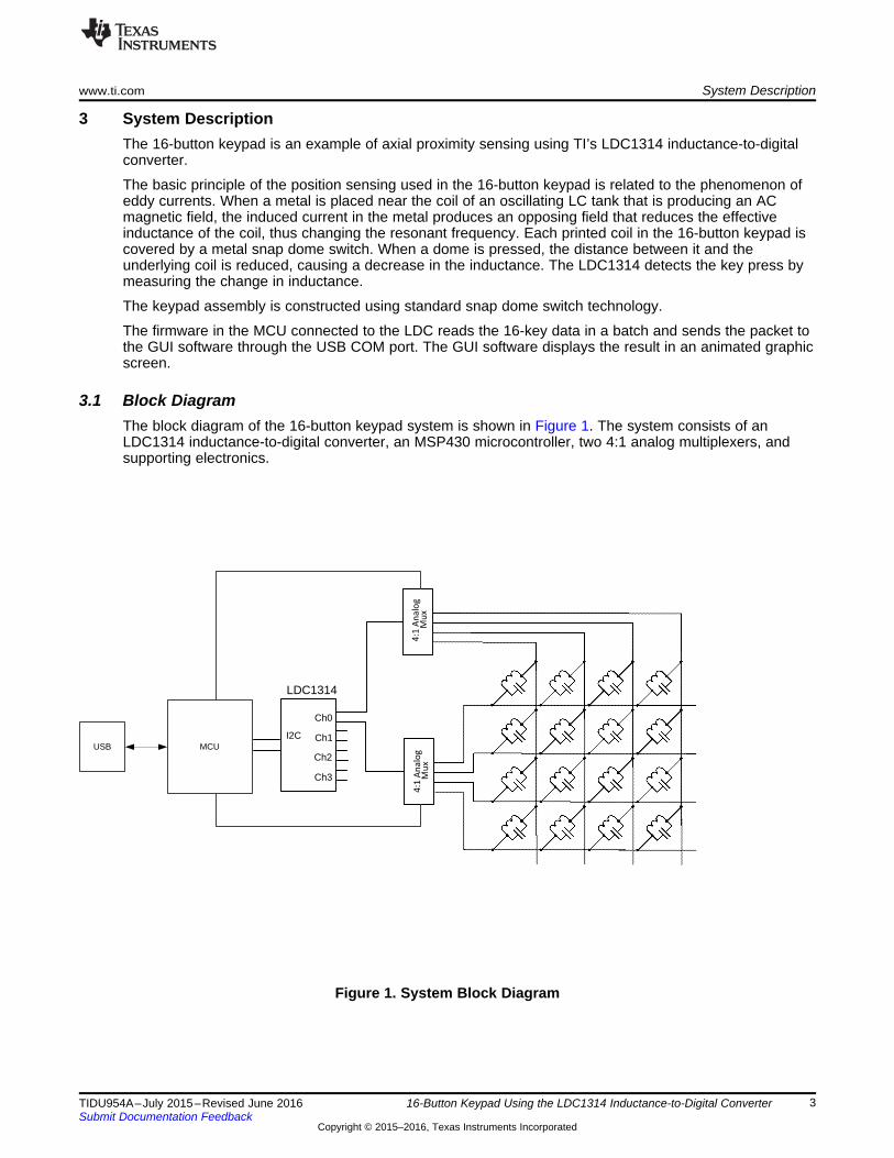
3.1 Block DiagramThe block diagram of the 16-button keypad system is shown in Figure 1. The system consists of anLDC1314 inductance-to-digital converter, an MSP430 microcontroller, two 4:1 analog multiplexers, andsupporting electronics.
16-Button Keypad Using the LDC1314 Inductance-to-Digital Converter
3.2 LDC1314The LDC1314 is a 4-channel inductance-to-digital converter. An internal multiplexer connects the oscillatorto one of the four channels per the register settings. In the keypad demo, only Channel 0 is used. Theconverter is set to the continuous conversion mode. This design can be expanded to 32 or 64 keys byusing the rest of the channels. The internal clock reference source is used in this design, saving the costof an external crystal oscillator.
Figure 2. LDC1314 Functional Block Diagram
3.3 Other TI PartsAn MSP430 microcontroller is used as a bridge between the LDC1314 and the USB port. It also providesthe non-volatile memory for the dial’s calibration data.
An LP2985 low-dropout linear regulator is used to step down the 5-V USB power to the 3.3 V required bythe LDC1314 and the MSP430.
To protect the demo board circuit from possible ESD surge, the demo board uses a TPD4E004, the ESDprotection circuit for high-speed data lines.
16-Button Keypad Using the LDC1314 Inductance-to-Digital Converter
4 System Design Theory: General Guide for Inductive Sensing Using LDC1314
4.1 Working PrinciplesThe working principle of the LDC1314 is based on the phenomenon that occurs when a conductivematerial, such as a metal, is placed in a magnetic field. An alternating current flowing through an inductorwill generate an AC magnetic field. If a conductive material, such as a metal object, is brought into thevicinity of the inductor, the magnetic field will induce a circulating current (eddy current) on the surface ofthe conductor. The eddy current is a function of the distance, size, and composition of the conductor. Theeddy current generates its own magnetic field, which opposes the original field generated by the sensorinductor. This effect is equivalent to a set of coupled inductors, where the sensor inductor is the primarywinding and the eddy current in the target object represents the secondary winding. The coupling betweenthe inductors is a function of the sensor inductor and the resistivity, distance, size, and shape of theconductive target. The resistance and inductance of the secondary winding caused by the eddy currentcan be modeled as distance dependent resistive and inductive components.
In Figure 3(a), an electrical model is shown. The primary side represents the electrical model of a coil withseries resistance (RS), parasitic capacitance (CPAR), and current I1. The secondary side represents thetarget model with eddy current I2. The mutual inductance [M(d)] between the primary and secondary sidesis a function of the distance between the two. Based on the dot convention, the voltage across the primarycoil, VP, is given by Equation 1:
(1)
As the distance between the sensor coil and the target decreases, the mutual inductance M(d) increases,and the magnetic field strength at the surface of the target increases, increasing I2. Because both M and I2increase, the total voltage across the primary side decreases. Looking into the terminals of the primaryside, this appears as a reduction in the effective inductance.
An equivalent, parallel R-L-C model of the sensor and target can be constructed, as shown in Figure 3(b).Both the inductance and resistance vary with the distance between the target and sensor coil. The parallelequivalent circuit becomes a parallel resistor at parallel resonance when the impedance of the parallelinductance is equal to that of the parallel capacitance in value at the parallel resonant frequency.
16-Button Keypad Using the LDC1314 Inductance-to-Digital Converter
The conversions from the series inductance and resistance into their parallel counterpart are listed inTable 1.
Table 1. Converting Series Resonator into Parallel Resonator
SERIES RESONATOR → PARALLEL RESONATORINDUCTANCE LS LP = LS (1 + QS
–2)RESISTANCE RS RP = RS (1 + QS
2)QUALITY FACTOR QS = ωLS / RS QP = RP / ωLP
An EM field can be generated using an L-C resonator, or L-C tank. One topology for an L-C tank is aparallel R-L-C construction, as shown in Figure 3(b). A parallel LC oscillator can be constructed bycombining a frequency selective circuit with a gain block in a closed loop. The criteria for oscillation are:1) loop gain > 1, and 2) closed loop phase shift of 2π radians. In the context of an oscillator, the R-L-Cresonator provides the frequency selectivity and contributes to the phase shift. At resonance, the parallelimpedance of the reactive components (L and C) cancels, leaving only RP, the lossy (resistive) element inthe circuit (Figure 3(c)). L and R are modeled as distance dependent components, and C includes both aparallel capacitance and the parasitic capacitance between the windings of the inductor.
The sensor oscillation frequency FSENSOR is given by:
(2)
Because the effective parallel inductance, LP, decreases as the target moves closer to the sensor coil,Equation 2 tells us that the resonant frequency of the sensor increases.
Various position sensing techniques have been developed based on this phenomenon.
16-Button Keypad Using the LDC1314 Inductance-to-Digital Converter
4.2 Sensor-Target ConfigurationTo design an inductive sensing application, the first step is to convert the measurement goal into theamount of exposure of a metal target in the electromagnetic field generated by the coils. The commonlyused methods include axial proximity and lateral proximity, as depicted in Figure 4. When the metal targetis placed closer to the coil, or more of the metal target overlaps with the coil, more electromagnetic field isintercepted at the target surface. The eddy current increases as more electromagnetic field flux isintercepted, decreasing the effective inductance of the coil that generates the field and increasing the LCtank oscillation frequency. This makes a greater digital output value of the LDC131x or LDC161x.
Figure 4. Commonly Used Sensor-Target Configurations
In some position sensing cases, a single coil is sufficient. Multiple coils can be used to for differential datato cancel certain unwanted changes in the output. In rotational sensing, the use of multiple coils enablescontinuous 360-degree angular position sensing and increases the sensing accuracy.
16-Button Keypad Using the LDC1314 Inductance-to-Digital Converter
4.3 Target Metal and ThicknessCertain metal types perform better than other types, in terms of creating greater sensor output change.These metals are high conductivity, low magnetic permeability metals, including the common aluminum(alloys) and copper (alloys). The 300 series, non-ferritic stainless steel materials (that is, they cannot bepicked up by a magnet) also work well.
Because an alternating current (such as the eddy current) tends to concentrate in the metal surface facingthe sensor coil (known as the "skin effect"), a thin layer of metal usually works well enough. Table 2 showsthe recommended minimum thickness for several commonly used metals, based on the sensor oscillationfrequency.
4.4 Coil Design InformationThe wide range of oscillation frequency and the driving current of the LDC131x and LDC161x gives theuser great flexibility in selecting the dimensions of the coil that best suits their mechanical systemconfiguration. However, certain rules must be followed to ensure the proper operation of the IC.
• LC tank resonant frequency — The recommended sensor frequency range for LDC131x and LDC161xdevices is 1 kHz to 10 MHz
• Inductance of the sensor coil — There is no absolute requirement on the value of the inductance aslong as the range of the resonant frequency and RP (the parallel loss resistance) are not violated.
• Sensor oscillation amplitude — The maximum allowable sensor oscillation amplitude must not exceed1.8 V. The maximum operating amplitude occurs when the target is either at its maximum distancefrom the sensor coil (axial sensing) or the least amount of target area overlaps the coil (lateralsensing). The minimum amplitude occurs when the target is at its closest point to the sensor (axial), orwhen is achieves maximum overlap with the coil (lateral). Maintain the minimum operating amplitudeabove 500 mV. As already explained, the sensor voltage is proportional to RP(d), which will vary as thetarget moves. Therefore, the coil must be carefully designed to maintain a sufficient range of RP overthe operating range to ensure that the sensor oscillation does not collapse.
• RP (Parallel Loss Resistance) of the LC tank — As described in Section 4.1, the LC tank is "lossy" dueto the inductor’s loss and the energy dissipated by the target metal. This loss can be modeled by aparallel equivalent resistance RP. The more the energy loss in the LC tank, the smaller the value of RP.The range of RP values that the LDC131x and LDC161x devices can handle is from 150 Ω to 100 kΩ,with gradually degrading S/N as it decreases below 1 kΩ. Although it is possible for RP to exceed 100kΩ, the minimum RP value is more important in a majority of applications. Higher "open-air" RP (that is,RP value measured with no target metal) helps increase the S/N of the output. To increase the open-airRP, use thick trace size for the printed sensor coil. Appendix A described three methods for measuringRP value of an inductor.
16-Button Keypad Using the LDC1314 Inductance-to-Digital Converter
4.5 Interpreting and Using the Output DataThe digital output of the LDC131x and LDC161x is a number proportional to the LC tank’s oscillatingfrequency:
where• N is 12 for LDC131x and 28 for LDC161x (3)
The tank frequency is monotonically related to the proximity between the sensor coil and the target metal.Since FREF and N are constant, D can be directly used to indicate the target position.
D is a monotonic function of the proximity. In axial sensing, D increases as the distance decreases. Inlateral sensing, D increases as the overlap between the target and the coil increases. In almost all cases,D is not a linear function of the proximity distance.
4.6 Resolution of Position MeasurementThe resolution of a position sensing system is defined as the number of discreet position values that thesensor can resolve within the measurement range. In the LDC131x and LDC161x, the resolution is directlyrelated to how fine the LC tank frequency can be resolved. Suppose the LC tank frequency increases fromF1 to F2 as a result of moving the target from position P1 to P2. The position resolution is then:
where• REFCNT = reference clock count used to measure FTANK (see the LDC1314 datasheet) (4)
Do not confuse this resolution with the number of bits of the output sample. In the case of LDC161x, theoutput samples will always have enough bits to represent the effective resolution shown above. In thecase of LDC131x, because its output samples have only 12 bits, the internally available resolution issometimes under-represented by the output sample, and the effective resolution can decrease. If this isthe case, use the GAIN and OFFSET registers of the LDC1314 to restore the resolution. Altering thereference frequency (including setting the REFDIV register) can also help recover the resolution. The ratioof the effective reference frequency to tank frequency must be greater than 4 for both LDC131x andLDC161x.
4.7 System-to-System Variation and System CalibrationSystem-to-system variations in practical applications do exist. These variations are mainly due to thecomponent tolerances. The capacitance of the capacitors and the inductance of the coils are the maincontributor of the system-to-system variation. Good quality capacitors are recommended, such as theNP0/CG0 ceramic capacitor or film capacitors with a tolerance of 1% to 5%. A non-printed circuit sensorcoil should also have a tolerance of 5% or less.
For sensing systems that require high accuracy, a system calibration will be necessary. Most commoncalibration involves offset and gain calibration. In many systems, on-the-fly calibration is a good choicebecause it does not require permanent calibration data storage.
16-Button Keypad Using the LDC1314 Inductance-to-Digital Converter
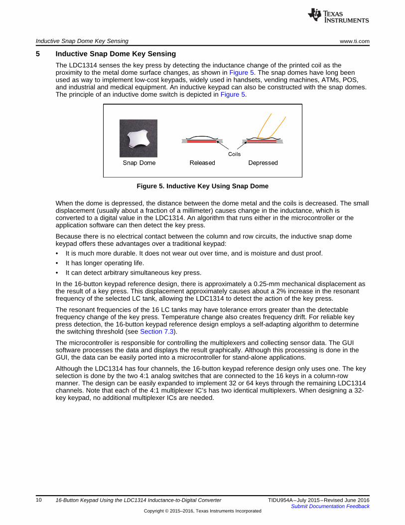
5 Inductive Snap Dome Key SensingThe LDC1314 senses the key press by detecting the inductance change of the printed coil as theproximity to the metal dome surface changes, as shown in Figure 5. The snap domes have long beenused as way to implement low-cost keypads, widely used in handsets, vending machines, ATMs, POS,and industrial and medical equipment. An inductive keypad can also be constructed with the snap domes.The principle of an inductive dome switch is depicted in Figure 5.
Figure 5. Inductive Key Using Snap Dome
When the dome is depressed, the distance between the dome metal and the coils is decreased. The smalldisplacement (usually about a fraction of a millimeter) causes change in the inductance, which isconverted to a digital value in the LDC1314. An algorithm that runs either in the microcontroller or theapplication software can then detect the key press.
Because there is no electrical contact between the column and row circuits, the inductive snap domekeypad offers these advantages over a traditional keypad:• It is much more durable. It does not wear out over time, and is moisture and dust proof.• It has longer operating life.• It can detect arbitrary simultaneous key press.
In the 16-button keypad reference design, there is approximately a 0.25-mm mechanical displacement asthe result of a key press. This displacement approximately causes about a 2% increase in the resonantfrequency of the selected LC tank, allowing the LDC1314 to detect the action of the key press.
The resonant frequencies of the 16 LC tanks may have tolerance errors greater than the detectablefrequency change of the key press. Temperature change also creates frequency drift. For reliable keypress detection, the 16-button keypad reference design employs a self-adapting algorithm to determinethe switching threshold (see Section 7.3).
The microcontroller is responsible for controlling the multiplexers and collecting sensor data. The GUIsoftware processes the data and displays the result graphically. Although this processing is done in theGUI, the data can be easily ported into a microcontroller for stand-alone applications.
Although the LDC1314 has four channels, the 16-button keypad reference design only uses one. The keyselection is done by the two 4:1 analog switches that are connected to the 16 keys in a column-rowmanner. The design can be easily expanded to implement 32 or 64 keys through the remaining LDC1314channels. Note that each of the 4:1 multiplexer IC’s has two identical multiplexers. When designing a 32-key keypad, no additional multiplexer ICs are needed.
16-Button Keypad Using the LDC1314 Inductance-to-Digital Converter
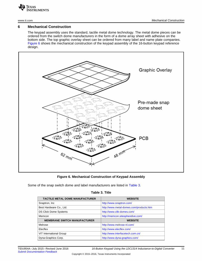
6 Mechanical ConstructionThe keypad assembly uses the standard, tactile metal dome technology. The metal dome pieces can beordered from the switch dome manufacturers in the form of a dome array sheet with adhesive on thebottom side. The top graphic overlay sheet can be ordered from many label and name plate companies.Figure 6 shows the mechanical construction of the keypad assembly of the 16-button keypad referencedesign.
Figure 6. Mechanical Construction of Keypad Assembly
Some of the snap switch dome and label manufacturers are listed in Table 3.
Table 3. Title
TACTILE METAL DOME MANUFACTURER WEBSITESnaptron, Inc http://www.snaptron.com/Best Hardware Co., Ltd. http://www.metal-domes.com/products.htmDS Click Dome Systems http://www.clik-domes.com/Memcon http://memcon.sitespherelive.com/
MEMBRANE SWITCH MANUFACTURER WEBSITEMelrose http://www.melrose-nl.com/Elecflex http://www.elecflex.com/VIT International Group http://www.interfacetech.com.cn/Dyna-Graphics Corp. http://www.dyna-graphics.com/
16-Button Keypad Using the LDC1314 Inductance-to-Digital Converter
7 Hardware DesignThe LDC1314 uses an inductor as the sensor. It excites the LC tank circuit, senses the proximity betweenthe sensor and target metal by measuring the oscillating frequency. In the 16-button keypad referencedesign, there is a coil for each snap dome. The coils are printed in the inner two layers of a four-layerPCB, providing maximum protection from wear and tear and external environment. A center hole isfabricated in the middle of each coil that provides an air passage to ensure free movement of the domeunder the sealed top graphic membrane.
7.1 Sensor DesignThe diameter of the each coil is 8 mm, matching the size of the snap dome. The nominal inductance ofthe coil is around 2.3 μH. Each coil contains 16 turns on each side. The tank capacitor value is 150 pF.The average resonance frequency is around 9.5 MHz after the keypad is assembled. The 43-MHz internalreference oscillator of the LDC1314 is used, saving the cost of an external crystal oscillator.
The keypad PCB and graphic overlay designs are shown in Figure 7.
16-Button Keypad Using the LDC1314 Inductance-to-Digital Converter
7.2 Scan LoopThe scan loop is driven by the GUI software, which requests the microcontroller to send the data for the16 keys in a block. The data is then processed to identify the key presses and the result is displayed onthe GUI screen. Figure 8 illustrates the scan loop flowchart.
Figure 8. Key Scan Loop
7.3 Key Press IdentificationAs mentioned in Section 5, a self-adapting algorithm is used in the 16-button keypad reference design toreliably detect the key presses. This is done in the GUI software. The algorithm keeps an array of the"unpressed" values, referred to as the "base value", of each key by slowly tracking the change of the keyvalues. The "slow tracking" is done by incrementing the base value when the most recent key data isgreater than the base value, and decrementing the base value if the most recent key data is smaller thanthe current value. With this action, fast changes (from a key press, for example) are effectively ignored.The base value is kept unchanged otherwise. The slow changes, such as those due to temperature drift,are tracked continuously. A fixed threshold above the base value is used to judge if the key is depressed.The self-adapting algorithm is shown in Figure 9.
16-Button Keypad Using the LDC1314 Inductance-to-Digital Converter
8 Firmware
8.1 Com Port CommandsThe MSP430 firmware of the keypad bridges between the I2C interface of the LDC1314 and the virtualCOM port of the GUI. The baud rate is 912.6k. There are seven commands:• RK n: This command requests the firmware to send the sensor output data, each 16 bits long, in the
following sequence: Ch0, Ch1, Ch2, Ch3• FB n: Set flash block• BW w w: Block-writes the 16-bit values that follow to the flash storage of the MCU, starting from
address 0• BR n: Requests the firmware to send n 16-bits values in the flash storage from address 0• IW addr reg w: Writes the 16-bit value w into the reg register of the I2C device having address addr• IR addr reg: Requests the firmware to send the 16-bit content of register reg of the I2C device having
address addr• LR: Loads the default register values into the LDC1314 registers (with an I2C address of 2 A)
8.2 Flash Storage Data FormatThe flash memory dedicated to the keypad firmware has the following assignment:
16-Button Keypad Using the LDC1314 Inductance-to-Digital Converter
Upon power up, these values are written into the intended LDC1314 registers. The LDC1314 registers canalso be reloaded by the LR command. The actual register contents are shown in Table 4.
16-Button Keypad Using the LDC1314 Inductance-to-Digital Converter
8.3 Application Specific CommandThe RK command is designed specifically for this inductive keypad. It handles the multiplexing andreading of the data from the 16 keys and transmits it to the GUI. To ensure reliable reading of the correctkey values, certain timing requirement must be observed, as shown in Figure 10.
Figure 10. Timing Requirement for a Single Key Read
16-Button Keypad Using the LDC1314 Inductance-to-Digital Converter
9 GUI SoftwareThe GUI software is written in Visual Basic® 2012. The main screen is the graphic animation of thekeypad. Use the USB tab select the COM port used to communicate with the keypad.
9.1 Main ScreenThe main screen is shown in Figure 12 with the pressed keys highlighted.
Figure 12. Main Screen
9.2 USB ScreenThe COM port is selected in the USB screen. The COM port must be first selected for the properoperation of the 16-button keypad. The USB screen is shown in Figure 13.
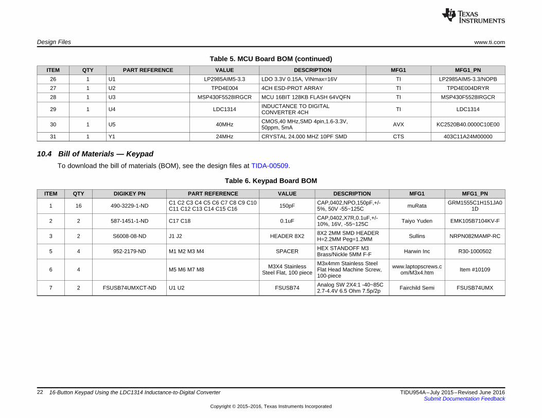
8 1 C11 0.47u CAP CER .47UF 25V X7R 0603 muRata GRM188R71E474KA12D9 1 D1 MMSZ5232 ZENER 5.6V 500mW Diodes MMSZ5232B-7-F10 1 D2 LED Green LED Diffused Green High Efficinecy Osram LG L29K-G2J1-24-Z
11 1 D3 RED LED LED 660NM SUPER RED DIFF0603SMD Lumex SML-LX0603SRW-TR
16-Button Keypad Using the LDC1314 Inductance-to-Digital Converter
10.5 Layer PlotsThe LDC1314 has a nominal minimum requirement of 2.3 µH for coil inductance. This inductance can beachieved by a 2-layer coil with a 8-mm diameter using 4-mil trace and spacing. The composite view ofPCB layout image is shown in Figure 16. The coils are printed in the layer 2 and 3 of the 4-layer board.
To download the layer plots, see the design files at TIDA-00509.
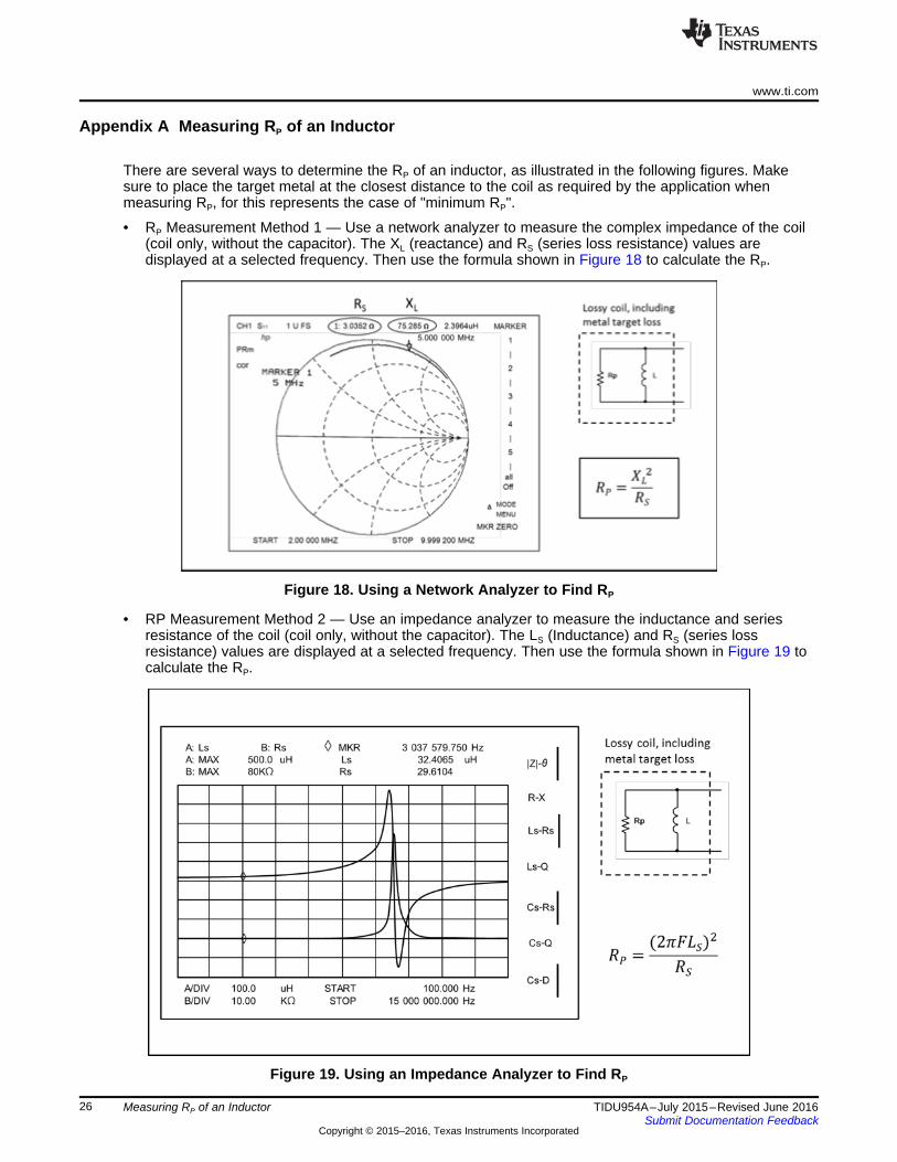
There are several ways to determine the RP of an inductor, as illustrated in the following figures. Makesure to place the target metal at the closest distance to the coil as required by the application whenmeasuring RP, for this represents the case of "minimum RP".
• RP Measurement Method 1 — Use a network analyzer to measure the complex impedance of the coil(coil only, without the capacitor). The XL (reactance) and RS (series loss resistance) values aredisplayed at a selected frequency. Then use the formula shown in Figure 18 to calculate the RP.
Figure 18. Using a Network Analyzer to Find RP
• RP Measurement Method 2 — Use an impedance analyzer to measure the inductance and seriesresistance of the coil (coil only, without the capacitor). The LS (Inductance) and RS (series lossresistance) values are displayed at a selected frequency. Then use the formula shown in Figure 19 tocalculate the RP.
Revision A HistoryNOTE: Page numbers for previous revisions may differ from page numbers in the current version.
Changes from Original (July 2015) to A Revision ........................................................................................................... Page
• Changed Equation 2 content from "LPC" to "LP × C"................................................................................. 6
Texas Instruments Incorporated (‘TI”) reference designs are solely intended to assist designers (“Designer(s)”) who are developing systemsthat incorporate TI products. TI has not conducted any testing other than that specifically described in the published documentation for aparticular reference design.TI’s provision of reference designs and any other technical, applications or design advice, quality characterization, reliability data or otherinformation or services does not expand or otherwise alter TI’s applicable published warranties or warranty disclaimers for TI products, andno additional obligations or liabilities arise from TI providing such reference designs or other items.TI reserves the right to make corrections, enhancements, improvements and other changes to its reference designs and other items.Designer understands and agrees that Designer remains responsible for using its independent analysis, evaluation and judgment indesigning Designer’s systems and products, and has full and exclusive responsibility to assure the safety of its products and compliance ofits products (and of all TI products used in or for such Designer’s products) with all applicable regulations, laws and other applicablerequirements. Designer represents that, with respect to its applications, it has all the necessary expertise to create and implementsafeguards that (1) anticipate dangerous consequences of failures, (2) monitor failures and their consequences, and (3) lessen thelikelihood of failures that might cause harm and take appropriate actions. Designer agrees that prior to using or distributing any systemsthat include TI products, Designer will thoroughly test such systems and the functionality of such TI products as used in such systems.Designer may not use any TI products in life-critical medical equipment unless authorized officers of the parties have executed a specialcontract specifically governing such use. Life-critical medical equipment is medical equipment where failure of such equipment would causeserious bodily injury or death (e.g., life support, pacemakers, defibrillators, heart pumps, neurostimulators, and implantables). Suchequipment includes, without limitation, all medical devices identified by the U.S. Food and Drug Administration as Class III devices andequivalent classifications outside the U.S.Designers are authorized to use, copy and modify any individual TI reference design only in connection with the development of endproducts that include the TI product(s) identified in that reference design. HOWEVER, NO OTHER LICENSE, EXPRESS OR IMPLIED, BYESTOPPEL OR OTHERWISE TO ANY OTHER TI INTELLECTUAL PROPERTY RIGHT, AND NO LICENSE TO ANY TECHNOLOGY ORINTELLECTUAL PROPERTY RIGHT OF TI OR ANY THIRD PARTY IS GRANTED HEREIN, including but not limited to any patent right,copyright, mask work right, or other intellectual property right relating to any combination, machine, or process in which TI products orservices are used. Information published by TI regarding third-party products or services does not constitute a license to use such productsor services, or a warranty or endorsement thereof. Use of the reference design or other items described above may require a license from athird party under the patents or other intellectual property of the third party, or a license from TI under the patents or other intellectualproperty of TI.TI REFERENCE DESIGNS AND OTHER ITEMS DESCRIBED ABOVE ARE PROVIDED “AS IS” AND WITH ALL FAULTS. TI DISCLAIMSALL OTHER WARRANTIES OR REPRESENTATIONS, EXPRESS OR IMPLIED, REGARDING THE REFERENCE DESIGNS OR USE OFTHE REFERENCE DESIGNS, INCLUDING BUT NOT LIMITED TO ACCURACY OR COMPLETENESS, TITLE, ANY EPIDEMIC FAILUREWARRANTY AND ANY IMPLIED WARRANTIES OF MERCHANTABILITY, FITNESS FOR A PARTICULAR PURPOSE, AND NON-INFRINGEMENT OF ANY THIRD PARTY INTELLECTUAL PROPERTY RIGHTS.TI SHALL NOT BE LIABLE FOR AND SHALL NOT DEFEND OR INDEMNIFY DESIGNERS AGAINST ANY CLAIM, INCLUDING BUT NOTLIMITED TO ANY INFRINGEMENT CLAIM THAT RELATES TO OR IS BASED ON ANY COMBINATION OF PRODUCTS ASDESCRIBED IN A TI REFERENCE DESIGN OR OTHERWISE. IN NO EVENT SHALL TI BE LIABLE FOR ANY ACTUAL, DIRECT,SPECIAL, COLLATERAL, INDIRECT, PUNITIVE, INCIDENTAL, CONSEQUENTIAL OR EXEMPLARY DAMAGES IN CONNECTION WITHOR ARISING OUT OF THE REFERENCE DESIGNS OR USE OF THE REFERENCE DESIGNS, AND REGARDLESS OF WHETHER TIHAS BEEN ADVISED OF THE POSSIBILITY OF SUCH DAMAGES.TI’s standard terms of sale for semiconductor products (http://www.ti.com/sc/docs/stdterms.htm) apply to the sale of packaged integratedcircuit products. Additional terms may apply to the use or sale of other types of TI products and services.Designer will fully indemnify TI and its representatives against any damages, costs, losses, and/or liabilities arising out of Designer’s non-compliance with the terms and provisions of this Notice.IMPORTANT NOTICE