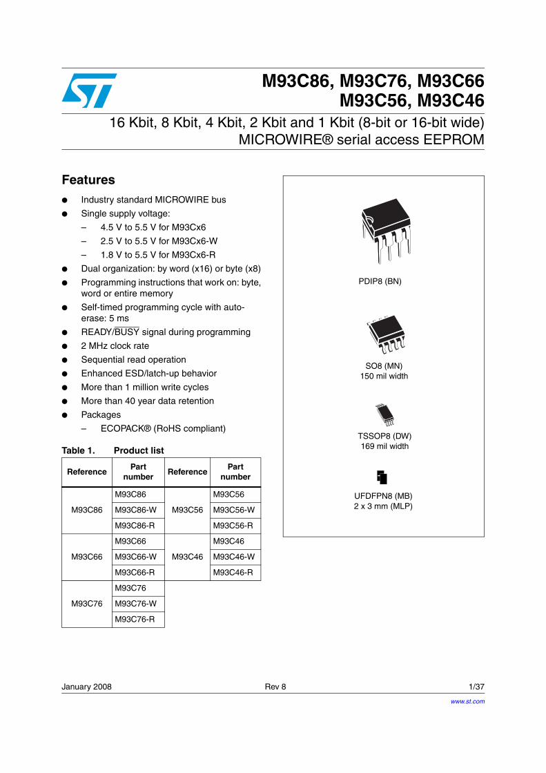
January 2008 Rev 8 1/37 1 M93C86, M93C76, M93C66 M93C56, M93C46 16 Kbit, 8 Kbit, 4 Kbit, 2 Kbit and 1 Kbit (8-bit or 16-bit wide) MICROWIRE® serial access EEPROM Features ● Industry standard MICROWIRE bus ● Single supply voltage: – 4.5 V to 5.5 V for M93Cx6 – 2.5 V to 5.5 V for M93Cx6-W – 1.8 V to 5.5 V for M93Cx6-R ● Dual organization: by word (x16) or byte (x8) ● Programming instructions that work on: byte, word or entire memory ● Self-timed programming cycle with auto- erase: 5 ms ● READY/BUSY signal during programming ● 2 MHz clock rate ● Sequential read operation ● Enhanced ESD/latch-up behavior ● More than 1 million write cycles ● More than 40 year data retention ● Packages – ECOPACK® (RoHS compliant) Table 1. Product list Reference Part number Reference Part number M93C86 M93C86 M93C56 M93C56 M93C86-W M93C56-W M93C86-R M93C56-R M93C66 M93C66 M93C46 M93C46 M93C66-W M93C46-W M93C66-R M93C46-R M93C76 M93C76 M93C76-W M93C76-R PDIP8 (BN) SO8 (MN) 150 mil width TSSOP8 (DW) 169 mil width UFDFPN8 (MB) 2 x 3 mm (MLP) www.st.com
Transcript
January 2008 Rev 8 1/37
1
M93C86, M93C76, M93C66M93C56, M93C46
16 Kbit, 8 Kbit, 4 Kbit, 2 Kbit and 1 Kbit (8-bit or 16-bit wide)MICROWIRE® serial access EEPROM
Features Industry standard MICROWIRE bus
Single supply voltage:
– 4.5 V to 5.5 V for M93Cx6
– 2.5 V to 5.5 V for M93Cx6-W
– 1.8 V to 5.5 V for M93Cx6-R
Dual organization: by word (x16) or byte (x8)
Programming instructions that work on: byte, word or entire memory
Self-timed programming cycle with auto-erase: 5 ms
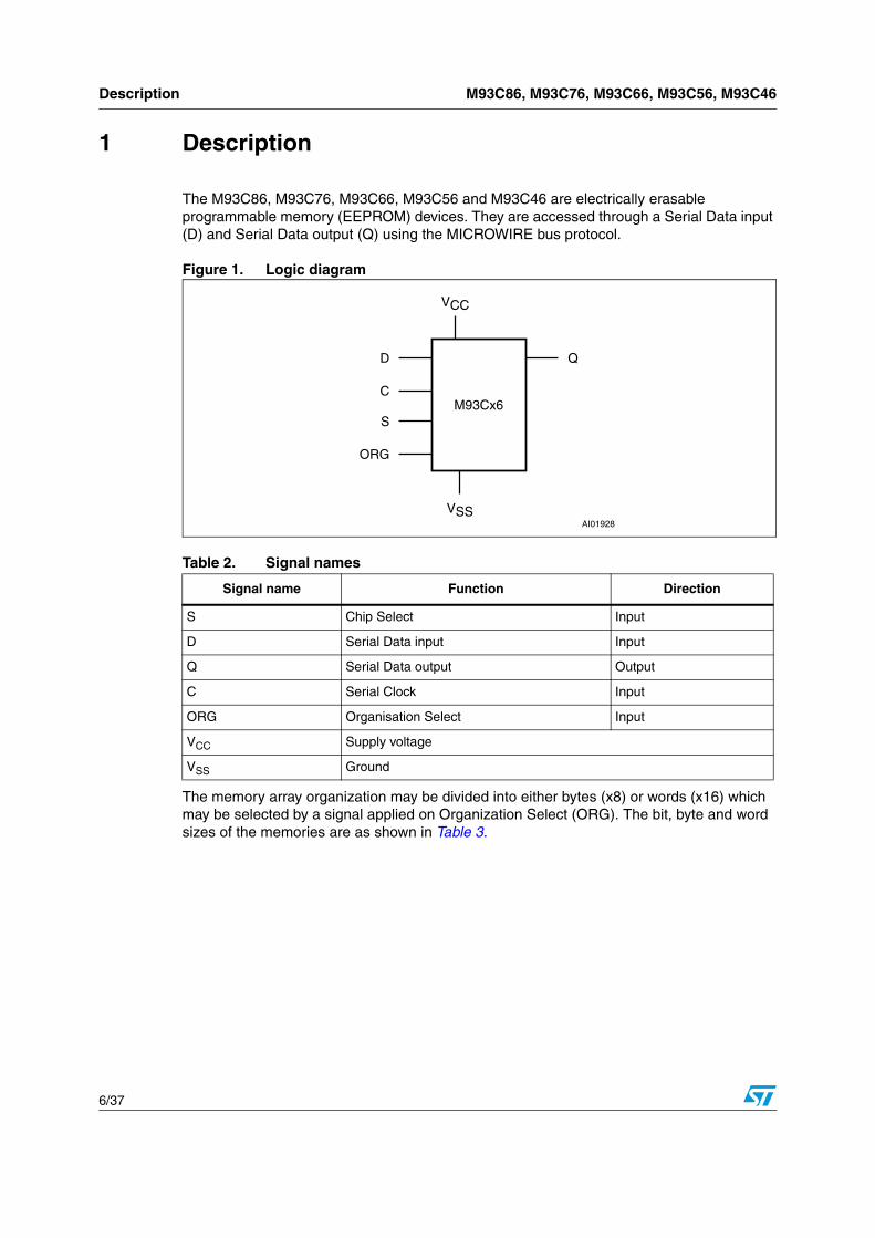
The M93C86, M93C76, M93C66, M93C56 and M93C46 are electrically erasable programmable memory (EEPROM) devices. They are accessed through a Serial Data input (D) and Serial Data output (Q) using the MICROWIRE bus protocol.
Figure 1. Logic diagram
The memory array organization may be divided into either bytes (x8) or words (x16) which may be selected by a signal applied on Organization Select (ORG). The bit, byte and word sizes of the memories are as shown in Table 3.
The M93Cx6 is accessed by a set of instructions, as summarized in Table 4., and in more detail in Table 5. to Table 7.).
A Read Data from Memory (READ) instruction loads the address of the first byte or word to be read in an internal address register. The data at this address is then clocked out serially. The address register is automatically incremented after the data is output and, if Chip Select Input (S) is held High, the M93Cx6 can output a sequential stream of data bytes or words. In this way, the memory can be read as a data stream from eight to 16384 bits long (in the case of the M93C86), or continuously (the address counter automatically rolls over to 00h when the highest address is reached).
Programming is internally self-timed (the external clock signal on Serial Clock (C) may be stopped or left running after the start of a Write cycle) and does not require an Erase cycle prior to the Write instruction. The Write instruction writes 8 or 16 bits at a time into one of the byte or word locations of the M93Cx6. After the start of the programming cycle, a Busy/Ready signal is available on Serial Data Output (Q) when Chip Select Input (S) is driven High.
An internal Power-on Data Protection mechanism in the M93Cx6 inhibits the device when the supply is too low.
Table 3. Memory size versus organization
Device Number of bits Number of 8-bit bytes Number of 16-bit words
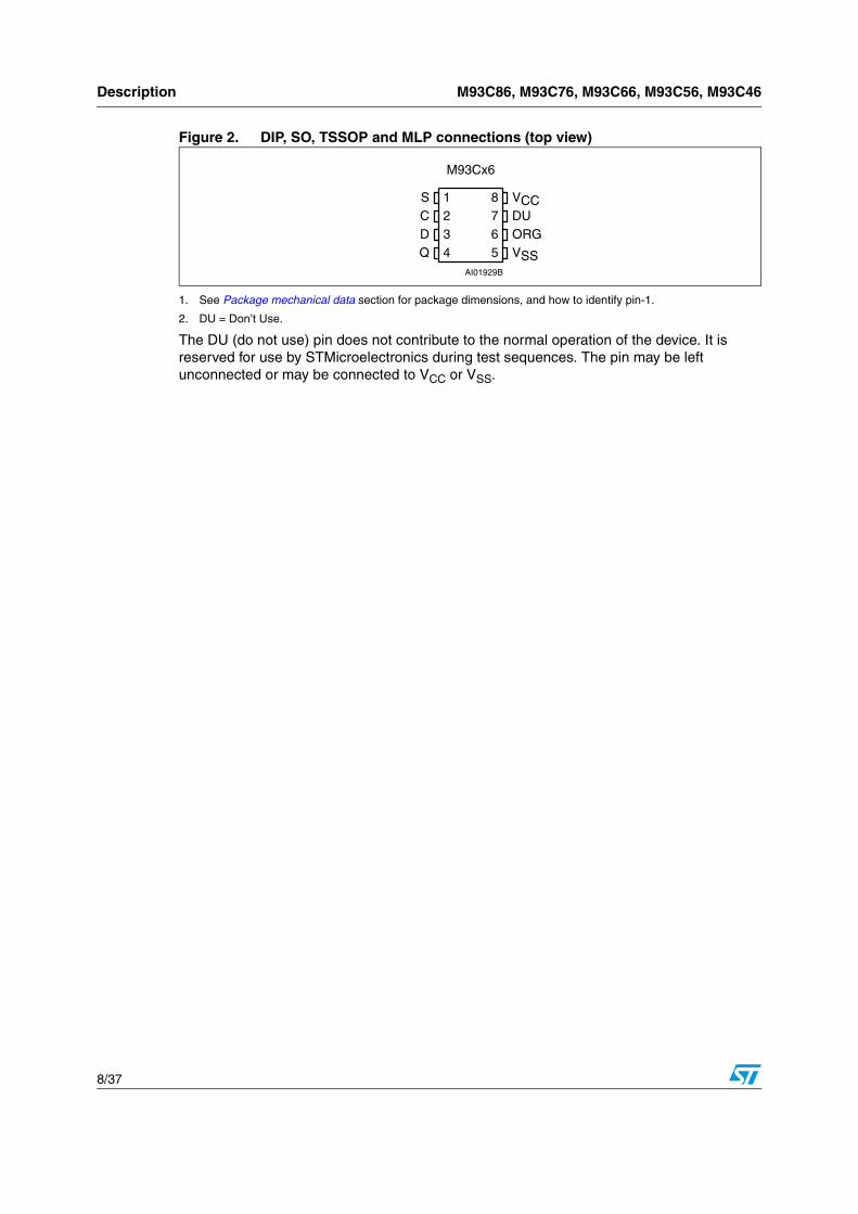
Figure 2. DIP, SO, TSSOP and MLP connections (top view)
1. See Package mechanical data section for package dimensions, and how to identify pin-1.
2. DU = Don’t Use.
The DU (do not use) pin does not contribute to the normal operation of the device. It is reserved for use by STMicroelectronics during test sequences. The pin may be left unconnected or may be connected to VCC or VSS.
VSSQORGDUC
S VCC
D
AI01929B
M93Cx6
1234
8765
M93C86, M93C76, M93C66, M93C56, M93C46 Connecting to the serial bus
9/37
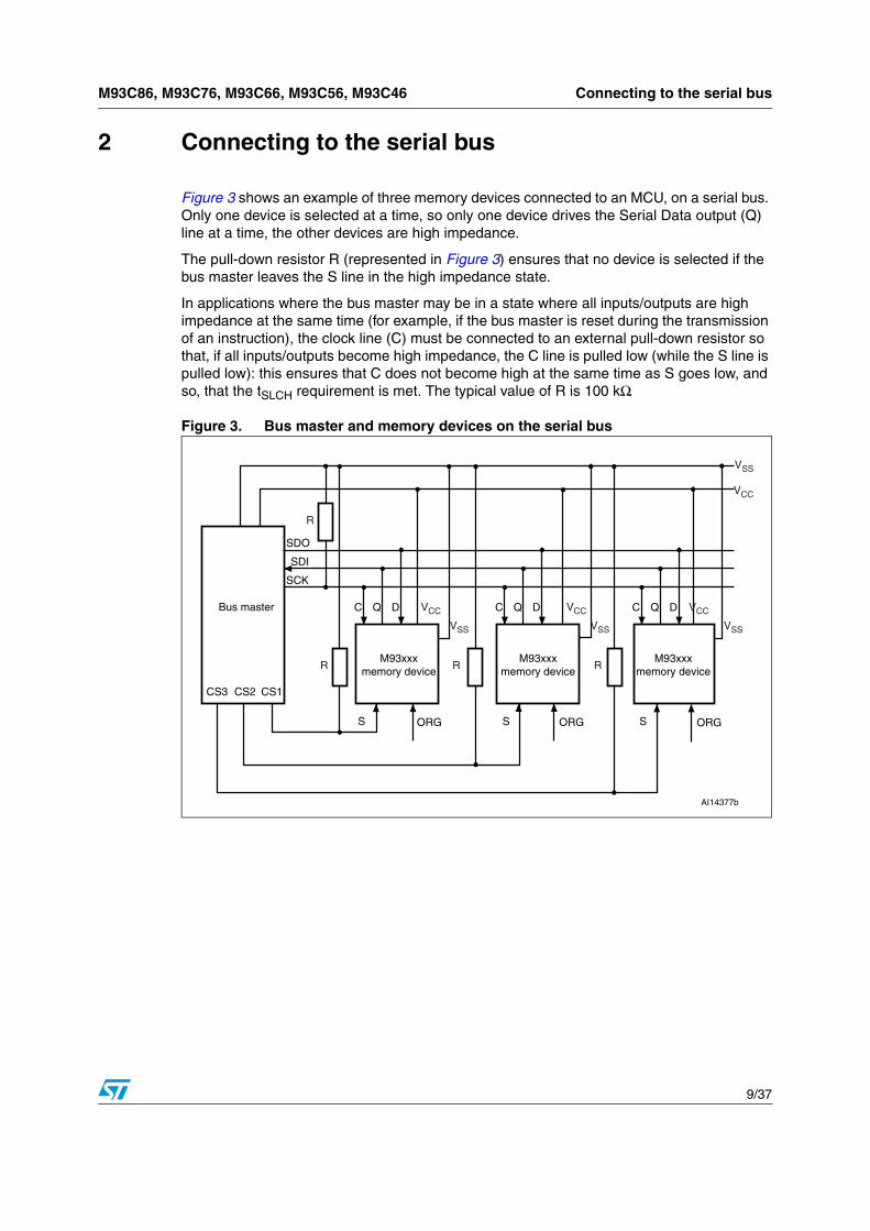
2 Connecting to the serial bus
Figure 3 shows an example of three memory devices connected to an MCU, on a serial bus. Only one device is selected at a time, so only one device drives the Serial Data output (Q) line at a time, the other devices are high impedance.
The pull-down resistor R (represented in Figure 3) ensures that no device is selected if the bus master leaves the S line in the high impedance state.
In applications where the bus master may be in a state where all inputs/outputs are high impedance at the same time (for example, if the bus master is reset during the transmission of an instruction), the clock line (C) must be connected to an external pull-down resistor so that, if all inputs/outputs become high impedance, the C line is pulled low (while the S line is pulled low): this ensures that C does not become high at the same time as S goes low, and so, that the tSLCH requirement is met. The typical value of R is 100 kΩ.
Figure 3. Bus master and memory devices on the serial bus
AI14377b
Bus master
M93xxxmemory device
SDO
SDI
SCK
C Q D
S
M93xxxmemory device
C Q D
S
M93xxxmemory device
C Q D
S
CS3 CS2 CS1
ORG ORG ORG
R R R
VCC
VCC VCC VCC
VSS
VSS VSS VSS
R
Operating features M93C86, M93C76, M93C66, M93C56, M93C46
10/37
3 Operating features
3.1 Supply voltage (VCC)
3.1.1 Operating supply voltage VCC
Prior to selecting the memory and issuing instructions to it, a valid and stable VCC voltage within the specified [VCC(min), VCC(max)] range must be applied. In order to secure a stable DC supply voltage, it is recommended to decouple the VCC line with a suitable capacitor (usually of the order of 10 nF to 100 nF) close to the VCC/VSS package pins.
This voltage must remain stable and valid until the end of the transmission of the instruction and, for a Write instruction, until the completion of the internal write cycle (tW).
3.1.2 Power-up conditions
When the power supply is turned on, VCC rises from VSS to VCC. During this time, the Chip Select (S) line is not allowed to float and should be driven to VSS, it is therefore recommended to connect the S line to VSS via a suitable pull-down resistor.
The VCC rise time must not vary faster than 1 V/µs.
3.1.3 Power-up and device reset
In order to prevent inadvertent Write operations during power-up, a power on reset (POR) circuit is included. At power-up (continuous rise of VCC), the device does not respond to any instruction until VCC has reached the power on reset threshold voltage (this threshold is lower than the minimum VCC operating voltage defined in Table 9, Table 10 and Table 11).
When VCC passes the POR threshold, the device is reset and is in the following state:
Standby Power mode
deselected (assuming that there is a pull-down resistor on the S line)
3.1.4 Power-down
At power-down (continuous decrease in VCC), as soon as VCC drops from the normal operating voltage to below the power on reset threshold voltage, the device stops responding to any instruction sent to it.
During power-down, the device must be deselected and in the Standby Power mode (that is, there should be no internal Write cycle in progress).
The M93Cx6 memory is organized either as bytes (x8) or as words (x16). If Organization Select (ORG) is left unconnected (or connected to VCC) the x16 organization is selected; when Organization Select (ORG) is connected to Ground (VSS) the x8 organization is selected. When the M93Cx6 is in Standby mode, Organization Select (ORG) should be set either to VSS or VCC for minimum power consumption. Any voltage between VSS and VCC applied to Organization Select (ORG) may increase the Standby current.
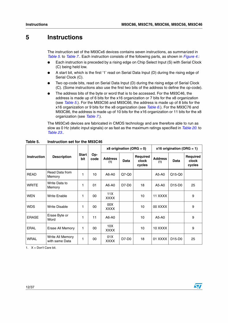
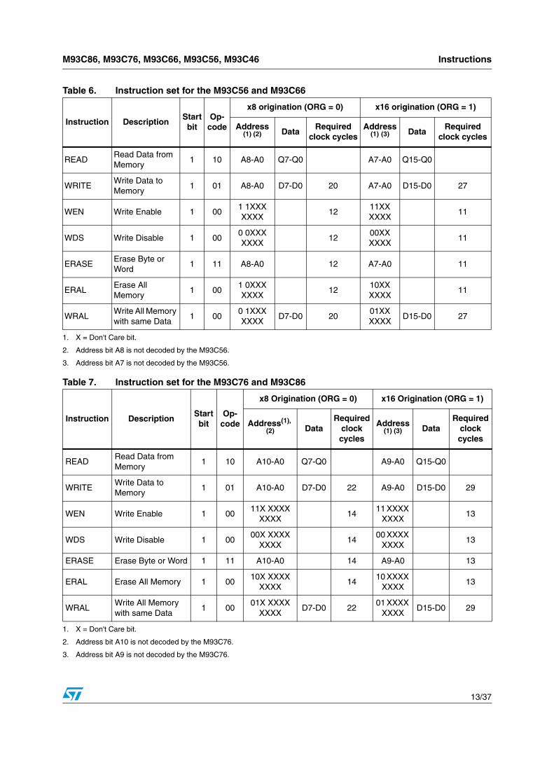
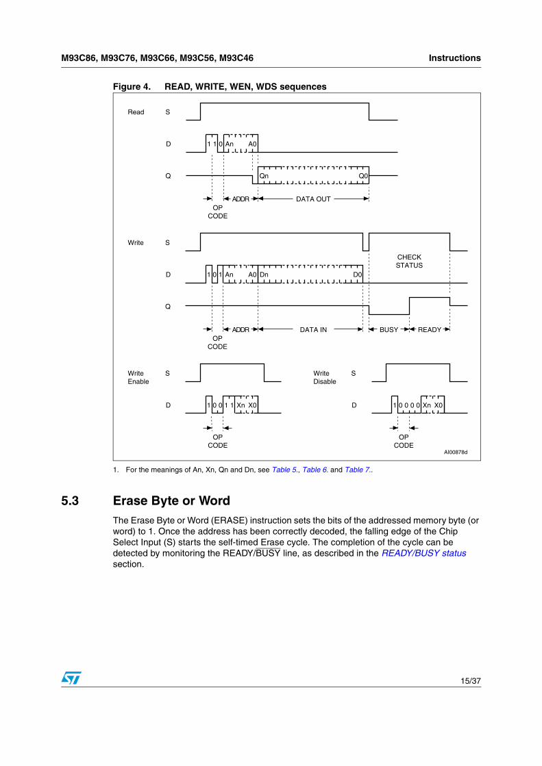
The instruction set of the M93Cx6 devices contains seven instructions, as summarized in Table 5. to Table 7.. Each instruction consists of the following parts, as shown in Figure 4.:
Each instruction is preceded by a rising edge on Chip Select Input (S) with Serial Clock (C) being held low.
A start bit, which is the first ‘1’ read on Serial Data Input (D) during the rising edge of Serial Clock (C).
Two op-code bits, read on Serial Data Input (D) during the rising edge of Serial Clock (C). (Some instructions also use the first two bits of the address to define the op-code).
The address bits of the byte or word that is to be accessed. For the M93C46, the address is made up of 6 bits for the x16 organization or 7 bits for the x8 organization (see Table 5.). For the M93C56 and M93C66, the address is made up of 8 bits for the x16 organization or 9 bits for the x8 organization (see Table 6.). For the M93C76 and M93C86, the address is made up of 10 bits for the x16 organization or 11 bits for the x8 organization (see Table 7.).
The M93Cx6 devices are fabricated in CMOS technology and are therefore able to run as slow as 0 Hz (static input signals) or as fast as the maximum ratings specified in Table 20. to Table 23..
5.1 Read Data from MemoryThe Read Data from Memory (READ) instruction outputs data on Serial Data Output (Q). When the instruction is received, the op-code and address are decoded, and the data from the memory is transferred to an output shift register. A dummy 0 bit is output first, followed by the 8-bit byte or 16-bit word, with the most significant bit first. Output data changes are triggered by the rising edge of Serial Clock (C). The M93Cx6 automatically increments the internal address register and clocks out the next byte (or word) as long as the Chip Select Input (S) is held High. In this case, the dummy 0 bit is not output between bytes (or words) and a continuous stream of data can be read.
5.2 Write Enable and Write DisableThe Write Enable (WEN) instruction enables the future execution of erase or write instructions, and the Write Disable (WDS) instruction disables it. When power is first applied, the M93Cx6 initializes itself so that erase and write instructions are disabled. After an Write Enable (WEN) instruction has been executed, erasing and writing remains enabled until an Write Disable (WDS) instruction is executed, or until VCC falls below the power-on reset threshold voltage. To protect the memory contents from accidental corruption, it is advisable to issue the Write Disable (WDS) instruction after every write cycle. The Read Data from Memory (READ) instruction is not affected by the Write Enable (WEN) or Write Disable (WDS) instructions.
1. For the meanings of An, Xn, Qn and Dn, see Table 5., Table 6. and Table 7..
5.3 Erase Byte or WordThe Erase Byte or Word (ERASE) instruction sets the bits of the addressed memory byte (or word) to 1. Once the address has been correctly decoded, the falling edge of the Chip Select Input (S) starts the self-timed Erase cycle. The completion of the cycle can be detected by monitoring the READY/BUSY line, as described in the READY/BUSY status section.
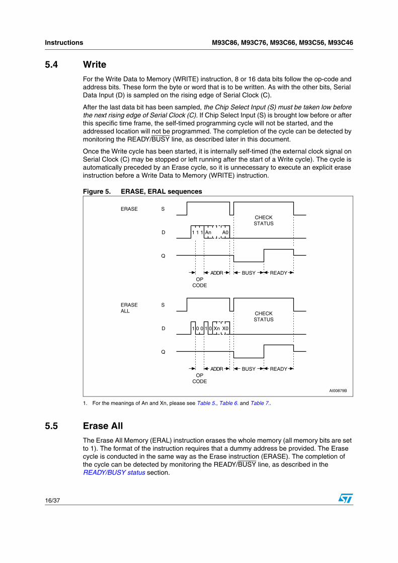
5.4 WriteFor the Write Data to Memory (WRITE) instruction, 8 or 16 data bits follow the op-code and address bits. These form the byte or word that is to be written. As with the other bits, Serial Data Input (D) is sampled on the rising edge of Serial Clock (C).
After the last data bit has been sampled, the Chip Select Input (S) must be taken low before the next rising edge of Serial Clock (C). If Chip Select Input (S) is brought low before or after this specific time frame, the self-timed programming cycle will not be started, and the addressed location will not be programmed. The completion of the cycle can be detected by monitoring the READY/BUSY line, as described later in this document.
Once the Write cycle has been started, it is internally self-timed (the external clock signal on Serial Clock (C) may be stopped or left running after the start of a Write cycle). The cycle is automatically preceded by an Erase cycle, so it is unnecessary to execute an explicit erase instruction before a Write Data to Memory (WRITE) instruction.
Figure 5. ERASE, ERAL sequences
1. For the meanings of An and Xn, please see Table 5., Table 6. and Table 7..
5.5 Erase AllThe Erase All Memory (ERAL) instruction erases the whole memory (all memory bits are set to 1). The format of the instruction requires that a dummy address be provided. The Erase cycle is conducted in the same way as the Erase instruction (ERASE). The completion of the cycle can be detected by monitoring the READY/BUSY line, as described in the READY/BUSY status section.
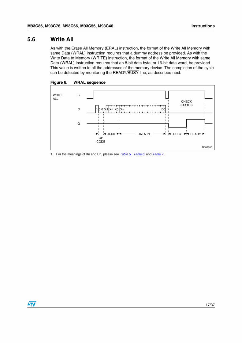
5.6 Write AllAs with the Erase All Memory (ERAL) instruction, the format of the Write All Memory with same Data (WRAL) instruction requires that a dummy address be provided. As with the Write Data to Memory (WRITE) instruction, the format of the Write All Memory with same Data (WRAL) instruction requires that an 8-bit data byte, or 16-bit data word, be provided. This value is written to all the addresses of the memory device. The completion of the cycle can be detected by monitoring the READY/BUSY line, as described next.
Figure 6. WRAL sequence
1. For the meanings of Xn and Dn, please see Table 5., Table 6. and Table 7..
AI00880C
SWRITEALL
DATA IN
D
Q
ADDROP
CODE
Dn D0
BUSY READY
CHECKSTATUS
1 0 00 1 Xn X0
READY/BUSY status M93C86, M93C76, M93C66, M93C56, M93C46
18/37
6 READY/BUSY status
While the Write or Erase cycle is underway, for a WRITE, ERASE, WRAL or ERAL instruction, the Busy signal (Q=0) is returned whenever Chip Select input (S) is driven high. (Please note, though, that there is an initial delay, of tSLSH, before this status information becomes available). In this state, the M93Cx6 ignores any data on the bus. When the Write cycle is completed, and Chip Select Input (S) is driven high, the Ready signal (Q=1) indicates that the M93Cx6 is ready to receive the next instruction. Serial Data Output (Q) remains set to 1 until the Chip Select Input (S) is brought low or until a new start bit is decoded.
7 Initial delivery state
The device is delivered with all bits in the memory array set to 1 (each byte contains FFh).
8 Common I/O operation
Serial Data Output (Q) and Serial Data Input (D) can be connected together, through a current limiting resistor, to form a common, single-wire data bus. Some precautions must be taken when operating the memory in this way, mostly to prevent a short circuit current from flowing when the last address bit (A0) clashes with the first data bit on Serial Data Output (Q). Please see the application note AN394 for details.
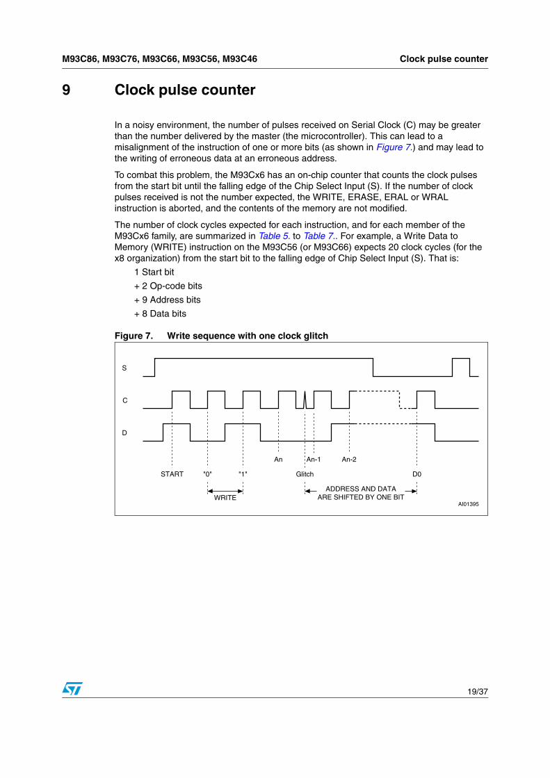
In a noisy environment, the number of pulses received on Serial Clock (C) may be greater than the number delivered by the master (the microcontroller). This can lead to a misalignment of the instruction of one or more bits (as shown in Figure 7.) and may lead to the writing of erroneous data at an erroneous address.
To combat this problem, the M93Cx6 has an on-chip counter that counts the clock pulses from the start bit until the falling edge of the Chip Select Input (S). If the number of clock pulses received is not the number expected, the WRITE, ERASE, ERAL or WRAL instruction is aborted, and the contents of the memory are not modified.
The number of clock cycles expected for each instruction, and for each member of the M93Cx6 family, are summarized in Table 5. to Table 7.. For example, a Write Data to Memory (WRITE) instruction on the M93C56 (or M93C66) expects 20 clock cycles (for the x8 organization) from the start bit to the falling edge of Chip Select Input (S). That is:
1 Start bit
+ 2 Op-code bits
+ 9 Address bits
+ 8 Data bits
Figure 7. Write sequence with one clock glitch
AI01395
S
An-1
C
D
WRITE
START D0"1""0"
An
Glitch
An-2
ADDRESS AND DATAARE SHIFTED BY ONE BIT
Maximum rating M93C86, M93C76, M93C66, M93C56, M93C46
20/37
10 Maximum rating
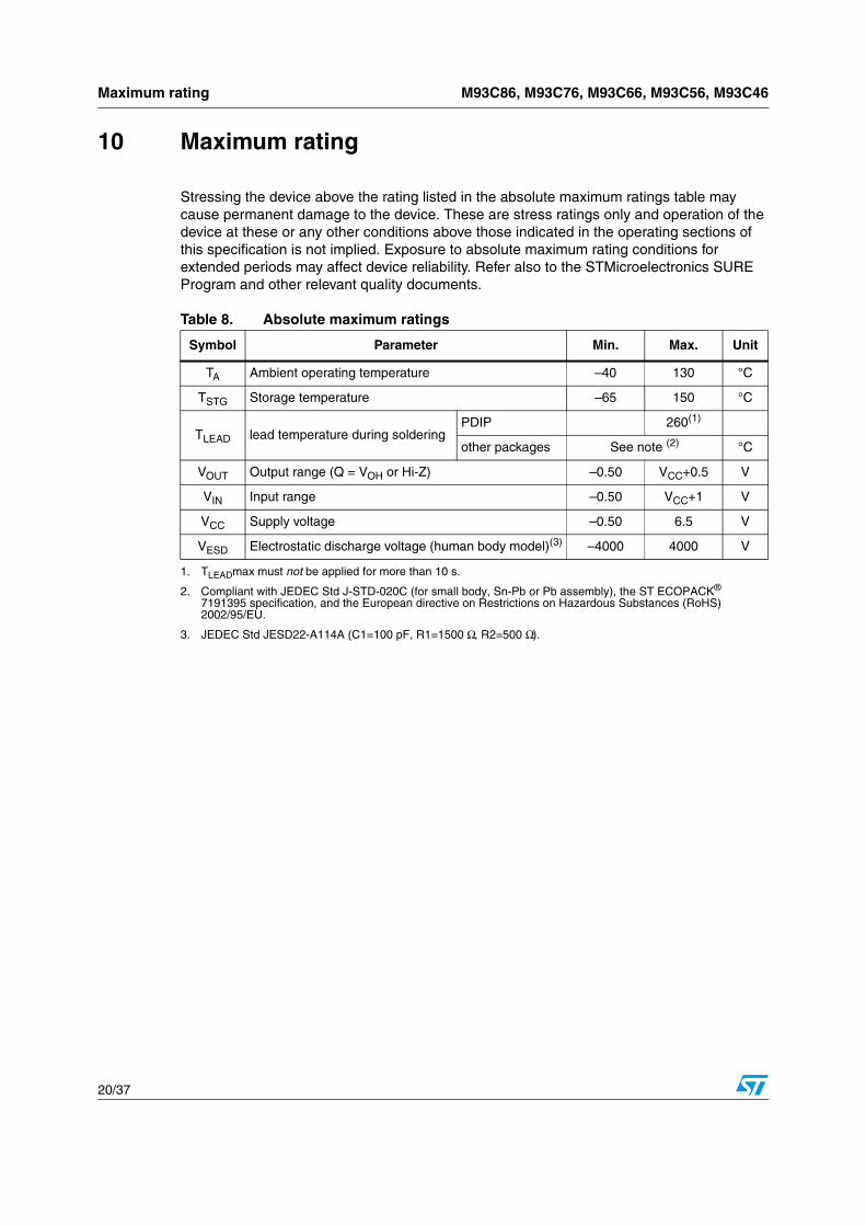
Stressing the device above the rating listed in the absolute maximum ratings table may cause permanent damage to the device. These are stress ratings only and operation of the device at these or any other conditions above those indicated in the operating sections of this specification is not implied. Exposure to absolute maximum rating conditions for extended periods may affect device reliability. Refer also to the STMicroelectronics SURE Program and other relevant quality documents.
Table 8. Absolute maximum ratings
Symbol Parameter Min. Max. Unit
TA Ambient operating temperature –40 130 °C
TSTG Storage temperature –65 150 °C
TLEAD lead temperature during solderingPDIP 260(1)
1. TLEADmax must not be applied for more than 10 s.
other packages See note (2)
2. Compliant with JEDEC Std J-STD-020C (for small body, Sn-Pb or Pb assembly), the ST ECOPACK® 7191395 specification, and the European directive on Restrictions on Hazardous Substances (RoHS) 2002/95/EU.
°C
VOUT Output range (Q = VOH or Hi-Z) –0.50 VCC+0.5 V
VIN Input range –0.50 VCC+1 V
VCC Supply voltage –0.50 6.5 V
VESD Electrostatic discharge voltage (human body model)(3)
M93C86, M93C76, M93C66, M93C56, M93C46 DC and AC parameters
21/37
11 DC and AC parameters
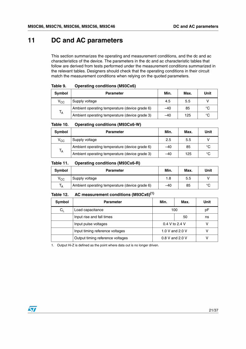
This section summarizes the operating and measurement conditions, and the dc and ac characteristics of the device. The parameters in the dc and ac characteristic tables that follow are derived from tests performed under the measurement conditions summarized in the relevant tables. Designers should check that the operating conditions in their circuit match the measurement conditions when relying on the quoted parameters.
Table 9. Operating conditions (M93Cx6)
Symbol Parameter Min. Max. Unit
VCC Supply voltage 4.5 5.5 V
TA
Ambient operating temperature (device grade 6) –40 85 °C
Ambient operating temperature (device grade 3) –40 125 °C
Table 10. Operating conditions (M93Cx6-W)
Symbol Parameter Min. Max. Unit
VCC Supply voltage 2.5 5.5 V
TA
Ambient operating temperature (device grade 6) –40 85 °C
Ambient operating temperature (device grade 3) –40 125 °C
Table 11. Operating conditions (M93Cx6-R)
Symbol Parameter Min. Max. Unit
VCC Supply voltage 1.8 5.5 V
TA Ambient operating temperature (device grade 6) –40 85 °C
Table 12. AC measurement conditions (M93Cx6)(1)
1. Output Hi-Z is defined as the point where data out is no longer driven.
Symbol Parameter Min. Max. Unit
CL Load capacitance 100 pF
Input rise and fall times 50 ns
Input pulse voltages 0.4 V to 2.4 V V
Input timing reference voltages 1.0 V and 2.0 V V
Output timing reference voltages 0.8 V and 2.0 V V
DC and AC parameters M93C86, M93C76, M93C66, M93C56, M93C46
22/37
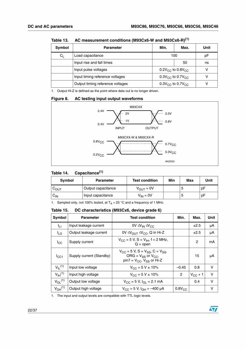
Figure 8. AC testing input output waveforms
Table 13. AC measurement conditions (M93Cx6-W and M93Cx6-R)(1)
1. Output Hi-Z is defined as the point where data out is no longer driven.
Symbol Parameter Min. Max. Unit
CL Load capacitance 100 pF
Input rise and fall times 50 ns
Input pulse voltages 0.2VCC to 0.8VCC V
Input timing reference voltages 0.3VCC to 0.7VCC V
Output timing reference voltages 0.3VCC to 0.7VCC V
Table 14. Capacitance(1)
1. Sampled only, not 100% tested, at TA = 25 °C and a frequency of 1 MHz.
Symbol Parameter Test condition Min Max Unit
COUT Output capacitance VOUT = 0V 5 pF
CIN Input capacitance VIN = 0V 5 pF
Table 15. DC characteristics (M93Cx6, device grade 6)
Symbol Parameter Test condition Min. Max. Unit
ILI Input leakage current 0V ≤ VIN ≤ VCC ±2.5 µA
ILO Output leakage current 0V ≤ VOUT ≤ VCC, Q in Hi-Z ±2.5 µA
ICC Supply current VCC = 5 V, S = VIH, f = 2 MHz,
Q = open 2 mA
ICC1 Supply current (Standby) VCC = 5 V, S = VSS, C = VSS,
ORG = VSS or VCC,pin7 = VCC, VSS or Hi-Z
15 µA
VIL(1)
1. The input and output levels are compatible with TTL logic levels.
Input low voltage VCC = 5 V ± 10% –0.45 0.8 V
VIH(1) Input high voltage VCC = 5 V ± 10% 2 VCC + 1 V
VOL(1) Output low voltage VCC = 5 V, IOL = 2.1 mA 0.4 V
VOH(1) Output high voltage VCC = 5 V, IOH = –400 µA 0.8VCC V
AI02553
2.4V
0.4V
2.0V
0.8V
2V
1V
INPUT OUTPUT
0.8VCC
0.2VCC
0.7VCC
0.3VCC
M93CXX-W & M93CXX-R
M93CXX
M93C86, M93C76, M93C66, M93C56, M93C46 DC and AC parameters
23/37
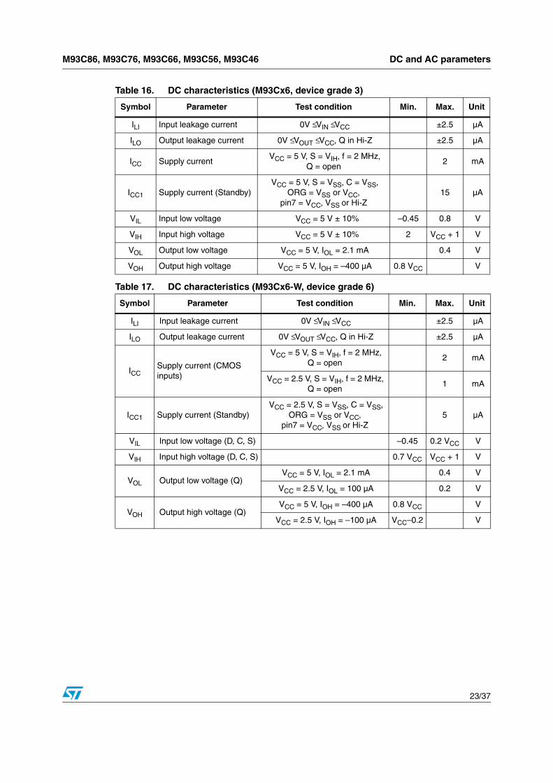
Table 16. DC characteristics (M93Cx6, device grade 3)
Symbol Parameter Test condition Min. Max. Unit
ILI Input leakage current 0V ≤ VIN ≤ VCC ±2.5 µA
ILO Output leakage current 0V ≤ VOUT ≤ VCC, Q in Hi-Z ±2.5 µA
ICC Supply current VCC = 5 V, S = VIH, f = 2 MHz,
Q = open 2 mA
ICC1 Supply current (Standby) VCC = 5 V, S = VSS, C = VSS,
ORG = VSS or VCC,pin7 = VCC, VSS or Hi-Z
15 µA
VIL Input low voltage VCC = 5 V ± 10% –0.45 0.8 V
VIH Input high voltage VCC = 5 V ± 10% 2 VCC + 1 V
VOL Output low voltage VCC = 5 V, IOL = 2.1 mA 0.4 V
VOH Output high voltage VCC = 5 V, IOH = –400 µA 0.8 VCC V
Table 17. DC characteristics (M93Cx6-W, device grade 6)
Symbol Parameter Test condition Min. Max. Unit
ILI Input leakage current 0V ≤ VIN ≤ VCC ±2.5 µA
ILO Output leakage current 0V ≤ VOUT ≤ VCC, Q in Hi-Z ±2.5 µA
ICCSupply current (CMOS inputs)
VCC = 5 V, S = VIH, f = 2 MHz,Q = open
2 mA
VCC = 2.5 V, S = VIH, f = 2 MHz, Q = open
1 mA
ICC1 Supply current (Standby) VCC = 2.5 V, S = VSS, C = VSS,
ORG = VSS or VCC,pin7 = VCC, VSS or Hi-Z
5 µA
VIL Input low voltage (D, C, S) –0.45 0.2 VCC V
VIH Input high voltage (D, C, S) 0.7 VCC VCC + 1 V
VOL Output low voltage (Q) VCC = 5 V, IOL = 2.1 mA 0.4 V
VCC = 2.5 V, IOL = 100 µA 0.2 V
VOH Output high voltage (Q) VCC = 5 V, IOH = –400 µA 0.8 VCC V
VCC = 2.5 V, IOH = –100 µA VCC–0.2 V
DC and AC parameters M93C86, M93C76, M93C66, M93C56, M93C46
24/37
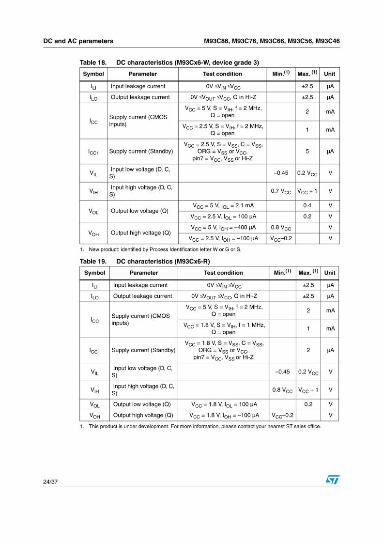
Table 18. DC characteristics (M93Cx6-W, device grade 3)
Symbol Parameter Test condition Min.(1)
1. New product: identified by Process Identification letter W or G or S.
Max. (1) Unit
ILI Input leakage current 0V ≤ VIN ≤ VCC ±2.5 µA
ILO Output leakage current 0V ≤ VOUT ≤ VCC, Q in Hi-Z ±2.5 µA
ICCSupply current (CMOS inputs)
VCC = 5 V, S = VIH, f = 2 MHz,Q = open
2 mA
VCC = 2.5 V, S = VIH, f = 2 MHz, Q = open
1 mA
ICC1 Supply current (Standby) VCC = 2.5 V, S = VSS, C = VSS,
ORG = VSS or VCC,pin7 = VCC, VSS or Hi-Z
5 µA
VIL Input low voltage (D, C, S)
–0.45 0.2 VCC V
VIH Input high voltage (D, C, S)
0.7 VCC VCC + 1 V
VOL Output low voltage (Q) VCC = 5 V, IOL = 2.1 mA 0.4 V
VCC = 2.5 V, IOL = 100 µA 0.2 V
VOH Output high voltage (Q) VCC = 5 V, IOH = –400 µA 0.8 VCC V
VCC = 2.5 V, IOH = –100 µA VCC–0.2 V
Table 19. DC characteristics (M93Cx6-R)
Symbol Parameter Test condition Min.(1)
1. This product is under development. For more information, please contact your nearest ST sales office.
Max. (1) Unit
ILI Input leakage current 0V ≤ VIN ≤ VCC ±2.5 µA
ILO Output leakage current 0V ≤ VOUT ≤ VCC, Q in Hi-Z ±2.5 µA
ICCSupply current (CMOS inputs)
VCC = 5 V, S = VIH, f = 2 MHz,Q = open
2 mA
VCC = 1.8 V, S = VIH, f = 1 MHz, Q = open
1 mA
ICC1 Supply current (Standby) VCC = 1.8 V, S = VSS, C = VSS,
ORG = VSS or VCC,pin7 = VCC, VSS or Hi-Z
2 µA
VIL Input low voltage (D, C, S)
–0.45 0.2 VCC V
VIH Input high voltage (D, C, S)
0.8 VCC VCC + 1 V
VOL Output low voltage (Q) VCC = 1.8 V, IOL = 100 µA 0.2 V
VOH Output high voltage (Q) VCC = 1.8 V, IOH = –100 µA VCC–0.2 V
M93C86, M93C76, M93C66, M93C56, M93C46 DC and AC parameters
25/37
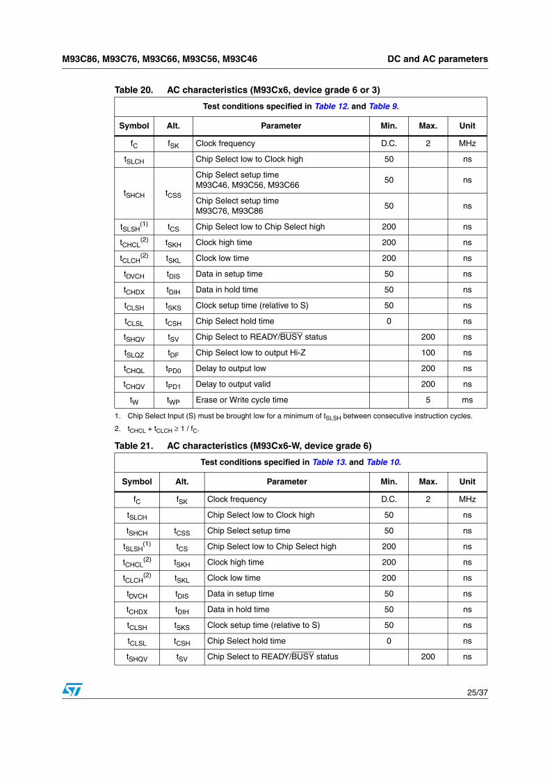
Table 20. AC characteristics (M93Cx6, device grade 6 or 3)
Test conditions specified in Table 12. and Table 9.
Symbol Alt. Parameter Min. Max. Unit
fC fSK Clock frequency D.C. 2 MHz
tSLCH Chip Select low to Clock high 50 ns
tSHCH tCSS
Chip Select setup timeM93C46, M93C56, M93C66
50 ns
Chip Select setup timeM93C76, M93C86
50 ns
tSLSH(1)
1. Chip Select Input (S) must be brought low for a minimum of tSLSH between consecutive instruction cycles.
tCS Chip Select low to Chip Select high 200 ns
tCHCL(2)
2. tCHCL + tCLCH ≥ 1 / fC.
tSKH Clock high time 200 ns
tCLCH(2) tSKL Clock low time 200 ns
tDVCH tDIS Data in setup time 50 ns
tCHDX tDIH Data in hold time 50 ns
tCLSH tSKS Clock setup time (relative to S) 50 ns
tCLSL tCSH Chip Select hold time 0 ns
tSHQV tSV Chip Select to READY/BUSY status 200 ns
tSLQZ tDF Chip Select low to output Hi-Z 100 ns
tCHQL tPD0 Delay to output low 200 ns
tCHQV tPD1 Delay to output valid 200 ns
tW tWP Erase or Write cycle time 5 ms
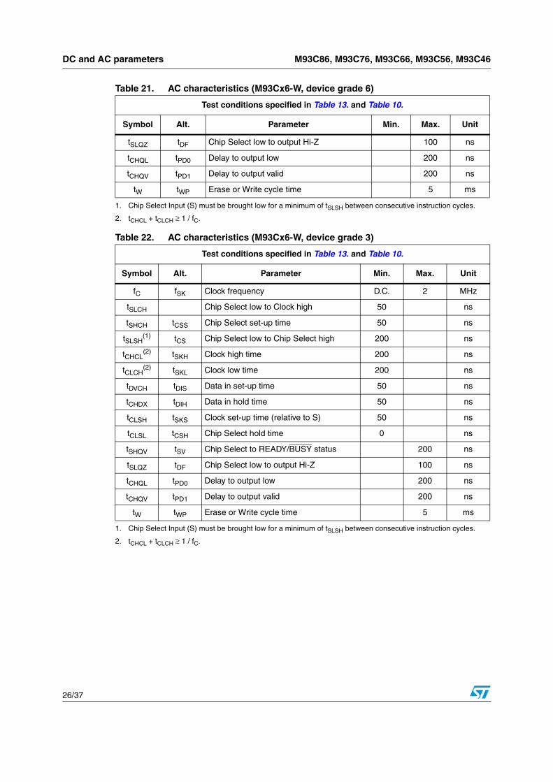
Table 21. AC characteristics (M93Cx6-W, device grade 6)
Test conditions specified in Table 13. and Table 10.
Symbol Alt. Parameter Min. Max. Unit
fC fSK Clock frequency D.C. 2 MHz
tSLCH Chip Select low to Clock high 50 ns
tSHCH tCSS Chip Select setup time 50 ns
tSLSH(1) tCS Chip Select low to Chip Select high 200 ns
tCHCL(2) tSKH Clock high time 200 ns
tCLCH(2) tSKL Clock low time 200 ns
tDVCH tDIS Data in setup time 50 ns
tCHDX tDIH Data in hold time 50 ns
tCLSH tSKS Clock setup time (relative to S) 50 ns
tCLSL tCSH Chip Select hold time 0 ns
tSHQV tSV Chip Select to READY/BUSY status 200 ns
DC and AC parameters M93C86, M93C76, M93C66, M93C56, M93C46
26/37
tSLQZ tDF Chip Select low to output Hi-Z 100 ns
tCHQL tPD0 Delay to output low 200 ns
tCHQV tPD1 Delay to output valid 200 ns
tW tWP Erase or Write cycle time 5 ms
1. Chip Select Input (S) must be brought low for a minimum of tSLSH between consecutive instruction cycles.
2. tCHCL + tCLCH ≥ 1 / fC.
Table 22. AC characteristics (M93Cx6-W, device grade 3)
Test conditions specified in Table 13. and Table 10.
Symbol Alt. Parameter Min. Max. Unit
fC fSK Clock frequency D.C. 2 MHz
tSLCH Chip Select low to Clock high 50 ns
tSHCH tCSS Chip Select set-up time 50 ns
tSLSH(1)
1. Chip Select Input (S) must be brought low for a minimum of tSLSH between consecutive instruction cycles.
tCS Chip Select low to Chip Select high 200 ns
tCHCL(2)
2. tCHCL + tCLCH ≥ 1 / fC.
tSKH Clock high time 200 ns
tCLCH(2) tSKL Clock low time 200 ns
tDVCH tDIS Data in set-up time 50 ns
tCHDX tDIH Data in hold time 50 ns
tCLSH tSKS Clock set-up time (relative to S) 50 ns
tCLSL tCSH Chip Select hold time 0 ns
tSHQV tSV Chip Select to READY/BUSY status 200 ns
tSLQZ tDF Chip Select low to output Hi-Z 100 ns
tCHQL tPD0 Delay to output low 200 ns
tCHQV tPD1 Delay to output valid 200 ns
tW tWP Erase or Write cycle time 5 ms
Table 21. AC characteristics (M93Cx6-W, device grade 6)
Test conditions specified in Table 13. and Table 10.
Symbol Alt. Parameter Min. Max. Unit
M93C86, M93C76, M93C66, M93C56, M93C46 DC and AC parameters
27/37
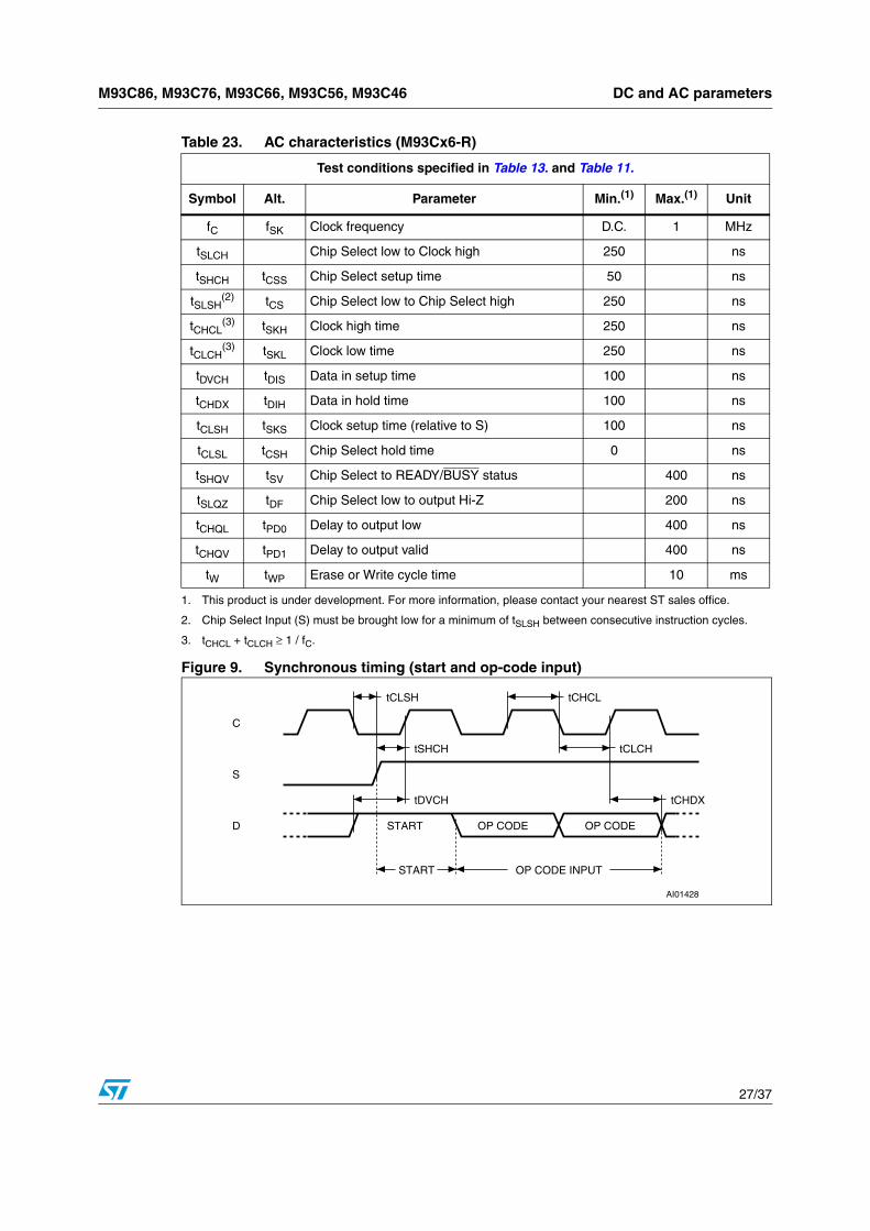
Figure 9. Synchronous timing (start and op-code input)
Table 23. AC characteristics (M93Cx6-R)
Test conditions specified in Table 13. and Table 11.
Symbol Alt. Parameter Min.(1)
1. This product is under development. For more information, please contact your nearest ST sales office.
Max.(1) Unit
fC fSK Clock frequency D.C. 1 MHz
tSLCH Chip Select low to Clock high 250 ns
tSHCH tCSS Chip Select setup time 50 ns
tSLSH(2)
2. Chip Select Input (S) must be brought low for a minimum of tSLSH between consecutive instruction cycles.
tCS Chip Select low to Chip Select high 250 ns
tCHCL(3)
3. tCHCL + tCLCH ≥ 1 / fC.
tSKH Clock high time 250 ns
tCLCH(3) tSKL Clock low time 250 ns
tDVCH tDIS Data in setup time 100 ns
tCHDX tDIH Data in hold time 100 ns
tCLSH tSKS Clock setup time (relative to S) 100 ns
tCLSL tCSH Chip Select hold time 0 ns
tSHQV tSV Chip Select to READY/BUSY status 400 ns
tSLQZ tDF Chip Select low to output Hi-Z 200 ns
tCHQL tPD0 Delay to output low 400 ns
tCHQV tPD1 Delay to output valid 400 ns
tW tWP Erase or Write cycle time 10 ms
AI01428
C
OP CODE OP CODESTART
S
D
OP CODE INPUTSTART
tDVCH
tSHCH
tCLSH tCHCL
tCLCH
tCHDX
DC and AC parameters M93C86, M93C76, M93C66, M93C56, M93C46
28/37
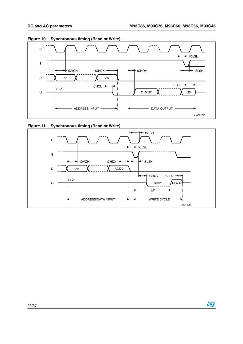
Figure 10. Synchronous timing (Read or Write)
Figure 11. Synchronous timing (Read or Write)
AI00820C
C
D
Q
ADDRESS INPUT
Hi-Z
tDVCH
tCLSL
A0
S
DATA OUTPUT
tCHQVtCHDX
tCHQL
An
tSLSH
tSLQZ
Q15/Q7 Q0
AI01429
C
D
Q
ADDRESS/DATA INPUT
Hi-Z
tDVCH
tSLCH
A0/D0
S
WRITE CYCLE
tSLSHtCHDX
An
tCLSL
tSLQZ
BUSY
tSHQV
tW
READY
M93C86, M93C76, M93C66, M93C56, M93C46 Package mechanical data
29/37
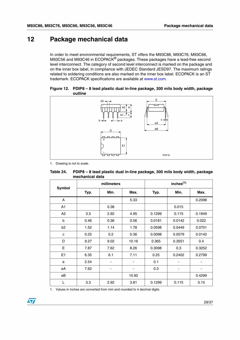
12 Package mechanical data
In order to meet environmental requirements, ST offers the M93C86, M93C76, M93C66, M93C56 and M93C46 in ECOPACK® packages. These packages have a lead-free second level interconnect. The category of second level interconnect is marked on the package and on the inner box label, in compliance with JEDEC Standard JESD97. The maximum ratings related to soldering conditions are also marked on the inner box label. ECOPACK is an ST trademark. ECOPACK specifications are available at www.st.com.
Figure 12. PDIP8 – 8 lead plastic dual in-line package, 300 mils body width, packageoutline
1. Drawing is not to scale.
Table 24. PDIP8 – 8 lead plastic dual in-line package, 300 mils body width, packagemechanical data
Symbolmillimeters inches(1)
1. Values in inches are converted from mm and rounded to 4 decimal digits.
Typ. Min. Max. Typ. Min. Max.
A 5.33 0.2098
A1 0.38 0.015
A2 3.3 2.92 4.95 0.1299 0.115 0.1949
b 0.46 0.36 0.56 0.0181 0.0142 0.022
b2 1.52 1.14 1.78 0.0598 0.0449 0.0701
c 0.25 0.2 0.36 0.0098 0.0079 0.0142
D 9.27 9.02 10.16 0.365 0.3551 0.4
E 7.87 7.62 8.26 0.3098 0.3 0.3252
E1 6.35 6.1 7.11 0.25 0.2402 0.2799
e 2.54 - - 0.1 - -
eA 7.62 - - 0.3 - -
eB 10.92 0.4299
L 3.3 2.92 3.81 0.1299 0.115 0.15
PDIP-B
A2
A1
A
L
b e
D
E1
8
1
ceA
b2
eB
E
Package mechanical data M93C86, M93C76, M93C66, M93C56, M93C46
30/37
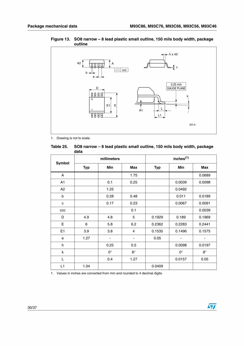
Figure 13. SO8 narrow – 8 lead plastic small outline, 150 mils body width, package outline
1. Drawing is not to scale.
Table 25. SO8 narrow – 8 lead plastic small outline, 150 mils body width, package data
Symbolmillimeters inches(1)
1. Values in inches are converted from mm and rounded to 4 decimal digits.
Typ Min Max Typ Min Max
A 1.75 0.0689
A1 0.1 0.25 0.0039 0.0098
A2 1.25 0.0492
b 0.28 0.48 0.011 0.0189
c 0.17 0.23 0.0067 0.0091
ccc 0.1 0.0039
D 4.9 4.8 5 0.1929 0.189 0.1969
E 6 5.8 6.2 0.2362 0.2283 0.2441
E1 3.9 3.8 4 0.1535 0.1496 0.1575
e 1.27 - - 0.05 - -
h 0.25 0.5 0.0098 0.0197
k 0° 8° 0° 8°
L 0.4 1.27 0.0157 0.05
L1 1.04 0.0409
SO-A
E1
8
cccb
e
A
D
c
1
E
h x 45˚
A2
k
0.25 mm
L
L1
A1
GAUGE PLANE
M93C86, M93C76, M93C66, M93C56, M93C46 Package mechanical data
31/37
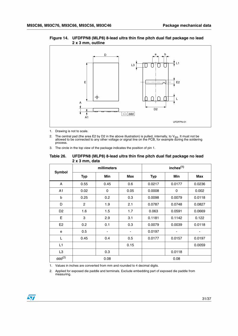
Figure 14. UFDFPN8 (MLP8) 8-lead ultra thin fine pitch dual flat package no lead 2 x 3 mm, outline
1. Drawing is not to scale.
2. The central pad (the area E2 by D2 in the above illustration) is pulled, internally, to VSS. It must not be allowed to be connected to any other voltage or signal line on the PCB, for example during the soldering process.
3. The circle in the top view of the package indicates the position of pin 1.
Table 26. UFDFPN8 (MLP8) 8-lead ultra thin fine pitch dual flat package no lead 2 x 3 mm, data
Symbolmillimeters inches(1)
1. Values in inches are converted from mm and rounded to 4 decimal digits.
Typ Min Max Typ Min Max
A 0.55 0.45 0.6 0.0217 0.0177 0.0236
A1 0.02 0 0.05 0.0008 0 0.002
b 0.25 0.2 0.3 0.0098 0.0079 0.0118
D 2 1.9 2.1 0.0787 0.0748 0.0827
D2 1.6 1.5 1.7 0.063 0.0591 0.0669
E 3 2.9 3.1 0.1181 0.1142 0.122
E2 0.2 0.1 0.3 0.0079 0.0039 0.0118
e 0.5 - - 0.0197 - -
L 0.45 0.4 0.5 0.0177 0.0157 0.0197
L1 0.15 0.0059
L3 0.3 0.0118
ddd(2)
2. Applied for exposed die paddle and terminals. Exclude embedding part of exposed die paddle from measuring.
0.08 0.08
D
E
UFDFPN-01
A
A1ddd
L1
e b
D2
L
E2
L3
Package mechanical data M93C86, M93C76, M93C66, M93C56, M93C46
32/37
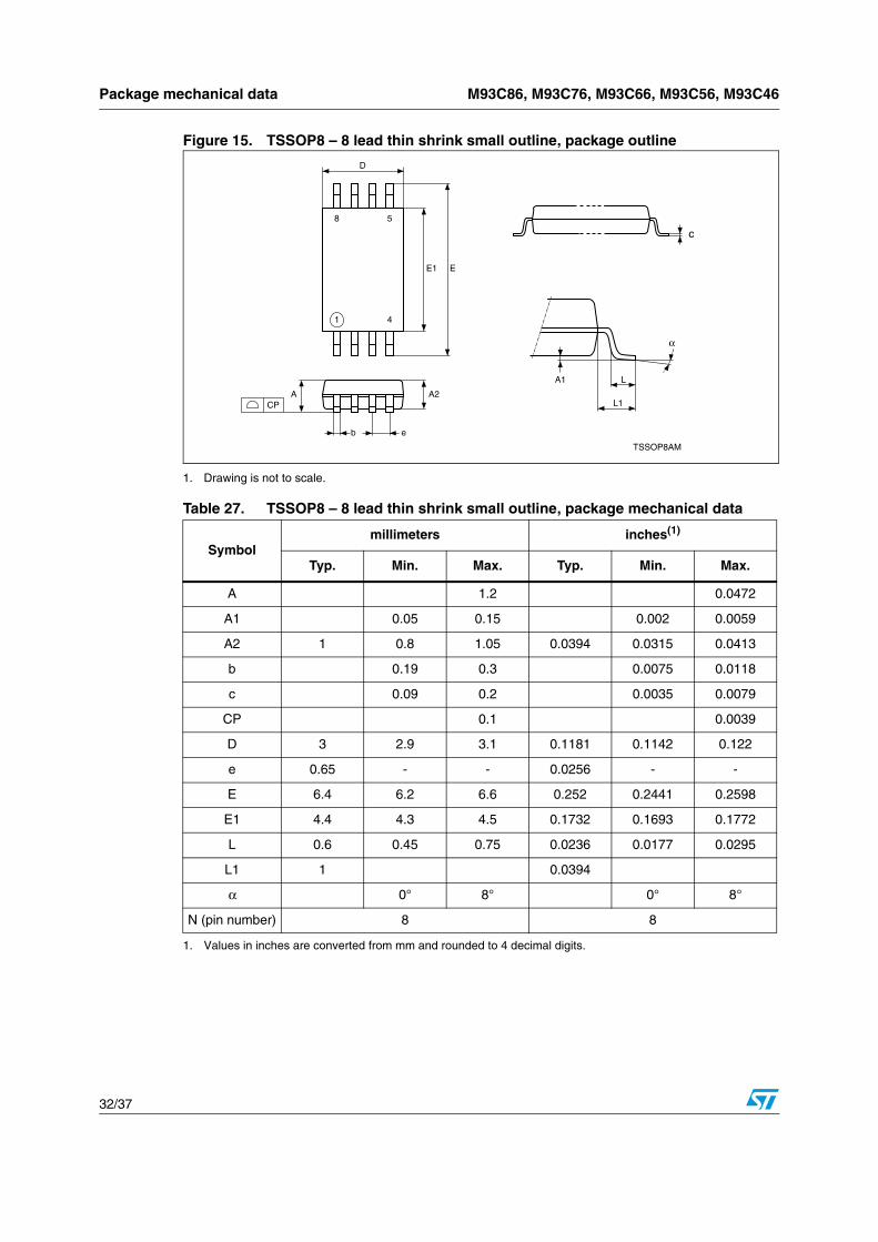
Figure 15. TSSOP8 – 8 lead thin shrink small outline, package outline
1. Drawing is not to scale.
Table 27. TSSOP8 – 8 lead thin shrink small outline, package mechanical data
Symbolmillimeters inches(1)
1. Values in inches are converted from mm and rounded to 4 decimal digits.
Typ. Min. Max. Typ. Min. Max.
A 1.2 0.0472
A1 0.05 0.15 0.002 0.0059
A2 1 0.8 1.05 0.0394 0.0315 0.0413
b 0.19 0.3 0.0075 0.0118
c 0.09 0.2 0.0035 0.0079
CP 0.1 0.0039
D 3 2.9 3.1 0.1181 0.1142 0.122
e 0.65 - - 0.0256 - -
E 6.4 6.2 6.6 0.252 0.2441 0.2598
E1 4.4 4.3 4.5 0.1732 0.1693 0.1772
L 0.6 0.45 0.75 0.0236 0.0177 0.0295
L1 1 0.0394
α 0° 8° 0° 8°
N (pin number) 8 8
TSSOP8AM
1
8
CP
c
L
EE1
D
A2A
α
eb
4
5
A1
L1
M93C86, M93C76, M93C66, M93C56, M93C46 Part numbering
33/37
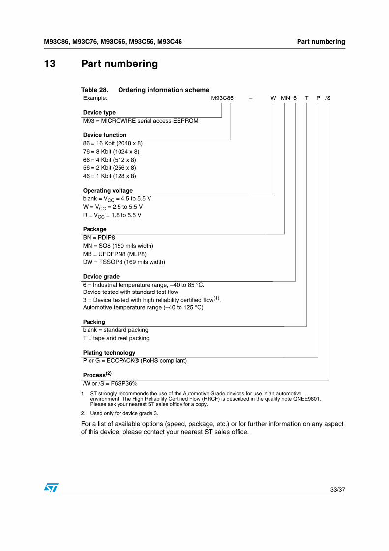
13 Part numbering
For a list of available options (speed, package, etc.) or for further information on any aspect of this device, please contact your nearest ST sales office.
Table 28. Ordering information schemeExample: M93C86 – W MN 6 T P /S
Device typeM93 = MICROWIRE serial access EEPROM
Device function86 = 16 Kbit (2048 x 8)76 = 8 Kbit (1024 x 8)66 = 4 Kbit (512 x 8)56 = 2 Kbit (256 x 8)46 = 1 Kbit (128 x 8)
Operating voltageblank = VCC = 4.5 to 5.5 VW = VCC = 2.5 to 5.5 VR = VCC = 1.8 to 5.5 V
Device grade6 = Industrial temperature range, –40 to 85 °C.Device tested with standard test flow3 = Device tested with high reliability certified flow(1).Automotive temperature range (–40 to 125 °C)
1. ST strongly recommends the use of the Automotive Grade devices for use in an automotive environment. The High Reliability Certified Flow (HRCF) is described in the quality note QNEE9801. Please ask your nearest ST sales office for a copy.
Packingblank = standard packingT = tape and reel packing
Plating technologyP or G = ECOPACK® (RoHS compliant)
Process(2)
2. Used only for device grade 3.
/W or /S = F6SP36%
Part numbering M93C86, M93C76, M93C66, M93C56, M93C46
34/37
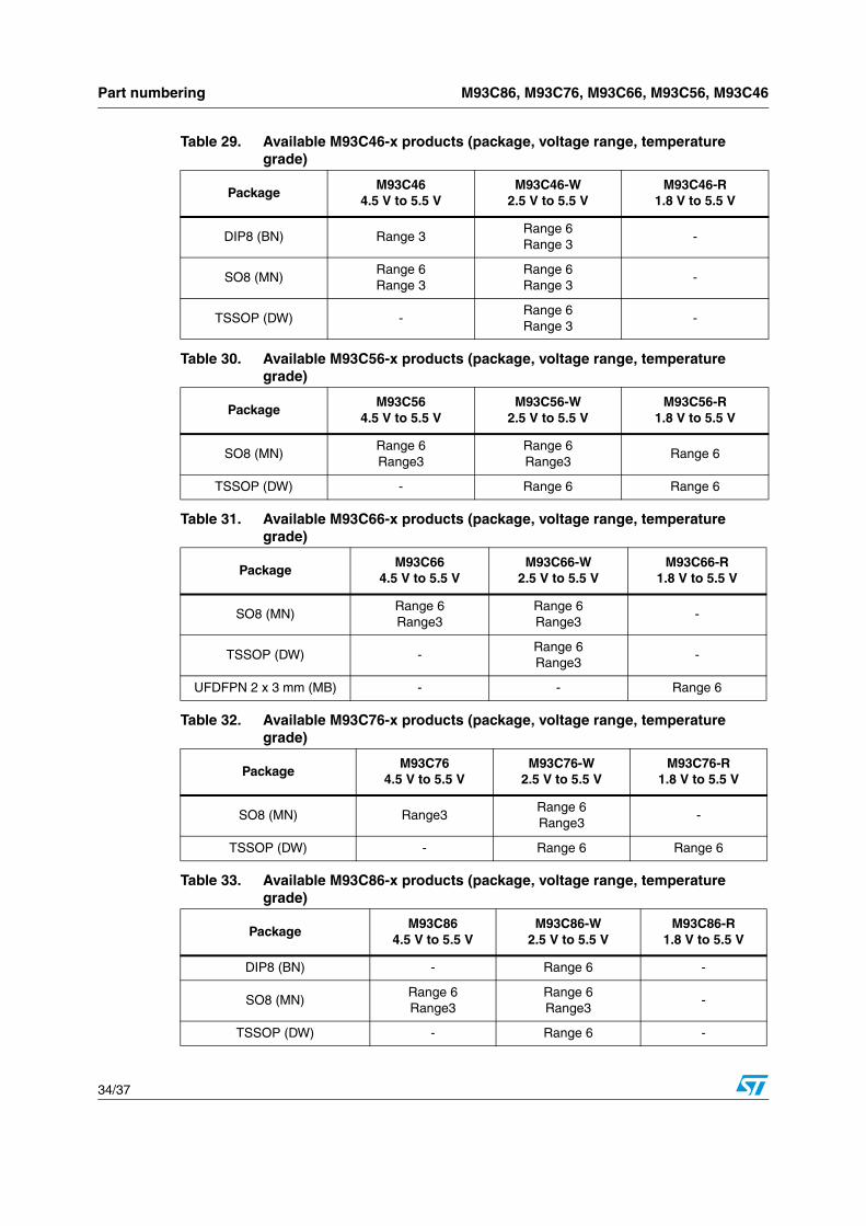
Table 29. Available M93C46-x products (package, voltage range, temperature grade)
PackageM93C46
4.5 V to 5.5 VM93C46-W
2.5 V to 5.5 VM93C46-R
1.8 V to 5.5 V
DIP8 (BN) Range 3Range 6Range 3
-
SO8 (MN)Range 6Range 3
Range 6Range 3
-
TSSOP (DW) -Range 6Range 3
-
Table 30. Available M93C56-x products (package, voltage range, temperature grade)
PackageM93C56
4.5 V to 5.5 VM93C56-W
2.5 V to 5.5 VM93C56-R
1.8 V to 5.5 V
SO8 (MN)Range 6Range3
Range 6Range3
Range 6
TSSOP (DW) - Range 6 Range 6
Table 31. Available M93C66-x products (package, voltage range, temperature grade)
PackageM93C66
4.5 V to 5.5 VM93C66-W
2.5 V to 5.5 VM93C66-R
1.8 V to 5.5 V
SO8 (MN)Range 6Range3
Range 6Range3
-
TSSOP (DW) -Range 6Range3
-
UFDFPN 2 x 3 mm (MB) - - Range 6
Table 32. Available M93C76-x products (package, voltage range, temperature grade)
PackageM93C76
4.5 V to 5.5 VM93C76-W
2.5 V to 5.5 VM93C76-R
1.8 V to 5.5 V
SO8 (MN) Range3Range 6Range3
-
TSSOP (DW) - Range 6 Range 6
Table 33. Available M93C86-x products (package, voltage range, temperature grade)
PackageM93C86
4.5 V to 5.5 VM93C86-W
2.5 V to 5.5 VM93C86-R
1.8 V to 5.5 V
DIP8 (BN) - Range 6 -
SO8 (MN)Range 6Range3
Range 6Range3
-
TSSOP (DW) - Range 6 -
M93C86, M93C76, M93C66, M93C56, M93C46 Revision history
35/37
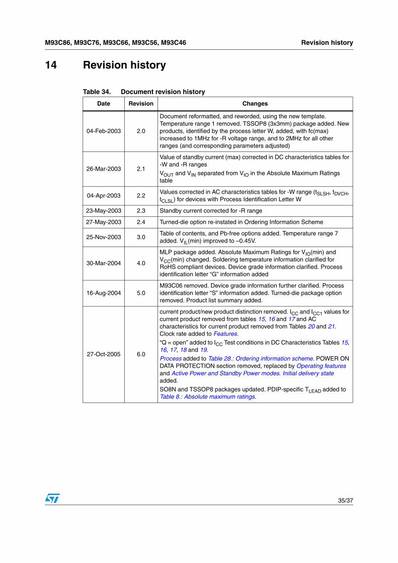
14 Revision history
Table 34. Document revision history
Date Revision Changes
04-Feb-2003 2.0
Document reformatted, and reworded, using the new template. Temperature range 1 removed. TSSOP8 (3x3mm) package added. New products, identified by the process letter W, added, with fc(max) increased to 1MHz for -R voltage range, and to 2MHz for all other ranges (and corresponding parameters adjusted)
26-Mar-2003 2.1
Value of standby current (max) corrected in DC characteristics tables for -W and -R ranges
VOUT and VIN separated from VIO in the Absolute Maximum Ratings table
04-Apr-2003 2.2Values corrected in AC characteristics tables for -W range (tSLSH, tDVCH, tCLSL) for devices with Process Identification Letter W
23-May-2003 2.3 Standby current corrected for -R range
27-May-2003 2.4 Turned-die option re-instated in Ordering Information Scheme
25-Nov-2003 3.0Table of contents, and Pb-free options added. Temperature range 7 added. VIL(min) improved to –0.45V.
30-Mar-2004 4.0
MLP package added. Absolute Maximum Ratings for VIO(min) and VCC(min) changed. Soldering temperature information clarified for RoHS compliant devices. Device grade information clarified. Process identification letter “G” information added
16-Aug-2004 5.0M93C06 removed. Device grade information further clarified. Process identification letter “S” information added. Turned-die package option removed. Product list summary added.
27-Oct-2005 6.0
current product/new product distinction removed. ICC and ICC1 values for current product removed from tables 15, 16 and 17 and AC characteristics for current product removed from Tables 20 and 21. Clock rate added to Features.
“Q = open” added to ICC Test conditions in DC Characteristics Tables 15, 16, 17, 18 and 19.
Process added to Table 28.: Ordering information scheme. POWER ON DATA PROTECTION section removed, replaced by Operating features and Active Power and Standby Power modes. Initial delivery state added.
SO8N and TSSOP8 packages updated. PDIP-specific TLEAD added to Table 8.: Absolute maximum ratings.
Revision history M93C86, M93C76, M93C66, M93C56, M93C46
36/37
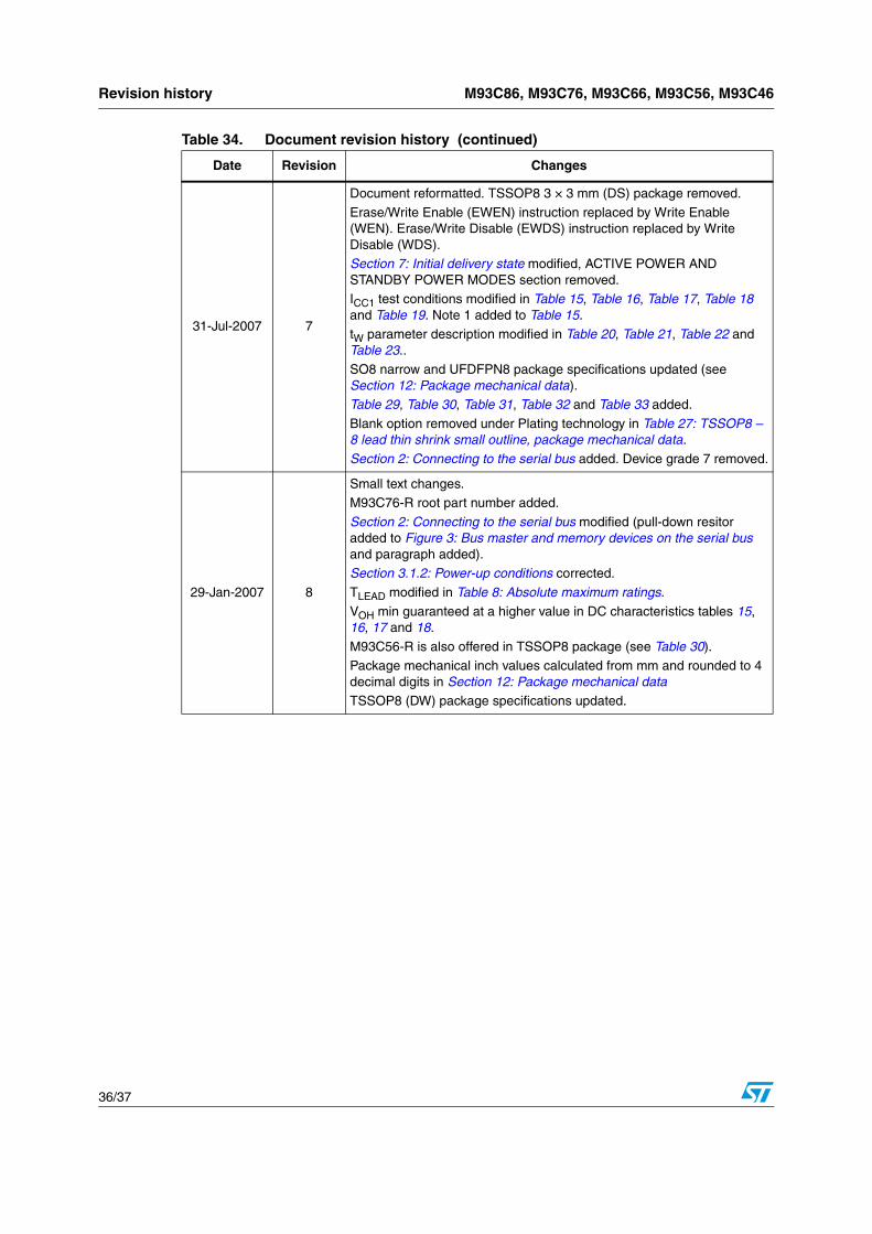
31-Jul-2007 7
Document reformatted. TSSOP8 3 × 3 mm (DS) package removed.
Erase/Write Enable (EWEN) instruction replaced by Write Enable (WEN). Erase/Write Disable (EWDS) instruction replaced by Write Disable (WDS).Section 7: Initial delivery state modified, ACTIVE POWER AND STANDBY POWER MODES section removed.ICC1 test conditions modified in Table 15, Table 16, Table 17, Table 18 and Table 19. Note 1 added to Table 15.tW parameter description modified in Table 20, Table 21, Table 22 and Table 23..SO8 narrow and UFDFPN8 package specifications updated (see Section 12: Package mechanical data).Table 29, Table 30, Table 31, Table 32 and Table 33 added.
Blank option removed under Plating technology in Table 27: TSSOP8 – 8 lead thin shrink small outline, package mechanical data.
Section 2: Connecting to the serial bus added. Device grade 7 removed.
29-Jan-2007 8
Small text changes.M93C76-R root part number added.
Section 2: Connecting to the serial bus modified (pull-down resitor added to Figure 3: Bus master and memory devices on the serial bus and paragraph added).Section 3.1.2: Power-up conditions corrected.
TLEAD modified in Table 8: Absolute maximum ratings.
VOH min guaranteed at a higher value in DC characteristics tables 15, 16, 17 and 18.
M93C56-R is also offered in TSSOP8 package (see Table 30).Package mechanical inch values calculated from mm and rounded to 4 decimal digits in Section 12: Package mechanical dataTSSOP8 (DW) package specifications updated.
Table 34. Document revision history (continued)
Date Revision Changes
M93C86, M93C76, M93C66, M93C56, M93C46
37/37
Please Read Carefully:
Information in this document is provided solely in connection with ST products. STMicroelectronics NV and its subsidiaries (“ST”) reserve theright to make changes, corrections, modifications or improvements, to this document, and the products and services described herein at anytime, without notice.
All ST products are sold pursuant to ST’s terms and conditions of sale.
Purchasers are solely responsible for the choice, selection and use of the ST products and services described herein, and ST assumes noliability whatsoever relating to the choice, selection or use of the ST products and services described herein.
No license, express or implied, by estoppel or otherwise, to any intellectual property rights is granted under this document. If any part of thisdocument refers to any third party products or services it shall not be deemed a license grant by ST for the use of such third party productsor services, or any intellectual property contained therein or considered as a warranty covering the use in any manner whatsoever of suchthird party products or services or any intellectual property contained therein.
UNLESS OTHERWISE SET FORTH IN ST’S TERMS AND CONDITIONS OF SALE ST DISCLAIMS ANY EXPRESS OR IMPLIEDWARRANTY WITH RESPECT TO THE USE AND/OR SALE OF ST PRODUCTS INCLUDING WITHOUT LIMITATION IMPLIEDWARRANTIES OF MERCHANTABILITY, FITNESS FOR A PARTICULAR PURPOSE (AND THEIR EQUIVALENTS UNDER THE LAWSOF ANY JURISDICTION), OR INFRINGEMENT OF ANY PATENT, COPYRIGHT OR OTHER INTELLECTUAL PROPERTY RIGHT.
UNLESS EXPRESSLY APPROVED IN WRITING BY AN AUTHORIZED ST REPRESENTATIVE, ST PRODUCTS ARE NOTRECOMMENDED, AUTHORIZED OR WARRANTED FOR USE IN MILITARY, AIR CRAFT, SPACE, LIFE SAVING, OR LIFE SUSTAININGAPPLICATIONS, NOR IN PRODUCTS OR SYSTEMS WHERE FAILURE OR MALFUNCTION MAY RESULT IN PERSONAL INJURY,DEATH, OR SEVERE PROPERTY OR ENVIRONMENTAL DAMAGE. ST PRODUCTS WHICH ARE NOT SPECIFIED AS "AUTOMOTIVEGRADE" MAY ONLY BE USED IN AUTOMOTIVE APPLICATIONS AT USER’S OWN RISK.
Resale of ST products with provisions different from the statements and/or technical features set forth in this document shall immediately voidany warranty granted by ST for the ST product or service described herein and shall not create or extend in any manner whatsoever, anyliability of ST.
ST and the ST logo are trademarks or registered trademarks of ST in various countries.
Information in this document supersedes and replaces all information previously supplied.
The ST logo is a registered trademark of STMicroelectronics. All other names are the property of their respective owners.
Australia - Belgium - Brazil - Canada - China - Czech Republic - Finland - France - Germany - Hong Kong - India - Israel - Italy - Japan - Malaysia - Malta - Morocco - Singapore - Spain - Sweden - Switzerland - United Kingdom - United States of America