Contents Page1. Technical Specifications, Connections, and Chassis
Overview 22. Safety Instructions, Warnings, and Notes 53. Directions for Use 64. Mechanical Instructions 75. Service Modes, Error Codes, and Fault Finding 126. Block Diagrams, Test Point Overviews, and
Waveforms 257. Circuit Diagrams and PWB Layouts 258. Alignments 269. Circuit Descriptions, Abbreviation List, and IC Data
Sheets 2910. Spare Parts List 3411. Revision List 34
Technical Specifications, Connections, and Chassis OverviewEN 2 LGE PDP 2K61.
1. Technical Specifications, Connections, and Chassis Overview
Index of this chapter:1.1 Technical Specifications PDP42X3*1.1.1 General Specification1.1.2 Definitions1.1.3 Chassis Overview
1.1 Technical Specifications PDP42X3*
The PDP Module is divided into a Panel part and a Drive part. The Panel part consists of Electrodes, Phosphor, various dielectrics, and gas, while the Drive part includes electronic circuitry and PWBs.
1.1.1 General Specification
Table 1-1 General Specifications
1.1.2 Definitions
Figure 1-1 Definition of module position
Figure 1-2 Identification label
1. Model name.2. Bar code (Code 128, contains the manufacture no.).3. Manufacture no. (Module serial no.).4. The trade name of LG Electronics.5. Manufacture date (Year & Month).6. The place of origin.7. Model suffix.
Figure 1-3 Voltage label (on rear side of module)
Model Name PDP42X3*
Number Of Pixels (H x V) 1024 (*3) x 768
Pixel Pitch (H x V µm) 900 x 676
Cell Pitch (H x V µm) 300 x 676 (base: Green Cell)
Display Area (H x V mm) 921.6 x 519.2 ± 0.5
Outline Dimension (H x V x D mm) 1005 x 597 x 61.2 ± 1Colour Arrangement RGB closed type
Number Of Colours (R x G x B) 1024 x 1024 x 1024 (1,073,741,824)
Weight 15.3 ± 0.5 kg
Aspect Ratio 16 : 9
Peak Brightness Typical 1200 cd/m2 (1 % white window)Average 140 : 1 (Light room 100 Lx at centre)
Contrast Ratio Typical 10000 : 1 (Dark room 1 % white window, white window pattern at centre)
Power Consumption Max. 330 W (Full White)
Lifetime Over 60,000 hours (initial brightness 1/2)
G_16390_001.eps290607
t s u a h x E e l o h
1 g n o l
2 g n o l
1 t r o h s
2 t r o h s
g 2-1 n o l P C T • • • • • • • • 2 2 - 2 g n o l P C T
e l u d o m f o e d i s Rear *
G_16390_002.eps020806
1
2
3
4 5 6
7
c s V y V - p u t e s V b z V
G_16391_001.eps290607
Technical Specifications, Connections, and Chassis Overview EN 3LGE PDP 2K6 1.
Figure 1-4 Part number printing (on board)
Figure 1-5 Part number label (on board)
Figure 1-6 TCP serial number (on TCP)
PCB PART NO.
G_16390_008.eps040806
G_16390_005.eps020806
BOARDSERIAL NR.
BOARDNAME
BOARD ASSYPART NR.
G_16390_007.eps030806
TCP SERIAL NO.
Technical Specifications, Connections, and Chassis OverviewEN 4 LGE PDP 2K61.
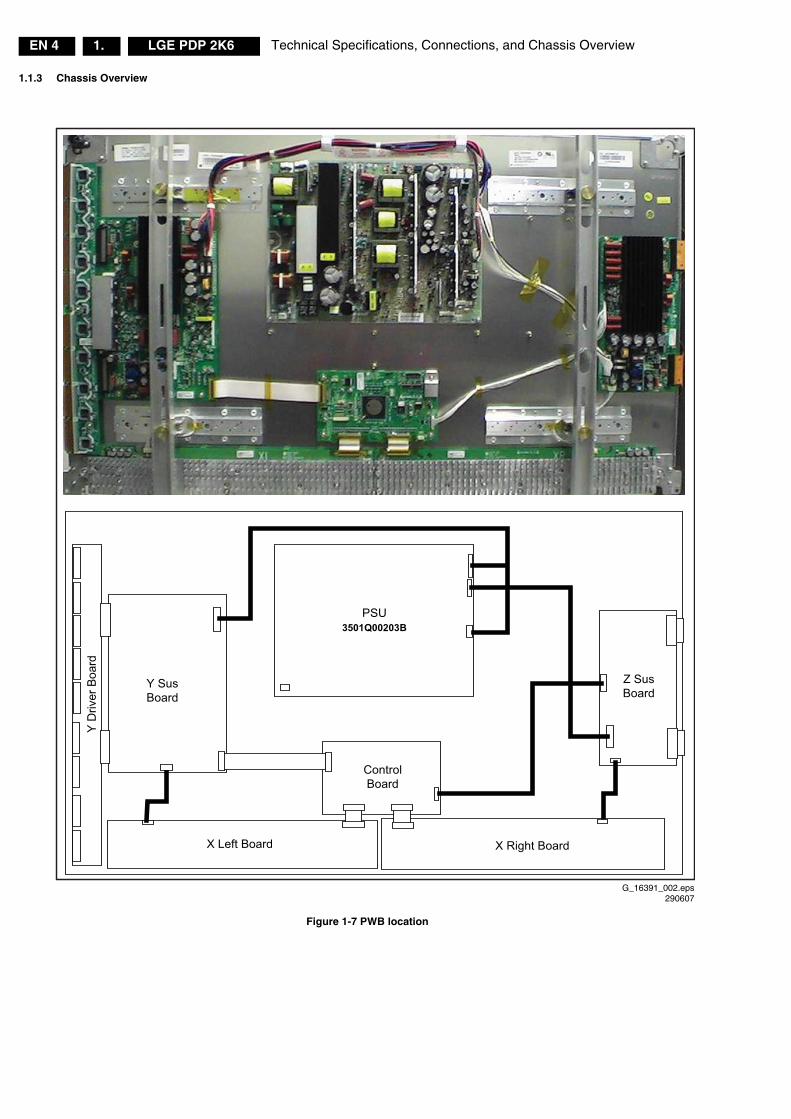
1.1.3 Chassis Overview
Figure 1-7 PWB location
G_16391_002.eps290607
Control Board
Z Sus Board
Y Sus Board
X Right BoardX Left Board
Y D
river
Boa
rd
PSU3501Q00203B
Safety Instructions, Warnings, and Notes EN 5LGE PDP 2K6 2.
2. Safety Instructions, Warnings, and Notes
Index of this chapter:2.1 Warnings
Notes:• Only authorised persons should perform servicing of this
module.• When using/handling this unit, pay special attention to the
PDP Module: it should not be enforced into any other way then next rules, warnings, and/or cautions.
• "Warning" indicates a hazard that may lead to death or injury if the warning is ignored and the product is handled incorrectly.
• "Caution" indicates a hazard that can lead to injury or damage to property if the caution is ignored and the product is handled incorrectly.
2.1 Warnings
1. Do not touch the Signal and Power Connectors while this product operates. Do not touch EMI ground part and Heat Sink of Film Filter.
2. Do not supply a voltage higher than specified to this product. This may damage the product or can create hazardous situations.
3. Do not use this product in locations where the humidity is extremely high, where it may be splashed with water, or where flammable materials surround it. Do not install or use the product in a location that does no satisfy specified environmental conditions. This may damage the product or can create hazardous situations.
4. If a foreign substance (such as water, metal, or liquid) gets inside the product, immediately turn "OFF" the power. Continuing to use the product may cause electric shock or can create hazardous situations.
5. If the product emits smoke and abnormal smell, or makes an abnormal sound, immediately turn "OFF" the power. Continuing to use the product may cause electric shock or can create hazardous situations.
6. Do not (dis)connect the connector while power to the product is "ON". It takes some time for the voltage to drop to a sufficiently low level after the power has been turned "OFF". Confirm that the voltage has dropped to a safe level before (dis)connecting the connector.
7. Do not pull out or insert the power cable from/to an outlet with wet hands. It may cause electric shock.
8. Do not damage or modify the power cable. It may cause electric shock or can create hazardous situations.
9. If the power cable is damaged, or if the connector is loose, do not use the product, otherwise, this can lead to hazardous situations or may cause electric shock.
10. If the power connector, or the connector of the power cable, is dirty or dusty, wipe it with a dry cloth. Otherwise, this can lead to hazardous situations.
11. The PDP module uses a high voltage (max. 450 VDC). Keep the cautions concerning electric shock and do not touch the device circuitry handling the PDP unit. And because the capacitors of the device circuitry may remain charged at the moment of Power "OFF", standing for 1 minute is required in order to touch the device circuitry.
12. Because the PDP module emits heat from the glass panel part and the drive circuitry, the environmental temperature must not be over 40 deg. C. The temperature of the glass panel part is especially high owing to heat from internal drive circuitry. And because the PDP module is driven by high voltage, it must avoid conductive materials.
13. If inserting components or circuit boards in order to repair, be sure to fix a lead line to the connector before soldering.
14. If inserting high-power resistors (metal-oxide film resistor or metal film resistor) in order to repair, insert it 10 mm away from a board.
15. During repairs, high voltage or high temperature components must be put away from a lead line.
16. This is a cold chassis but you better use an isolation transformer for safety during repairs. If repairing the electricity source part, you MUST use the isolation transformer.
17. Do not place an object on the glass surface of the display. The glass may break or be scratched.
18. This product may be damaged if it is subjected to excessive stresses (such as excessive voltage, current, or temperature). The absolute maximum ratings specify the limits of these stresses.
19. The recommended operating conditions are conditions in which the normal operation of this product is guaranteed. All the rated values of the electrical specifications are guaranteed within these conditions. Always use the product within the range of the recommended operating conditions. Otherwise, the reliability of the product may be degraded.
20. This product has a glass display surface. Design your system so that excessive shock and load are not applied to the glass. Exercise care that the vent at the corner of the glass panel is not damaged. If the glass panel or vent is damaged, the product is inoperable.
21. Do not cover or wrap the product with a cloth or other covering while power is supplied to the product.
22. Before turning on power to the product, check the wiring of the product and confirm that the supply voltage is within the rated voltage range. If the wiring is wrong or if a voltage outside the rated range is applied, the product may malfunction or be damaged.
23. Do not store this product in a location where temperature and humidity are high. This may cause the product to malfunction. Because this product uses a discharge phenomenon, it may take time to light (operation may be delayed) when the product is used after it has been stored for a long time. In this case, it is recommended to light all cells for about 2 hours (aging).
24. This product is made from various materials such as glass, metal, and plastic. When discarding it, be sure to contact a professional waste disposal operator.
25. If faults occur due to arbitrary modification or disassembly, LG Electronics is not responsible for function, quality or other items.
26. Use of the product with a combination of parameters, conditions, or logic not specified in the specifications of this product is not guaranteed. If intending to use the product in such a way, be sure to consult LGE in advance.
27. Within the warranty period, general faults that occur due to defects in components such as ICs will be rectified by LGE without charge. However, IMAGE STICKING due to misapplying the above provision (12), is not included in the warranty. Repairs due to the other faults may be charged for depending on responsibility for the faults.
28. While assembling the PDP module into a set, use the EMI ground part of the Film Filter for grounding, BEFORE removing the protective film, to prevent that static electricity can damage the TCPs or boards
Directions for UseEN 6 LGE PDP 2K63.
3. Directions for Use
Not applicable.
Mechanical Instructions EN 7LGE PDP 2K6 4.
4. Mechanical Instructions
Index of this chapter:4.1 Mechanical Overviews4.2 Panel/assy removal4.2.1 Power Supply Unit4.2.2 Control Board4.2.3 Y Sustain Board4.2.4 Y Driver Board4.2.5 Z-Sustain board4.2.6 X-board
4.1 Mechanical Overviews
Figure 4-1 Cable dressing
Table 4-1 Cable function
G_16391_004.eps020707
8
4
1
2 3
6
5
7
Cable No. Function
1 Drive signal for Y waveform
2 & 3 RGB data to be transferred to panel
4 & 5 5V and Va supply for X-boards Left and Right
6 Drive signal for Z-waveform
7 & 8 Va, Vs and 5 V supply for PDP operation
Mechanical InstructionsEN 8 LGE PDP 2K64.
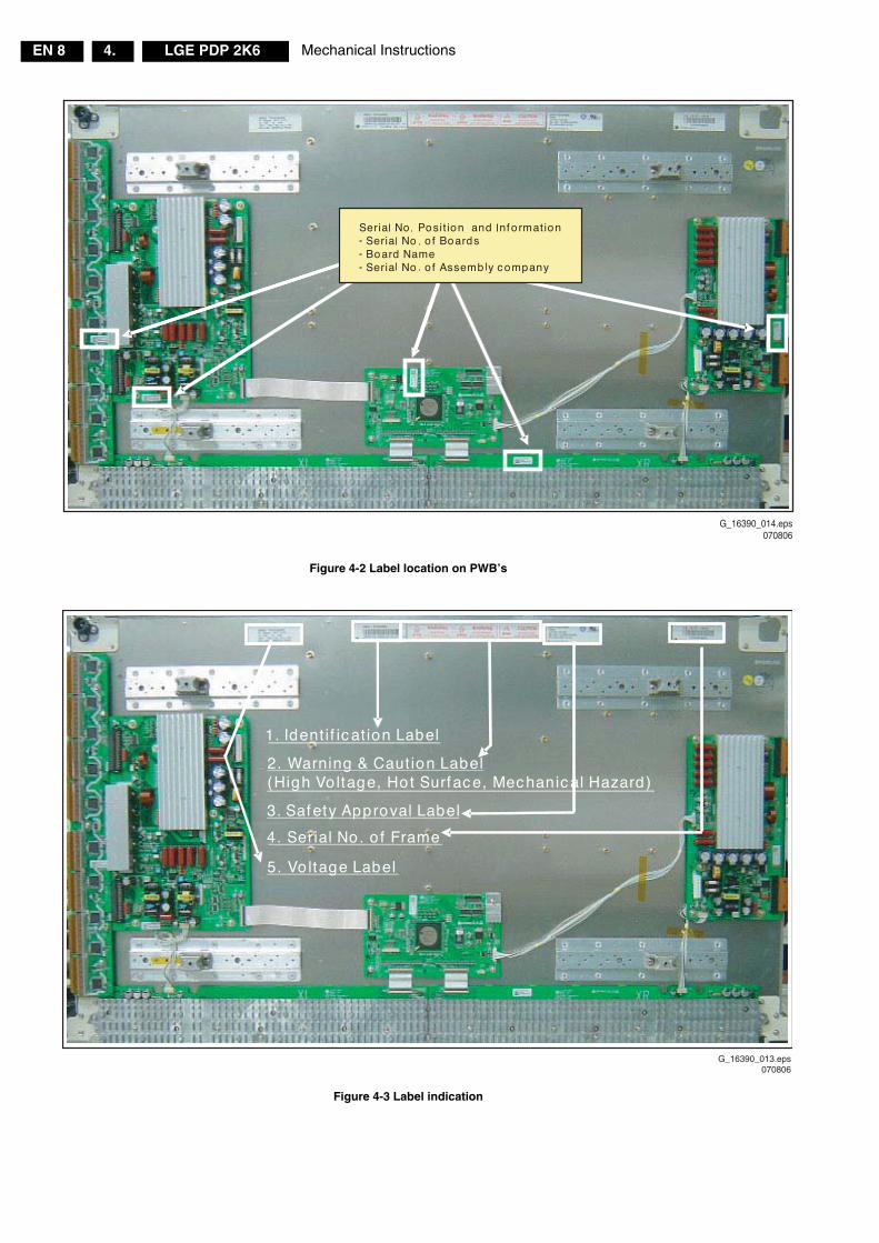
Figure 4-2 Label location on PWB’s
Figure 4-3 Label indication
G_16390_014.eps070806
G_16390_013.eps070806
Mechanical Instructions EN 9LGE PDP 2K6 4.
Figure 4-4 Label information (1)
Figure 4-5 Label information (2)
4.2 Panel/assy removal
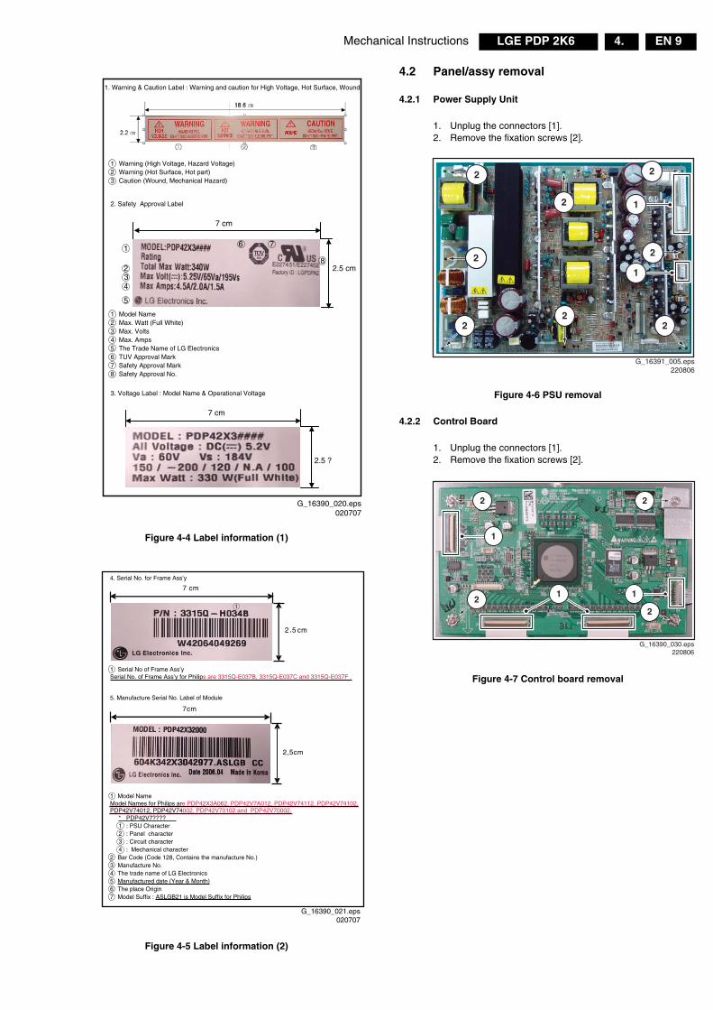
4.2.1 Power Supply Unit
1. Unplug the connectors [1].2. Remove the fixation screws [2].
Figure 4-6 PSU removal
4.2.2 Control Board
1. Unplug the connectors [1].2. Remove the fixation screws [2].
Figure 4-7 Control board removal
1. Warning & Caution Label : Warning and caution for High Voltage, Hot Surface, Wound
1 Model Name2 Max. Watt (Full White) 3 Max. Volts 4 Max. Amps 5 The Trade Name of LG Electronics6 TUV Approval Mark 7 Safety Approval Mark8 Safety Approval No.
3. Voltage Label : Model Name & Operational Voltage
2.5 ?
7 cm
G_16390_020.eps020707
4. Serial No. for Frame Ass’y
1 Serial No of Frame Ass’y Serial No. of Frame Ass’y for Philips are 3315Q-E037B, 3315Q-E037C and 3315Q-E037F .
5. Manufacture Serial No. Label of Module
1 Model NameModel Names for Philips are PDP42X3A062, PDP42V7A012, PDP42V74112, PDP42V74102,PDP42V74012, PDP42V74002, PDP42V70102 and PDP42V70002.
2 Bar Code (Code 128, Contains the manufacture No.) 3 Manufacture No. 4 The trade name of LG Electronics5 Manufactured date (Year & Month)6 The place Origin7 Model Suffix : ASLGB21 is Model Suffix for Philips
G_16390_021.eps020707
G_16391_005.eps220806
1
1
22
2
2
2
2
12
2
G_16390_030.eps220806
1
2
2
2
1
2
1
Mechanical InstructionsEN 10 LGE PDP 2K64.
4.2.3 Y Sustain Board
1. Unplug the connectors [1].2. Remove the fixation screws [2].3. Slide the board to the right, while unplugging connectors
[3]. Do not touch the heatsink!
Figure 4-8 Y-SUS board removal
4.2.4 Y Driver Board
1. Remove the Y-SUS board [1], as described previously.2. Remove the fixation screws [2].3. Separate the TCP’s [3].
Figure 4-9 Y driver board removal
Figure 4-10 TCP Separation
G_16390_031.eps010906
1
2
2
2
2
2
22
1
13
3
G_16390_032.eps010906
3
2
2
1
2
F_15590_050.eps040705
Mechanical Instructions EN 11LGE PDP 2K6 4.
4.2.5 Z-Sustain board
1. Unplug the connectors [1].2. Remove the fixation screws [2].3. Slide the board to the right, while unplugging connectors
[3]. Do not touch the heatsink!4. Pull out the locks of the FPC’s [3} as indicated by the
arrows.5. Condition in Lock part is pulled.6. Pull FPC as shown by arrow.
Figure 4-11 Z-SUS board removal
Figure 4-12 FPC removal
4.2.6 X-board
1. Unplug the power cable.2. Unplug the signal cable.3. Remove the heatsink.4. Separate the TCP’s [1].5. Remove the fixation screws [2].
Figure 4-13 X board removal 1/2
Figure 4-14 X board removal 2/2
Figure 4-15 TCP Separation
G_16390_033.eps0108069
1
12
22
2
3
3
2
F_15590_052.eps040705
Signal cables
G_16390_028.eps010906
cablesPower
X Right board
G_16390_027.eps220806
X Left board
21
12
G_16390_034.eps100806
Service Modes, Error Codes, and Fault FindingEN 12 LGE PDP 2K65.
5. Service Modes, Error Codes, and Fault Finding
Index of this chapter:5.1 Quick Module Check5.1.1 No Display5.1.2 Bar Defect (Vertical)5.1.3 Line Defect (Vertical)5.1.4 Bar Defect (Horizontal)5.1.5 Line Defect (Horizontal)
5.1.6 Mis-discharge Defect5.2 Detailed Module Check5.2.1 No Display5.2.2 Display Defects5.2.3 Checking for Component Damage5.3 Defect Description Form
5.1 Quick Module Check
Figure 5-1 Logical judgement
Figure 5-2 Quick check
What kind of defect?
Horizontal defect?
Vertical defect?
Please follow the “No display” trouble shooting way (see figure below) No display?
Bar defect appeared? Please follow “Bar defect” trouble shootingway (later on in this chapter)
Line defect
Please follow the “Line defect” trouble shooting way (later on in this chapter)
Mis–dischargeon screen? Please follow the “Mis-discharge” trouble shooting way (later on in this chapter)
G_16390_018.eps300806
Y
Y
Y
Y
N
N
N
N
Y
Y
Trouble Shooting
Horizontal defect?
Vertical defect?
Mis –dischargeon screen?
No display?
Check model No. of module, all connectors and cables.
Check power protection Check -Vy and Vsc Check Oscillator Ctrl B/D Input
Service Modes, Error Codes, and Fault Finding EN 13LGE PDP 2K6 5.
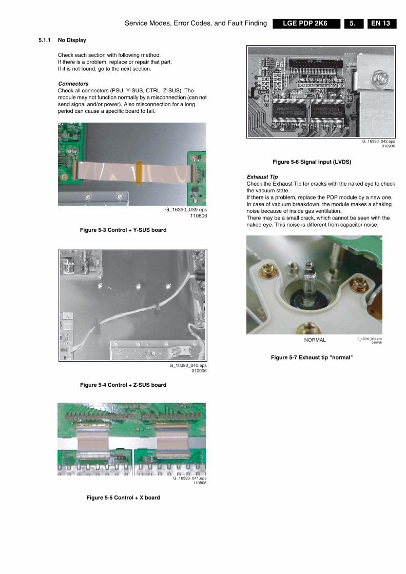
5.1.1 No Display
Check each section with following method. If there is a problem, replace or repair that part.If it is not found, go to the next section.
ConnectorsCheck all connectors (PSU, Y-SUS, CTRL, Z-SUS). The module may not function normally by a misconnection (can not send signal and/or power). Also misconnection for a long period can cause a specific board to fail.
Figure 5-3 Control + Y-SUS board
Figure 5-4 Control + Z-SUS board
Figure 5-5 Control + X board
Figure 5-6 Signal input (LVDS)
Exhaust TipCheck the Exhaust Tip for cracks with the naked eye to check the vacuum state.If there is a problem, replace the PDP module by a new one.In case of vacuum breakdown, the module makes a shaking noise because of inside gas ventilation.There may be a small crack, which cannot be seen with the naked eye. This noise is different from capacitor noise.
Figure 5-7 Exhaust tip "normal"
G_16390_039.eps110806
G_16390_040.eps010906
G_16390_041.eps110806
G_16390_042.eps010906
NORMAL F_15590_069.eps050705
Service Modes, Error Codes, and Fault FindingEN 14 LGE PDP 2K65.
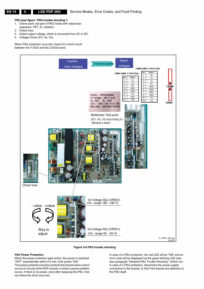
PSU (see figure “PSU trouble shooting“)1. Check each unit part of PSU inside with naked eye
(capacitor, FET, IC, resistor). 2. Check fuse.3. Check output voltage, which is converted from AC to DC.4. Voltage Check (5V, Va, Vs).
When PSU protection occurred: check for a short circuit between the Y-SUS and the Z-SUS board.
Figure 5-8 PSU trouble shooting
PSU Power ProtectionWhen the power protection gets active, the power is switched "OFF" automatically within 2-3 min. from power "ON".The power protection function protects the boards when a short occurs on circuits of the PDP module, or when a power problem occurs. If there is no power, even after replacing the PSU, find out where the short occurred.
In case of a PSU protection, the red LED will be "ON" and an error code will be displayed via the green blinking LED (see also paragraph "Detailed PSU Trouble Shooting", further on).In case of a PSU protection, disconnect the power supply connectors to the boards, to find if the boards are defective or the PSU itself.
if not the sameConfirm
input voltages
Adjust
voltages
- value +value
Check fuse
Way toadjust
Vs Voltage ADJ (VR551)(Vs : range 180 ~195 V)
Va Voltage ADJ (VR351)
(Va : range 55 ~ 65 V)
G_16391_007.eps030707
Multimeter Test point
(5V, Va ,Vs according to Module Label)
Service Modes, Error Codes, and Fault Finding EN 15LGE PDP 2K6 5.
5.1.2 Bar Defect (Vertical)
Check each section with the following method. If there is a problem, replace or repair that part. If not go to the next section.
ConnectorCheck the TCP connector and cables. If not connected well, it will result in a bar defect and abnormal display behaviour.
Figure 5-9 Connector check (1)
Figure 5-10 Connector check (2)
Checking the TCPConfirm whether the TCP was torn or chopped.
Figure 5-11 TCP torn
Figure 5-12 TCP IC broken
Control BoardThe Control board supplies the video signal to the TCP. So, if there is a bar defect on screen, it may be a Control board problem.
Figure 5-13 Control board address flow
5.1.3 Line Defect (Vertical)
In case of one line open or shorted, check for dirt (foreign substances) in TCP connector. First, try to remove the dirt with compressed air. If, after this, the same line appears again, replace the panel.
Line Open or ShortThis phenomenon is due to a TCP IC internal short or electrode problem. In this case, replace the panel.
Figure 5-14 Single line defect
Check here
Bar
F_15590_078.eps060705
Check here
Off
F_15590_079.eps060705
TCPtorn
F_15590_080.eps060705
TCP IC broken
F_15590_081.eps060705
F_15590_082.eps060705
Buffer IC
MCM
TCP
6 line
Array Resistor
192 Line output
R - array
1 line open
1 electrode open(on flex foil)
F_15590_083.eps060705
Service Modes, Error Codes, and Fault FindingEN 16 LGE PDP 2K65.
Line Open or Short with the Same DistanceThis is an MCM of Control board defect. The MCM cannot be replaced separately. So replace the Control board.
Figure 5-15 Evenly repeated lines
5.1.4 Bar Defect (Horizontal)
Most horizontal defects can be repaired. In case of adherence between a part of the film and the rear panel electrode, or a panel electrode open/short, replace the PDP panel.
ConnectorIf the connectors on the Y board and Z board are not plugged in well, it can result in a horizontal bar, because the sustain voltage cannot be supplied to the panel. So check the FPC connectors and YSUS<->YDRV first..
Figure 5-16 Check FPC connectors
Figure 5-17 Check drive connectors
Scan IC CheckCheck the diode value of the right side part of the output pin.
Figure 5-18 Scan IC output diode check
5.1.5 Line Defect (Horizontal)
FPC CheckIn case of one or more horizontal lines, this is probably due to FPC or panel inside the Control board. Y board is just normal.
Figure 5-19 Open FPC electrode / Panel electrode breakdown
G_16390_064.eps180806
MCM of CTRL board defect. MCM can not be replaced separately. So replace the CTRL board.
MCM (Multi Chip Module)
Horizontal bar
Disconnected
F_15590_085.eps060705
Disconnected
Screen off
F_15590_086.eps060705
Normal diode value= 0.6 (forward)F_15590_087.eps
060705
Normal diode value= OL (reverse)
Horizontal 1 line.
FPC electrode open
F_15590_089.eps070705
Panel electrodeInsulation break down
Service Modes, Error Codes, and Fault Finding EN 17LGE PDP 2K6 5.
Scan IC CheckCheck diode value of the right side part of the output pin.
Figure 5-20 Scan IC output diode check
5.1.6 Mis-discharge Defect
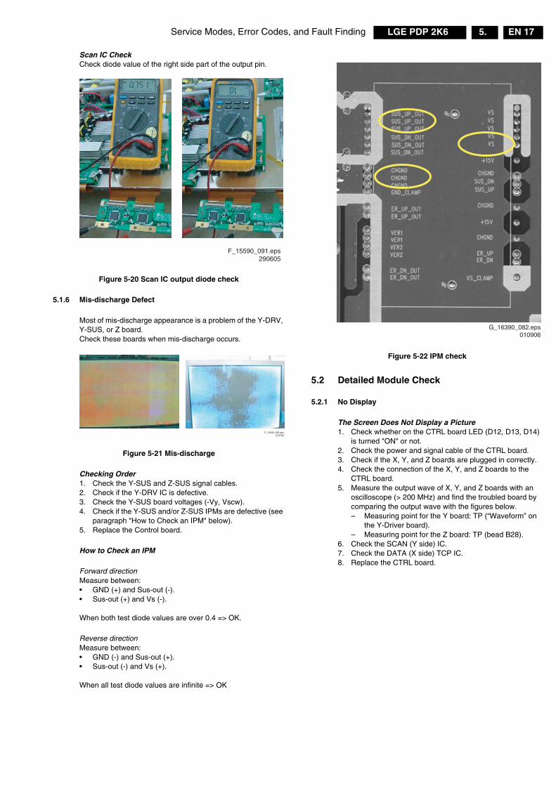
Most of mis-discharge appearance is a problem of the Y-DRV, Y-SUS, or Z board.Check these boards when mis-discharge occurs.
Figure 5-21 Mis-discharge
Checking Order1. Check the Y-SUS and Z-SUS signal cables.2. Check if the Y-DRV IC is defective.3. Check the Y-SUS board voltages (-Vy, Vscw).4. Check if the Y-SUS and/or Z-SUS IPMs are defective (see
paragraph "How to Check an IPM" below).5. Replace the Control board.
How to Check an IPM
Forward directionMeasure between:• GND (+) and Sus-out (-).• Sus-out (+) and Vs (-).
When both test diode values are over 0.4 => OK.
Reverse direction Measure between:• GND (-) and Sus-out (+).• Sus-out (-) and Vs (+).
When all test diode values are infinite => OK
Figure 5-22 IPM check
5.2 Detailed Module Check
5.2.1 No Display
The Screen Does Not Display a Picture1. Check whether on the CTRL board LED (D12, D13, D14)
is turned "ON" or not.2. Check the power and signal cable of the CTRL board.3. Check if the X, Y, and Z boards are plugged in correctly.4. Check the connection of the X, Y, and Z boards to the
CTRL board. 5. Measure the output wave of X, Y, and Z boards with an
oscilloscope (> 200 MHz) and find the troubled board by comparing the output wave with the figures below.– Measuring point for the Y board: TP (“Waveform” on
the Y-Driver board).– Measuring point for the Z board: TP (bead B28).
6. Check the SCAN (Y side) IC.7. Check the DATA (X side) TCP IC.8. Replace the CTRL board.
F_15590_091.eps290605
F_15590_093.eps070705
G_16390_082.eps010906
Service Modes, Error Codes, and Fault FindingEN 18 LGE PDP 2K65.
Figure 5-23 Output waveforms on X, Y, and Z-boards
G_16390_043.eps300806
Service Modes, Error Codes, and Fault Finding EN 19LGE PDP 2K6 5.
5.2.2 Display Defects
Half of the Screen is Not Shown• On the XR board:
1. Check if the power connector of the XR board is plugged in correctly.
2. Check if the 60-pin connection of the CTRL board to the XR board is plugged in correctly.
• On the XL board: 1. Check if the power connector of the XL board is
plugged in correctly.2. Check if the 60-pin connection of the CTRL board to
the XL board is plugged in correctly.• Replace relevant X board. Notes:Relationship between Screen and X board:
Figure 5-24 Screen display “1/2 display”
Vertical Parts of the Screen are Missing1. This can be related to a problem between the Data TCP
and the X board.2. Verify that the connector of the Data TCP is well connected
to the X board (it corresponds to the part of the screen that does not display the image).
3. Confirm whether the Data TCP fails (examination with the naked eye of blown ICs or other parts included).– If an IC is damaged: replace the panel.– In case of an X board short circuit or an open PWB
pattern: when the TCP IC is not defective, replace the X board.
Notes:• Example of screen display (any of the Data TCPs can be
shown).
Figure 5-25 Screen display “Vertical parts missing”
• How to examine the Data TCP IC– Connect [1] "Va Power" to the minus and [2] "GND" to
the plus of an ohmmeter, and then examine the diode in forward or reverse direction.
– Examine with the naked eye traces of blown ICs [3] or other parts.
Figure 5-26 Data TCP IC examination
Unusual Pattern on Display1. In case of generation of an unusual pattern of the Data TCP
IC unit as shown in the picture below, check the fixation of the relevant X board. If that doesn’t help, replace the X board.
2. In case of "Case 1":– Check the connection between the Data TCP
connector and the IC. – Replace the relevant X board, or the Control board.
3. In case of "Case 2" or "Case 3":– Check the connection between the CTRL board and
the relevant X board.– Replace the relevant X board or the CTRL board.
Note:• If the silicon tape between the X board and the heatsink
feels (partially) hard, it has to be replaced.
Figure 5-27 Possible cases
Scan FPC Problem1. Check the connection between Y DRV board and Scan
FPC. 2. If the Scan IC is defective, replace the Y DRV board.
Screen X-board
Left half of the screen Right X-board
Right half of the screen Left X-board
No imageImage
Left half of the screen Right half of the screen
G_16390_044.eps110806
F_15590_009.eps040705
All
Partial
Not at all
G_16390_081.eps010906
G_16390_045.eps140806
Case 1
Case 2
Case 3
Service Modes, Error Codes, and Fault FindingEN 20 LGE PDP 2K65.
Figure 5-28 Screen display “Scan FPC problem”
• Check method of the SCAN IC– Connect the Vpp pin to the plus and "GND" to the
minus of an ohmmeter, and then examine the diode in forward or reverse direction.
Figure 5-29 Scan IC
Vertical Lines with Regular Gap (Vertical Stripe Flash at Special Colour)• Replace the CTRL board.
Figure 5-30 Screen display “Vertical lines with regular gap”
Data Copy in Vertical Direction• Replace the Y-DRV board or the YSUS board.
Figure 5-31 Screen display “Data copy in vertical direction”
One or Several Vertical Line(s) on the Screen1. It may be caused by:
– Open or short circuit on DATA TCP FPC attached panel.
– Defect on DATA TCP IC attached panel.2. Replace the panel.
Figure 5-32 Screen display “Vertical lines”
One or Several Horizontal Lines on the Screen1. It may be caused by:
– Open or short circuit on SCAN FPC attached panel.– Defect on SCAN IC attached panel.
2. Replace the panel.
Figure 5-33 Screen display “Horizontal lines”
Low Brightness of Displayed Picture1. In this case, Z board operation is not complete. 2. Check the power cord of Z board.3. Check the connector of Z board and CTRL board. 4. Replace the CTRL board or Z board.
Partially Other Colour on Full White Screen or Partially Mis-Discharge on Full Black Screen.1. Check the Y board waveform, see below.2. Measure the output wave with an oscilloscope (> 200 MHz)
and compare the waveform with the waveform in the figure below. Adjust the Y board Set_up voltage (Vsetup) and time-interval “A” by changing VR3 and VR2.Check if -Vy and Vscan have been set correctly with VRy and VRsc respectively, to the value indicated on the voltage label. – Measuring Point for “Vsetup” and time-interval “A”:
Test point “Waveform” on the Y-Driver board.– Measuring Points for “-Vy” and “Vscan”:
Test points “Vy” and “Vsc” on the Y-SUS board.
One eighth of the screen
The screen display is poor
The screen display is good
G_16390_046.eps140806
F_15590_018.eps060605
F_15590_019.eps230407
Case 1: Entire CopyDisplay Pattern
Case 2: Top Copy Case 3: Bottom Copy Case 4: Entire Copy
(Input Signal)
G_16390_047.eps140806
It may show several vert.lines in a quarter or otherdivision part of screenincluding left case
F_15590_021.eps040705
F_15590_022.eps040705
It may show several horizontallines including left case
Service Modes, Error Codes, and Fault Finding EN 21LGE PDP 2K6 5.
Figure 5-34 Y output voltage waveform
No Specified Brightness at Specified Colour1. Check the connector of the CTRL board input signal
(LVDS).2. Replace the CTRL board.
5.2.3 Checking for Component Damage
Y IPM (IC 18) or Z IPM (IC 2)When the internal Sustain FET or ER FET of the Y IPM (IC18) or Z IPM (IC2) is damaged, there will be no picture, or the screen is partially mis-discharged.• Test Points: Waveform-GND (Y-DRV board), B28-GND (Z
board).• Wave format: Waveform (Y-DRV board) or B28 (Z board)
has no output wave.
Figure 5-35 IPM normal output
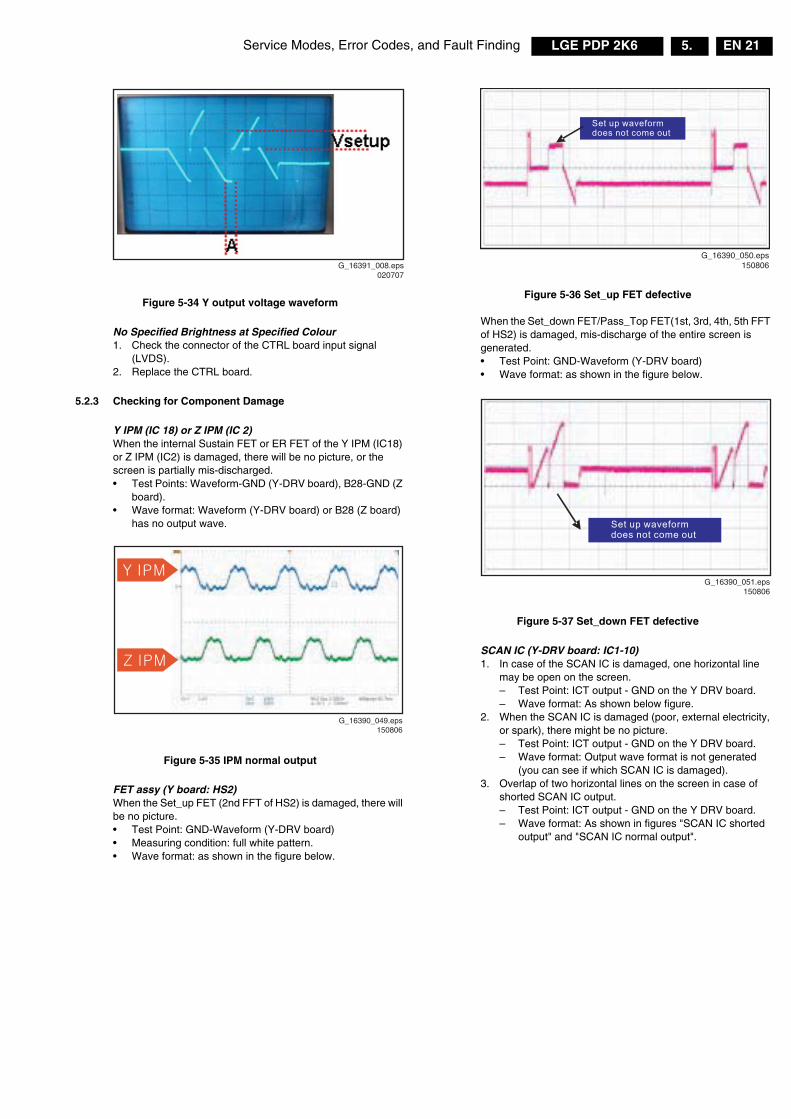
FET assy (Y board: HS2)When the Set_up FET (2nd FFT of HS2) is damaged, there will be no picture.• Test Point: GND-Waveform (Y-DRV board)• Measuring condition: full white pattern.• Wave format: as shown in the figure below.
Figure 5-36 Set_up FET defective
When the Set_down FET/Pass_Top FET(1st, 3rd, 4th, 5th FFT of HS2) is damaged, mis-discharge of the entire screen is generated.• Test Point: GND-Waveform (Y-DRV board)• Wave format: as shown in the figure below.
Figure 5-37 Set_down FET defective
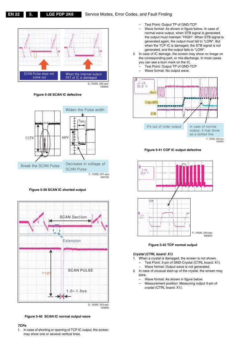
SCAN IC (Y-DRV board: IC1-10)1. In case of the SCAN IC is damaged, one horizontal line
may be open on the screen.– Test Point: ICT output - GND on the Y DRV board.– Wave format: As shown below figure.
2. When the SCAN IC is damaged (poor, external electricity, or spark), there might be no picture. – Test Point: ICT output - GND on the Y DRV board.– Wave format: Output wave format is not generated
(you can see if which SCAN IC is damaged).3. Overlap of two horizontal lines on the screen in case of
shorted SCAN IC output.– Test Point: ICT output - GND on the Y DRV board.– Wave format: As shown in figures "SCAN IC shorted
output" and "SCAN IC normal output".
G_16391_008.eps020707
G_16390_049.eps150806
G_16390_050.eps150806
Set up waveformdoes not come out
G_16390_051.eps150806
Set up waveformdoes not come out
Service Modes, Error Codes, and Fault FindingEN 22 LGE PDP 2K65.
Figure 5-38 SCAN IC defective
Figure 5-39 SCAN IC shorted output
Figure 5-40 SCAN IC normal output wave
TCPs1. In case of shorting or opening of TCP IC output, the screen
may show one or several vertical lines.
– Test Point: Output TP of GND-TCP– Wave format: As shown in figure below. In case of
normal wave output, when STB signal is generated, the output must maintain "HIGH". When STB signal is generated again, the output must fall to "LOW". But when the TCP IC is damaged, the STB signal is not generated, and the output falls to "LOW".
2. In case of IC damage, the screen may show no image on the corresponding part, or mis-discharge. In most cases you can see a burn mark on the IC.– Test Point: Output TP of GND-TCP– Wave format: No output wave.
Figure 5-41 COF IC output defective
Figure 5-42 TCP normal output
Crystal (CTRL board: X1)1. When a crystal is damaged, the screen is not shown.
– Test Point: 3-pin of GND-Crystal (CTRL board: X1).– Wave format: Output wave is not generated.
2. In case of unusual start-up of the crystal, the screen may blink.– Wave format: As shown in figure below.– Measurement position: Measuring output 3-pin of
crystal (CTRL board: X1).
G_16390_052.eps150806
7us
115V
7us
F_15590_031.eps040705
60V
G_16390_053.eps150806
’’
F_15590_033.eps060605
F_15590_034.eps060605
Service Modes, Error Codes, and Fault Finding EN 23LGE PDP 2K6 5.
Figure 5-43 Crystal normal output
Figure 5-44 Crystal defective output
F_15590_036.eps040705
F_15590_035.eps060605
Service Modes, Error Codes, and Fault FindingEN 24 LGE PDP 2K65.
5.3 Defect Description Form
This form must be used by the workshops for warranty claims:
Figure 5-45 Defect Description Form (DDF)
F_15590_115.eps050407
Defect Description Form LCD PLASMA v4.0 final Date last modified: 28/03/2006
To be filled in by WORKSHOP / WORK CENTER
Country:
Customer Account nr.:
Job sheet nr.:
PHILIPS
LCD & Plasma
DEFECT DESCRIPTION FORM
Type nr./Model nr. set
Serial nr. set
Type nr. display
Serial nr. display
Part nr display (12nc)
Return number
GE
NE
RA
L R
EP
AIR
DA
TA Condition
Symptom(s)
Constantly
Intermittently
After a while
In hot environment
In cold environment
Other:
No backlight
No picture
Picture too bright
Scratches (LCD only acc.Pixel criteria sheet V4.0)
Only partial picture
Unstable picture
Flickering / flashing picture
Lines across/down image
Inactive row(s)
Inactive column(s)
Missing colour(s)
Light leakage
Other:
PA
NE
L R
EP
AIR
PixelDefect(s):
Symptoms
Out of warranty
Dark dots
Bright dots
Qty of dots:
MarkDefect(s):
Thesesymptoms
are not claimable.
Following defect symptoms are out of warranty:
Broken glass / Broken polarizer
Scratch(es) on display / polarizer
Number of dark/bright pixels within spec.
Burn in (Plasma TV) / Sticking image (LCD TV)
MURA
-
-
-
-
-
BO
AR
D R
EP
AIR
Defect Board New Board
Spare Part Nr. Serial Nr. Spare Part Nr. Serial Nr.
1.
2.
3.
4.
Note 1: The defective LCD-panel / PDP needs to be returned in the same packaging as the new part was send. If not the warranty claim will be rejected.
Owner: PHILIPS CE EUROSERVICE
DE10WEG
Block Diagrams, Test Point Overviews, and Waveforms EN 25LGE PDP 2K6 6.
6. Block Diagrams, Test Point Overviews, and Waveforms
6.1 Block Diagram PDP Module
Figure 6-1 Block Diagram
7. Circuit Diagrams and PWB Layouts
Not applicable
Applied Voltage level is specified at the time when Full-White pattern is displayed on the panel.
Color PDP
1024 X 768 pixels
Address Driver
revirD nac
S
revi
rd n
i ats
us n
om
m oC
Vcc (5V)
Display data, Driver timing
MemoryController
DriverTimingController
InputInterfaceController
Va (60+1V)
Vs (175V~190V)
Controller
(External Power)
RA+RA-RB+
RD+RD-
RB-RC+RC-
RE+RE-
RCLK-RCLK+
(LVDS input)
I2C
G_16390_079.eps310806
AlignmentsEN 26 LGE PDP 2K68.
8. Alignments
Index of this chapter:8.1 General8.2 Alignments8.2.1 Tools8.2.2 Connection Diagram and Set-Up8.2.4 Y-SUS Alignment
8.1 General
Notes:• Important: if the PSU board, the Y-SUS board or the Z-
SUS board is replaced, the technician should check if the voltages delivered by these boards are correct. If not, the boards should be realigned in order to avoid bad performance of the PDP.
• Allow the set to warm up according conditions below for at least 10 minutes before adjusting.– Service signal: 100% Full White.– Service DC voltage: Vcc= 5 V, Va= 60 V, Vs= 180 V.– DC/DC Pack voltage: Vsc= 120 V, Vzb = 100 V, -Vy= -
1. First, set up the Vsc / -Vy voltage (Vsc= 120 V, -Vy= -200 V).
2. Then, adjust the voltage waveform (refer to adjustment).
Caution: Do not leave a still image for more than 10 minutes (especially The Digital pattern or Cross Hatch Pattern which has clear gradation) on the display, because this will cause burn-in effects.
8.2 Alignments
8.2.1 Tools
• Digital oscilloscope: > 200 MHz.• DVM (Digital Multimeter): Fluke 187 or similar.• Signal generator: VG-828 or similar.• DC power supply or PSU:
– 1 DC power supply for Vs: 0 - 200 V, > 10 A.– 1 DC power supply for Va: 0 - 100 V, > 5 A.– 1 DC power supply for 5V: 0 - 10 V, > 10 A.– A set of wires and appropriate connectors to hook up
the power supplies to the display.– Required voltage stability of the power supplies: within
± 1% for Vs and Va, within ± 3% for 5V.
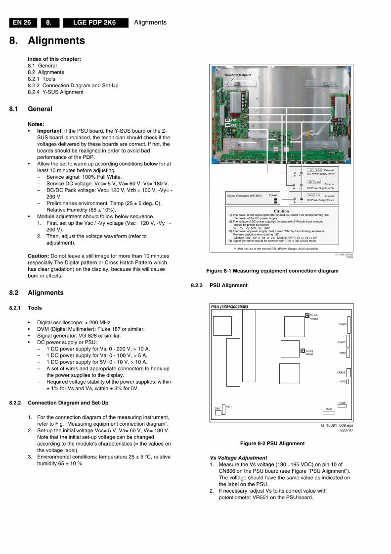
8.2.2 Connection Diagram and Set-Up
1. For the connection diagram of the measuring instrument, refer to Fig. "Measuring equipment connection diagram".
2. Set-up the initial voltage Vcc= 5 V, Va= 60 V, Vs= 180 V. Note that the initial set-up voltage can be changed according to the module’s characteristics (= the values on the voltage label).
3. Environmental conditions: temperature 25 ± 5 °C, relative humidity 65 ± 10 %.
Figure 8-1 Measuring equipment connection diagram
8.2.3 PSU Alignment
Figure 8-2 PSU Alignment
Vs Voltage Adjustment1. Measure the Vs voltage (180...195 VDC) on pin 10 of
CN806 on the PSU board (see Figure “PSU Alignment”). The voltage should have the same value as indicated on the label on the PSU.
2. If necessary, adjust Vs to its correct value with potentiometer VR551 on the PSU board.
180V 1.3A
DC Power Supply for Vs
65V 0.01A
DC Power Supply for Va
5V 1.2 A
DC Power Supply for 5V
Signal Generator (VG-825)
Power
Caution (1) The power of the signal generator should be turned “ON” before turning “ON”
the power of the DC power supply. (2) The voltage of DC power supplies, in standard of Module input voltage,
should be preset as follows: Vcc: 5V, Va: 60V, Vs: 180V
(3) The power of power supply must turned “ON” by the following sequence. Reverse direction when turning “off”.
* Module “ON” : 5V => Va => Vs, Module “OFF”: Vs => Va => 5V
(4) Signal generator should be selected with 1024 x 768 (XGA) mode.
Also the use of the normal PSU (Power Supply Unit) is possible
External
External
External
G_16390_023.eps170806
+ -
+ -
+ -
Waveform testpoint
VR2
VR3
G_16391_008.eps020707
PSU (3501Q00203B)
Z001F001
1M03
1M46
1M10
CN805
1M02
CN807
CN806
Vs adj
Va adj
VR551
VR351
G_16391_009.eps020707
Alignments EN 27LGE PDP 2K6 8.
Va Voltage Adjustment1. Measure the Va voltage (55...65 VDC) on pin 1 of CN806
on the PSU board (see Figure “PSU Alignment”). The voltage should have the same value as indicated on the label on the PSU.
2. If necessary, adjust Va to its correct value with potentiometer VR351 on the PSU board.
8.2.4 Y-SUS Alignment
Figure 8-3 Y-SUS alignment
Condition• Set up a situation as shown in “Measuring equipment
connection diagram”.• Check if the voltages Vs and Va of the PSU are correct
(see PSU label and PSU Alignment 8.2.3).
Vscan Voltage Adjustment1. Measure the Vscan voltage across C51 (or on the “Vsc”
test point on the right of connector P4) on the Y-SUS board (see Figure “Y-SUS Alignment”).
2. Adjust Vsc to the value indicated on the voltage sticker with potentiometer VRsc on the Y-SUS board.
-Vy Voltage Adjustment1. Measure the Vy voltage across R36 (or on the “Vy” test
point on the DC converter) on the Y-SUS board (see Figure “Y-SUS Alignment”).
2. Adjust -Vy to the value indicated on the voltage sticker with potentiometer VRy on the Y-SUS board.
Y -SUS Set-up Voltage Waveform AdjustmentNow connect the oscilloscope between the Waveform test point on the Y-Driver board and GND (see Figure ““Y-SUS Alignment”). Trigger with Vs-DA on the Control board (see Figure “Trigger point Vs-DA”).
Figure 8-4 Trigger point Vs-DA
Figure 8-5 V set-up waveform
1. Refer to Figure “V set-up waveform”.2. Adjust Vsetup to 150 ± 1 V with potentiometer VR3/Setup
on the Y-SUS board (see Figure “Y-SUS Alignment”).3. Adjust the duration of time-interval “A” to 10 ± 5 µsec with
potentiometer VR2/Setdown on the Y-SUS board.
G_16391_011.eps020707
Setup
Setdn
Vsc
-Vy
FS2
FS3
P1
P152P8
P2
P4
VR3
VR2
FS1
Waveform
P1
P2
P3
P4
P5
P6
P7
P8
C51R36
-VyVsc
VR
sc
VR
y
G_16391_012.eps020707
P7
P2
P1P11P10
P3
IC1X1
D13D14D15
P4
D12
CTRL board
VS_DA
TRIGGERPOINT
IC12
IC11
IC13
+1.8V
+3.3V
1
+3.3V
G_16391_008.eps020707
AlignmentsEN 28 LGE PDP 2K68.
8.2.5 Z-SUS Alignment
Figure 8-6 Z-SUS alignment
Condition• Set up a situation as shown in “Measuring equipment
connection diagram”.• Check if the voltages Vs and Va of the PSU are correct
(see PSU label and PSU Alignment 8.2.3).
Vzb (Z bias) Voltage Adjustment1. Measure the voltage between the Vzb test point (the drain
of Q18) and GND on the Z-SUS board (see Figure “Z-SUS Alignment”).
2. Adjust Vzb to 100 ± 0.5 V with potentiometerVRzb on the Z-SUS board.
8.2.6 Internal Test Patterns
The CTRL board is capable of generating its own video test patterns. To generate the test patterns, do as follows:• Disconnect the mains cord.• Disconnect the SSB of the TV set, by removing the cables
of connectors 1M03 and 1M46 on the PSU.• Reconnect the mains cord.• Connect pins 1 & 2 or pins 3 & 4 of Connector P1 on the
Control Board (see Figure below) to each other.• Now the internal test patterns are automatically shown in a
loop.
Figure 8-7 P1: Connector for Internal Test Patterns
G_16391_010.eps020707
B28
P4
P5
Q18
VRzb
P6
FS1
FS2
FS3
P1
P2
GND
Vzb
G_16391_012.eps020707
P7
P2
P1P11P10
P3
IC1X1
D13D14D15
P4
D12
CTRL board
VS_DA
TRIGGERPOINT
IC12
IC11
IC13
+1.8V
+3.3V
1
+3.3V
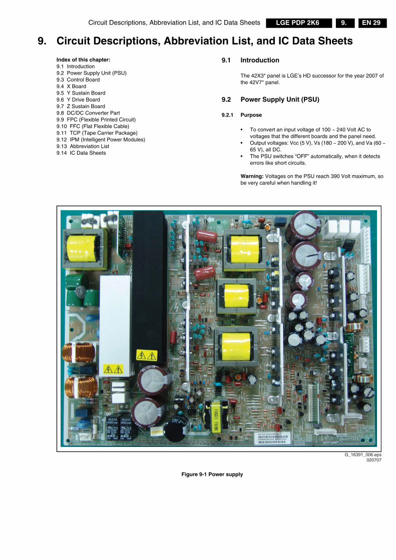
Circuit Descriptions, Abbreviation List, and IC Data Sheets EN 29LGE PDP 2K6 9.
9. Circuit Descriptions, Abbreviation List, and IC Data Sheets
Index of this chapter:9.1 Introduction9.2 Power Supply Unit (PSU)9.3 Control Board9.4 X Board9.5 Y Sustain Board9.6 Y Drive Board9.7 Z Sustain Board9.8 DC/DC Converter Part9.9 FPC (Flexible Printed Circuit)9.10 FFC (Flat Flexible Cable)9.11 TCP (Tape Carrier Package)9.12 IPM (Intelligent Power Modules)9.13 Abbreviation List9.14 IC Data Sheets
9.1 Introduction
The 42X3* panel is LGE’s HD successor for the year 2007 of the 42V7* panel.
9.2 Power Supply Unit (PSU)
9.2.1 Purpose
• To convert an input voltage of 100 ~ 240 Volt AC to voltages that the different boards and the panel need.
• Output voltages: Vcc (5 V), Vs (180 ~ 200 V), and Va (60 ~ 65 V), all DC.
• The PSU switches “OFF” automatically, when it detects errors like short circuits.
Warning: Voltages on the PSU reach 390 Volt maximum, so be very careful when handling it!
Figure 9-1 Power supply
G_16391_006.eps020707
Circuit Descriptions, Abbreviation List, and IC Data SheetsEN 30 LGE PDP 2K69.
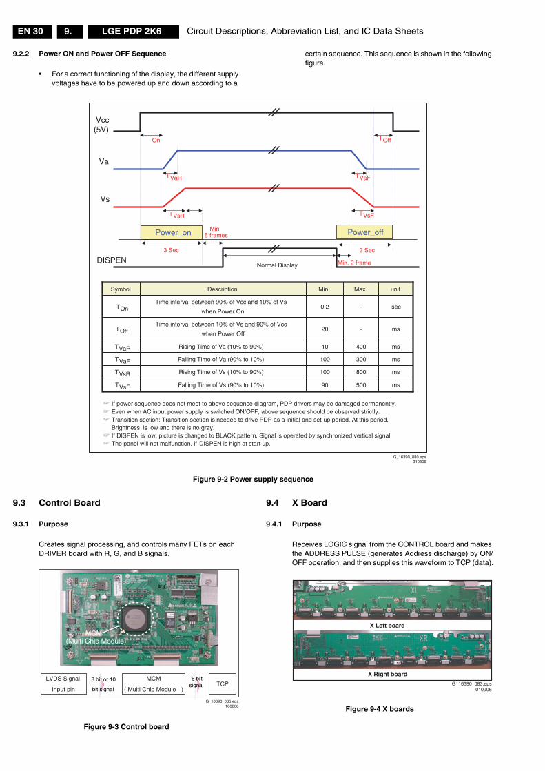
9.2.2 Power ON and Power OFF Sequence
• For a correct functioning of the display, the different supply voltages have to be powered up and down according to a
certain sequence. This sequence is shown in the following figure.
Figure 9-2 Power supply sequence
9.3 Control Board
9.3.1 Purpose
Creates signal processing, and controls many FETs on each DRIVER board with R, G, and B signals.
Figure 9-3 Control board
9.4 X Board
9.4.1 Purpose
Receives LOGIC signal from the CONTROL board and makes the ADDRESS PULSE (generates Address discharge) by ON/OFF operation, and then supplies this waveform to TCP (data).
Figure 9-4 X boards
G_16390_080.eps310806
If power sequence does not meet to above sequence diagram, PDP drivers may be damaged permanently.Even when AC input power supply is switched ON/OFF, above sequence should be observed strictly.Transition section: Transition section is needed to drive PDP as a initial and set-up period. At this period, Brightness is low and there is no gray.If DISPEN is low, picture is changed to BLACK pattern. Signal is operated by synchronized vertical signal.The panel will not malfunction, if DISPEN is high at start up.
Min. 2 frameNormal Display
Vcc(5V)
Va
Vs
DISPEN
TVaR
TVsR
TOn
TVaF
TVsF
TOff
ms800100Rising Time of Vs (10% to 90%)TVsR
ms300100Falling Time of Va (90% to 10%)TVaF
ms40010Rising Time of Va (10% to 90%)TVaR
ms50090Falling Time of Vs (90% to 10%)TVsF
ms-20Time interval between 10% of Vs and 90% of Vcc
when Power OffTOff
sec-0.2Time interval between 90% of Vcc and 10% of Vs
when Power OnTOn
unitMax.Min.DescriptionSymbol
Min.5 frames
3 Sec
Power_on
3 Sec
Power_off
MCM(Multi Chip Module)
LVDS Signal
Input pin
MCM
( Multi Chip Module )
6 bi tsignal
8 bit or 10
bit signalTCP
G_16390_035.eps100806
X Right board
G_16390_083.eps010906
X Left board
Circuit Descriptions, Abbreviation List, and IC Data Sheets EN 31LGE PDP 2K6 9.
9.5 Y Sustain Board
9.5.1 Purpose
Generates Sustain waveform, Reset, Vsc (Scan) and -Vy voltages, and supplies them to the Y DRIVE board.
Figure 9-5 Y Sustain board
9.5.2 Main Components
IPM, diodes, electrolytic capacitors, and FETs.
9.6 Y Drive Board
9.6.1 Purpose
• To supply Sustain, Reset waveform, made by the Y-SUS board, to the PDP through the SCAN DRIVER IC.
• To supply a waveform that selects the horizontal electrodes (Y SUSTAIN electrodes) sequentially.– Potential difference is 0 V between GND and Vpp of
the DRIVER IC during the SUSTAIN period.– Generates a potential difference between GND and
Vpp only during the SCAN period.
Figure 9-6 Y Drive board
9.7 Z Sustain Board
9.7.1 Purpose
To make the SUSTAIN and ERASE pulses that generate SUSTAIN discharge in the panel by receiving LOGIC signal from CONTROL board. This waveform is then supplied to the panel through FPC (Z).
9.7.2 Main Components
IPM, FET, DIODE, electrolytic capacitor, and E/R coil.
Figure 9-7 Z Sustain Board
* IPM (Intelligent Power Module)
E/R(Energy recovery)
G_16390_025.eps100806
•Y DRIVER
SCAN IC
Status separatedfrom Y-SUS Board
Assembled status
G_16390_036.eps100806
* IPM (Intelligent Power Module)
E/R(Energy recovery)
G_16390_026.eps100806
Circuit Descriptions, Abbreviation List, and IC Data SheetsEN 32 LGE PDP 2K69.
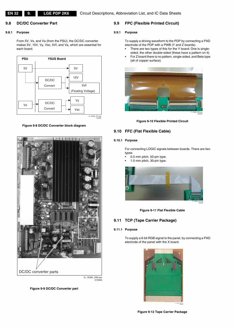
9.8 DC/DC Converter Part
9.8.1 Purpose
From 5V, Vs, and Va (from the PSU), the DC/DC converter makes 5V, 15V, Vy, Vsc, 5Vf, and Va, which are essential for each board.
Figure 9-8 DC/DC Converter block diagram
Figure 9-9 DC/DC Converter part
9.9 FPC (Flexible Printed Circuit)
9.9.1 Purpose
To supply a driving waveform to the PDP by connecting a PAD electrode of the PDP with a PWB (Y and Z boards).• There are two types of this for the Y board: One is single-
sided, the other double-sided (these have a pattern on it).• For Z board there is no pattern, single-sided, and Beta type
(all of copper surface).
Figure 9-10 Flexible Printed Circuit
9.10 FFC (Flat Flexible Cable)
9.10.1 Purpose
For connecting LOGIC signals between boards. There are two types• 0.5 mm pitch, 50-pin type.• 1.0 mm pitch, 30-pin type.
Figure 9-11 Flat Flexible Cable
9.11 TCP (Tape Carrier Package)
9.11.1 Purpose
To supply a 6-bit RGB signal to the panel, by connecting a PAD electrode of the panel with the X board.
Figure 9-12 Tape Carrier Package
PSU YSUS Board
5V 5V
15V
5Vf
(Floating Voltage)
Vs
Vy
Vsc
DC/DC
Convert
DC/DC
Convert
G_16390_037.eps100806
DC/DC converter partsG_16390_038.eps
010906
F_15590_058.eps200605
F_15590_059.eps200605
F_15590_060.eps200605
Circuit Descriptions, Abbreviation List, and IC Data Sheets EN 33LGE PDP 2K6 9.
9.12 IPM (Intelligent Power Modules)
9.12.1 Purpose
Attached to Y board (SUS IPM) and Z board (ER IPM): • SUS IPM generates the Sustain waveform• ER IPM performs an Energy Recovery function
Figure 9-13 Intelligent Power Modules
9.12.2 Main Components
Heatsink, capacitor, diode, IC, resistor, transistor, and FET.
9.13 Abbreviation List
AC Alternating CurrentB/D BoardCLK Clock signalCOF Chip On Flex / Foil / FilmCTRL Control (board)DC Direct CurrentFET Field Effect TransistorFPC Flexible Printed CircuitI/O Input/OutputIC Integrated CircuitIPM Intelligent Power ModuleLED Light Emitting DiodeLGE Lucky Goldstar Electronics (supplier)MCM Multi Chip ModulePCB Printed Circuit Board (same as PWB)PDP Plasma Display PanelPFC Power Factor Corrector circuitPSU Power Supply UnitPWB Printed Wiring Board (same as PCB)RGB Red, Green, Blue colour spaceSTB Stand-by signalTCP Tape Carrier Package
9.14 IC Data Sheets
Not applicable
* IPM (Intelligent Power Module)
E/R(Energy recovery)Y-SUS BOARD
* IPM (Intelligent Power Module)
E/R(Energy recovery)Z-SUS BOARD
G_16390_026.eps020707
Spare Parts ListEN 34 LGE PDP 2K610.
10. Spare Parts ListPlease refer to the Philips Service website, for an actual overview (monthly updated).
11. Revision ListManual xxxx xxx xxxx.0• First release.
Manual xxxx xxx xxxx.1• References in text and graphics to PSU model
3501Q00201A (not used in this PDP model) changed to references to PSU model 3501Q00203B.
• Corrections in texts referring to the PSU, Y-SUS and Z-SUS boards.
Manual xxxx xxx xxxx.2• Text on how to generate Internal Test Patterns added to
Chapter 8, Alignments.• Minor text corrections added.