21
16.575 – FPGA Logic Design Techniques Final Project Ryan Aldrich 1
| Date post: | 15-Apr-2017 |
| Category: |
Documents |
| Upload: | riddhi-shah |
| View: | 214 times |
| Download: | 9 times |

16.575 – FPGA Logic Design Techniques
Final Project
Ryan Aldrich
1

OBJECTIVE
The objective of this is to design the logic for an FPGA that will implement an analog clock with an hour hand and a minute hand that is displayed on a VGA screen. The design will implement the clock on a 480x480 matrix centered on a 640x480 display. The clock will update once per minute. Two switches connected to the FPGA will implement an Hour Increment and a Minute Increment button.
A timing diagram for a 640x480 VGA display is shown below. It shows the specific timing for VSYNC and HSYNC as well as their relative position. The table following the diagram contains the actual timing information relative to a 26.25 MHz clock.
2

BLOCK DIAGRAM
HARDWARE TEST
The source code fully synthesized and a design was able to be implemented. The programming file was downloaded to the board flash memory and tested via the VGA port. There was no display seen on the VGA monitor.
3

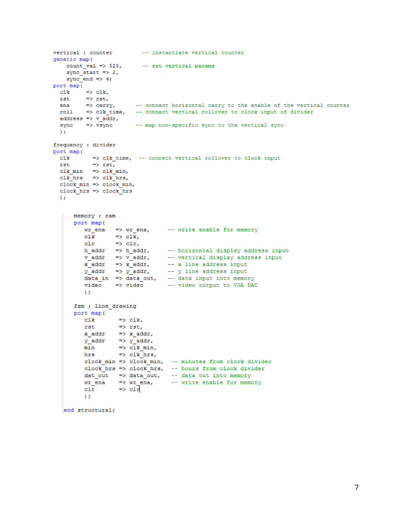
VHDL CODE – clock.vhd
4

5

6
VHDL CODE – counter.vhd
7
VHDL CODE – divider.vhd
8

VHDL CODE – ram.vhd
9

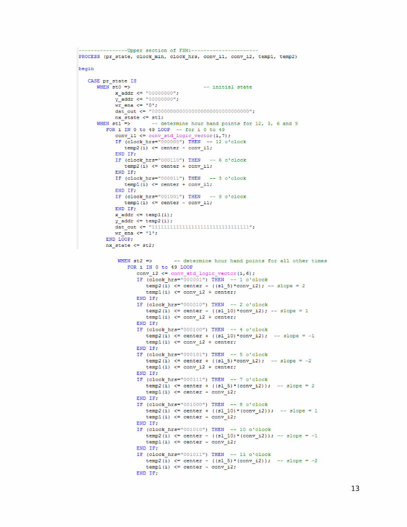
VHDL CODE – line_drawing.vhd
10

11

12
VHDL CODE – clock_tb.vhd
13

SIMULATION
Simulation results at the top level were unsuccessful and did not produce the desired hsync, vsync and video output.
14

Output of ram processes
15

Output of line drawing processes
16

Device Utilization Summary
Logic Utilization Used Available Utilization
Total Slice Registers 30 1,920 1%
Number used as Flip Flops 29
Number used as Latches 1
Number of 4 input LUTs 36 1,920 1%
Number of occupied Slices 31 960 3%
Number of slices containing only related logic
31 31 100%
Number of slices containing unrelated logic
0 31 0%
Total Number of 4 input LUTs 54 1,920 2%
Number used as logic 34
Number used as a route-thru 18
Number used for dual-port RAMs 2
Number of bonded IOBs 36 83 43%
Number of BUFGMUXs 1 24 4%
Average Fanout of Non-Clock Nets
3.27
17


