68
18-447: Computer Architecture Lecture 34: Emerging Memory Technologies Justin Meza (adapted from slides by Onur Mutlu) Carnegie Mellon University Spring 2013, 5/1/2013

18-447: Computer Architecture Lecture 34: Emerging Memory
Technologies
Justin Meza (adapted from slides by Onur Mutlu)
Carnegie Mellon University Spring 2013, 5/1/2013

The Main Memory System
n Main memory is a critical component of all computing systems: server, mobile, embedded, desktop, sensor
n Main memory system must scale (in size, technology, efficiency, cost, and management algorithms) to maintain performance growth and technology scaling benefits
2
Processor and caches
Main Memory Storage (SSD/HDD)

State of the Main Memory System n Recent technology, architecture, and application trends
q lead to new requirements from the memory system q exacerbate old requirements from the memory system
n DRAM alone is (will be) unlikely to satisfy all requirements
n Some emerging non-volatile memory technologies (e.g., PCM) appear promising to satisfy these requirements q and enable new opportunities
n We need to rethink the main memory system q to fix DRAM issues and enable emerging technologies q to satisfy all new and (exacerbated) old requirements
3
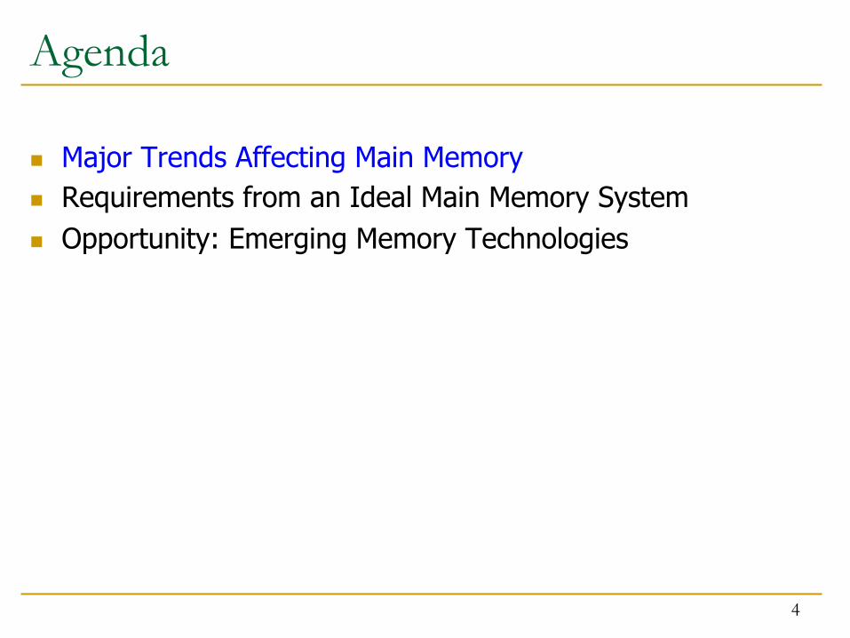
Agenda
n Major Trends Affecting Main Memory n Requirements from an Ideal Main Memory System n Opportunity: Emerging Memory Technologies
4

Major Trends Affecting Main Memory (I) n Need for main memory capacity and bandwidth increasing
n Main memory energy/power is a key system design concern
n DRAM technology scaling is ending
5

Demand for Memory Capacity n More cores è More concurrency è Larger working set
n Emerging applications are data-intensive
n Many applications/virtual machines (will) share main memory
q Cloud computing/servers: Consolidation to improve efficiency q GP-GPUs: Many threads from multiple parallel applications q Mobile: Interactive + non-interactive consolidation
6
IBM Power7: 8 cores Intel SCC: 48 cores AMD Barcelona: 4 cores

The Memory Capacity Gap
n Memory capacity per core expected to drop by 30% every two years
7
Core count doubling ~ every 2 years DRAM DIMM capacity doubling ~ every 3 years

Major Trends Affecting Main Memory (II) n Need for main memory capacity and bandwidth increasing
q Multi-core: increasing number of cores q Data-intensive applications: increasing demand/hunger for data q Consolidation: Cloud computing, GPUs, mobile
n Main memory energy/power is a key system design concern
n DRAM technology scaling is ending
8

Major Trends Affecting Main Memory (III) n Need for main memory capacity and bandwidth increasing
n Main memory energy/power is a key system design concern
q IBM servers: ~50% energy spent in off-chip memory hierarchy [Lefurgy, IEEE Computer 2003]
q DRAM consumes power when idle and needs periodic refresh
n DRAM technology scaling is ending
9

Major Trends Affecting Main Memory (IV) n Need for main memory capacity and bandwidth increasing
n Main memory energy/power is a key system design concern
n DRAM technology scaling is ending
q ITRS projects DRAM will not scale easily below 40nm q Scaling has provided many benefits:
n higher capacity, higher density, lower cost, lower energy
10

The DRAM Scaling Problem n DRAM stores charge in a capacitor (charge-based memory)
q Capacitor must be large enough for reliable sensing q Access transistor should be large enough for low leakage and high
retention time q Scaling beyond 40-35nm (2013) is challenging [ITRS, 2009]
n DRAM capacity, cost, and energy/power hard to scale
11

Trends: Problems with DRAM as Main Memory
n Need for main memory capacity and bandwidth increasing q DRAM capacity hard to scale
n Main memory energy/power is a key system design concern
q DRAM consumes high power due to leakage and refresh
n DRAM technology scaling is ending
q DRAM capacity, cost, and energy/power hard to scale
12

Agenda
n Major Trends Affecting Main Memory n Requirements from an Ideal Main Memory System n Opportunity: Emerging Memory Technologies
13

n Traditional q Enough capacity q Low cost q High system performance (high bandwidth, low latency)
n New q Technology scalability: lower cost, higher capacity, lower energy q Energy (and power) efficiency q QoS support and configurability (for consolidation)
14
Requirements from an Ideal Memory System

n Traditional q Higher capacity q Continuous low cost q High system performance (higher bandwidth, low latency)
n New q Technology scalability: lower cost, higher capacity, lower energy q Energy (and power) efficiency q QoS support and configurability (for consolidation)
15
Requirements from an Ideal Memory System
Emerging, resistive memory technologies (NVM) can help

Agenda
n Major Trends Affecting Main Memory n Requirements from an Ideal Main Memory System n Opportunity: Emerging Memory Technologies
16

The Promise of Emerging Technologies
n Likely need to replace/augment DRAM with a technology that is q Technology scalable q And at least similarly efficient, high performance, and fault-tolerant
n or can be architected to be so
n Some emerging resistive memory technologies appear promising q Phase Change Memory (PCM)? q Spin Torque Transfer Magnetic Memory (STT-MRAM)? q Memristors? q And, maybe there are other ones q Can they be enabled to replace/augment/surpass DRAM?
17

Agenda
n Major Trends Affecting Main Memory n Requirements from an Ideal Main Memory System n Opportunity: Emerging Memory Technologies
q Background q PCM (or Technology X) as DRAM Replacement q Hybrid Memory Systems
18

Charge vs. Resistive Memories
n Charge Memory (e.g., DRAM, Flash) q Write data by capturing charge Q q Read data by detecting voltage V
n Resistive Memory (e.g., PCM, STT-MRAM, memristors) q Write data by pulsing current dQ/dt q Read data by detecting resistance R
19

Limits of Charge Memory n Difficult charge placement and control
q Flash: floating gate charge q DRAM: capacitor charge, transistor leakage
n Reliable sensing becomes difficult as charge storage unit size reduces
20

Emerging Resistive Memory Technologies n PCM
q Inject current to change material phase q Resistance determined by phase
n STT-MRAM q Inject current to change magnet polarity q Resistance determined by polarity
n Memristors q Inject current to change atomic structure q Resistance determined by atom distance
21

What is Phase Change Memory? n Phase change material (chalcogenide glass) exists in two states:
q Amorphous: Low optical reflexivity and high electrical resistivity q Crystalline: High optical reflexivity and low electrical resistivity
22
PCM is resistive memory: High resistance (0), Low resistance (1) PCM cell can be switched between states reliably and quickly

How Does PCM Work? n Write: change phase via current injection
q SET: sustained current to heat cell above Tcryst q RESET: cell heated above Tmelt and quenched
n Read: detect phase via material resistance q amorphous/crystalline
23
Large Current
SET (cryst) Low resistance
103-104 Ω
Small Current
RESET (amorph) High resistance
Access Device
Memory Element
106-107 Ω
Photo Courtesy: Bipin Rajendran, IBM Slide Courtesy: Moinuddin Qureshi, IBM
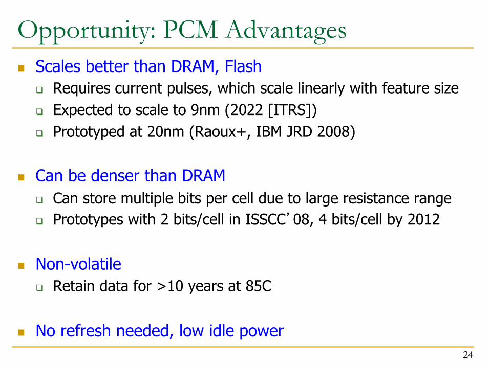
Opportunity: PCM Advantages n Scales better than DRAM, Flash
q Requires current pulses, which scale linearly with feature size q Expected to scale to 9nm (2022 [ITRS]) q Prototyped at 20nm (Raoux+, IBM JRD 2008)
n Can be denser than DRAM q Can store multiple bits per cell due to large resistance range q Prototypes with 2 bits/cell in ISSCC’08, 4 bits/cell by 2012
n Non-volatile q Retain data for >10 years at 85C
n No refresh needed, low idle power 24

Phase Change Memory Properties
n Surveyed prototypes from 2003-2008 (ITRS, IEDM, VLSI, ISSCC)
n Derived PCM parameters for F=90nm
n Lee, Ipek, Mutlu, Burger, “Architecting Phase Change Memory as a Scalable DRAM Alternative,” ISCA 2009.
25
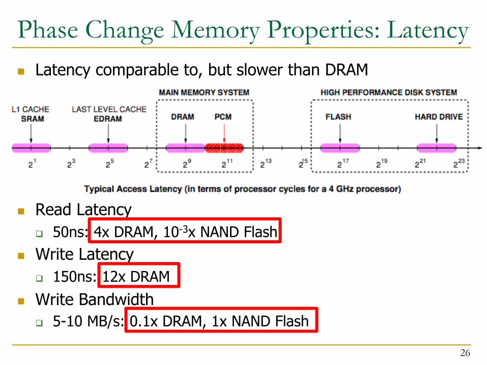
Phase Change Memory Properties: Latency n Latency comparable to, but slower than DRAM
n Read Latency
q 50ns: 4x DRAM, 10-3x NAND Flash
n Write Latency q 150ns: 12x DRAM
n Write Bandwidth q 5-10 MB/s: 0.1x DRAM, 1x NAND Flash
26
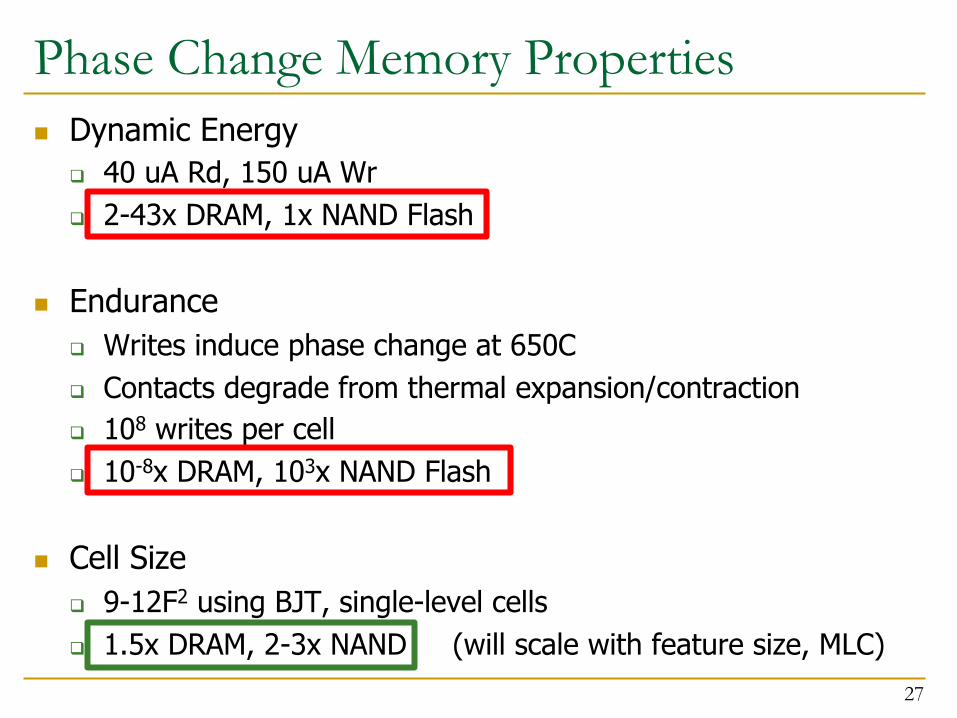
Phase Change Memory Properties n Dynamic Energy
q 40 uA Rd, 150 uA Wr q 2-43x DRAM, 1x NAND Flash
n Endurance q Writes induce phase change at 650C q Contacts degrade from thermal expansion/contraction q 108 writes per cell q 10-8x DRAM, 103x NAND Flash
n Cell Size q 9-12F2 using BJT, single-level cells q 1.5x DRAM, 2-3x NAND (will scale with feature size, MLC)
27

Phase Change Memory: Pros and Cons n Pros over DRAM
q Better technology scaling q Non volatility q Low idle power (no refresh)
n Cons q Higher latencies: ~4-15x DRAM (especially write) q Higher active energy: ~2-50x DRAM (especially write) q Lower endurance (a cell dies after ~108 writes)
n Challenges in enabling PCM as DRAM replacement/helper: q Mitigate PCM shortcomings q Find the right way to place PCM in the system q Ensure secure and fault-tolerant PCM operation
28
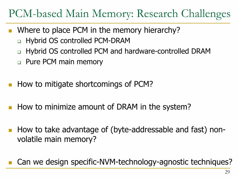
PCM-based Main Memory: Research Challenges n Where to place PCM in the memory hierarchy?
q Hybrid OS controlled PCM-DRAM q Hybrid OS controlled PCM and hardware-controlled DRAM q Pure PCM main memory
n How to mitigate shortcomings of PCM?
n How to minimize amount of DRAM in the system?
n How to take advantage of (byte-addressable and fast) non-volatile main memory?
n Can we design specific-NVM-technology-agnostic techniques? 29

PCM-based Main Memory (I) n How should PCM-based (main) memory be organized?
n Hybrid PCM+DRAM [Qureshi+ ISCA’09, Dhiman+ DAC’09, Meza+ IEEE CAL’12]: q How to partition/migrate data between PCM and DRAM
30

Hybrid Memory Systems: Research Challenges
n Partitioning q Should DRAM be a cache or main memory, or configurable? q What fraction? How many controllers?
n Data allocation/movement (energy, performance, lifetime) q Who manages allocation/movement? q What are good control algorithms? q How do we prevent degradation of service due to wearout?
n Design of cache hierarchy, memory controllers, OS q Mitigate PCM shortcomings, exploit PCM advantages
n Design of PCM/DRAM chips and modules q Rethink the design of PCM/DRAM with new requirements
31

PCM-based Main Memory (II) n How should PCM-based (main) memory be organized?
n Pure PCM main memory [Lee et al., ISCA’09, Top Picks’10]:
q How to redesign entire hierarchy (and cores) to overcome PCM shortcomings
32

Agenda
n Major Trends Affecting Main Memory n Requirements from an Ideal Main Memory System n Opportunity: Emerging Memory Technologies
q Background q PCM (or Technology X) as DRAM Replacement q Hybrid Memory Systems
33

An Initial Study: Replace DRAM with PCM n Lee, Ipek, Mutlu, Burger, “Architecting Phase Change
Memory as a Scalable DRAM Alternative,” ISCA 2009. q Surveyed prototypes from 2003-2008 (e.g. IEDM, VLSI, ISSCC) q Derived “average” PCM parameters for F=90nm
34

Results: Naïve Replacement of DRAM with PCM n Replace DRAM with PCM in a 4-core, 4MB L2 system n PCM organized the same as DRAM: row buffers, banks, peripherals n 1.6x delay, 2.2x energy, 500-hour average lifetime
n Lee, Ipek, Mutlu, Burger, “Architecting Phase Change Memory as a
Scalable DRAM Alternative,” ISCA 2009. 35
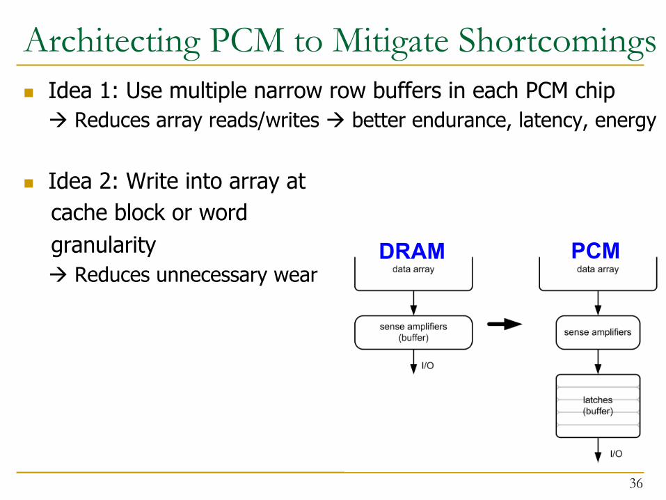
Architecting PCM to Mitigate Shortcomings n Idea 1: Use multiple narrow row buffers in each PCM chip
à Reduces array reads/writes à better endurance, latency, energy
n Idea 2: Write into array at cache block or word granularity
à Reduces unnecessary wear
36
DRAM PCM

Results: Architected PCM as Main Memory n 1.2x delay, 1.0x energy, 5.6-year average lifetime n Scaling improves energy, endurance, density
n Caveat 1: Worst-case lifetime is much shorter (no guarantees) n Caveat 2: Intensive applications see large performance and energy hits n Caveat 3: Optimistic PCM parameters?
37

Agenda
n Major Trends Affecting Main Memory n Requirements from an Ideal Main Memory System n Opportunity: Emerging Memory Technologies
q Background q PCM (or Technology X) as DRAM Replacement q Hybrid Memory Systems
38

Hybrid Memory Systems
Meza, Chang, Yoon, Mutlu, Ranganathan, “Enabling Efficient and Scalable Hybrid Memories,” IEEE Comp. Arch. Letters, 2012.
CPU DRAMCtrl
Fast, durable Small,
leaky, volatile, high-cost
Large, non-volatile, low-cost Slow, wears out, high active energy
PCM Ctrl DRAM Phase Change Memory (or Tech. X)
Hardware/software manage data allocation and movement to achieve the best of multiple technologies
(5-9 years of average lifetime)

One Option: DRAM as a Cache for PCM n PCM is main memory; DRAM caches memory rows/blocks
q Benefits: Reduced latency on DRAM cache hit; write filtering
n Memory controller hardware manages the DRAM cache q Benefit: Eliminates system software overhead
n Three issues: q What data should be placed in DRAM versus kept in PCM? q What is the granularity of data movement? q How to design a low-cost hardware-managed DRAM cache?
n Two idea directions: q Locality-aware data placement [Yoon+,ICCD’12]
q Cheap tag stores and dynamic granularity [Meza+,IEEE CAL’12]
40
Agenda
n Major Trends Affecting Main Memory n Requirements from an Ideal Main Memory System n Opportunity: Emerging Memory Technologies
q Background q PCM (or Technology X) as DRAM Replacement q Hybrid Memory Systems
n Row-Locality Aware Data Placement n Efficient DRAM (or Technology X) Caches
41
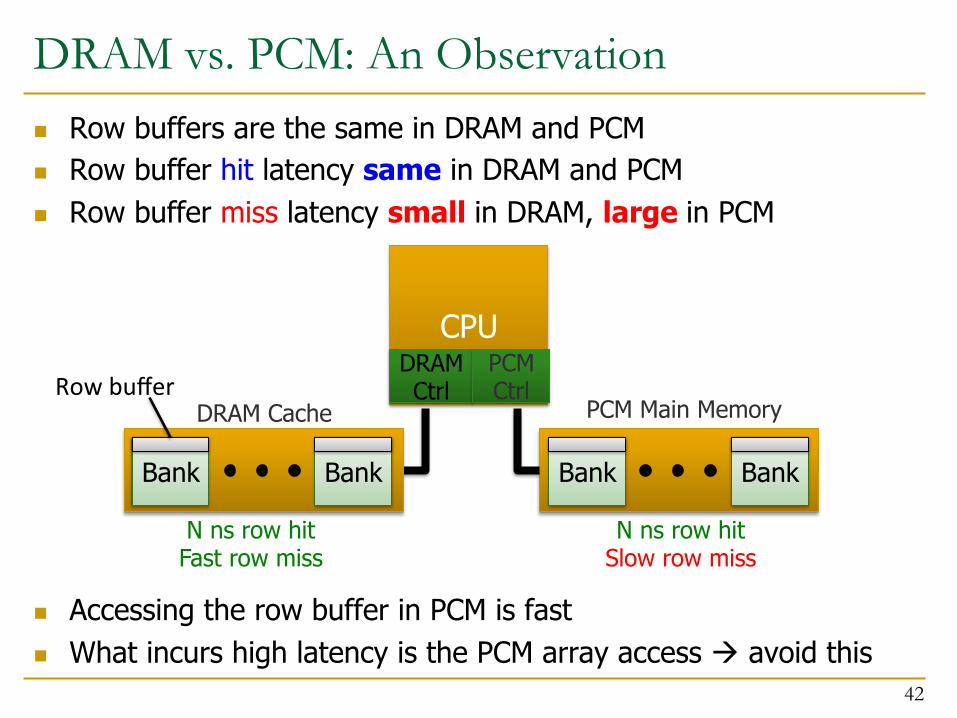
DRAM vs. PCM: An Observation n Row buffers are the same in DRAM and PCM n Row buffer hit latency same in DRAM and PCM n Row buffer miss latency small in DRAM, large in PCM
n Accessing the row buffer in PCM is fast n What incurs high latency is the PCM array access à avoid this
42
CPU DRAMCtrl
PCM Ctrl
Bank Bank Bank Bank
Row buffer DRAM Cache PCM Main Memory
N ns row hit Fast row miss
N ns row hit Slow row miss

Row-Locality-Aware Data Placement n Idea: Cache in DRAM only those rows that
q Frequently cause row buffer conflicts à because row-conflict latency is smaller in DRAM
q Are reused many times à to reduce cache pollution and bandwidth waste
n Simplified rule of thumb: q Streaming accesses: Better to place in PCM q Other accesses (with some reuse): Better to place in DRAM
n Bridges half of the performance gap between all-DRAM and all-PCM memory on memory-intensive workloads
n Yoon et al., “Row Buffer Locality Aware Caching Policies for Hybrid Memories,” ICCD, 2012.
43

Row-Locality-Aware Data Placement: Mechanism
n For a subset of rows in PCM, memory controller: q Tracks row conflicts as a predictor of future locality q Tracks accesses as a predictor of future reuse
n Cache a row in DRAM if its row conflict and access counts are greater than certain thresholds
n Determine thresholds dynamically to adjust to application/workload characteristics q Simple cost/benefit analysis every fixed interval
44

Evaluation Methodology n Core model
q 3-wide issue with 128-entry instruction window q 32 KB L1 D-cache per core q 512 KB L2 cache per core
n Memory model q 16 MB DRAM Cache / 512 MB PCM per core
n Scaled based on workload trace size and access patterns to be smaller than working set
q DDR3 800 MHz, single channel, 8 banks per device q Row buffer hit: 40 ns q Row buffer miss: 80 ns (DRAM); 128, 368 ns (PCM) q Cache data at 2 KB row granularity
45

Performance
46
0
0.2
0.4
0.6
0.8
1
1.2
1.4
Server Cloud Avg
No
rmal
ized
Wei
gh
ted
Sp
eed
up
Workload
FREQ RBLA RBLA-Dyn Reuse-aware RBL-aware RBL-aware (dynamic)

RBL-Aware Data Placement: Benefits n Benefit 1: Increased row buffer locality (RBL) in PCM by
moving low RBL data to DRAM
n Benefit 2: Reduced memory bandwidth consumption due to stricter caching criteria
n Benefit 3: Balanced memory request load between DRAM and PCM
47

n Heterogeneous DRAM cache + PCM memory with locality-aware data placement on a 16-core system
n Compared to all PCM main memory q 14% performance improvement
n Compared to an all DRAM main memory q Within 29% of performance
48
Row-Locality-Aware Data Placement: Results
Agenda
n Major Trends Affecting Main Memory n Requirements from an Ideal Main Memory System n Opportunity: Emerging Memory Technologies
q Background q PCM (or Technology X) as DRAM Replacement q Hybrid Memory Systems
n Row-Locality Aware Data Placement n Efficient DRAM (or Technology X) Caches
49

The Problem with Large DRAM Caches n A large DRAM cache requires a large metadata (tag +
block-based information) store n How do we design an efficient DRAM cache?
50
DRAM PCM
CPU
(small, fast cache) (high capacity)
Mem Ctlr
Mem Ctlr
LOAD X
Access X
Metadata: X à DRAM
X

Idea 1: Tags in Memory n Store tags in the same row as data in DRAM
q Store metadata in same row as their data q Data and metadata can be accessed together
n Benefit: No on-chip tag storage overhead n Downsides:
q Cache hit determined only after a DRAM access q Cache hit requires two DRAM accesses
51
Cache block 2 Cache block 0 Cache block 1 DRAM row
Tag0 Tag1 Tag2

Idea 2: Cache Tags in SRAM n Recall Idea 1: Store all metadata in DRAM
q To reduce metadata storage overhead
n Idea 2: Cache in on-chip SRAM frequently-accessed metadata q Cache only a small amount to keep SRAM size small
52

Idea 3: Dynamic Data Transfer Granularity n Some applications benefit from caching more data
q They have good spatial locality
n Others do not q Large granularity wastes bandwidth and reduces cache
utilization
n Idea 3: Simple dynamic caching granularity policy q Cost-benefit analysis to determine best DRAM cache block size q Group main memory into sets of rows q Some row sets follow a fixed caching granularity q The rest of main memory follows the best granularity
n Cost–benefit analysis: access latency versus number of cachings n Performed every quantum
53

TIMBER Tag Management n A Tag-In-Memory BuffER (TIMBER)
q Stores recently-used tags in a small amount of SRAM
n Benefits: If tag is cached: q no need to access DRAM twice q cache hit determined quickly
54
Tag0 Tag1 Tag2 Row0
Tag0 Tag1 Tag2 Row27
Row Tag
LOAD X
Cache block 2 Cache block 0 Cache block 1 DRAM row
Tag0 Tag1 Tag2

TIMBER Tag Management Example (I) n Case 1: TIMBER hit
55
Bank Bank Bank Bank
CPU
Mem Ctlr
Mem Ctlr
LOAD X
TIMBER: X à DRAM
X
Access X
Tag0 Tag1 Tag2 Row0
Tag0 Tag1 Tag2 Row27
TIMBER

TIMBER Tag Management Example (II) n Case 2: TIMBER miss
56
CPU
Mem Ctlr
Mem Ctlr
LOAD Y
Y à DRAM
Bank Bank Bank Bank
Access Metadata(Y)
Y
1. Access M(Y)
Tag0 Tag1 Tag2 Row0
Tag0 Tag1 Tag2 Row27
Miss
M(Y)
2. Cache M(Y)
Row143
3. Access Y (row hit)

Methodology n System: 8 out-of-order cores at 4 GHz
n Memory: 512 MB direct-mapped DRAM, 8 GB PCM q 128B caching granularity q DRAM row hit (miss): 200 cycles (400 cycles) q PCM row hit (clean / dirty miss): 200 cycles (640 / 1840 cycles)
n Evaluated metadata storage techniques q All SRAM system (8MB of SRAM) q Region metadata storage q TIM metadata storage (same row as data) q TIMBER, 64-entry direct-mapped (8KB of SRAM)
57

Metadata Storage Performance
58
0 0.1 0.2 0.3 0.4 0.5 0.6 0.7 0.8 0.9
1
SRAM Region TIM TIMBER
No
rmal
ized
Wei
gh
ted
S
pee
du
p
(Ideal)

0 0.1 0.2 0.3 0.4 0.5 0.6 0.7 0.8 0.9
1
SRAM Region TIM TIMBER
No
rmal
ized
Wei
gh
ted
S
pee
du
p
Metadata Storage Performance
59
-‐48%
Performance degrades due to increased metadata lookup access latency
(Ideal)

0 0.1 0.2 0.3 0.4 0.5 0.6 0.7 0.8 0.9
1
SRAM Region TIM TIMBER
No
rmal
ized
Wei
gh
ted
S
pee
du
p
Metadata Storage Performance
60
36%
Increased row locality reduces average
memory access latency
(Ideal)

0 0.1 0.2 0.3 0.4 0.5 0.6 0.7 0.8 0.9
1
SRAM Region TIM TIMBER
No
rmal
ized
Wei
gh
ted
S
pee
du
p
Metadata Storage Performance
61
23% Data with locality can access metadata at SRAM latencies
(Ideal)

0
0.1
0.2
0.3
0.4
0.5
0.6
0.7
0.8
0.9
1
SRAM Region TIM TIMBER TIMBER-Dyn
No
rmal
ized
Wei
gh
ted
Sp
eed
up
Dynamic Granularity Performance
62
10%
Reduced channel contenWon and
improved spaWal locality

0
0.1
0.2
0.3
0.4
0.5
0.6
0.7
0.8
0.9
1
SRAM Region TIM TIMBER TIMBER-‐Dyn
Normalized
Weighted Speedu
p TIMBER Performance
63
-‐6%
Reduced channel contenWon and
improved spaWal locality
Meza, Chang, Yoon, Mutlu, Ranganathan, “Enabling Efficient and Scalable Hybrid Memories,” IEEE Comp. Arch. Le_ers, 2012.

0
0.2
0.4
0.6
0.8
1
1.2
No
rmal
ized
Per
form
ance
per
W
att
(fo
r M
emo
ry S
yste
m)
TIMBER Energy Efficiency
64
Fewer migraWons reduce transmi_ed data and channel contenWon
18%
Meza, Chang, Yoon, Mutlu, Ranganathan, “Enabling Efficient and Scalable Hybrid Memories,” IEEE Comp. Arch. Le_ers, 2012.

Enabling and Exploiting NVM: Issues n Many issues and ideas from
technology layer to algorithms layer
n Enabling NVM and hybrid memory q How to tolerate errors? q How to enable secure operation? q How to tolerate performance and
power shortcomings? q How to minimize cost?
n Exploiting emerging tecnologies q How to exploit non-volatility? q How to minimize energy consumption? q How to exploit NVM on chip?
65
Microarchitecture
ISA
Programs
Algorithms Problems
Logic
Devices
Runtime System (VM, OS, MM)
User

Security Challenges of Emerging Technologies
1. Limited endurance à Wearout attacks 2. Non-volatility à Data persists in memory after powerdown à Easy retrieval of privileged or private information 3. Multiple bits per cell à Information leakage (via side channel)
66

Securing Emerging Memory Technologies
1. Limited endurance à Wearout attacks Better architecting of memory chips to absorb writes Hybrid memory system management Online wearout attack detection 2. Non-volatility à Data persists in memory after powerdown à Easy retrieval of privileged or private information Efficient encryption/decryption of whole main memory Hybrid memory system management 3. Multiple bits per cell à Information leakage (via side channel) System design to hide side channel information
67

Agenda
n Major Trends Affecting Main Memory n Requirements from an Ideal Main Memory System n Opportunity: Emerging Memory Technologies
q Background q PCM (or Technology X) as DRAM Replacement q Hybrid Memory Systems
68


