25
18‐447‐S18‐L16‐S1, James C. Hoe, CMU/ECE/CALCM, ©2018 18‐447 Lecture 16: Cache in Context (Uniprocessor) James C. Hoe Department of ECE Carnegie Mellon University
| Date post: | 29-May-2018 |
| Category: |
Documents |
| Upload: | phungthien |
| View: | 215 times |
| Download: | 0 times |

18‐447‐S18‐L16‐S1, James C. Hoe, CMU/ECE/CALCM, ©2018
18‐447 Lecture 16:Cache in Context (Uniprocessor)
James C. HoeDepartment of ECE
Carnegie Mellon University

18‐447‐S18‐L16‐S2, James C. Hoe, CMU/ECE/CALCM, ©2018
Housekeeping• Your goal today
– understand cache design and operation in context – focus on uniprocessor for now
• Notices– Lab 3, due next week– Handout #12 HW 4, due **Friday, 4/6, noon**– Midterm 2, Monday, 4/9– Final Exam, Thursday, 5/10, 1pm~4pm
• Readings– P&H Ch 5

18‐447‐S18‐L16‐S3, James C. Hoe, CMU/ECE/CALCM, ©2018
The Context
PC Instruction memory
4
Registers
M u x
M u x
M u x
ALU
EX
M
WB
M
WB
WB
ID/EX
0
EX/MEM
MEM/WB
Data memory
M u x
Hazard detection
unit
Forwarding unit
IF.Flush
IF/ID
Sign extend
Control
M u x
=
Shift left 2
M u x
[Based on original figure from P&H CO&D, COPYRIGHT 2004 Elsevier. ALL RIGHTS RESERVED.]

18‐447‐S18‐L16‐S4, James C. Hoe, CMU/ECE/CALCM, ©2018
Cache Interface for Dummies
Instruction memory
Instruction address
Instruction
MemRead
MemWrite
Data memory
Write data
Read data
Address
[Based on figures from P&H CO&D, COPYRIGHT 2004 Elsevier. ALL RIGHTS RESERVED.]
• Like the magic memory– present address, R/W command, etc– result or update valid after a short/fixed latency
• Except occasionally, cache needs more time– will become valid/ready eventually– what to do with pipeline until then? Stall!!
validvalid
ready

18‐447‐S18‐L16‐S5, James C. Hoe, CMU/ECE/CALCM, ©2018
Devil is in the detail

18‐447‐S18‐L16‐S6, James C. Hoe, CMU/ECE/CALCM, ©2018
Adding Caches to In‐order Pipeline• On I‐fetch and LW assuming 1‐cyc SRAM lookup
– if hit, just like magic memory– if miss, stall pipeline until cache ready
• On SW also assuming 1‐cycle SRAM lookup– if miss, stall pipeline until cache ready (must we??)– if hit, ???. . .
• For SW, need to check tag bank to ascertain hit before committing to write data bank– data bank write happens in the next cycle– if SW is followed immediately by LW
structural hazard stall

18‐447‐S18‐L16‐S7, James C. Hoe, CMU/ECE/CALCM, ©2018
Store Buffer• Why stall when memory port is usually free?• After tag bank hit, buffer SW address and data until next free data bank cycle – allow younger LW to execute (out‐of‐order)– must ensure SW target block not evicted
• Memory dependence and forwarding– younger LW must check against pending SW‐addresses in store buffer (CAM) for RAW dependence
store buffer w‐data
rw‐addrr‐dataaddr
data
youngest matching SW data
forwardif RAW
CAM

18‐447‐S18‐L16‐S8, James C. Hoe, CMU/ECE/CALCM, ©2018
Must wait for a miss? (uniprocessor)• In‐order pipeline must stall for LW‐miss• Younger instructions can move ahead of SW‐miss
– except LW to same address; if so, stall or forward – even additional SW‐misses to same and different addresses can be removed from “head‐of‐line”
• Modern out‐of‐order execution supports non‐blocking miss handling for both LW and SW– too expensive to stall (CPU/memory speed gap)– significant complexity in
• detecting and resolving memory dependencies• constructing precise exception state
18‐447‐S18‐L16‐S9, James C. Hoe, CMU/ECE/CALCM, ©2018
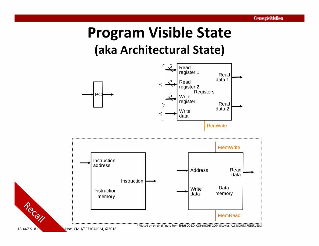
Program Visible State(aka Architectural State)
PC
Instruction memory
Instruction address
Instruction
MemRead
MemWrite
Data memory
Write data
Read data
Address
RegWrite
RegistersWrite register
Read data 1
Read data 2
Read register 1
Read register 2
Write data
5
5
5
**Based on original figure from [P&H CO&D, COPYRIGHT 2004 Elsevier. ALL RIGHTS RESERVED.]

18‐447‐S18‐L16‐S10, James C. Hoe, CMU/ECE/CALCM, ©2018
Harvard vs Princeton Architecture• Historically
– “Harvard” referred to Aiken’s Mark series with separate instruction and data memory
– “Princeton” referred to von Neumann’s unified instruction and data memory
• Contemporary usage: split vs unified “caches”• L1 I/D caches commonly split and asymmetrical
– double bandwidth and no‐cross pollution on disjoint I and D footprints
– I‐fetch smaller footprint, high‐spatial locality and read‐only I‐cache smaller, simpler
what about self‐modifying code?• L2 and L3 are unified for simplicity

18‐447‐S18‐L16‐S11, James C. Hoe, CMU/ECE/CALCM, ©2018
Multi‐Level Caches
L1‐I L1‐D
DRAM
‐ a few pclk latency‐many GB/sec on random word accesses
‐ hundreds of pclk latency‐ ~GB/sec on sequentialblock accesses
L2‐Unified
Intermediate cache levels bridge latency and bandwidth gap between L1 and DRAM
On‐chip oroff‐chip?

18‐447‐S18‐L16‐S12, James C. Hoe, CMU/ECE/CALCM, ©2018
Multi‐Level Cache Design• Upper‐level caches (L1)
– small C: upper‐bound by SRAM access time– smallish B: upper‐bound by C/B effects – a: required to counter C/B effects
• Lower‐level caches (L2, L3, etc.)– large C: upper‐bound by chip area– large B: to reduce tag storage overhead – a: upper bound by complexity and speed
• New very large (10s MB) on‐chip caches are highly associative (>10 ways)– same basic notions of ways and sets– but they don’t look or operate anything like “textbook”

18‐447‐S18‐L16‐S13, James C. Hoe, CMU/ECE/CALCM, ©2018
Write‐Through Cache• On write‐hit in Li, should Li+1be updated?• If yes, write‐through
– simple management– external agents (DMA and other proc’s) see up‐to‐date values in DRAM
• Write‐through to DRAM not viable today3.0GHz, IPC=2, 10% SW, ~8byte/SW ~5GB/sec
L1 write‐through to L2 still useful • With write‐through, on a write‐miss, should a cache block be allocated in Li (aka write‐allocate)?

18‐447‐S18‐L16‐S14, James C. Hoe, CMU/ECE/CALCM, ©2018
Write‐Back Cache• Hold changes in Li until block is displaced to Li+1
– on read or write miss, entire block is brought into Li– LWs and SWs hit in Li until replacement– on replacement, Li copy written back out to Li+1
adds latency to load miss stall• “Dirty” bit optimization
– keep per‐block status bit to track if a block has been modified since brought into Li
– if not dirty, no write‐back on replacement• What if a DMA device wants to read a DRAM location with a dirty cached copy?
How to find out? How to access?

18‐447‐S18‐L16‐S15, James C. Hoe, CMU/ECE/CALCM, ©2018
Write‐Back Cache and DMA• DRAM not always up‐to‐
date if write‐back• DMA should see up‐to‐date
value (aka, cache coherent)• Option 1: SW flushes whole
cache or specific blocks before programming DMA
• Option 2: cache monitors bus for external requests– ask request to a dirty location to “retry”
– write out dirty copy before request is repeated
Cache
DMA
Proc
DRAM
M[A]=X
c[A]={drty, X’}

18‐447‐S18‐L16‐S16, James C. Hoe, CMU/ECE/CALCM, ©2018
Cache and mmio• Loading from real memory location M[A] should return most recent value stored to M[A] writing M[A] once is the same as writing M[A] with same value multiple times in a row
reading M[A] multiple times returns same valueThis is why memory caching works!!
• LW/SW to mmap locations can have side‐effects– reading/writing mmap location can implycommands and other state changes
– consider a FIFO example• SW to 0xffff0000 pushes value• LW from 0xffff0000 returns popped value
FIFO
0xffff0000
What happens if 0xffff0000 is cached?

18‐447‐S18‐L16‐S17, James C. Hoe, CMU/ECE/CALCM, ©2018
Inclusion Principle• Classically, Li contents is always a subset of Li+1
– if an address is important enough to be in Li, it must be important enough to be in Li+1
– external agents (DMA and other proc’s) only have to check the lowest level to know if an address is cacheddo not need to consume L1 bandwidth
• Inclusion still common but no longer a given– nontrivial to maintain if Li+1 has lower associativity– too much redundant capacity in multicore with many per‐core Li and shared Li+1

18‐447‐S18‐L16‐S18, James C. Hoe, CMU/ECE/CALCM, ©2018
Inclusion Violation Example
x yx
y
x,y,z have same L1 idx bitsy,z have the same L2 idx bits
x,{y,z} have different L2 idx bits
step 1: L1 miss on z
step 2: x selected for eviction
2‐way set asso. L1
direct mapped L2
step 3: must evict y from L1 to replace y by z in L2
z
18‐447‐S18‐L16‐S19, James C. Hoe, CMU/ECE/CALCM, ©2018
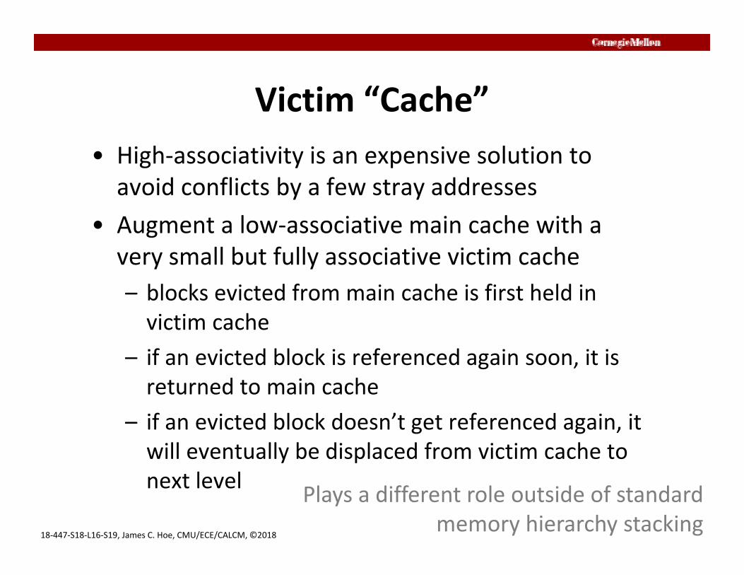
Victim “Cache”• High‐associativity is an expensive solution to avoid conflicts by a few stray addresses
• Augment a low‐associative main cache with a very small but fully associative victim cache– blocks evicted from main cache is first held in victim cache
– if an evicted block is referenced again soon, it is returned to main cache
– if an evicted block doesn’t get referenced again, it will eventually be displaced from victim cache to next level Plays a different role outside of standard
memory hierarchy stacking
18‐447‐S18‐L16‐S20, James C. Hoe, CMU/ECE/CALCM, ©2018
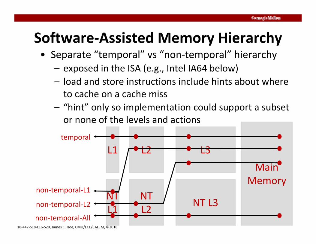
Software‐Assisted Memory Hierarchy• Separate “temporal” vs “non‐temporal” hierarchy
– exposed in the ISA (e.g., Intel IA64 below)– load and store instructions include hints about where to cache on a cache miss
– “hint” only so implementation could support a subset or none of the levels and actions
L1 L2 L3Main
MemoryNTL1
NTL2 NT L3
temporal
non‐temporal‐All
non‐temporal‐L1
non‐temporal‐L2
18‐447‐S18‐L16‐S21, James C. Hoe, CMU/ECE/CALCM, ©2018
Test yourself
Optional Reading: “Measuring Cache and TLB Performance and Their Effect on Benchmark Run Times,” Saavedra and Smith, 1995.

18‐447‐S18‐L16‐S22, James C. Hoe, CMU/ECE/CALCM, ©2018
What cache is in your computer?• How to figure out what cache configuration is in your computer– capacity (C), associativity (a), and block‐size (B)– number of levels
• The presence or lack of a cache should not be detectable by functional behavior of software
• But you could tell if you measured execution time to infer the number of cache misses

18‐447‐S18‐L16‐S23, James C. Hoe, CMU/ECE/CALCM, ©2018
Capacity Experiment: assume 2‐power C
• For increasing R = 1,2,4,8,16,…– allocate a buffer of size R– repeatedly read every byte in buffer in sequence– measure average read time in steadystate
• Analysis– for small R≤C, expect all reads to hit– for large R>C, expect reads to miss and detect corresponding jump in memory access time
• If continuing to increase R, read time jumps again when buffer size spills out to next cache levelWarning: timing won’t be perfect when you try this

18‐447‐S18‐L16‐S24, James C. Hoe, CMU/ECE/CALCM, ©2018
Block Size Experiment: knowing C• Allocate a buffer of size R >> C• For increasing S=1,2,4,8….,
– repeatedly read every S’th byte in buffer in sequence
– measure average read time in steadystate• Analysis
– since R>>C, expect first read to a block to miss when revisiting a block
– reads to same block in same round should hit– expect increasing average read time for increasing S until S≥B (no reuse in block)

18‐447‐S18‐L16‐S25, James C. Hoe, CMU/ECE/CALCM, ©2018
Associativity Experiment: knowing C• For increasing R, where R is a multiple of C
– allocate a buffer of size R– repeatedly read every C’th byte in buffer in sequence
• Analysis– all R/C references map to the same set– for small R s.t. R/C≤a, expect all reads to hit– for large R s.t. R/C>a, expect some reads to miss since touching more addresses than ways
note: 100% cache miss if LRU is used


![í ô r ð ð ó > µ î W Z/^ rs / v µ ] } v ^ Z ] µusers.ece.cmu.edu/~jhoe/course/ece447/S10handouts/L02.pdf · í ô r ð ð ó r^ î ì r> ì î r^ í ï U : u X , } U Dh l](https://static.documents.pub/doc/80x56/6059b4f2b5e57e200326ff97/-r-w-z-rs-v-v-z-usersececmuedujhoecourseece447s10handoutsl02pdf.jpg)


![í ô r ð ð ó > µ î ï W / o o µ ] À v } ( W o o o W ( } u vusers.ece.cmu.edu/~jhoe/course/ece447/S20handouts/L23.pdfí ô r ð ð ó r^ î ì r> î ï r^ í í U : u X , }](https://static.documents.pub/doc/80x56/5f032ab27e708231d407deba/-r-w-o-o-v-w-o-o-o-w-u-jhoecourseece447s20handoutsl23pdf.jpg)

