http://introcs.cs.princeton.edu ROBERT SEDGEWICK KEVIN WAYNE Computer Science C omputer S cience An Interdisciplinary Approach 19. Combinational Circuits COMPUTER SCIENCE SEDGEWICK/WAYNE PART II: ALGORITHMS, MACHINES, and THEORY Section 6.1 19. Combinational Circuits • Building blocks • Boolean algebra • Digital circuits • Adder circuit • Arithmetic/logic unit COMPUTER SCIENCE SEDGEWICK/WAYNE PART II: ALGORITHMS, MACHINES, and THEORY CS.19.A.Circuits.Basics Context Q. What is a combinational circuit? A. A digital circuit (all signals are 0 or 1) with no feedback (no loops). 3 Q. Why combinational circuits? A. Accurate, reliable, general purpose, fast, cheap. Applications. Smartphone, tablet, game controller, antilock brakes, microprocessor, … Basic abstractions • On and off. • Wire: propagates on/off value. • Switch: controls propagation of on/off values through wires. analog circuit: signals vary continuously sequential circuit: loops allowed (stay tuned) 4 Wires Wires propagate on/off values • ON (1): connected to power. • OFF (0): not connected to power. • Any wire connected to a wire that is ON is also ON. • Drawing convention: "flow" from top, left to bottom, right. power connection 1 thick wires are ON 1 1 thin wires are OFF 0
Transcript
http://introcs.cs.princeton.edu
R O B E R T S E D G E W I C K K E V I N W A Y N E
Com
puter Science
ComputerScience
An Interdisciplinary Approach
19. Combinational Circuits
COMPUTER SC I ENCE S E D G E W I C K / W A Y N E
PART I I : ALGORITHMS, MAC HINES , and THEORY
Section 6.1
19. Combinational Circuits
•Building blocks •Boolean algebra •Digital circuits •Adder circuit •Arithmetic/logic unit
COMPUTER SC I ENCE S E D G E W I C K / W A Y N E
PART I I : ALGORITHMS, MAC HINES , and THEORY
CS.19.A.Circuits.Basics
Context
Q. What is a combinational circuit?
A. A digital circuit (all signals are 0 or 1) with no feedback (no loops).
3
Q. Why combinational circuits?
A. Accurate, reliable, general purpose, fast, cheap.
Applications. Smartphone, tablet, game controller, antilock brakes, microprocessor, …
Basic abstractions
• On and off.
• Wire: propagates on/off value.
• Switch: controls propagation of on/off values through wires.
Wires propagate on/off values • ON (1): connected to power. • OFF (0): not connected to power. • Any wire connected to a wire that is ON is also ON. • Drawing convention: "flow" from top, left to bottom, right.
powerconnection
1
thick wires are ON
1
1
thin wires are OFF
0
5
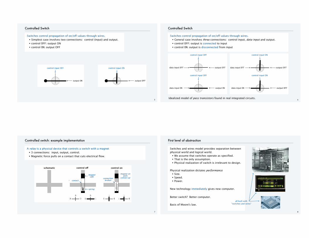
Switches control propagation of on/off values through wires. • Simplest case involves two connections: control (input) and output. • control OFF: output ON • control ON: output OFF
Controlled Switch
control input OFF
output ON
control input ON
output OFF
6
Switches control propagation of on/off values through wires. • General case involves three connections: control input, data input and output. • control OFF: output is connected to input • control ON: output is disconnected from input
Controlled Switch
control input OFF
control input OFF control input ON
control input ON
data input OFF output OFF
data input ON output ON
data input OFF output OFF
data input ON output OFF
Idealized model of pass transistors found in real integrated circuits.
7
A relay is a physical device that controls a switch with a magnet • 3 connections: input, output, control. • Magnetic force pulls on a contact that cuts electrical flow.
Controlled switch: example implementation
schematicschematicschematicschematic control off control on
contactconnection
broken
magnet on pulls
contact upmagnet
(off )
spring
First level of abstraction
Switches and wires model provides separation between physical world and logical world. • We assume that switches operate as specified. • That is the only assumption. • Physical realization of switch is irrelevant to design.
•Building blocks •Boolean algebra •Digital circuits •Adder circuit •Arithmetic/logic unit
COMPUTER SC I ENCE S E D G E W I C K / W A Y N E
PART I I : ALGORITHMS, MAC HINES , and THEORY
CS.19.B.Circuits.Algebra
Boolean algebra
Developed by George Boole in 1840s to study logic problems • Variables represent true or false (1 or 0 for short). • Basic operations are AND, OR, and NOT (see table below).
Widely used in mathematics, logic and computer science.
A truth table is a systematic way to define a Boolean function • One row for each possible set of arguments. • Each row gives the function value for the specified arguments. • N inputs: 2N rows needed.
AND
x y xy
0 0 0
0 1 0
1 0 0
1 1 1
OR
x y x + y
0 0 0
0 1 1
1 0 1
1 1 1
XOR
x y XOR
0 0 0
0 1 1
1 0 1
1 1 0
NOR
x y NOR
0 0 1
0 1 0
1 0 0
1 1 0
NOT
x x'
0 1
1 0
16
Truth table proofs
Truth tables are convenient for establishing identities in Boolean logic • One row for each possibility. • Identity established if columns match.
x y xy(xy )
'
0 0 0 1
0 1 0 1
1 0 0 1
1 1 1 0
x y x' y' x ' + y '
0 0 1 1 1
0 1 1 0 1
1 0 0 1 1
1 1 0 0 0
Proofs of DeMorgan's laws
x y x + y(x + y ) '
0 0 0 1
0 1 1 0
1 0 1 0
1 1 1 0
x y x' y' x 'y '
0 0 1 1 1
0 1 1 0 0
1 0 0 1 0
1 1 0 0 0
(xy ) ' = (x ' + y ' ) (x + y) ' = x'y'
NOR NOR
17
All Boolean functions of two variables
x y ZERO AND x y XOR OR NOR EQ ¬y ¬x NAND ONE
0 0 0 0 0 0 0 0 0 0 1 1 1 1 1 1 1 1
0 1 0 0 0 0 1 1 1 1 0 0 0 0 1 1 1 1
1 0 0 0 1 1 0 0 1 1 0 0 1 1 0 0 1 1
1 1 0 1 0 1 0 1 0 1 0 1 0 1 0 1 0 1
Q. How many Boolean functions of two variables?
A. 16 (all possibilities for the 4 bits in the truth table column).
Truth tables for all Boolean functions of 2 variables
18
Functions of three and more variables
x y z AND OR NOR MAJ ODD
0 0 0 0 0 1 0 0
0 0 1 0 1 0 0 1
0 1 0 0 1 0 0 1
0 1 1 0 1 0 1 0
1 0 0 0 1 0 0 1
1 0 1 0 1 0 1 0
1 1 0 0 1 0 1 0
1 1 1 1 1 0 1 1
Q. How many Boolean functions of three variables?
A. 256 (all possibilities for the 8 bits in the truth table column).
•Building blocks •Boolean algebra •Digital circuits •Adder circuit •Arithmetic/logic unit
COMPUTER SC I ENCE S E D G E W I C K / W A Y N E
PART I I : ALGORITHMS, MAC HINES , and THEORY
CS.19.C.Circuits.Digital
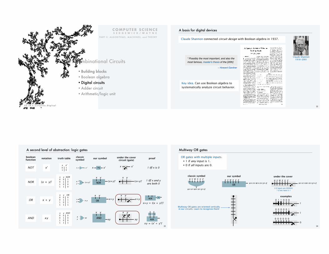
A basis for digital devices
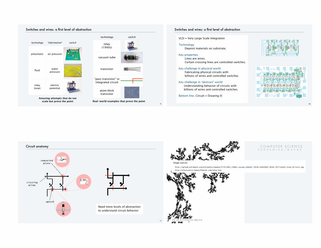
Claude Shannon connected circuit design with Boolean algebra in 1937.
22
Claude Shannon 1916�2001“ Possibly the most important, and also the
most famous, master's thesis of the [20th]
− Howard Gardner
Key idea. Can use Boolean algebra to systematically analyze circuit behavior.
23
x y NOR0 0 10 1 01 0 01 1 0
x y OR0 0 00 1 11 0 11 1 1
x y AND0 0 00 1 01 0 01 1 1
x x'0 11 0
truth table
NOT
boolean function notation
x '
NOR (x + y )'
OR x + y
AND xy
under the cover circuit (gate)
proof
1 iff x is 0
1 iff x and y are both 0
A second level of abstraction: logic gates
x+y = ((x + y )')'
NOR ¬
xy = (x ' + y ')'
NOR
¬ ¬
classic symbol our symbol
¬x x'
AND
x y
xy
OR
x yx+y
NOR
x y(x+y )'(x+y )'
x x'
yx(x+y )'
yxx+y
xy
x y
24
Multiway OR gates
OR gates with multiple inputs. • 1 if any input is 1. • 0 if all inputs are 0.
classic symbol u v w x y z
u+v+w+x+y+z 0 if inputs are 000000; 1 if any input is 1
our symbol
u+v+w+x+y+zu v w x y z
OR
examples0 1 1 0 0 0
1
0 0 0 0 0 1 1
0 0 0 0 0 0
0
Multiway OR gates are oriented verticallyin our circuits. Learn to recognize them!
under the coveru v w x y z
u+v+w+x+y+z
25
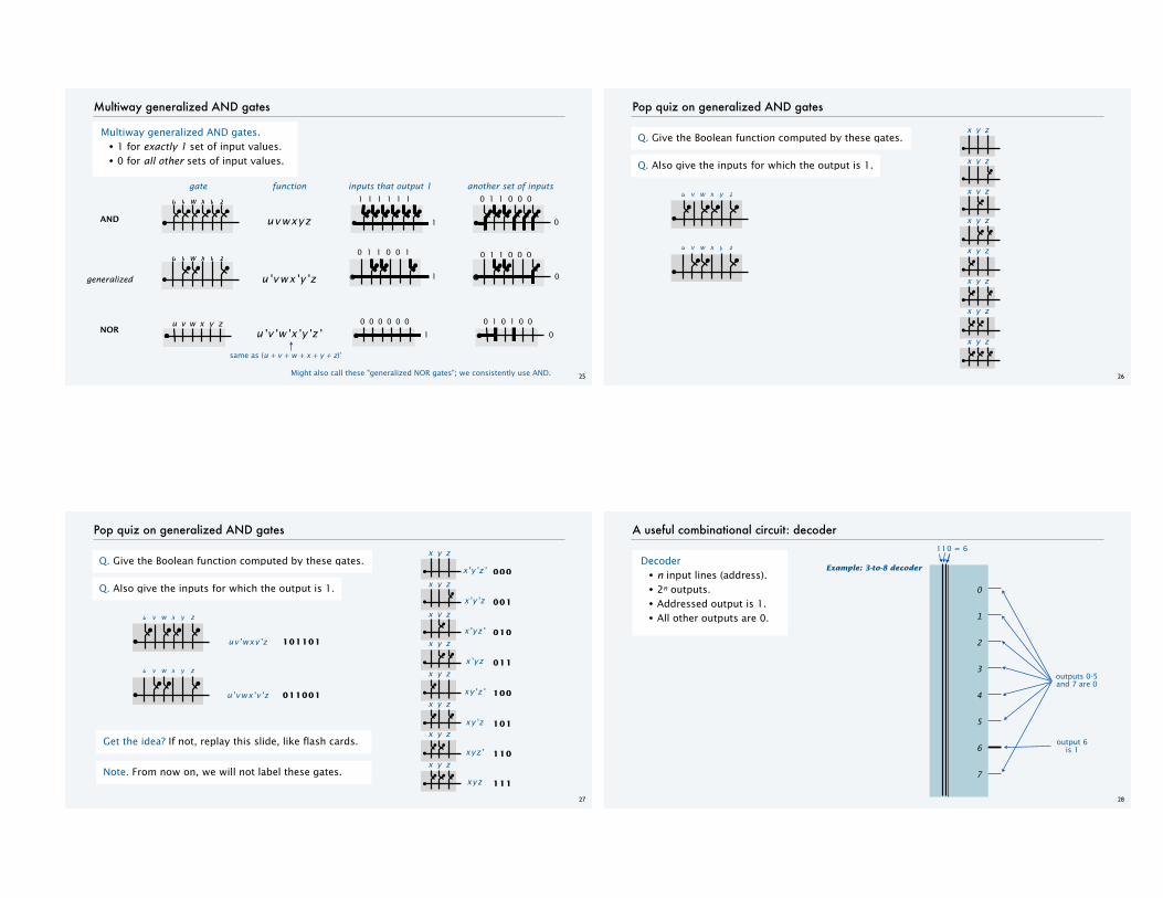
Multiway generalized AND gates
Multiway generalized AND gates. • 1 for exactly 1 set of input values. • 0 for all other sets of input values.
generalized
u v w x y z
u 'vwx'y 'z
NORu v w x y z 0 0 0 0 0 0
1
0 1 0 1 0 0
0
0 1 1 0 0 0
01
0 1 1 0 0 1
u'v 'w 'x 'y 'z '
same as (u + v + w + x + y + z)'
Might also call these "generalized NOR gates"; we consistently use AND.
1 1 1 1 1 1
1
inputs that output 1
AND
u v x y zw
uvwxyz
gate function0 1 1 0 0 0
0
another set of inputs
Pop quiz on generalized AND gates
26
Q. Give the Boolean function computed by these gates.
Q. Also give the inputs for which the output is 1.
x y z
x y z
x y z
x y z
x y z
x y z
x y z
x y z
u v w x y z
u w x y zv
Pop quiz on generalized AND gates
27
Q. Give the Boolean function computed by these gates.
Q. Also give the inputs for which the output is 1.
x y z
x y z
x y z
x y z
x y z
x y z
x y z
x y z
u v w x y z
u w x y zv
Note. From now on, we will not label these gates.
Get the idea? If not, replay this slide, like flash cards.
xyz 111
xyz ' 110
xy 'z 101
xy 'z ' 100
x 'yz 011
x 'yz ' 010
x 'y 'z 001
x 'y 'z ' 000
u'vwx'y 'z 011001
uv 'wxy 'z 101101
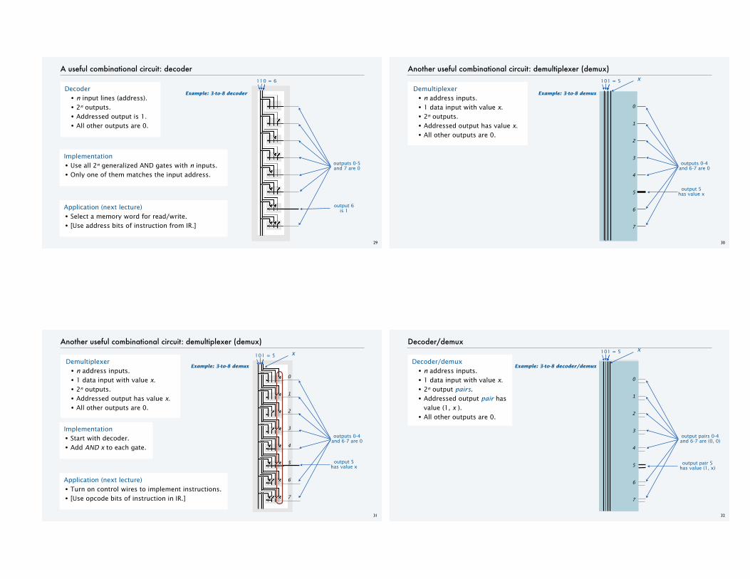
A useful combinational circuit: decoder
Decoder • n input lines (address). • 2n outputs. • Addressed output is 1. • All other outputs are 0.
28
110 = 6
0
1
2
3
4
5
6
7
output 6 is 1
Example: 3-to-8 decoder
outputs 0-5 and 7 are 0
29
A useful combinational circuit: decoder
Implementation • Use all 2n generalized AND gates with n inputs. • Only one of them matches the input address.
110 = 6
Application (next lecture) • Select a memory word for read/write. • [Use address bits of instruction from IR.]
Decoder • n input lines (address). • 2n outputs. • Addressed output is 1. • All other outputs are 0.
Example: 3-to-8 decoder
output 6 is 1
outputs 0-5 and 7 are 0
Another useful combinational circuit: demultiplexer (demux)
Demultiplexer • n address inputs. • 1 data input with value x. • 2n outputs. • Addressed output has value x. • All other outputs are 0.
30
101 = 5 x
output 5 has value x
outputs 0-4 and 6-7 are 0
0
1
2
3
4
5
6
7
Example: 3-to-8 demux
Another useful combinational circuit: demultiplexer (demux)
Demultiplexer • n address inputs. • 1 data input with value x. • 2n outputs. • Addressed output has value x. • All other outputs are 0.
31
101 = 5 x
Implementation • Start with decoder. • Add AND x to each gate.
Application (next lecture) • Turn on control wires to implement instructions. • [Use opcode bits of instruction in IR.]
output 5 has value x
outputs 0-4 and 6-7 are 0
0
1
2
3
4
5
6
7
Example: 3-to-8 demux
32
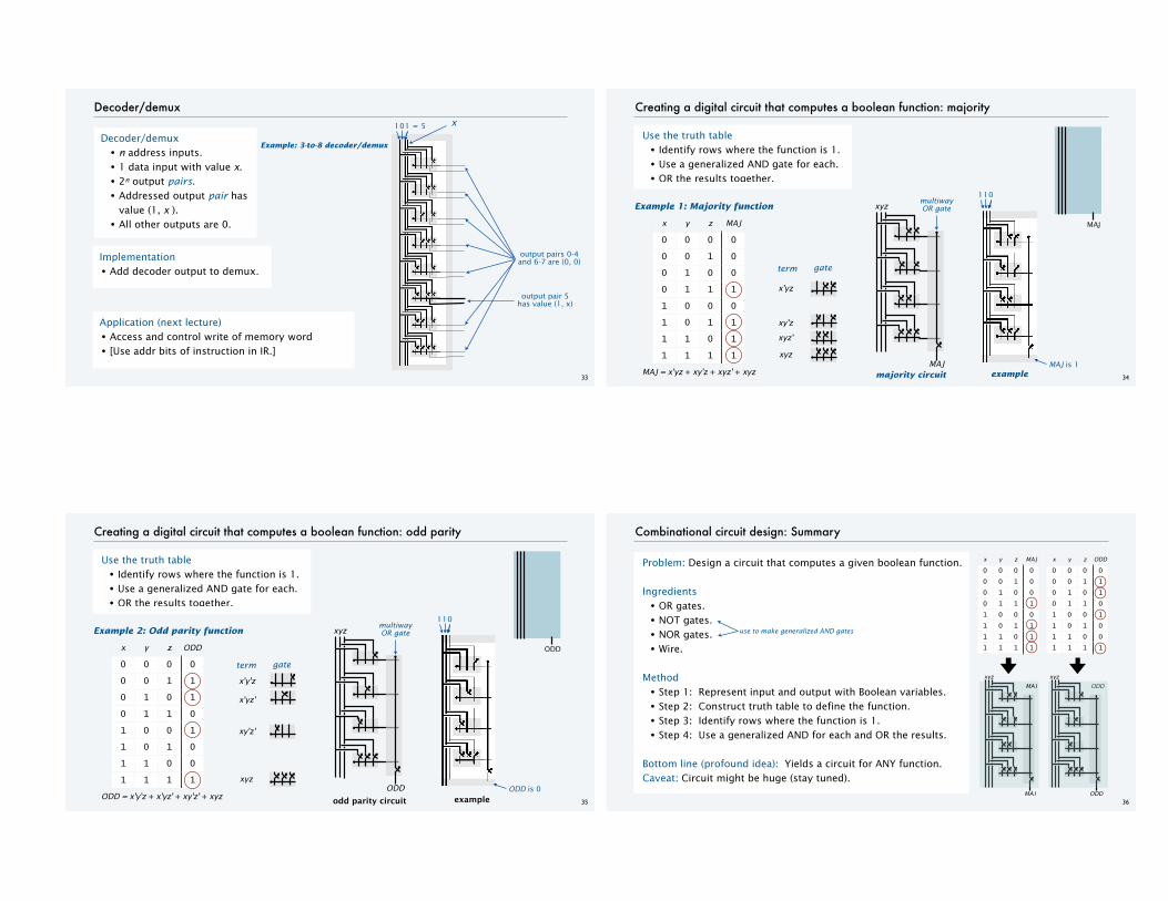
Decoder/demux101 = 5 x
output pair 5 has value (1, x)
output pairs 0-4 and 6-7 are (0, 0)
0
1
2
3
4
5
6
7
Decoder/demux • n address inputs. • 1 data input with value x. • 2n output pairs. • Addressed output pair has
value (1, x ). • All other outputs are 0.
Example: 3-to-8 decoder/demux
33
Decoder/demux
Implementation • Add decoder output to demux.
Application (next lecture) • Access and control write of memory word • [Use addr bits of instruction in IR.]
Decoder/demux • n address inputs. • 1 data input with value x. • 2n output pairs. • Addressed output pair has
value (1, x ). • All other outputs are 0.
101 = 5 x
output pair 5 has value (1, x)
output pairs 0-4 and 6-7 are (0, 0)
Example: 3-to-8 decoder/demux
34
Creating a digital circuit that computes a boolean function: majority
Use the truth table • Identify rows where the function is 1. • Use a generalized AND gate for each. • OR the results together.
x y z MAJ
0 0 0 0
0 0 1 0
0 1 0 0
0 1 1 1
1 0 0 0
1 0 1 1
1 1 0 1
1 1 1 1
MAJ = x'yz + xy'z + xyz' + xyz
xy'z
xyz'
xyz
Example 1: Majority function
MAJ
xyz
majority circuit example
110
MAJ is 1
x'yz
gateterm
multiway OR gate
MAJ
35
Creating a digital circuit that computes a boolean function: odd parity
Use the truth table • Identify rows where the function is 1. • Use a generalized AND gate for each. • OR the results together.
x y z ODD
0 0 0 0
0 0 1 1
0 1 0 1
0 1 1 0
1 0 0 1
1 0 1 0
1 1 0 0
1 1 1 1
ODD = x'y'z + x'yz' + xy'z' + xyz
110
exampleODD is 0
xyz
xy'z'
x'yz'
x'y'z
gateterm
ODD
ODD
xyz
odd parity circuit
multiway OR gateExample 2: Odd parity function
36
Combinational circuit design: Summary
Problem: Design a circuit that computes a given boolean function.
Ingredients • OR gates. • NOT gates. • NOR gates. • Wire.
Method • Step 1: Represent input and output with Boolean variables. • Step 2: Construct truth table to define the function. • Step 3: Identify rows where the function is 1. • Step 4: Use a generalized AND for each and OR the results.
Bottom line (profound idea): Yields a circuit for ANY function. Caveat: Circuit might be huge (stay tuned).
x y z ODD
0 0 0 0
0 0 1 1
0 1 0 1
0 1 1 0
1 0 0 1
1 0 1 0
1 1 0 0
1 1 1 1
x y z MAJ
0 0 0 0
0 0 1 0
0 1 0 0
0 1 1 1
1 0 0 0
1 0 1 1
1 1 0 1
1 1 1 1
MAJ
xyz
MAJ
ODD
xyz
ODD
use to make generalized AND gates
37
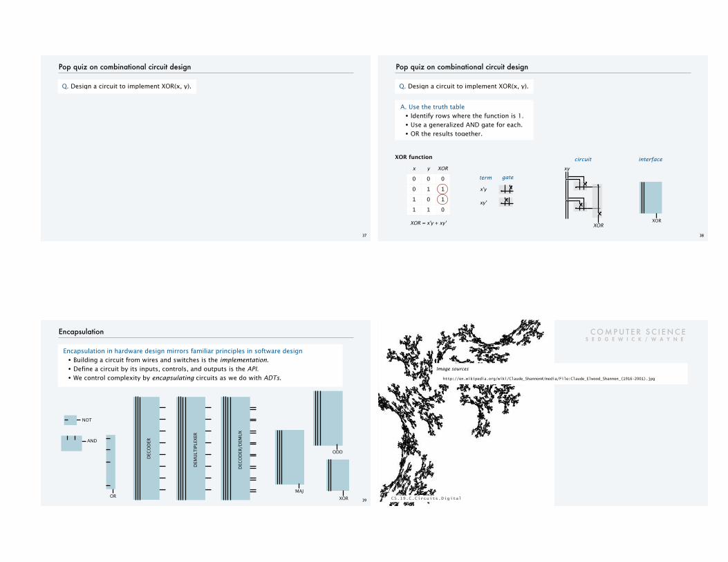
Pop quiz on combinational circuit design
Q. Design a circuit to implement XOR(x, y).
38
Pop quiz on combinational circuit design
A. Use the truth table • Identify rows where the function is 1. • Use a generalized AND gate for each. • OR the results together.
XOR = x'y + xy'
x y XOR
0 0 0
0 1 1
1 0 1
1 1 0
XOR function
xy'
Q. Design a circuit to implement XOR(x, y).
xy
XOR
circuit
x'y
term gate
interface
XOR
39
Encapsulation
Encapsulation in hardware design mirrors familiar principles in software design • Building a circuit from wires and switches is the implementation. • Define a circuit by its inputs, controls, and outputs is the API. • We control complexity by encapsulating circuits as we do with ADTs.
DEC
OD
ER
DEM
ULT
IPLE
XER
MAJ
ODD
XOROR
NOT
AND
DEC
OD
ER/D
EMU
X
C O M P U T E R S C I E N C E S E D G E W I C K / W A Y N E
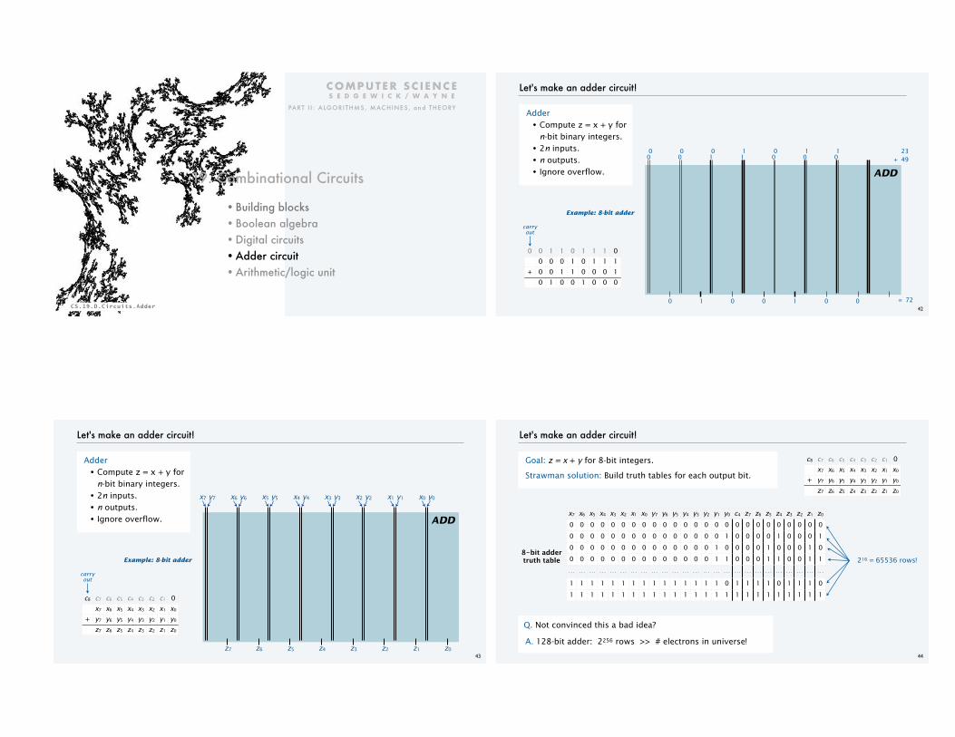
A. 128-bit adder: 2256 rows >> # electrons in universe!
216 = 65536 rows!
c8 c7 c6 c5 c4 c3 c2 c1 0x7 x6 x5 x4 x3 x2 x1 x0
+ y7 y6 y5 y4 y3 y2 y1 y0
z7 z6 z5 z4 z3 z2 z1 z0
45
Let's make an adder circuit!
Goal: z = x + y for 8-bit integers.
Do one bit at a time. • Build truth table for carry bit. • Build truth table for sum bit.
xi yi ci ci+1
0 0 0 0
0 0 1 0
0 1 0 0
0 1 1 1
1 0 0 0
1 0 1 1
1 1 0 1
1 1 1 1
carry bit
xi yi ci zi
0 0 0 0
0 0 1 1
0 1 0 1
0 1 1 0
1 0 0 1
1 0 1 0
1 1 0 0
1 1 1 1
sum bit
MAJ
0
0
0
1
0
1
1
1
ODD
0
1
1
0
1
0
0
1
A surprise! • Carry bit is MAJ. • Sum bit is ODD.
c8 c7 c6 c5 c4 c3 c2 c1 0x7 x6 x5 x4 x3 x2 x1 x0
+ y7 y6 y5 y4 y3 y2 y1 y0
z7 z6 z5 z4 z3 z2 z1 z0
46
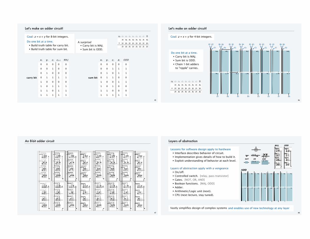
Let's make an adder circuit!
Goal: z = x + y for 4-bit integers.
x7 y7 x6 y6 x5 y5 x4 y4 x3 y3 x2 y2 x1 y1 x0 y0
z7 z6 z5 z4 z3 z2 z1 z0
c8 c7 c6 c5 c4 c3 c2 c1 0x7 x6 x5 x4 x3 x2 x1 x0
+ y7 y6 y5 y4 y3 y2 y1 y0
z7 z6 z5 z4 z3 z2 z1 z0
Do one bit at a time. • Carry bit is MAJ. • Sum bit is ODD. • Chain 1-bit adders
to "ripple" carries.
c7 c6 c5 c4 c3 c2 c1 c0
47
An 8-bit adder circuit
48
Layers of abstraction
Lessons for software design apply to hardware • Interface describes behavior of circuit. • Implementation gives details of how to build it. • Exploit understanding of behavior at each level.
Layers of abstraction apply with a vengeance • On/off. • Controlled switch. [relay, pass transistor] • Gates. [NOT, OR, AND] • Boolean functions. [MAJ, ODD] • Adder. • Arithmetic/Logic unit (next). • CPU (next lecture, stay tuned).
Vastly simplifies design of complex systems
NOT OR AND
and enables use of new technology at any layer
MAJ ODD
ADD
C O M P U T E R S C I E N C E S E D G E W I C K / W A Y N E
CS.19.D.Circuits.Adder
19. Combinational Circuits
•Building blocks •Boolean algebra •Digital circuits •Adder circuit •Arithmetic/logic unit
COMPUTER SC I ENCE S E D G E W I C K / W A Y N E
PART I I : ALGORITHMS, MAC HINES , and THEORY
CS.19.E.Circuits.ALU
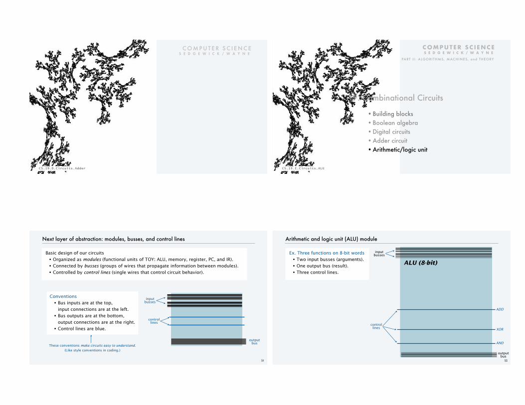
Next layer of abstraction: modules, busses, and control lines
Basic design of our circuits • Organized as modules (functional units of TOY: ALU, memory, register, PC, and IR). • Connected by busses (groups of wires that propagate information between modules). • Controlled by control lines (single wires that control circuit behavior).
51
Conventions • Bus inputs are at the top,
input connections are at the left. • Bus outputs are at the bottom,
output connections are at the right. • Control lines are blue.
These conventions make circuits easy to understand. (Like style conventions in coding.)
output bus
input busses
control lines
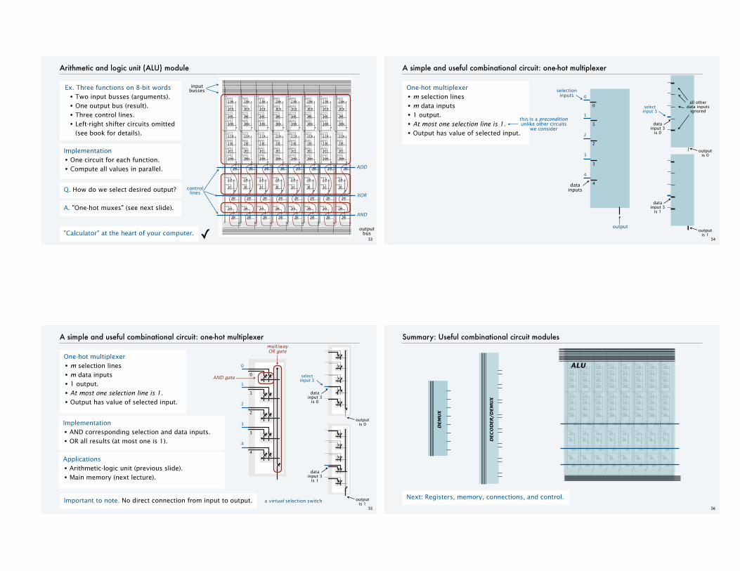
Arithmetic and logic unit (ALU) module
Ex. Three functions on 8-bit words • Two input busses (arguments). • One output bus (result). • Three control lines.
52
output bus
input busses
control lines
ADD
XOR
AND
ALU (8-bit)
Arithmetic and logic unit (ALU) module
Ex. Three functions on 8-bit words • Two input busses (arguments). • One output bus (result). • Three control lines. • Left-right shifter circuits omitted
(see book for details).
53
output bus
input busses
control lines
ADD
XOR
AND
Implementation • One circuit for each function. • Compute all values in parallel.
"Calculator" at the heart of your computer. ✓
Q. How do we select desired output?
A. "One-hot muxes" (see next slide).
A simple and useful combinational circuit: one-hot multiplexer
54
output
0
1
2
3
4
selection inputs
0
1
2
3
4datainputs
select input 3
data input 3
is 0
output is 0
output is 1
data input 3
is 1
One-hot multiplexer • m selection lines • m data inputs • 1 output. • At most one selection line is 1. • Output has value of selected input.
all other data inputs
ignored
this is a precondition unlike other circuits
we consider
55
A simple and useful combinational circuit: one-hot multiplexer
Implementation • AND corresponding selection and data inputs. • OR all results (at most one is 1).
Applications • Arithmetic-logic unit (previous slide). • Main memory (next lecture).
One-hot multiplexer • m selection lines • m data inputs • 1 output. • At most one selection line is 1. • Output has value of selected input.
select input 3
data input 3
is 0
output is 0
output is 1
data input 3
is 1
Important to note. No direct connection from input to output.
0
1
2
3
4
3
0
1
4
2
AND gate
multiway OR gate
a virtual selection switch56
Summary: Useful combinational circuit modules
Next: Registers, memory, connections, and control.
ALU
DEM
UX
DEC
OD
ER
/DEM
UX
C O M P U T E R S C I E N C E S E D G E W I C K / W A Y N E