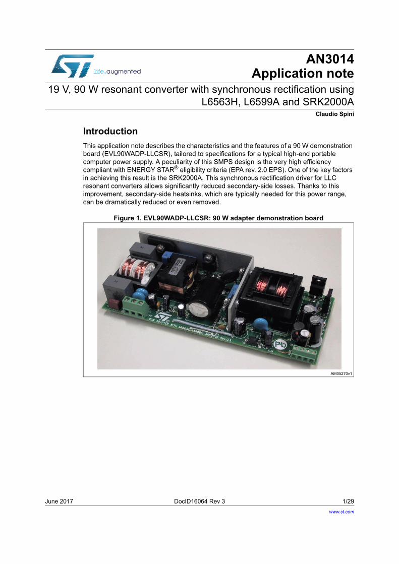
June 2017 DocID16064 Rev 3 1/29 29 AN3014 Application note 19 V, 90 W resonant converter with synchronous rectification using L6563H, L6599A and SRK2000A Claudio Spini Introduction This application note describes the characteristics and the features of a 90 W demonstration board (EVL90WADP-LLCSR), tailored to specifications for a typical high-end portable computer power supply. A peculiarity of this SMPS design is the very high efficiency compliant with ENERGY STAR ® eligibility criteria (EPA rev. 2.0 EPS). One of the key factors in achieving this result is the SRK2000A. This synchronous rectification driver for LLC resonant converters allows significantly reduced secondary-side losses. Thanks to this improvement, secondary-side heatsinks, which are typically needed for this power range, can be dramatically reduced or even removed. Figure 1. EVL90WADP-LLCSR: 90 W adapter demonstration board www.st.com
Transcript
June 2017 DocID16064 Rev 3 1/29
29
AN3014Application note
19 V, 90 W resonant converter with synchronous rectification usingL6563H, L6599A and SRK2000A
Claudio Spini
Introduction
This application note describes the characteristics and the features of a 90 W demonstration board (EVL90WADP-LLCSR), tailored to specifications for a typical high-end portable computer power supply. A peculiarity of this SMPS design is the very high efficiency compliant with ENERGY STAR® eligibility criteria (EPA rev. 2.0 EPS). One of the key factors in achieving this result is the SRK2000A. This synchronous rectification driver for LLC resonant converters allows significantly reduced secondary-side losses. Thanks to this improvement, secondary-side heatsinks, which are typically needed for this power range, can be dramatically reduced or even removed.
Figure 1. EVL90WADP-LLCSR: 90 W adapter demonstration board
Output voltage: 19 V at 4.75 A continuous operation
Mains harmonics: according to EN61000-3-2 class-D or JEITA-MITI class-D
Standby mains consumption: < 0.26 W at 230 Vac
Efficiency at nominal load: > 92% at 115 Vac
EMI: according to EN55022-class-B
Safety: according to EN60950
Dimensions: 65 x 155 mm, 25 mm maximum component height
PCB: double-sided, 70 µm, FR-4, mixed PTH/SMT
The circuit is composed of two stages: a front-end PFC using the L6563H, and a LLC resonant converter based on the L6599A. The SRK2000A controls the synchronous rectification on the secondary side. The PFC stage works as a preregulator and powers the resonant stage with a constant voltage of 400 V. The downstream converter operates only if the PFC is on and regulating. In this way, the resonant stage can be optimized for a narrow input voltage range.
Startup sequence
As indicated previously, the PFC acts as master and the resonant stage can operate only if the PFC output is delivering the nominal output voltage. Therefore the circuit is designed so that at startup the PFC starts first, then the downstream converter turns on. Initially, the L6563H is supplied by the integrated high voltage startup circuit, but as soon as the PFC starts switching, a charge pump connected to the PFC inductor supplies both the PFC and resonant controllers. Once both stages have been activated, the controllers are supplied also by the auxiliary winding of the resonant transformer, assuring correct supply voltage even during standby operation.
Because the L6563H integrated HV startup circuit is turned off and therefore is not dissipative during normal operation, it significantly contributes to the reduction of power consumption when the power supply operates at light load, in accordance with current world-wide standby consumption standards.
Brownout protection
Brownout protection prevents the circuit from working with abnormal mains levels. It is easily achieved using the RUN pin (pin12) of the L6563H. This pin is connected through a resistor divider to the VFF pin (pin 5), which provides the mains voltage peak value information. An internal comparator enables the IC operations if the mains level is correct, within the nominal limits. At startup, if the input voltage is below 90 Vac (typ), circuit operations are inhibited.
The L6599A has similar protection on the LINE pin (pin 7). It is used to prevent the resonant converter from working with too low an input voltage, which can cause incorrect capacitive mode operation. If the bulk voltage (PFC output) is below 380 V, the resonant startup is not allowed. The L6599A internal comparator has a hysteresis which allows the turn-on and turn-off voltage to be set independently. The turn-off threshold has been set to 300 V in
Main characteristics and circuit description AN3014
6/29 DocID16064 Rev 3
order to avoid capacitive mode operation, but to allow the resonant stage to operate even in case of mains sag and consequent PFC output dip.
Fast voltage feed-forward
The voltage on the L6563H VFF pin (pin 5) is the peak value of the voltage on the MULT pin (pin 3). The RC network (R15+R26, C12) connected to VFF completes the peak-holding circuit. This signal is necessary to derive RMS input voltage information to compensate the loop gain, which is mains voltage dependent.
Generally speaking, if the time constant is too small, the voltage generated is affected by a considerable amount of ripple at twice the mains frequency, thus causing distortion of the current reference (resulting in high THD and poor PF). If the time constant is too large, there is a considerable delay in setting the right amount of feed-forward, resulting in excessive overshoot or undershoot of the preregulator's output voltage in response to large line voltage changes.
To overcome this issue, the L6563H implements the new fast voltage feed-forward function. As soon as the voltage on the VFF pin decreases to a set threshold (40 mV typically), a mains dip is assumed and an internal switch rapidly discharges the VFF capacitor via a 10-k resistor. Thanks to this feature, it is possible to set an RC circuit with a long time constant, assuring a low THD and maintaining a fast response to mains dip.
Resonant power stage
The downstream converter employs ST’s L6599A, which incorporates all the functions necessary to properly control the resonant converter with a 50% fixed duty cycle and works with a variable frequency.
The transformer uses the integrated magnetic approach, incorporating a resonant series inductor. Thus, no additional external coil is needed for the resonance. The transformer configuration chosen for the secondary winding is center tap.
On the secondary side, the output rectification is controlled by the SRK2000A, an SR driver dedicated to LLC resonant topology.
A small LC filter has been added on the output, filtering the high-frequency ripple.
D15, R56, R62, R65, R66, Q5 and Q6 implement an output voltage “fast discharge” circuit which quickly discharges the output capacitors when the converter is turned off. It has been implemented to quickly decrease the residual output voltage after the converter is turned off at no load.
Output voltage feedback loop
The feedback loop is implemented by means of a typical circuit using a TL431 to modulate the current in the optocoupler diode.
On the primary side, R34 - connecting the RFMIN pin (pin 4) to the optocoupler phototransistor - closes the feedback loop and its value sets the maximum switching frequency at about 130 kHz. This value has been chosen to limit the switching losses at light load operation. R31, which connects the same pin to ground, sets the minimum switching frequency. The R-C series (R44 and C18) sets both the soft-start maximum frequency and duration.
DocID16064 Rev 3 7/29
AN3014 Main characteristics and circuit description
29
L6599A overload and short-circuit protection
The current into the primary winding is sensed by the lossless circuit R41, C27, D11, D10, R39, and C25 and is fed to the ISEN pin (pin 6). In case of overcurrent, the voltage on the pin passes an internal threshold (0.8 V), triggering a protection sequence. The capacitor (C45) connected to the DELAY pin (pin 2) is charged by an internal 150-µA current generator and is slowly discharged by the external resistor (R24). If the voltage on the pin reaches 2 V, the soft-start capacitor is completely discharged so that the switching frequency is pushed to its maximum value. As the voltage on the pin exceeds 3.5 V, the IC stops switching and the internal generator is turned off, so that the voltage on the pin decays due to the external resistor. The IC is soft-restarted as the voltage drops below 0.3 V. In this way, under short-circuit conditions, the converter works intermittently with very low input average power.
Overvoltage and open loop protection
Both the PFC and resonant circuit stages are equipped with their own overvoltage protection.
The PFC controller L6563H monitors its output voltage via the resistor divider connected to a dedicated pin (PFC_OK, pin 7), protecting the circuit in case of loop failures, disconnection or deviation from the nominal value of the feedback loop divider. If the voltage on pin #7 exceeds 2.5 V the IC stops switching and restarts as the voltage on the pin falls below 2.4 V, preventing the output voltage becoming excessive in case of transient due to the slow response of the error amplifier. However, if contemporaneously the voltage of the INV pin falls below 1.66 V (typ.), a feedback failure is assumed. In this case the PFC_OK circuitry latches the L6563H operations and, by means of the PWM_LATCH pin (pin 8) it latches the L6599A as well, via the DIS pin (pin 8). The converter is kept latched by the L6563H HV circuit which supplies the IC, charging the VCC capacitor periodically. To resume converter operation, mains restart is necessary.
The DIS pin is used to protect also the resonant stage against overvoltage. The Zener diode D8 detects the auxiliary voltage, which is proportional to the output voltage. In case of loop failure it conducts and voltage on the DIS pin exceeds the internal threshold, and latches off the device. L6563H operation is also stopped by the PFC_STOP pin.
Secondary-side synchronous rectification with the SRK2000A
The SRK2000A core function is to switch on each synchronous rectifier MOSFET whenever the corresponding transformer half-winding starts conducting (i.e. when the MOSFET body diode starts conducting), and then to switch it off when the current flowing through it approaches zero. For this purpose, the IC is equipped with two pins (DVS1 and DVS2) capable of sensing the MOSFET drain voltage level.
Standby power saving
The board has a burst-mode function implemented, allowing power saving during light load operation.
The L6599A STBY pin (pin 5) senses the optocoupler’s collector voltage, which is related to the feedback control. This signal is compared to an internal reference (1.24 V). If the voltage on the pin is lower than the reference, the IC enters an idle state and its quiescent current is reduced. As the voltage exceeds the reference by 50 mV, the controller restarts the switching. The burst-mode operation load threshold can be programmed by properly choosing the resistor connecting the optocoupler to the RFMIN pin (R34). On this board, the controller operates in burst-mode if the load falls below ~10 W.
Main characteristics and circuit description AN3014
8/29 DocID16064 Rev 3
The L6563H implements its own burst-mode function. If the COMP voltage falls below 2.5 V, the IC stops switching, causing an output voltage drop. As a consequence, the COMP voltage rise again and the IC starts switching again.
In order to achieve better load transient response, the PFC burst-mode operation is partially forced by the resonant converter: as soon as the L6599A stops switching due to load drops, its PFC_STOP pin pulls down the L6563H's PFC_OK pin, disabling PFC switching. Thanks to this simple circuit, the PFC is forced into an idle state when the resonant stage is not switching, and rapidly wakes up when the downstream converter restarts switching. This solution prevents significant drop of the bulk voltage in case of abrupt load rising.
DocID16064 Rev 3 9/29
AN3014 Main characteristics and circuit description
29
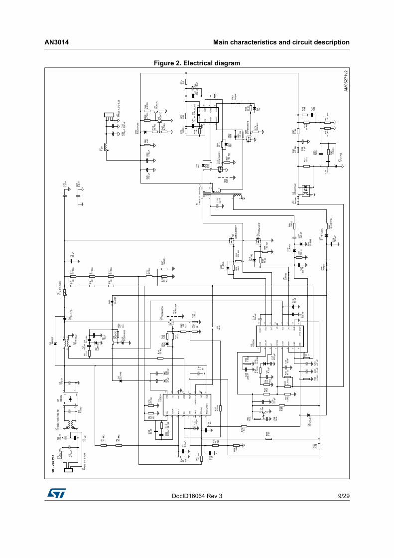
Figure 2. Electrical diagram
Efficiency measurement AN3014
10/29 DocID16064 Rev 3
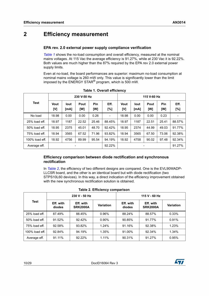
2 Efficiency measurement
EPA rev. 2.0 external power supply compliance verification
Table 1 shows the no-load consumption and overall efficiency, measured at the nominal mains voltages. At 115 Vac the average efficiency is 91.27%, while at 230 Vac it is 92.22%. Both values are much higher than the 87% required by the EPA rev 2.0 external power supply limits.
Even at no-load, the board performances are superior: maximum no-load consumption at nominal mains voltage is 260 mW only. This value is significantly lower than the limit imposed by the ENERGY STAR® program, which is 500 mW.
Efficiency comparison between diode rectification and synchronous rectification
In Table 2, the efficiency of two different designs are compared. One is the EVL90WADP-LLCSR board, and the other is an identical board but with diode rectification (two STPS10L60 devices). In this way, a direct indication of the efficiency improvement obtained with the new synchronous rectification solution is obtained.
Average eff. 91.11% 92.22% 1.11% 90.31% 91.27% 0.95%
DocID16064 Rev 3 11/29
AN3014 Efficiency measurement
29
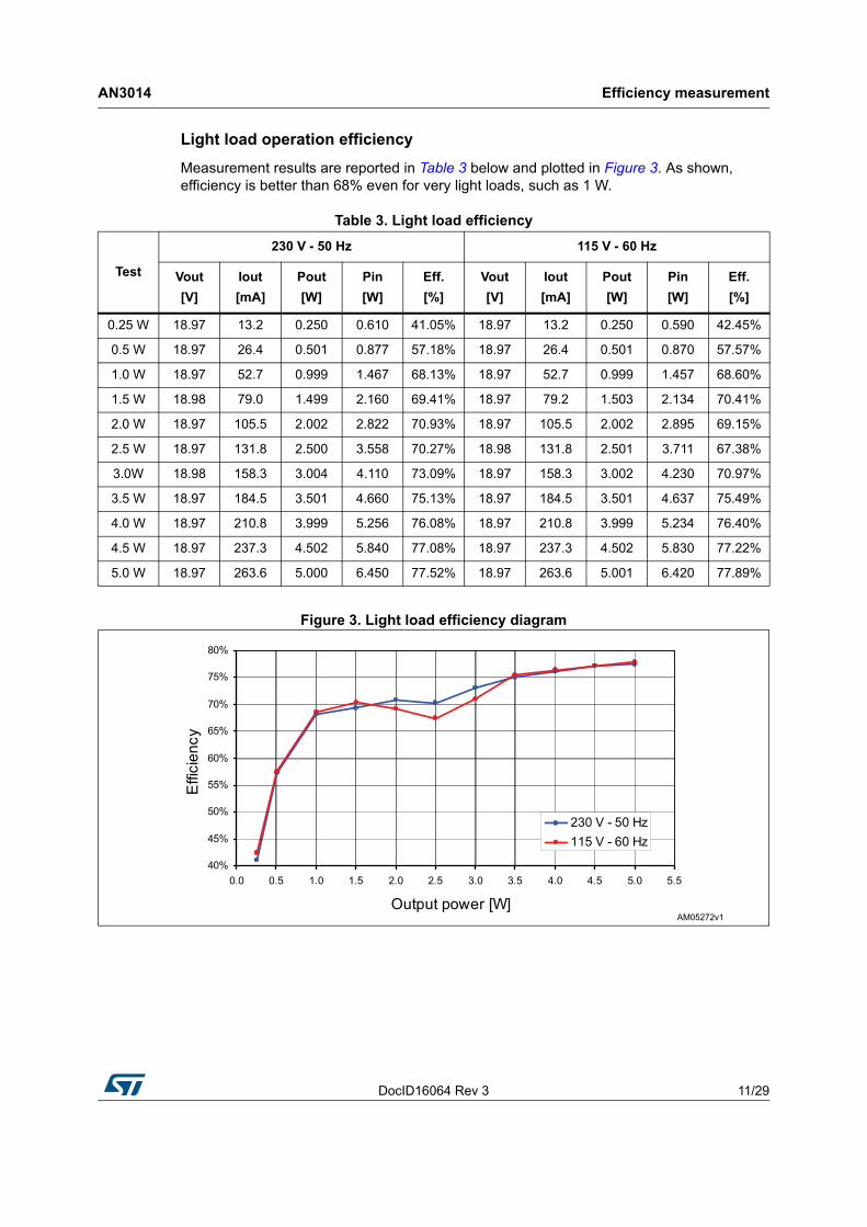
Light load operation efficiency
Measurement results are reported in Table 3 below and plotted in Figure 3. As shown, efficiency is better than 68% even for very light loads, such as 1 W.
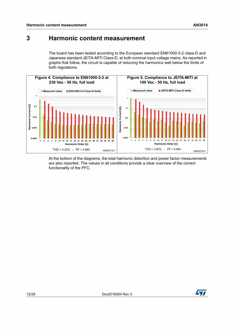
The board has been tested according to the European standard EN61000-3-2 class-D and Japanese standard JEITA-MITI Class-D, at both nominal input voltage mains. As reported in graphs that follow, the circuit is capable of reducing the harmonics well below the limits of both regulations.
At the bottom of the diagrams, the total harmonic distortion and power factor measurements are also reported. The values in all conditions provide a clear overview of the correct functionality of the PFC.
Figure 4. Compliance to EN61000-3-2 at230 Vac - 50 Hz, full load
Figure 5. Compliance to JEITA-MITI at100 Vac - 50 Hz, full load
DocID16064 Rev 3 13/29
AN3014 Functional check
29
4 Functional check
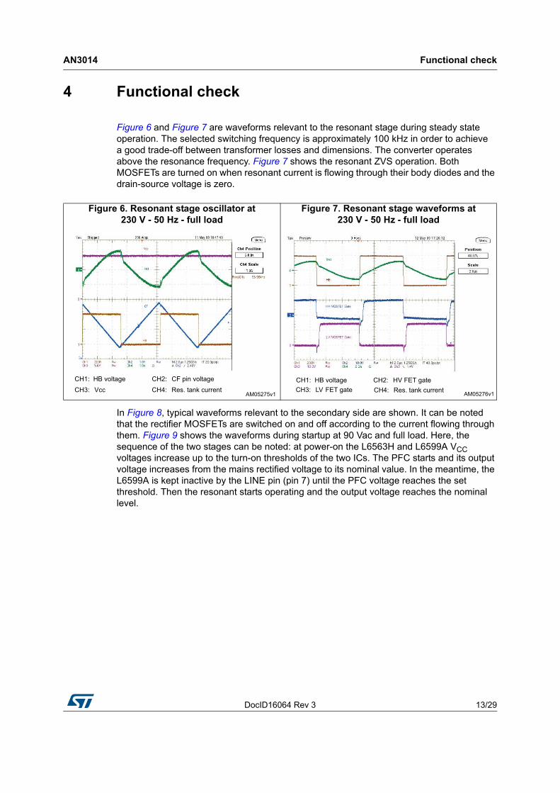
Figure 6 and Figure 7 are waveforms relevant to the resonant stage during steady state operation. The selected switching frequency is approximately 100 kHz in order to achieve a good trade-off between transformer losses and dimensions. The converter operates above the resonance frequency. Figure 7 shows the resonant ZVS operation. Both MOSFETs are turned on when resonant current is flowing through their body diodes and the drain-source voltage is zero.
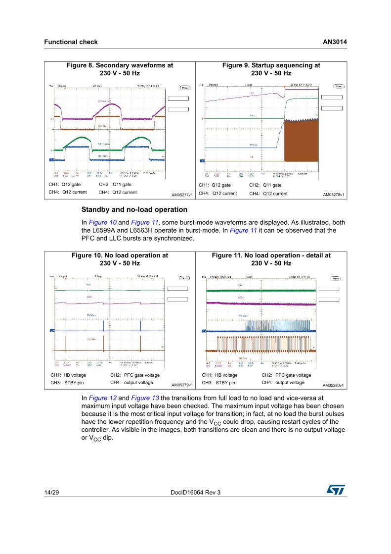
In Figure 8, typical waveforms relevant to the secondary side are shown. It can be noted that the rectifier MOSFETs are switched on and off according to the current flowing through them. Figure 9 shows the waveforms during startup at 90 Vac and full load. Here, the sequence of the two stages can be noted: at power-on the L6563H and L6599A VCC voltages increase up to the turn-on thresholds of the two ICs. The PFC starts and its output voltage increases from the mains rectified voltage to its nominal value. In the meantime, the L6599A is kept inactive by the LINE pin (pin 7) until the PFC voltage reaches the set threshold. Then the resonant starts operating and the output voltage reaches the nominal level.
Figure 6. Resonant stage oscillator at230 V - 50 Hz - full load
Figure 7. Resonant stage waveforms at230 V - 50 Hz - full load
Functional check AN3014
14/29 DocID16064 Rev 3
Standby and no-load operation
In Figure 10 and Figure 11, some burst-mode waveforms are displayed. As illustrated, both the L6599A and L6563H operate in burst-mode. In Figure 11 it can be observed that the PFC and LLC bursts are synchronized.
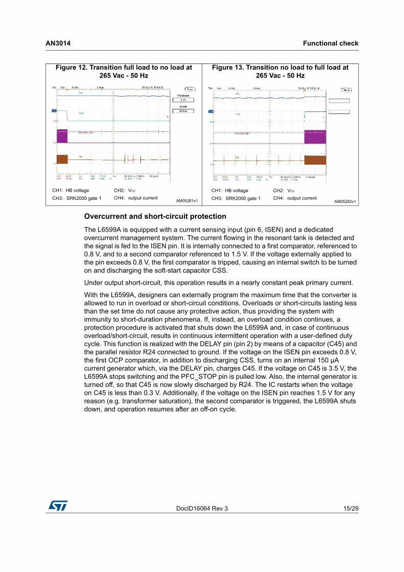
In Figure 12 and Figure 13 the transitions from full load to no load and vice-versa at maximum input voltage have been checked. The maximum input voltage has been chosen because it is the most critical input voltage for transition; in fact, at no load the burst pulses have the lower repetition frequency and the VCC could drop, causing restart cycles of the controller. As visible in the images, both transitions are clean and there is no output voltage or VCC dip.
Figure 8. Secondary waveforms at230 V - 50 Hz
Figure 9. Startup sequencing at230 V - 50 Hz
Figure 10. No load operation at230 V - 50 Hz
Figure 11. No load operation - detail at230 V - 50 Hz
DocID16064 Rev 3 15/29
AN3014 Functional check
29
Overcurrent and short-circuit protection
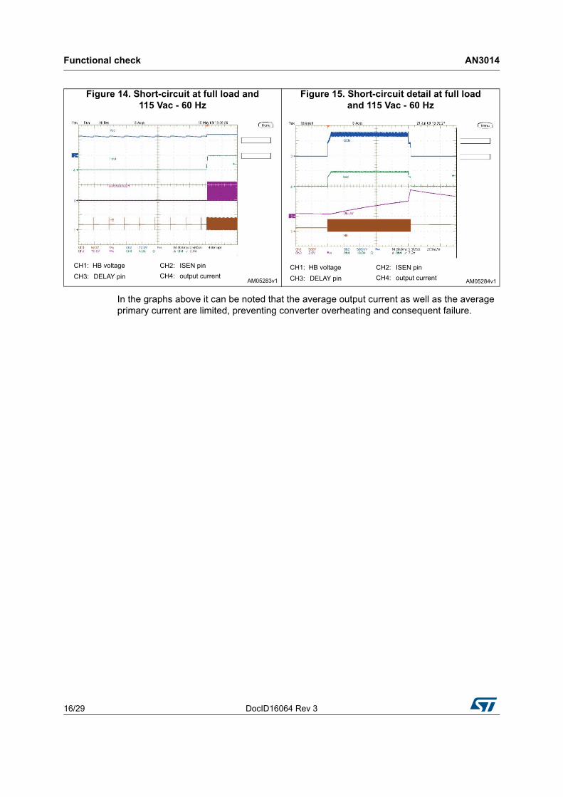
The L6599A is equipped with a current sensing input (pin 6, ISEN) and a dedicated overcurrent management system. The current flowing in the resonant tank is detected and the signal is fed to the ISEN pin. It is internally connected to a first comparator, referenced to 0.8 V, and to a second comparator referenced to 1.5 V. If the voltage externally applied to the pin exceeds 0.8 V, the first comparator is tripped, causing an internal switch to be turned on and discharging the soft-start capacitor CSS.
Under output short-circuit, this operation results in a nearly constant peak primary current.
With the L6599A, designers can externally program the maximum time that the converter is allowed to run in overload or short-circuit conditions. Overloads or short-circuits lasting less than the set time do not cause any protective action, thus providing the system with immunity to short-duration phenomena. If, instead, an overload condition continues, a protection procedure is activated that shuts down the L6599A and, in case of continuous overload/short-circuit, results in continuous intermittent operation with a user-defined duty cycle. This function is realized with the DELAY pin (pin 2) by means of a capacitor (C45) and the parallel resistor R24 connected to ground. If the voltage on the ISEN pin exceeds 0.8 V, the first OCP comparator, in addition to discharging CSS, turns on an internal 150 µA current generator which, via the DELAY pin, charges C45. If the voltage on C45 is 3.5 V, the L6599A stops switching and the PFC_STOP pin is pulled low. Also, the internal generator is turned off, so that C45 is now slowly discharged by R24. The IC restarts when the voltage on C45 is less than 0.3 V. Additionally, if the voltage on the ISEN pin reaches 1.5 V for any reason (e.g. transformer saturation), the second comparator is triggered, the L6599A shuts down, and operation resumes after an off-on cycle.
Figure 12. Transition full load to no load at265 Vac - 50 Hz
Figure 13. Transition no load to full load at265 Vac - 50 Hz
Functional check AN3014
16/29 DocID16064 Rev 3
In the graphs above it can be noted that the average output current as well as the average primary current are limited, preventing converter overheating and consequent failure.
Figure 14. Short-circuit at full load and115 Vac - 60 Hz
Figure 15. Short-circuit detail at full loadand 115 Vac - 60 Hz
DocID16064 Rev 3 17/29
AN3014 Thermal map
29
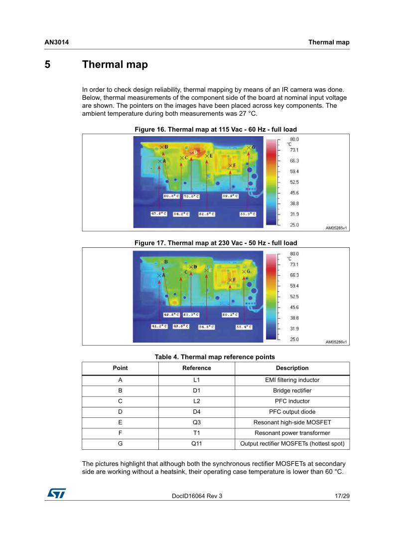
5 Thermal map
In order to check design reliability, thermal mapping by means of an IR camera was done. Below, thermal measurements of the component side of the board at nominal input voltage are shown. The pointers on the images have been placed across key components. The ambient temperature during both measurements was 27 °C.
Figure 16. Thermal map at 115 Vac - 60 Hz - full load
Figure 17. Thermal map at 230 Vac - 50 Hz - full load
The pictures highlight that although both the synchronous rectifier MOSFETs at secondary side are working without a heatsink, their operating case temperature is lower than 60 °C.
Table 4. Thermal map reference points
Point Reference Description
A L1 EMI filtering inductor
B D1 Bridge rectifier
C L2 PFC inductor
D D4 PFC output diode
E Q3 Resonant high-side MOSFET
F T1 Resonant power transformer
G Q11 Output rectifier MOSFETs (hottest spot)
Conducted emission pre-compliance test AN3014
18/29 DocID16064 Rev 3
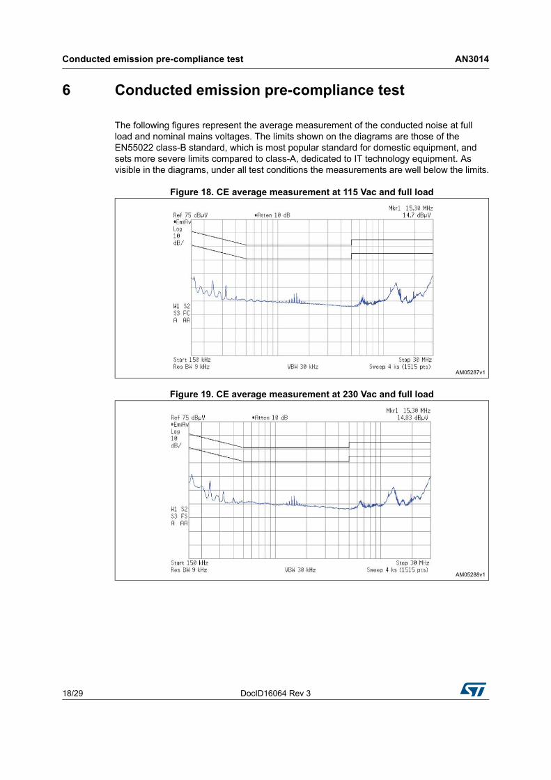
6 Conducted emission pre-compliance test
The following figures represent the average measurement of the conducted noise at full load and nominal mains voltages. The limits shown on the diagrams are those of the EN55022 class-B standard, which is most popular standard for domestic equipment, and sets more severe limits compared to class-A, dedicated to IT technology equipment. As visible in the diagrams, under all test conditions the measurements are well below the limits.
Figure 18. CE average measurement at 115 Vac and full load
Figure 19. CE average measurement at 230 Vac and full load
DocID16064 Rev 3 19/29
AN3014 Bill of material
29
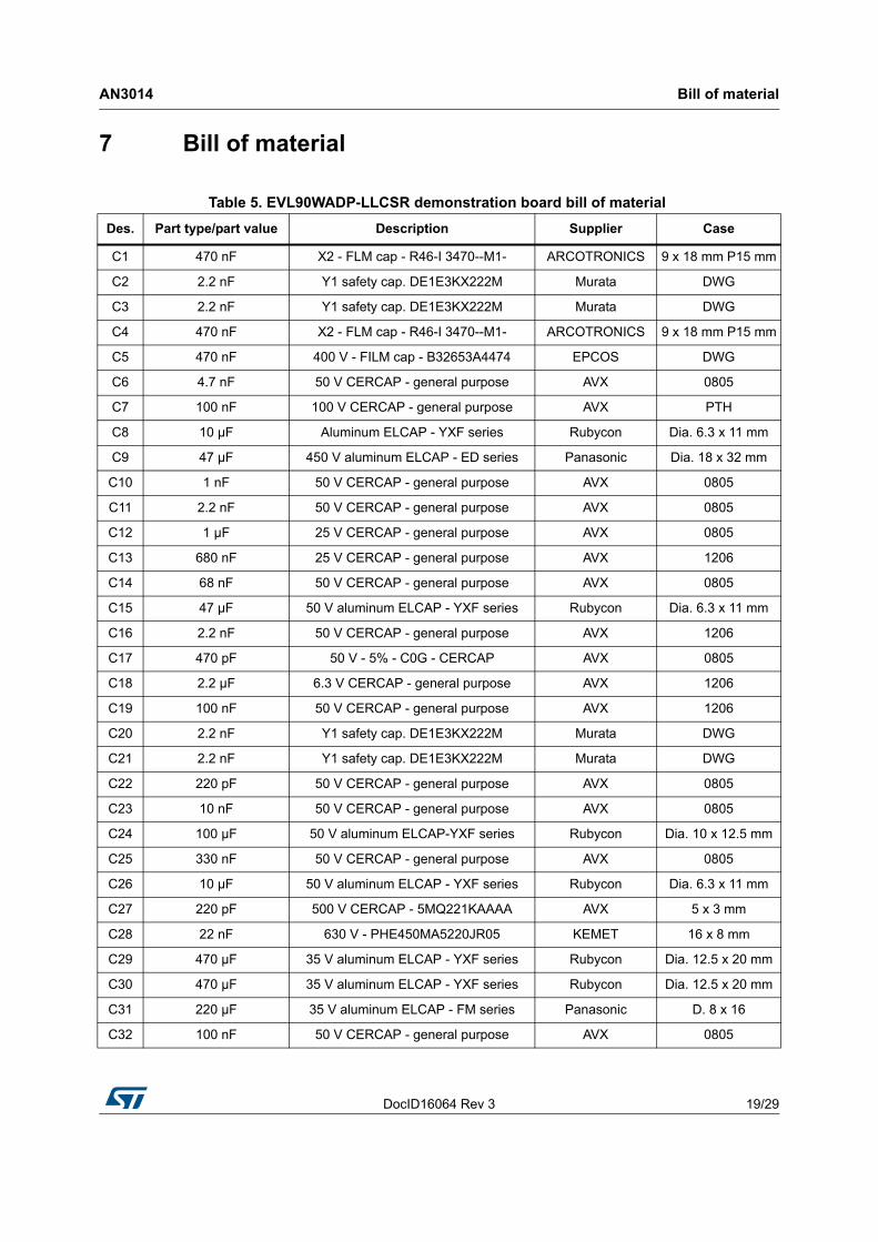
7 Bill of material
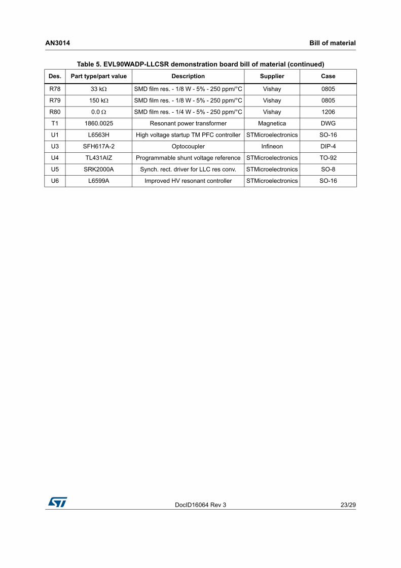
Table 5. EVL90WADP-LLCSR demonstration board bill of material
Des. Part type/part value Description Supplier Case
C1 470 nF X2 - FLM cap - R46-I 3470--M1- ARCOTRONICS 9 x 18 mm P15 mm
C2 2.2 nF Y1 safety cap. DE1E3KX222M Murata DWG
C3 2.2 nF Y1 safety cap. DE1E3KX222M Murata DWG
C4 470 nF X2 - FLM cap - R46-I 3470--M1- ARCOTRONICS 9 x 18 mm P15 mm
C5 470 nF 400 V - FILM cap - B32653A4474 EPCOS DWG
C6 4.7 nF 50 V CERCAP - general purpose AVX 0805
C7 100 nF 100 V CERCAP - general purpose AVX PTH
C8 10 µF Aluminum ELCAP - YXF series Rubycon Dia. 6.3 x 11 mm
C9 47 µF 450 V aluminum ELCAP - ED series Panasonic Dia. 18 x 32 mm
C10 1 nF 50 V CERCAP - general purpose AVX 0805
C11 2.2 nF 50 V CERCAP - general purpose AVX 0805
C12 1 µF 25 V CERCAP - general purpose AVX 0805
C13 680 nF 25 V CERCAP - general purpose AVX 1206
C14 68 nF 50 V CERCAP - general purpose AVX 0805
C15 47 µF 50 V aluminum ELCAP - YXF series Rubycon Dia. 6.3 x 11 mm
C16 2.2 nF 50 V CERCAP - general purpose AVX 1206
C17 470 pF 50 V - 5% - C0G - CERCAP AVX 0805
C18 2.2 µF 6.3 V CERCAP - general purpose AVX 1206
C19 100 nF 50 V CERCAP - general purpose AVX 1206
C20 2.2 nF Y1 safety cap. DE1E3KX222M Murata DWG
C21 2.2 nF Y1 safety cap. DE1E3KX222M Murata DWG
C22 220 pF 50 V CERCAP - general purpose AVX 0805
C23 10 nF 50 V CERCAP - general purpose AVX 0805
C24 100 µF 50 V aluminum ELCAP-YXF series Rubycon Dia. 10 x 12.5 mm
C25 330 nF 50 V CERCAP - general purpose AVX 0805
C26 10 µF 50 V aluminum ELCAP - YXF series Rubycon Dia. 6.3 x 11 mm
C27 220 pF 500 V CERCAP - 5MQ221KAAAA AVX 5 x 3 mm
C28 22 nF 630 V - PHE450MA5220JR05 KEMET 16 x 8 mm
C29 470 µF 35 V aluminum ELCAP - YXF series Rubycon Dia. 12.5 x 20 mm
C30 470 µF 35 V aluminum ELCAP - YXF series Rubycon Dia. 12.5 x 20 mm
C31 220 µF 35 V aluminum ELCAP - FM series Panasonic D. 8 x 16
C32 100 nF 50 V CERCAP - general purpose AVX 0805
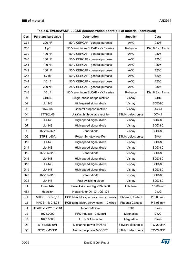
Bill of material AN3014
20/29 DocID16064 Rev 3
C34 220 nF 50 V CERCAP - general purpose AVX 0805
C36 1 µF 50 V aluminum ELCAP - YXF series Rubycon Dia. 6.3 x 11 mm
C39 100 nF 50 V CERCAP - general purpose AVX 0805
C40 100 nF 50 V CERCAP - general purpose AVX 1206
C41 100 nF 50 V CERCAP - general purpose AVX 0805
C42 100 nF 50 V CERCAP - general purpose AVX 1206
C43 4.7 nF 50 V CERCAP - general purpose AVX 1206
C44 10 nF 50 V CERCAP - general purpose AVX 1206
C45 220 nF 25 V CERCAP - general purpose AVX 0805
C48 10 µF 50 V aluminum ELCAP - YXF series Rubycon Dia. 6.3 x 11 mm
Table 5. EVL90WADP-LLCSR demonstration board bill of material (continued)
Des. Part type/part value Description Supplier Case
PFC coil specification AN3014
24/29 DocID16064 Rev 3
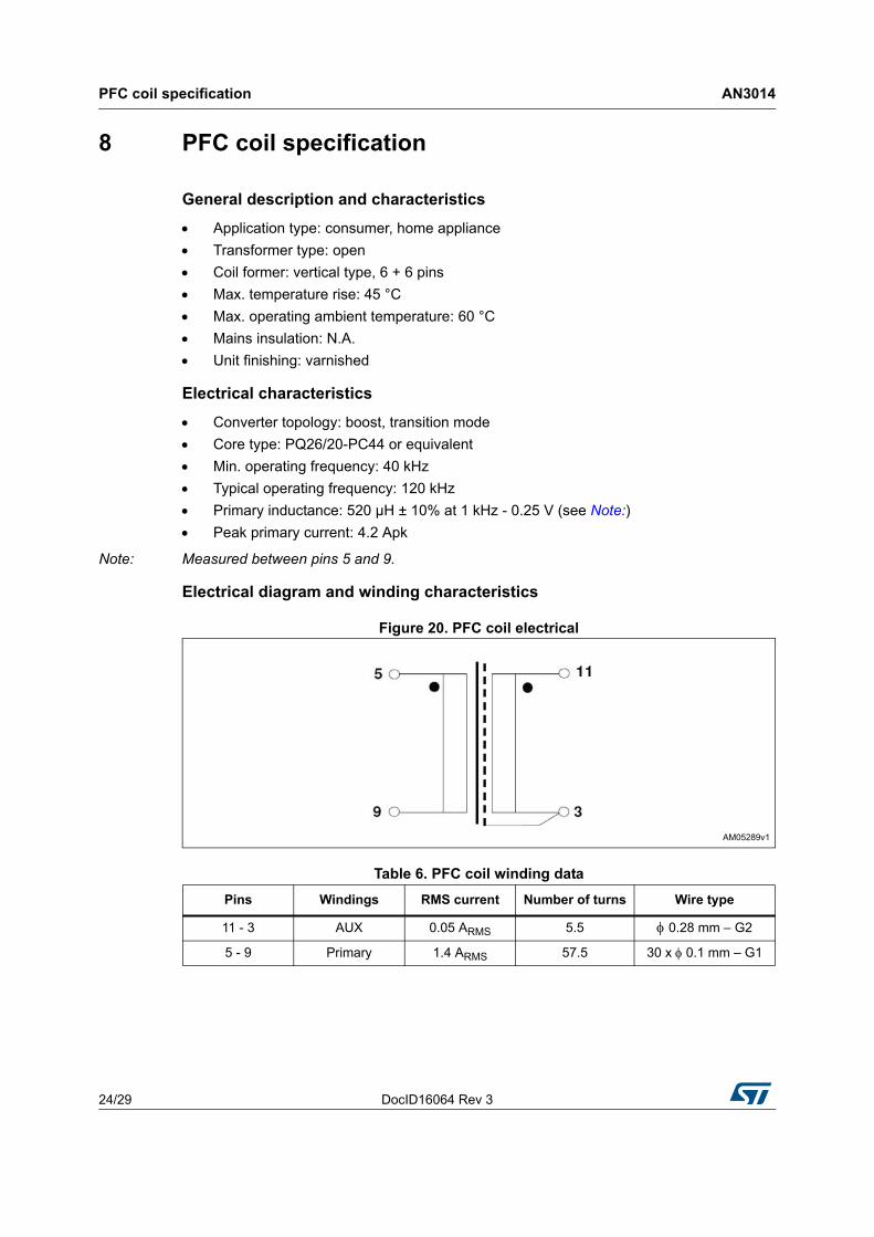
8 PFC coil specification
General description and characteristics
Application type: consumer, home appliance
Transformer type: open
Coil former: vertical type, 6 + 6 pins
Max. temperature rise: 45 °C
Max. operating ambient temperature: 60 °C
Mains insulation: N.A.
Unit finishing: varnished
Electrical characteristics
Converter topology: boost, transition mode
Core type: PQ26/20-PC44 or equivalent
Min. operating frequency: 40 kHz
Typical operating frequency: 120 kHz
Primary inductance: 520 µH ± 10% at 1 kHz - 0.25 V (see Note:)
Peak primary current: 4.2 Apk
Note: Measured between pins 5 and 9.
Electrical diagram and winding characteristics
Figure 20. PFC coil electrical
Table 6. PFC coil winding data
Pins Windings RMS current Number of turns Wire type
11 - 3 AUX 0.05 ARMS 5.5 0.28 mm – G2
5 - 9 Primary 1.4 ARMS 57.5 30 x 0.1 mm – G1
DocID16064 Rev 3 25/29
AN3014 PFC coil specification
29
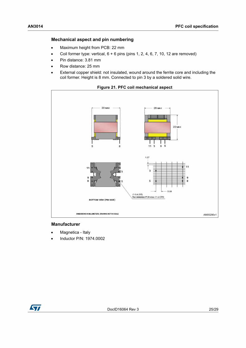
Mechanical aspect and pin numbering
Maximum height from PCB: 22 mm
Coil former type: vertical, 6 + 6 pins (pins 1, 2, 4, 6, 7, 10, 12 are removed)
Pin distance: 3.81 mm
Row distance: 25 mm
External copper shield: not insulated, wound around the ferrite core and including the coil former. Height is 8 mm. Connected to pin 3 by a soldered solid wire.
Figure 21. PFC coil mechanical aspect
Manufacturer
Magnetica - Italy
Inductor P/N: 1974.0002
Transformer specification AN3014
26/29 DocID16064 Rev 3
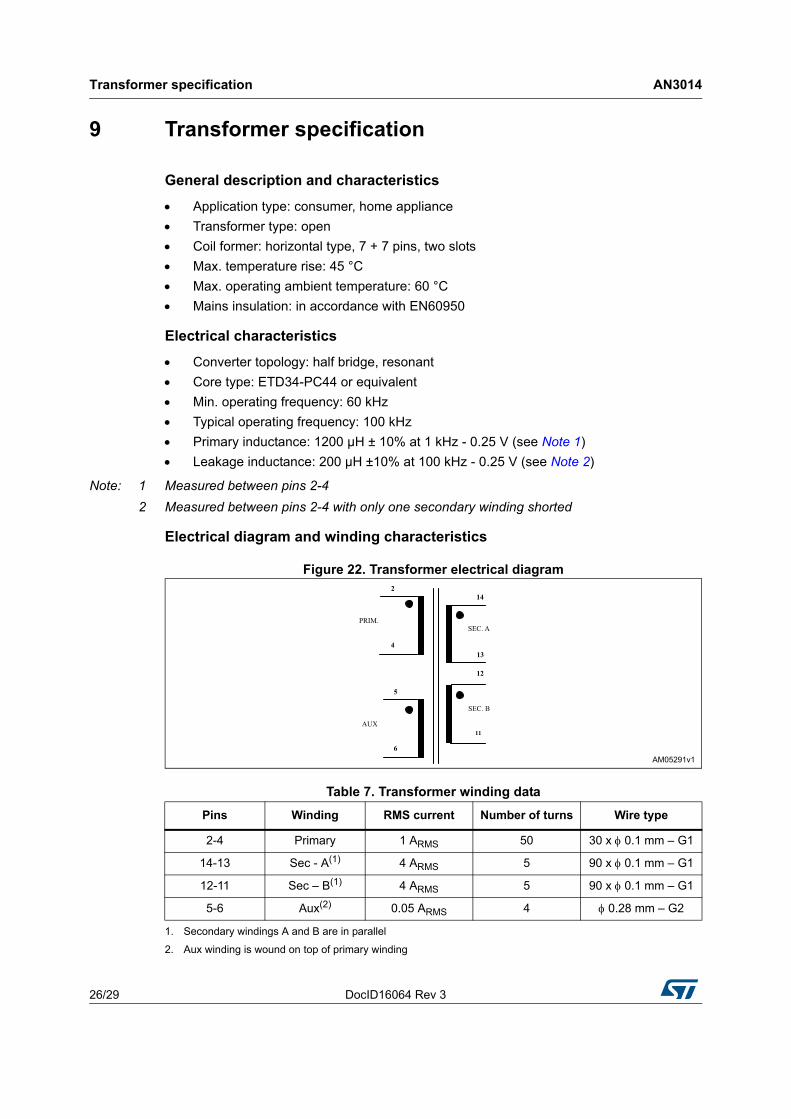
9 Transformer specification
General description and characteristics
Application type: consumer, home appliance
Transformer type: open
Coil former: horizontal type, 7 + 7 pins, two slots
Max. temperature rise: 45 °C
Max. operating ambient temperature: 60 °C
Mains insulation: in accordance with EN60950
Electrical characteristics
Converter topology: half bridge, resonant
Core type: ETD34-PC44 or equivalent
Min. operating frequency: 60 kHz
Typical operating frequency: 100 kHz
Primary inductance: 1200 µH ± 10% at 1 kHz - 0.25 V (see Note 1)
Leakage inductance: 200 µH ±10% at 100 kHz - 0.25 V (see Note 2)
Note: 1 Measured between pins 2-4
2 Measured between pins 2-4 with only one secondary winding shorted
Electrical diagram and winding characteristics
Figure 22. Transformer electrical diagram
Table 7. Transformer winding data
Pins Winding RMS current Number of turns Wire type
2-4 Primary 1 ARMS 50 30 x 0.1 mm – G1
14-13 Sec - A(1)
1. Secondary windings A and B are in parallel
4 ARMS 5 90 x 0.1 mm – G1
12-11 Sec – B(1) 4 ARMS 5 90 x 0.1 mm – G1
5-6 Aux(2)
2. Aux winding is wound on top of primary winding
0.05 ARMS 4 0.28 mm – G2
DocID16064 Rev 3 27/29
AN3014 Transformer specification
29
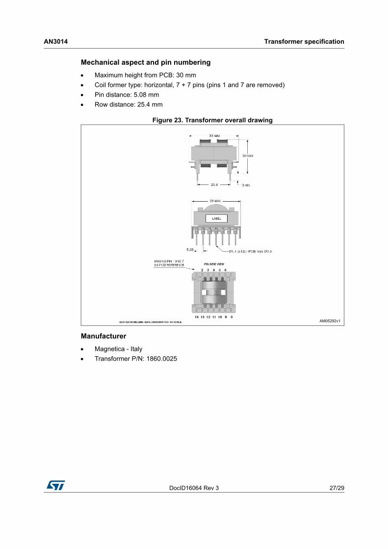
Mechanical aspect and pin numbering
Maximum height from PCB: 30 mm
Coil former type: horizontal, 7 + 7 pins (pins 1 and 7 are removed)
Pin distance: 5.08 mm
Row distance: 25.4 mm
Figure 23. Transformer overall drawing
Manufacturer
Magnetica - Italy
Transformer P/N: 1860.0025
Revision history AN3014
28/29 DocID16064 Rev 3
10 Revision history
Table 8. Document revision history
Date Revision Changes
22-Mar-2010 1 Initial release.
13-Dec-2010 2 Updated Chapter 1
14-Jun-2017 3
Replaced “SRK2000” by “SRK2000A” in the whole document.
Replaced Figure 2 on page 9 by new figure.
Minor modifications throughout document.
DocID16064 Rev 3 29/29
AN3014
29
IMPORTANT NOTICE – PLEASE READ CAREFULLY
STMicroelectronics NV and its subsidiaries (“ST”) reserve the right to make changes, corrections, enhancements, modifications, and improvements to ST products and/or to this document at any time without notice. Purchasers should obtain the latest relevant information on ST products before placing orders. ST products are sold pursuant to ST’s terms and conditions of sale in place at the time of order acknowledgement.
Purchasers are solely responsible for the choice, selection, and use of ST products and ST assumes no liability for application assistance or the design of Purchasers’ products.
No license, express or implied, to any intellectual property right is granted by ST herein.
Resale of ST products with provisions different from the information set forth herein shall void any warranty granted by ST for such product.
ST and the ST logo are trademarks of ST. All other product or service names are the property of their respective owners.
Information in this document supersedes and replaces information previously supplied in any prior versions of this document.