Noise Modeling for Semiconductors -1- modeling toolkits NOISE.DOC | 22.04.02 Franz Sischka 1/f Noise Modeling for Semiconductors NOTE: This docu describes the 1/f bipolar and MOS transistor toolkit before its implementation into IC-CAP as Agilent product number 85195B. 1. Introduction 2. Types of Noise in Semiconductors 3. Noise Models in Semiconductors 4. 1/f Noise Measurement Setup 5. AF, KF and BF/EF Noise Parameter Extraction and Verification 6. Appendix: Noise floor information on the toolkit measurement setup 7. Acknowledgements and Publications F.Sischka Agilent Technologies GmbH, Munich
Transcript
Noise Modeling for Semiconductors -1-
modeling toolkits NOISE.DOC | 22.04.02 Franz Sischka
1/f Noise Modeling for Semiconductors
NOTE:This docu describes the 1/f bipolar and MOS transistor toolkit before its implementation into IC-CAP as Agilentproduct number 85195B.
1. Introduction
2. Types of Noise in Semiconductors
3. Noise Models in Semiconductors
4. 1/f Noise Measurement Setup
5. AF, KF and BF/EF Noise Parameter Extraction and Verification
6. Appendix: Noise floor information on the toolkit measurement setup
7. Acknowledgements and Publications
F.SischkaAgilent Technologies GmbH, Munich
Noise Modeling for Semiconductors -2-
modeling toolkits NOISE.DOC | 22.04.02 Franz Sischka
1. IntroductionPhase noise of oscillator circuits is among the key parameters of today's communicationsystems. It limits the modulation quality of the information signal, and the cross-talk toadjacent channels. In the receiver, on the other hand, it can reduce the selectivity and thedemodulation quality. With today's trend to even more complex modulation schemes, lowphase noise becomes even more critical. Therefore, minimizing noise with the design of highfrequency communications circuits is a must for the cost-effective exploitation of limitedbandwidth, and to obtain low bit error rates.
In order to predict the noise behavior of such systems correctly, accurate noise models arerequired. Without them, the design and optimization of an amplifier's noise figure or the phasenoise of oscillators cannot be successful.
A key element is the transistor. While for linear circuits the modeling of the noise at theoperating frequency f0 is sufficient, non-linear circuits do also convert the low-frequencynoise up to the operating frequency range. For oscillators as an example, the 1/f lowfrequency noise at fm will be mixed upwards to contribute to the phase noise of the totalcircuit at the frequencies f0+fm and f0-fm . Therefore, noise modeling of transistors can besplit into a high and a low frequency segment. Fig.1 depicts the Collector low-frequency noisespectral density [A2/Hz] of a bipolar transistor.It can be seen that the resolution of the toolkit measurement setup is at about Hz/nA2.0 .
Fig.1: low frequency noise spectral density current of a bipolar transistor [A2/Hz], measuredat the Collector.
Broadband noise in bipolar or FET models is determined essentially by thermal noise and shotnoise. These noise sources are automatically determined within the model from the largesignal model parameters. An important prerequisite for this is, however, that the noisedetermining parameters, e.g. the Base resistor of bipolar transistors, has been determinedcarefully and that their values have a physical meaning. The low frequency noise, on the otherhand, dominated by the 1/f noise, is modeled by some specific model parameters. In general,these are the AF and KF and sometimes BF/EF parameters, covered in this chapter. Withsome models, like the BSIM3v3, an alternate 1/f noise model is available too [10,15].
Noise Modeling for Semiconductors -3-
modeling toolkits NOISE.DOC | 22.04.02 Franz Sischka
Since there is much confusion about noise terms, noise units etc., we will first commence witha small chapter on
Noise Terms Definitions
In order to keeps things simple, we consider white noise of a resistor. This frequency-independent and bias-independent noise is described in terms of a voltage by the well-knownformula
RfTk4v 2nR ∗∆⋅⋅⋅=
with
2nRv effective noise voltage (root means square value), in [V2]
fTk4 ∆⋅⋅⋅ this product represents a power, with dimension [A*V]R resistance value
Since the term 4kT∆f represents a power, and if we normalize this power to ∆f, we end upwith a power density. Usually, this normalization is done for ∆f=1Hz .
RTk4f
v 2nR ∗⋅⋅=∆
This result can be plotted against frequency. In case of our resistor, it is a constant value. Forsemiconductors, such a plot can also exhibit frequency dependencies, e.g. 1/f noise. In anycase, such a plot shows a spectrum.
Therefore, this term f
v 2nR∆
is called power noise spectral density.
However, this is not exact, referring to the dimensions. A more appropriate term is thereforevoltage noise spectral density. Its symbol is usually Snv, and its dimension is [V2
/ Hz]
RTk4f
vS2
nRnv ∗⋅⋅=
∆=
In some cases, the square root of Snv is used, called the equivalent noise voltage, Env [V/√Hz].
fvE
2nR
nv ∆=
Note: using Env instead of Snv does not require to calculate noise transmissions/amplificationsusing squares of R, amplification etc. See below.
Noise Modeling for Semiconductors -4-
modeling toolkits NOISE.DOC | 22.04.02 Franz Sischka
Note: When expressing noise in terms of currents, e.g. R1Tk4
fiS
2nR
ni ∗⋅⋅=∆
= , the
same terminology applies.
Note: when performing circuit calculations based on noise spectral densities, keep in mindthat you have to calculate with squares instead of the commonly used expressions!
Sv1 ampl Sv2 = Sv1*(ampl)2
Sv = Si * R2R
SiC = ß2 * SiB
Noise Modeling for Semiconductors -5-
modeling toolkits NOISE.DOC | 22.04.02 Franz Sischka
2. Types of Noise in SemiconductorsThis chapter deals with the description of the different noise mechanisms and their noisedensity spectrum in semiconductor components. It is basically aimed to highlight the mainfundamentals rather than to explain the individual physical effects. We start with the thermalnoise of the ohmic parasitics, and lead then over to the semiconductor-specific noise sources.
Thermal NoiseRelated to the thermal oscillation of electrons in a resistor, we can measure a current at itscontacts, without applying an external voltage. This is the thermal noise current. The effectivecurrent is described by
fR1Tk4i 2
nR ∆⋅⋅⋅⋅= (1)
An equivalent schematic for this condition is a noise-free resistor with a current noise sourcein parallel.
In analogy to this circuit, a noise-free resistor and a serial noise voltage source can be used aswell. In this case, the effective voltage is given by
fRTk4R*iv)1(
22nR
2nR ∆⋅⋅⋅⋅== (2)
See fig. 2.
Fig. 2: equivalent schematic of a noisy resistor
Note: since noise sources have a mean value of '0', but an effective value of usually non-zero,effective voltages and currents are used to calculate the circuit performance with respect tothe noise sources. This means that such an effective voltage is amplified by the square of theamplifier's gain! As another example, two parallel current noise sources can be represented bya single noise current source with a value of
fR1
R1Tk4iii
21
)1(2
2nR2
1nR2
total_nR ∆⋅
+⋅⋅⋅=+=
Also, the ohmic law is now referring to the square of voltages and currents, see equation (2).
Back to the thermal resistor noise, the equivalent noise power density spectra are
( )R1Tk4fCi ⋅⋅⋅= (3)
and ( ) RTk4fCv ⋅⋅⋅= (4)
Noise Modeling for Semiconductors -6-
modeling toolkits NOISE.DOC | 22.04.02 Franz Sischka
These frequency independent noise spectra represent a simplification. An accurate calculationbased on a quantum mechanic model gives
( )
−
+⋅⋅⋅=⋅⋅
1e
121fh
R14fC
Tkfhi (5)
so that equations (1) to (4) are basically only valid for h*f<<k*T , i.e. for ‘low’ frequenciesand high temperatures. However, the quantum noise for h*f>>k*T has to be consideredbasically only for frequencies very much higher than in RF and microwave applications, i.e.the >1013Hz range.
Shot NoiseThe current through the space charge area of a diode is composed of many individual currentimpulses, due to the transport of individual charge carriers. Since this motion ofelectrons/wholes is statistical, we always have, besides the expected DC current, also a noisecomponent. With the assumption of individual, rectangular current impulses of the width τ forevery charge component, we can calculate a power density spectrum after [1,2]
( )( )2
2i
f
fsinIe2)f(Cτ⋅⋅π
τ⋅⋅π⋅⋅⋅= (6)
For low frequencies, i.e. small values of τ * f , there is sin(x)/x ~ 1 and we get thecommonly used equation
Ie2)f(CNFi ⋅⋅= (7)
for the shot noise. Fig. 3 shows the equivalent schematic of an ideal, but noisy diode. Thenoise current is described by a current source in parallel with the small signal conductance.
Fig.3: small signal equivalent schematic of diode noise
Generation-Recombination NoiseIn semiconductors, there is a static charge carrier generation/recombination process. Thisrefers to a statistic change of the carrier states. Referring to the energy band model, transitionsbetween conduction and valence band as well as various trap levels are possible, leading to anoise spectrum following
( )2
g
0
ff1
1CfC
+
⋅= (8)
Noise Modeling for Semiconductors -7-
modeling toolkits NOISE.DOC | 22.04.02 Franz Sischka
The current dependency of the combination/recombination noise, also called burst-noise orpopcorn-noise [3], is generally reflected by a modeling equation like
( ) 2
AB
FBf1
IKBfC
+
⋅= (9)
with the modeling parameters KB, AB and FB.
1/f NoiseA pretty often measurable phenomenon is noise with a spectrum proportional to 1/f. Thisleads to the name 1/f noise. Another name is flicker noise. It is caused essentially byrecombination effects at defects in the semiconductor volume, the borders of diffusion areasor the material surface.
An empirical description after Hooge [4, 5] is a spectrum with
f1
NC
totf1 ⋅α= (10)
where Ntot means the total number of moving charges in the device. The Hooge-Parameter αis a material characteristic.
In most simulation programs, the current dependency of the 1/f noise is covered in analogy tothe generation/recombination noise by an exponential form like
B
AFf1
fIKFC ⋅= (11)
with the model parameters AF, KF and B. B is commonly set to '1'.
Noise Modeling for Semiconductors -8-
modeling toolkits NOISE.DOC | 22.04.02 Franz Sischka
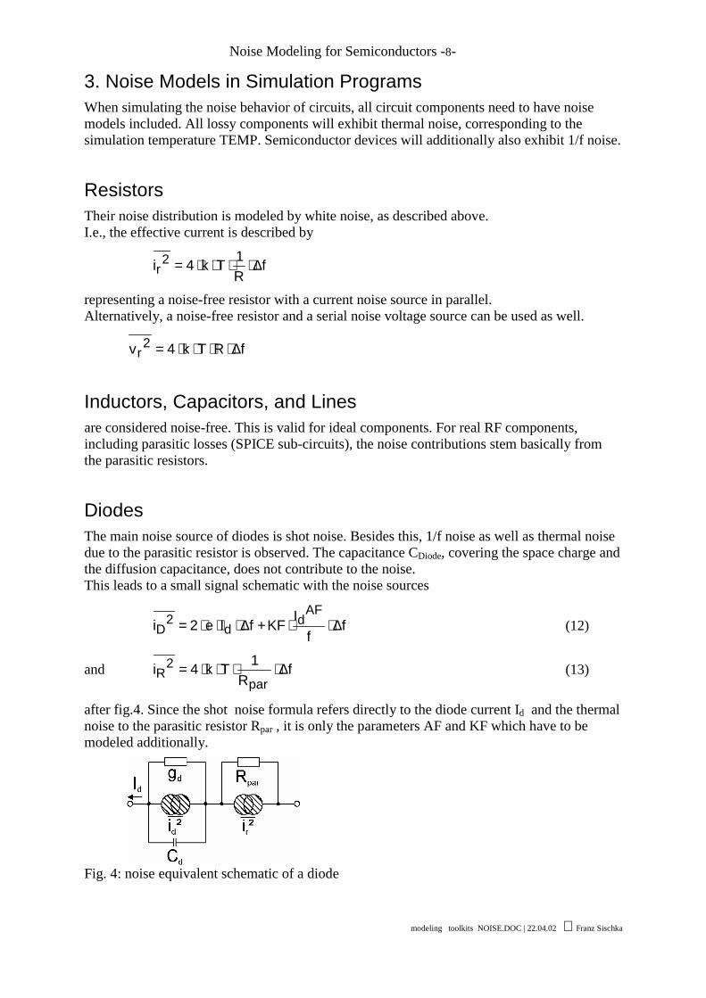
3. Noise Models in Simulation ProgramsWhen simulating the noise behavior of circuits, all circuit components need to have noisemodels included. All lossy components will exhibit thermal noise, corresponding to thesimulation temperature TEMP. Semiconductor devices will additionally also exhibit 1/f noise.
ResistorsTheir noise distribution is modeled by white noise, as described above.I.e., the effective current is described by
fR1Tk4i 2
r ∆⋅⋅⋅⋅=
representing a noise-free resistor with a current noise source in parallel.Alternatively, a noise-free resistor and a serial noise voltage source can be used as well.
fRTk4v 2r ∆⋅⋅⋅⋅=
Inductors, Capacitors, and Linesare considered noise-free. This is valid for ideal components. For real RF components,including parasitic losses (SPICE sub-circuits), the noise contributions stem basically fromthe parasitic resistors.
DiodesThe main noise source of diodes is shot noise. Besides this, 1/f noise as well as thermal noisedue to the parasitic resistor is observed. The capacitance CDiode, covering the space charge andthe diffusion capacitance, does not contribute to the noise.This leads to a small signal schematic with the noise sources
ff
IKFfIe2iAF
dd
2D ∆⋅⋅+∆⋅⋅⋅= (12)
and fR
1Tk4ipar
2R ∆⋅⋅⋅⋅= (13)
after fig.4. Since the shot noise formula refers directly to the diode current Id and the thermalnoise to the parasitic resistor Rpar , it is only the parameters AF and KF which have to bemodeled additionally.
Fig. 4: noise equivalent schematic of a diode
Noise Modeling for Semiconductors -9-
modeling toolkits NOISE.DOC | 22.04.02 Franz Sischka
Bipolar TransistorsSPICE and similar simulators feature a noise schematic for bipolar transistors after fig.5.
Fig.5: noise schematic of a bipolar transistor.
Associated with each physical resistor (Rb at the Base, Rc at the Collector and Re at theEmitter), is a thermal noise source
fR1Tk4ii
2i,R ∆⋅⋅⋅⋅= , i = b, c, e (14)
Base and Collector currents are considered to be independent. Therefore, the shot noise can bedescribed by a source
fIe2i b2
S,b ∆⋅⋅⋅= (15)
at the Base and
fIe2ii c2
nc2
S,c ∆⋅⋅⋅== (16)
at the Collector. The total 1/f noise of the transistors is described by a noise source in parallelwith the Base-Emitter contact. This leads to the noise source at the Base following
ff
IKFfIe2iAF
bb
2nb ∆⋅⋅+∆⋅⋅⋅= (17)
with, again, the noise model parameters AF and KF.
Agilent's Advanced Design System (ADS) include with the BJT transistor model additionallya generation/recombination noise effect in the noise spectrum of the Base. Referring to equ.(17), this means
f
FBf1
IKBff
IKFfIe2i2
ABb
AFb
b
BJT,ADS2
nb ∆⋅
+
⋅+∆⋅⋅+∆⋅⋅⋅=
(18)
Noise Modeling for Semiconductors -10-
modeling toolkits NOISE.DOC | 22.04.02 Franz Sischka
with the new model parameters KB, AB and FB.
With PSPICE, the Collector current ic includes an additional 1/f noise source. This gives
ff
IKFfIe2i
AFc
cPSPICE
2nc ∆⋅⋅+∆⋅⋅⋅=
(19)
using the same parameters KF and AF of the Base contact.
The VBIC model for bipolar transistors [6] includes, similar to the UCB SPICE BJT model,thermal noise sources as well as shot noise for the Base-Emitter current and the transportcurrent. The 1/f noise is described again by a noise source between Base and Emitter. With
ff
IKFfIe2i BF
AFb
bVBIC
2nb ∆⋅⋅+∆⋅⋅⋅=
(20)
however, the frequency dependence is additionally modeled by the parameter BF. Besides themain NPN transistor, VBIC includes also a parasitic PNP transistor. Its noise contribution ismodeled in analogy to the NPN, sharing the same model parameters for the 1/f noise. Moredetails can be found in [7,8].
Noise in the MEXTRAM model is described like with the SPICE BJT model [9]. Besidesthermal noise, there are shot noise sources associated with the Base-Emitter current as well asthe transport current.. 1/f noise is described after (17).
Junction FETsThe noise schematic of field effect transistors is most often like in fig.6 [3].
Fig.6: Noise equivalent schematic for field effect transistors
The noise behavior is described by four noise sources. The resistors RD and RS are associatedwith thermal noise after
fR1Tk4iD
2RD ∆⋅⋅⋅⋅= (21)
and fR1Tk4iS
2RS ∆⋅⋅⋅⋅= (22)
Noise Modeling for Semiconductors -11-
modeling toolkits NOISE.DOC | 22.04.02 Franz Sischka
The amplifier effect of JFETs is based on changes in the channel resistor. This leads todescribing the noise of the channel current ID also by thermal noise
fgTk38i m
2th,nD ∆⋅⋅⋅⋅= (23)
Additionally, an 1/f noise source is assumed with the channel after
ff
IKFfgTk38i
AFD
m2
nD ∆⋅⋅+∆⋅⋅⋅⋅= (24)
with the model parameters AF and KF. The shot noise of the Gate current is usuallyneglected.
This model is valid for the simulators SPICE2, SPICE3, PSPICE and ADS. With HSPICE, anadditional series resistor at the Gate is assumed with corresponding thermal noise. For thethermal noise of the channel, there is a choice to replace equ.(23) by a more accurate model[3].
With ( ) fGDSNOI1
1VvTk38i
20Tgs
HSPICE2
th,nD ∆⋅⋅α+α+α+⋅−⋅β⋅⋅⋅=
(25)
and
−−
=α,regionsaturation0
regionlinearVv
v10Tgs
ds
(26)
it differentiates between linear and saturated region. And, with GDSNOI , an additional noiseparameter is introduced.
MOSFETSThe noise formulation of MOSFET models in most of the commonly used simulationprograms is based on the SPICE2 model of the UCB University of California, Berkeley,described in [3]. It is known, however, that the thermal channel noise included in this modelis essentially valid only in the saturated region of the output characteristics [11]. Therefore,the latest UCB model, the BSIM3v3 model [10], models the noise differently, see furtherbelow.
Fig.7 depicts the noise equivalent schematic of the SPICE2 MOS2 and MOS3 model. Likewith the JFET transistor, the resistors RD and RS are associated with thermal noise after
fR1Tk4id
2Rd ∆⋅⋅⋅⋅= (27)
and fR1Tk4is
2Rs ∆⋅⋅⋅⋅= (28)
The channel noise is described by
fLCf
IKFfgTk38i 2
effox
AFD
m2
nD ∆⋅⋅⋅
⋅+∆⋅⋅⋅⋅= (29)
Noise Modeling for Semiconductors -12-
modeling toolkits NOISE.DOC | 22.04.02 Franz Sischka
using again the parameters AF and KF for the flicker noise. Cox and Leff are calculated insidethe model from the other model parameters.
Fig.7: Noise equivalent schematic of the SPICE2 MOS level2 and level3 transistor model.
In PSPICE, an additional thermal noise of the Gate and of the Bulk resistor is included. WithADS, the models MOSFET Level 1-3 and EEMOS1 are also based on fig.7. With EEMOS1,however, no 1/f noise is included.. With HSPICE, like with the mentioned JFETs fromabove, the user has the choice between this and an alternate noise description. The thermalchannel noise is described again after equ. (25), with the exception
−=α
regionsaturationthein0
regionlineartheinV
v1sat,D
ds
(30)
With the BSIM3v3 model of UCB SPICE3, the user can select for both, the flicker noise aswell as for the thermal channel noise, one of the following models. This is done by setting themodel parameter noimod accordingly. Either, a slightly modified SPICE2 model describes the1/f noise by
fLCf
IKFi 2effox
EF
AFD2
f1 ∆⋅⋅⋅
⋅= (31)
Here, with the same functionality like in the VBIC bipolar model, an additional parameter EFhas been introduced, modeling the frequency dependence of the noise spectrum. The thermalchannel noise is calculated in BSIM3v3 after
( ) fgggTk38i mbdsm
2th ∆⋅++⋅⋅⋅= (32)
Or, depending on the parameter NOIMOD, the BSIM3v3 noise model calculates the 1/f noiseafter
( )EM,EF,NOIC,NOIB,NOIAfi 2f1 = (33)
using a relatively complex formula, and involving the five new noise parameters NOIA,NOIB, NOIC, EF and EM as well as large signal model parameters [34].
Noise Modeling for Semiconductors -13-
modeling toolkits NOISE.DOC | 22.04.02 Franz Sischka
For the channel noise, it is
fQL
Tk4i inv2eff
eff2th ∆⋅⋅
µ⋅⋅⋅= (34)
with ( )
⋅
⋅+⋅−⋅⋅⋅⋅−= dseff
tgsteffbulk
gsteffoxeffeffinv Vv2V2
A1VCLWQ
(35)
The procedure described further below in this paper, covering the 1/f noise parameterextraction, can therefore be applied to the BSIM3v3 model only if the SPICE2 model for the1/f noise has been selected specifically by the parameter NOIMOD. For extracting theparameters NOIA, NOIB, NOIC, EF and EM, see the BSIM3v3 toolkit for IC-CAP.
MESFETSThe noise behavior of MESFETs is modeled in the simulation programs PSPICE andHSPICE essentially analogous to the corresponding JFET -models [3]. See [12] for moredetails.
As a final remark, the noise bandwidth ∆f is set to ∆f=1Hz in most simulators.
Noise Modeling for Semiconductors -14-
modeling toolkits NOISE.DOC | 22.04.02 Franz Sischka
4. 1/f Noise Measurement SetupWhen measuring noise of high frequency transistors, we continue to distinguish between alow frequency range up to several MHz, followed then by a second range up to the maximumoperating frequency of the device (GHz). In the first range, the noise power density spectrumis measured in order to characterize the 1/f noise and the generation/recombination noise. Inthe upper range, the noise figure Fmin, and the parameters Rn , Yopt are measured.
We will now discuss a possible measurement setup for the first range, the 1/f noisecharacteristics. It is depicted in figure 8. It consists of an HP4142 or HP415x SMU, which,however, is operated in ‘power supply’ mode. This means that it is triggered to output either acurrent or voltage (depending on the type of transistor), and to keep this current or voltageswitched on, until the 1/f noise measurement is over and a new 'stop' command is sent to theSMU. The SMU is connected to the Gate or Base of the transistor by a 1Hz filter. Its outputresistance is switchable. For MOS transistors, a low output impedance of the filter is required(e.g. 50Ω), while a high output impedance (e.g. 500kΩ) is used for bipolar transistors.Note: for a bipolar transistor, the 1/f noise is generated in the Base region. If the 1Hz filterhad a low output impedance, it would shorten this noise source and we wouldmeasure/simulate a too low 1/f noise characteristic. The higher the 1Hz filter's outputimpedance is, the less shortening occurs, see also [14]. In the toolkit, a value of ~330kΩ hasbeen found to work best.
The output of the transistor is connected to a special low-noise current amplifier. Besidesamplifying the 1/f noise, this amplifier also serves to bias the Drain or Collector of thetransistor, and also to compensate the DC Drain or Collector current with an ultra-low noiseDC current source. This allows to amplify only the noise current of the transistor:
With this setup, the cabling is minimized. Only 2 short coax cables are used to bias thetransistor and to measure the noise. Therefore, extremely reliable and extremely clean noisemeasurements are obtained.The output of the noise amplifier is further connected to an HP35670 dynamic signalanalyzer, which then converts the 1/f noise time signals into a frequency spectrum.The whole setup is controlled by special IC-CAP macros for bipolar transistors, and for MOStransistors. Ready-to-use extraction routines for the noise parameters AF, KF and EF (forMOS) are included as well.
2transistor_noise
22amplifier_output IRV ⋅=
Noise Modeling for Semiconductors -15-
modeling toolkits NOISE.DOC | 22.04.02 Franz Sischka
Stanford Research SR570Low noise current amplifier
Both, Id (Ic) and R are adjusted. Id (Ic), to prevent the transresistance amplifier from saturation, and R for gain at minimal amplifier noise. Note: The amplifier noise is minimum if R=Rds (or Rce).
For lowest 50Hz noise, theamplifier is battery powered.
1Hzlowpass
SMU
Id or Ic
-+
RIt was found that a 4142 or 415x SMU is ok for Gate or Base biasing. No 50Hz or SMU noise was observed.
Vd or Vc
Vg or Ib
triax
coaxto3.5mmcableusingGSGprobes
coax
Agi
lent
356
70
3.5mmto coaxcableusingGSGprobes
Fig.8a: Block diagram of the 1/f noise measurement setup of the IC-CAP toolkit
Note: For on-wafer measurements, special attention has to be paid regarding shielding. It isrecommended to use a prober with a special 1/f shielding. However, most important, it isrecommended to use the G-S-G RF probes instead of using DC probes !
all capacitor symbols represent:(for NPN and PNP transistors)
from SMU to GSG probe(transistor)
4.7kΩ 50ΩRout4.7kΩ4.7kΩ
The filter is required for biasing the transistor input.It offers -60dB attenuation at 50Hz.
Required Output Impedance for DUT (to avoid shortening the 1/f transistor noise):Rout =330 kΩ for bipolar, 50 Ω for MOS transistor
+--+
100uFelectrolyte
each10nFtantal
metal film resistors!
Fig.8b: 1Hz DC bias filter
Noise Modeling for Semiconductors -16-
modeling toolkits NOISE.DOC | 22.04.02 Franz Sischka
SETUP SR570
1Hz Filter
fromSMU
to35670
Fig.8c: The measurement setup
Noise Modeling for Semiconductors -17-
modeling toolkits NOISE.DOC | 22.04.02 Franz Sischka
The 1/f noise modeling toolkit contains all required IC-CAP measurement setups and drivermacros for measuring the bipolar and MOS transistor 1/f noise and to extract the modelparameters. Fig.9 shows its structure, and fig.10 the macros for measurements and parameterextractions.
Fig. 9: structure of the 1/f noise modeling toolkit.
Fig.10: toolkit macros for controlling the measurements and the extractions
Measurement resolution of the setup of fig.8:
The current noise spectral density resolution obtainable with this system has been measured as~5E-21 A2/Hz.
Noise Modeling for Semiconductors -18-
modeling toolkits NOISE.DOC | 22.04.02 Franz Sischka
Noise Modeling for Semiconductors -19-
modeling toolkits NOISE.DOC | 22.04.02 Franz Sischka
5. AF, KF and BF/EF Noise Parameter Extraction andVerification
Considering the parameter extraction, we refer to the method introduced in [13, see also 14].Following this approach, there is no need to exactly determine the corner frequency fc likewith other proposed methods. For the corner frequency fc, the 1/f noise equals the white noise.For frequencies below that, the 1/f noise is dominant, allowing to neglect all other noisesources for the further analysis. The current noise source of the transistor can now becalculated out of the measured noise at the output of the transresistance amplifier.
Bipolar Transistors:
For the bipolar transistor models, the origin of the 1/f noise is the Base region, seeequation (17). However, the effective 1/f current noise spectral density [A2/Hz] is measured atthe Collector of the transistor. Therefore, the 1/f noise at the Base has to be calculated firstafter
⋅
β=
HzAS1S
2iC2
)I(iB
DC_B
(36)
To begin with the parameter extraction, we first repeat the formula of the 1/f effective noisecurrent generated at the Base (equ.17)
[ ]2AF
2f/1nB Af
f
IKFi DC_B ∆⋅⋅= (37)
Note: the VBIC model features an additional 1/f noise parameter, BF, see equ.(20). It acts likethe EF parameter in the BSIM3v3 model: to fit the -10dB/decade slope of the measured 1/fnoise. For details about its extraction, please refer to the next section on MOS transistors.
In order to match equ.(37) to equ.(36), we normalize to ∆f and set ∆f = 1Hz. This gives theBase current noise spectral density
⋅==
HzA
f
IKF
Hz1i
S2
AF2f/1nB
iBDC_B (38)
Since the 1/f slope is a 'given' for our actual modeling problem, our next step is to get rid of itby multiplying the measured curve with the frequency points 'f'. This results in a flat tracewhere we had the 1/f slope before.
AFiB DC_B
IKFfS ⋅=⋅ (39)
Noise Modeling for Semiconductors -20-
modeling toolkits NOISE.DOC | 22.04.02 Franz Sischka
The advantage of this method is that we are now easily able to identify the value of the 1/fnoise at 1Hz, what will be used in the next step. The 1Hz noise value is simply calculated asthe mean value of a maximum flat sub-range of these so transformed data.
Considering the extrapolated measurement result at 1Hz, the above formula simplifies toAF
Hz1@iB DC_BIKFS ⋅= (40)
This means, we are now ready to obtain an 1Hz value of our 1/f noise for each bias conditionIB_DC.
In the next step, we draw these values against the bias current. We apply a logarithmicconversion to the above formula and obtain
and the DC bias current at the Base is transformed by ( )DC_B10 Ilogx =
A linear regression is applied, which returns the y-intersect 'a' and the slope 'b' of a best fittingline for equ.(42).
The noise parameters AF and KF are then calculated after
bAF = (43)
and a10KF = (44)
Noise Modeling for Semiconductors -21-
modeling toolkits NOISE.DOC | 22.04.02 Franz Sischka
Step-by-step modeling procedure for bipolar transistors:
1.) for a first DC bias condition (e.g. iB_DC = 1uA, vCE = 2V), the 1/f noise spectraldensity is measured. As stated above, for the bipolar transistor, the 1Hz Base filter's outputimpedance is set to a high value, e.g. 330kΩ.
NOTE: This value must be considerably bigger than the input resistance DC_B
DC_BEBE i
vr
∂∂
= .
Otherwise, it would shorten the 1/f noise current source inB2 at the Base!
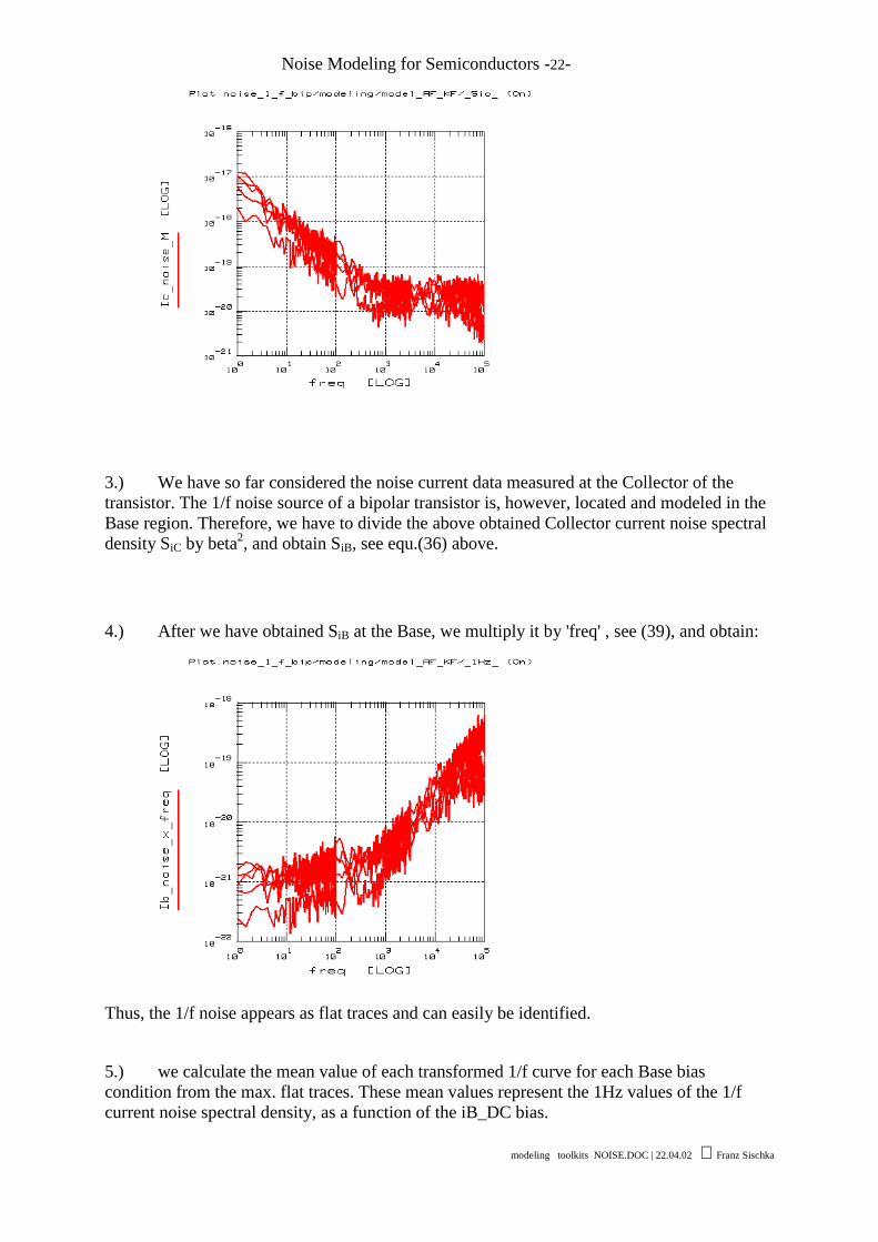
The following plot shows the measured noise current at the Collector:
2.) this is repeated for e.g. 5 more different Base currents, but the same vCE.And we get five 1/f noise curves for each iB_DC bias condition:
Noise Modeling for Semiconductors -22-
modeling toolkits NOISE.DOC | 22.04.02 Franz Sischka
3.) We have so far considered the noise current data measured at the Collector of thetransistor. The 1/f noise source of a bipolar transistor is, however, located and modeled in theBase region. Therefore, we have to divide the above obtained Collector current noise spectraldensity SiC by beta2, and obtain SiB, see equ.(36) above.
4.) After we have obtained SiB at the Base, we multiply it by 'freq' , see (39), and obtain:
Thus, the 1/f noise appears as flat traces and can easily be identified.
5.) we calculate the mean value of each transformed 1/f curve for each Base biascondition from the max. flat traces. These mean values represent the 1Hz values of the 1/fcurrent noise spectral density, as a function of the iB_DC bias.
Noise Modeling for Semiconductors -23-
modeling toolkits NOISE.DOC | 22.04.02 Franz Sischka
6.) Finally, we are ready to draw the 1Hz Base noise data points against the DC biasiB_DC, and fit a line to these data points, see equations (41) and (42).
From the y-intersection and the slope of the fitted curve, we calculate AF and KF afterequations (43) and (44).
7.) After the model parameters have been obtained, the simulation result of the Collectorcurrent noise spectral density is compared with the original measured data, and the AF andKF model parameters are fine-tuned.
Noise Modeling for Semiconductors -24-
modeling toolkits NOISE.DOC | 22.04.02 Franz Sischka
Measured and simulated Collector noise spectral density [A2/Hz] for the bipolar transistor.
Noise Modeling for Semiconductors -25-
modeling toolkits NOISE.DOC | 22.04.02 Franz Sischka
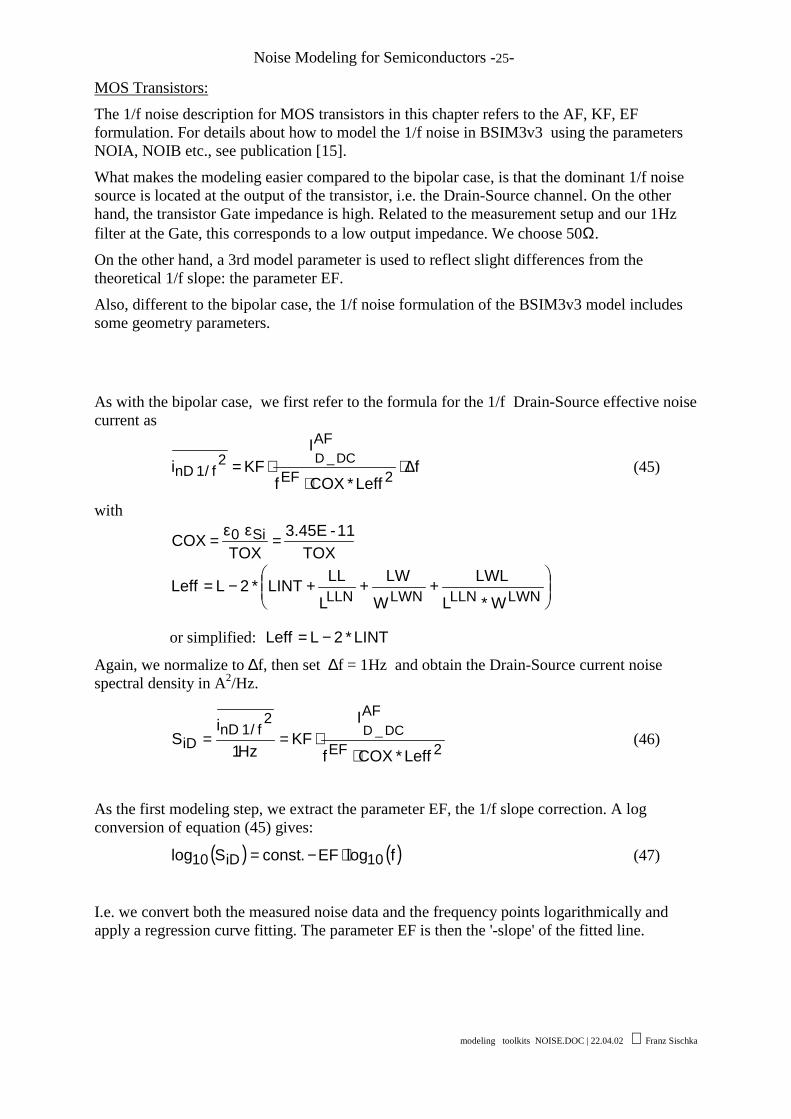
MOS Transistors:
The 1/f noise description for MOS transistors in this chapter refers to the AF, KF, EFformulation. For details about how to model the 1/f noise in BSIM3v3 using the parametersNOIA, NOIB etc., see publication [15].
What makes the modeling easier compared to the bipolar case, is that the dominant 1/f noisesource is located at the output of the transistor, i.e. the Drain-Source channel. On the otherhand, the transistor Gate impedance is high. Related to the measurement setup and our 1Hzfilter at the Gate, this corresponds to a low output impedance. We choose 50Ω.
On the other hand, a 3rd model parameter is used to reflect slight differences from thetheoretical 1/f slope: the parameter EF.
Also, different to the bipolar case, the 1/f noise formulation of the BSIM3v3 model includessome geometry parameters.
As with the bipolar case, we first refer to the formula for the 1/f Drain-Source effective noisecurrent as
fLeff*COXf
IKFi 2EF
AF2
f/1nDDC_D ∆⋅
⋅⋅= (45)
with
TOX11-3.45E
TOX COX Si0 =εε
=
+++−=
LWNLLNLWNLLN W*L
LWL
W
LW
L
LLLINT*2LLeff
or simplified: LINT*2LLeff −=
Again, we normalize to ∆f, then set ∆f = 1Hz and obtain the Drain-Source current noisespectral density in A2/Hz.
2EF
AF2f/1nD
iDLeff*COXf
IKF
Hz1i
S DC_D
⋅⋅== (46)
As the first modeling step, we extract the parameter EF, the 1/f slope correction. A logconversion of equation (45) gives:
( ) ( )flogEF.constSlog 10iD10 ⋅−= (47)
I.e. we convert both the measured noise data and the frequency points logarithmically andapply a regression curve fitting. The parameter EF is then the '-slope' of the fitted line.
Noise Modeling for Semiconductors -26-
modeling toolkits NOISE.DOC | 22.04.02 Franz Sischka
Since the 1/f EF slope is now already modeled, we can get rid of it by multiplying themeasured curve with the frequency points 'f EF'. This results in a flat trace where we had the1/f EF slope in the measurements before.
2
AFEF
iDLeff*COX
IKFfS DC_D⋅=⋅ (48)
After this step, we are again easily able to identify the value of the 1/ f EF noise at 1Hz: it issimply calculated as the mean value of a maximum flat sub-range of these so transformeddata.
Considering the extrapolated measurement result at 1Hz, the above formula simplifies to
2
AF
Hz1@iDLeff*COX
IKFS DC_D⋅= (49)
This means, we are now ready to obtain an 1Hz value of our 1/ f EF noise for each biascondition iD_DC.
In the next step, we draw these values against the iD_DC bias current. We apply a logarithmicconversion to the above formula and obtain
( ) ( )DC_D10210Hz1@iD10 IlogAFLeffCOX
KFlogSlog ⋅+
⋅= (50)
what can be interpreted as a linear function like
xbay ⋅+= (51)
where ( )Hz1@iD10 Slogy =
⋅= 210
LeffCOXKFloga
AFb =and the DC bias current at the Base is transformed by ( )DC_D10 Ilogx =
A linear regression is applied, which returns the y-intersect 'a' and the slope 'b' of a best fittingline.
The noise parameters AF and KF are then calculated after
bAF = (52)
and a2 10LeffCOXKF ⋅⋅= (53)
Noise Modeling for Semiconductors -27-
modeling toolkits NOISE.DOC | 22.04.02 Franz Sischka
Step-by-step modeling procedure for BSIM3v3 CMOS transistors:
1.) for a first DC bias condition (e.g. vG = 0.6V, vDS = 1V), the 1/f Drain current noisespectral density [A2/Hz] is measured. The 1Hz Base filter's output impedance is set to 50Ω.The following plot shows the measurement result:
2.) this is repeated for e.g. 5 more different Gate voltages, but the same vDS.And we get five 1/f noise curves for each vG DC bias condition:
Noise Modeling for Semiconductors -28-
modeling toolkits NOISE.DOC | 22.04.02 Franz Sischka
3.) In the next step, we extract the EF parameter after (47), and check if the slopes of theintermediate simulations match.(Note: the AF and KF have not yet been extracted, therefore only the slopes are important tocompare!)
4.) Now, we are ready to multiply by fEF in order to easier extract the 1Hz value of thenoise.
Noise Modeling for Semiconductors -29-
modeling toolkits NOISE.DOC | 22.04.02 Franz Sischka
5.) we calculate the mean value of each transformed 1/f curve for each vG bias conditionfrom the max. flat regions. These mean values represent the 1Hz values of the 1/f Draincurrent noise spectral density, as a function of the iD_DC bias.
6.) Finally, we are ready to draw the 1Hz Drain current noise data points against the DCbias current iD_DC, and to fit a line to these data points, see equations (50) and (51).
From the y-intersection and the slope of the fitted curve, we calculate AF and KF afterequations (52) and (53)
7.) After the model parameters have been obtained, the simulation result is compared with theoriginal measured data, and the AF, KF and EF model parameters are fine-tuned.
Noise Modeling for Semiconductors -30-
modeling toolkits NOISE.DOC | 22.04.02 Franz Sischka
Measured and simulated Drain current noise spectral density [A2/Hz] for the MOS transistor
NOTE:
The noise data returned from hspice and spice3 differs from the noise data returned fromhpeesofsim, mns, and spectre.hspice and spice3 have units of V^2/Hz and the other simulators have V/Sqrt(Hz).
Noise Modeling for Semiconductors -31-
modeling toolkits NOISE.DOC | 22.04.02 Franz Sischka
Appendix:Noise floor information on the toolkit measurement setup
The figure above shows the current noise density of the system measured at the device output(at the low noise current amplifier LNA).The noise is expressed in A^2/Hz and varies with the LNA sensitivity. The figure shows thenoise floor for the 4 most commonly used values of the LNA sensitivity: 20 uA/V, 50 uA/V,100 uA/V and 200 uA/V.
Comments:• The 1/f noise observed at the beginning of the trace is due to the internal 1/f noise of the
LNA.• The noise drop observed at low sensitivity values (high gain) is due to the bandwidth
limitation of the LNA. Note that this is not in the frequency band used for the extraction(typically between 10 Hz and 1 kHz). Using a sensitivity of 200 uA/V or greater does nothave this limitation but on the other hand, increases the noise floor.
• This noise floor should be compared to the output current noise density of the DUT . If theDUT is a CMOS, this would be the drain current noise density. If the DUT is a bipolar,this should be the collector current noise density. Note that in the bipolar case, the currentnoise source is actually modeled at the input (base current). The Ib noise density isdetermined by dividing the Ic noise density by the DUT current gain (squared).
200 uA/V
20, 50, 100 uA/V
Noise Modeling for Semiconductors -32-
modeling toolkits NOISE.DOC | 22.04.02 Franz Sischka
7. Acknowledgements and Publications
I would like to thank specially F. X. Sinnesbichler of the Technical University Munich,Institute of High Frequency Techniques, for having laid the base for this manual. A big part ofthe chapters stem from this work. I would also especially acknowledge Mr.Sinnesbichler's IC-CAP workshop about Noise modeling in Munich, July 1998.
In the same way, I have to acknowledge Mr.Knoblinger of Infineon Technologies AG inMunich, for his hint on using the special low-noise current amplifier as an excellent andstraight-forward way to measure 1/f noise accurately and without big influences from powerline frequency harmonics.
For important discussions on the noise terminology, I'd like to mention Mr. Berkner, alsoInfineon Technologies AG in Munich.
For detailed verification tests and measurements of the proposed measurement setup I amgrateful to A.Blaum, O.Pilloud, G.Scalea, J.Victory, Motorola, Geneva
Noise Modeling for Semiconductors -33-
modeling toolkits NOISE.DOC | 22.04.02 Franz Sischka
Web InfoStanford Research Web Page: http://www.srsys.com/
[2] B.Schiek, H.-J.Siweris, „Rauschen in Hochfrequenzschaltungen“, Hüthig Buch Verlag,Heidelberg, 1990.
[3] G. Massobrio, P. Antognietti, „Semiconductor Device Modeling with SPICE“, McGraw-Hill, New York, 1993.
[4] F. N. Hooge, „1/f Noise is No Surface Effect“, Physics Letters, Vol. 29A, Nr. 3, pp. 139-194, April 1969.
[5] F. N. Hooge, „1/f Noise Sources“, IEEE Transactions on Electron Devices, Vol. 41,Nr.11, pp. 1926-1935, Nov. 1994.
[6] C. McAndrew at al, „VBIC95: An Improved Vertical, IC Bipolar Transistor Model“,Proceedings of the 1995 BiCMOS Circuits and Technology Meeting, , Minneapolis, pp. 170-177, 1995
[7] C. McAndrew et al, „VBIC95, The Vertical Bipolar Inter-Company Model“, IEEE Journalof Solid-State Circuits, vol. 31, No. 10, pp. 1476-1483, October 1996.
[8] F. X. Sinnesbichler, G. R. Olbrich, „VBIC - The Vertical Bipolar Inter-Company Model.Ein Überblick über das Modell und über zugehörige Parameterextraktionen“, Hewlett-Packard IC-CAP Workshop-Reihe 1997/98, München, Januar 1998.
[9] H. C. deGraaff, F. M. Klaassen, „Compact Transistor Modelling for Circuit Design“,Springer-Verlag, Wien, 1990.
[10] Y. Cheng et al, „BSIM3v3 Manual“, University of California, Berkeley, 1996.
[11] C.C. McAndrew, „Practical Modeling for Circuit Simulation“, IEEE Journal of Solid-State Circuits, vol. 33, no. 3, pp. 439-448, March 1998.
[12] A. Cappy, „Noise Modeling and Measurement Techniques“, IEEE Transactions onMicrowave Theory and Techniques, vol. 36, no. 1pp., 1-10, Jan. 1988.
[13] F. X. Sinnesbichler, M. Fischer, G. R. Olbrich, „Accurate Extraction Method for 1/f-Noise Parameters Used in Gummel-Poon Type Bipolar Junction Transistor Models“, IEEEMTT-S Symposium, Baltimore, 1998, pp. 1345-1348.
[14] J. C. Costa, D. Ngo, R. Jackson, N. Camilleri, J. Jaffee, „Extraction of 1/f NoiseCoefficients for BJTs“, IEEE Transactions on Electron Devices, vol. 40, no. 11, pp.1992-1999, Nov. 1994.
[15] J.C.Vildeuil, M.Valenza, D.Rigaud, Universite de MontpellierII, France, CMOS 1/fNoise Modeling and Extraction of BSIM3 Parameters Using a New Extraction ProcedureICMTS1999 Conference Gothenburg, March 15-18,1999, ISBN 0-7803-5270-X
Noise Modeling for Semiconductors -34-
modeling toolkits NOISE.DOC | 22.04.02 Franz Sischka
[16] C.G.Jakobson, I.Bloom, Y.Nemirovsky, 1/f Noise in CMOS Transistors for AnalogApplications, 19. Convention of Electrical and Electronics Engineers in Israel, 1996, pp.557-560
[17] A.Blaum, O.Pilloud, G.Scalea, J.Victory, F.Sischka, A New Robust On-Wafer 1/f NoiseMeasurement and Characterization System, ICMTS conference 2001,Kobe, Japan, March 19-22,2001
The use of the SR560 low-noise voltage amplifier (lower system noise, but no internal DCbias available) is published in:Hardy et al., Low-Frequency Noise in Proton Damaged LDD MOSFET's,IEEE Trans. on el. devices, vol.46, no.7, July 1999, P.1341
Noise Modeling for Semiconductors -35-
modeling toolkits NOISE.DOC | 22.04.02 Franz Sischka
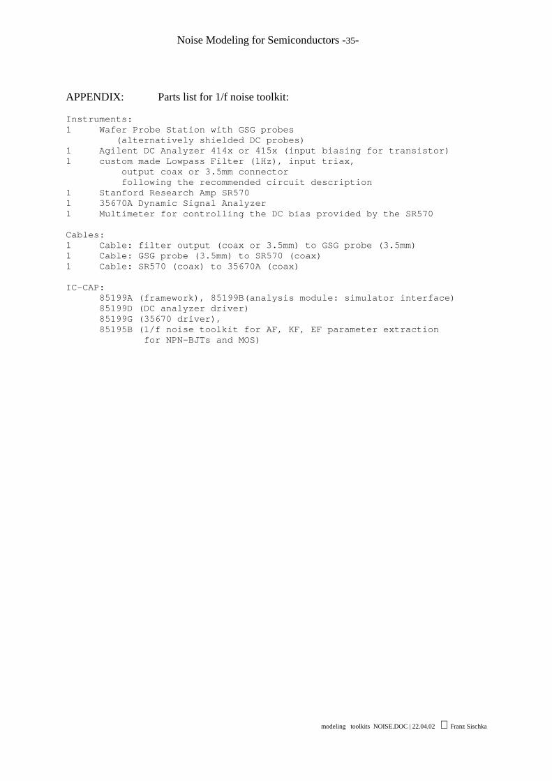
APPENDIX: Parts list for 1/f noise toolkit:
Instruments:1 Wafer Probe Station with GSG probes
(alternatively shielded DC probes)1 Agilent DC Analyzer 414x or 415x (input biasing for transistor)1 custom made Lowpass Filter (1Hz), input triax,
output coax or 3.5mm connectorfollowing the recommended circuit description
1 Stanford Research Amp SR5701 35670A Dynamic Signal Analyzer1 Multimeter for controlling the DC bias provided by the SR570
Cables:1 Cable: filter output (coax or 3.5mm) to GSG probe (3.5mm)1 Cable: GSG probe (3.5mm) to SR570 (coax)1 Cable: SR570 (coax) to 35670A (coax)
IC-CAP:85199A (framework), 85199B(analysis module: simulator interface)85199D (DC analyzer driver)85199G (35670 driver),85195B (1/f noise toolkit for AF, KF, EF parameter extraction