• ORG pin to select word size for ‘46C’ version• 128 x 8-bit organization ‘A’ version devices
(no ORG)• 64 x 16-bit organization ‘B’ version devices
(no ORG)• Self-timed erase/write cycles (including
auto-erase)• Automatic ERAL before WRAL• Power-on/off data protection circuitry
• Industry standard 3-wire serial I/O• Device Status signal (Ready/Busy)• Sequential read function
• 1,000,000 E/W cycles• Data retention > 200 years• Temperature ranges supported:
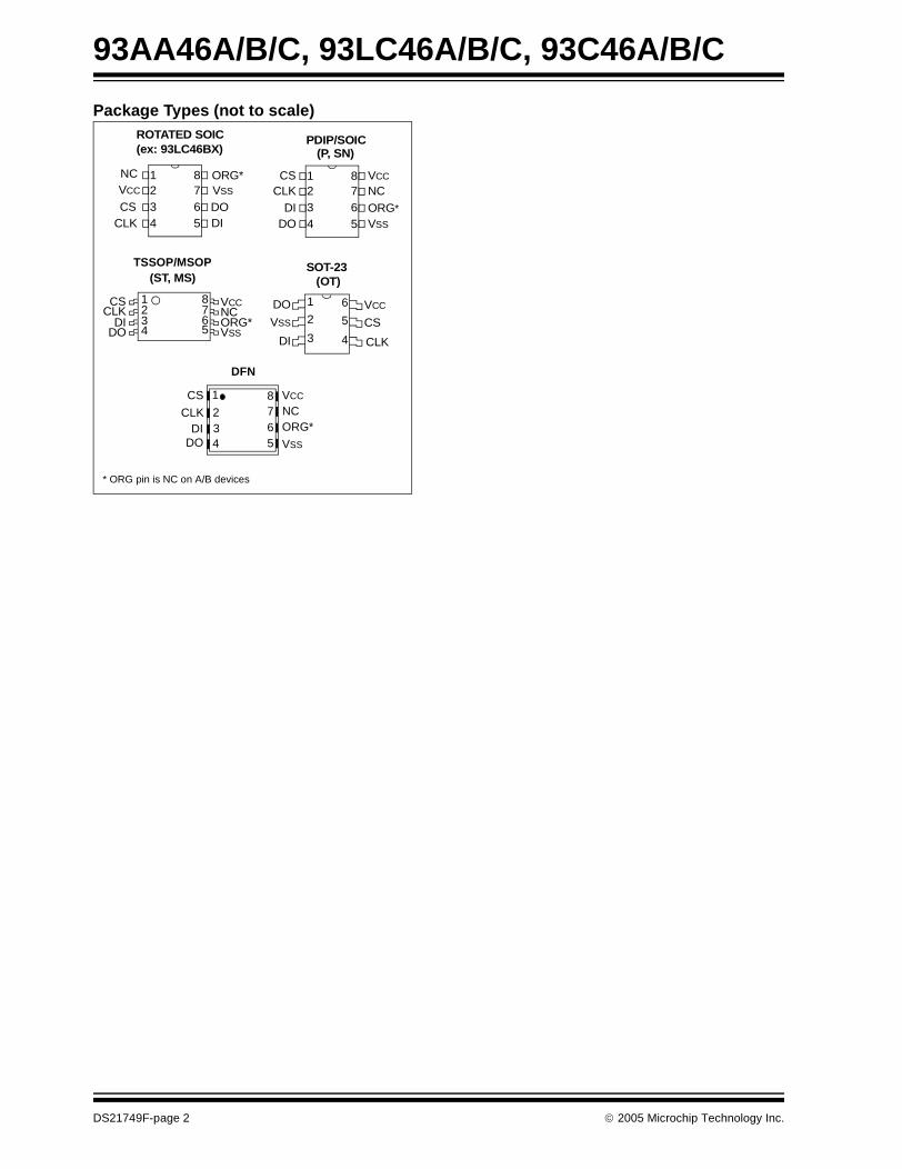
Pin Function Table
Description:
The Microchip Technology Inc. 93XX46A/B/C devicesare 1K bit low-voltage serial Electrically ErasablePROMs (EEPROM). Word-selectable devices such asthe 93AA46C, 93LC46C or 93C46C are dependentupon external logic levels driving the ORG pin to setword size. For dedicated 8-bit communication, the93AA46A, 93LC46A or 93C46A devices are available,while the 93AA46B, 93LC46B and 93C46B devicesprovide dedicated 16-bit communication. AdvancedCMOS technology makes these devices ideal for lowpower, nonvolatile memory applications. The entire93XX Series is available in standard packages includ-ing 8-lead PDIP and SOIC, and advanced packagingincluding 8-lead MSOP, 6-lead SOT-23, 8-lead 2x3DFN and 8-lead TSSOP. Pb-free (Pure Matte Sn) finishis also available.
Part Number VCC Range ORG Pin Word Size Temp Ranges Packages
93AA46A 1.8-5.5 No 8-bit I P, SN, ST, MS, OT, MC
93AA46B 1.8-5-5 No 16-bit I P, SN, ST, MS, OT, MC
93LC46A 2.5-5.5 No 8-bit I, E P, SN, ST, MS, OT, MC
93LC46B 2.5-5.5 No 16-bit I, E P, SN, ST, MS, OT, MC
93C46A 4.5-5.5 No 8-bit I, E P, SN, ST, MS, OT, MC
93C46B 4.5-5.5 No 16-bit I, E P, SN, ST, MS, OT, MC
93AA46C 1.8-5.5 Yes 8 or 16-bit I P, SN, ST, MS, MC
93LC46C 2.5-5.5 Yes 8 or 16-bit I, E P, SN, ST, MS, MC
93C46C 4.5-5.5 Yes 8 or 16-bit I, E P, SN, ST, MS, MC
All inputs and outputs w.r.t. VSS ..........................................................................................................-0.6V to VCC +1.0V
Storage temperature ............................................................................................................................... -65°C to +150°C
Ambient temperature with power applied................................................................................................-40°C to +125°C
ESD protection on all pins ......................................................................................................................................................≥ 4 kV
TABLE 1-1: DC CHARACTERISTICS
† NOTICE: Stresses above those listed under “Absolute Maximum Ratings” may cause permanent damage tothe device. This is a stress rating only and functional operation of the device at those or any other conditionsabove those indicated in the operational listings of this specification is not implied. Exposure to maximum ratingconditions for extended periods may affect device reliability.
All parameters apply over the specified ranges unless otherwise noted.
Industrial (I): TA = -40°C to +85°C, VCC = +1.8V TO +5.5VAutomotive (E): TA = -40°C to +125°C, VCC = +2.5V TO +5.5V
Note 1: This parameter is periodically sampled and not 100% tested.
2: This application is not tested but ensured by characterization. For endurance estimates in a specificapplication, please consult the Total Endurance™ Model which may be obtained from Microchip’s web siteat www.microchip.com.
When the ORG pin (93XX46C) is connected to VCC,the (x16) organization is selected. When it is connectedto ground, the (x8) organization is selected. Instruc-tions, addresses and write data are clocked into the DIpin on the rising edge of the clock (CLK). The DO pin isnormally held in a High-Z state except when readingdata from the device, or when checking the Ready/Busy status during a programming operation. TheReady/Busy status can be verified during an erase/write operation by polling the DO pin; DO low indicatesthat programming is still in progress, while DO highindicates the device is ready. DO will enter the High-Zstate on the falling edge of CS.
2.1 Start Condition
The Start bit is detected by the device if CS and DI areboth high with respect to the positive edge of CLK forthe first time.
Before a Start condition is detected, CS, CLK and DImay change in any combination (except to that of aStart condition), without resulting in any deviceoperation (Read, Write, Erase, EWEN, EWDS, ERALor WRAL). As soon as CS is high, the device is nolonger in Standby mode.
An instruction following a Start condition will only beexecuted if the required opcode, address and data bitsfor any particular instruction are clocked in.
2.2 Data In/Data Out (DI/DO)
It is possible to connect the Data In and Data Out pinstogether. However, with this configuration it is possiblefor a “bus conflict” to occur during the “dummy zero”that precedes the read operation, if A0 is a logic highlevel. Under such a condition the voltage level seen atData Out is undefined and will depend upon the relativeimpedances of Data Out and the signal source drivingA0. The higher the current sourcing capability of A0,the higher the voltage at the Data Out pin. In order tolimit this current, a resistor should be connectedbetween DI and DO.
2.3 Data Protection
All modes of operation are inhibited when VCC is belowa typical voltage of 1.5V for '93AA' and '93LC' devicesor 3.8V for '93C' devices.
The EWEN and EWDS commands give additionalprotection against accidentally programming duringnormal operation.
After power-up, the device is automatically in theEWDS mode. Therefore, an EWEN instruction must beperformed before the initial ERASE or WRITE instructioncan be executed.
Block Diagram
Note: When preparing to transmit an instruction,either the CLK or DI signal levels must beat a logic low as CS is toggled active high.
Note: For added protection, an EWDScommand should be performed afterevery write operation and an external 10kΩ pull-down protection resistor should beadded to the CS pin.
The ERASE instruction forces all data bits of thespecified address to the logical ‘1’ state. CS is broughtlow following the loading of the last address bit. Thisfalling edge of the CS pin initiates the self-timedprogramming cycle, except on ‘93C’ devices where therising edge of CLK before the last address bit initiatesthe write cycle.
The DO pin indicates the Ready/Busy status of thedevice if CS is brought high after a minimum of 250 nslow (TCSL). DO at logical ‘0’ indicates that programmingis still in progress. DO at logical ‘1’ indicates that theregister at the specified address has been erased andthe device is ready for another instruction.
FIGURE 2-1: ERASE TIMING FOR 93AA AND 93LC DEVICES
FIGURE 2-2: ERASE TIMING FOR 93C DEVICES
Note: After the Erase cycle is complete, issuinga Start bit and then taking CS low will clearthe Ready/Busy status from DO.
The Erase All (ERAL) instruction will erase the entirememory array to the logical ‘1’ state. The ERAL cycleis identical to the erase cycle, except for the differentopcode. The ERAL cycle is completely self-timed andcommences at the falling edge of the CS, except on‘93C’ devices where the rising edge of CLK before thelast data bit initiates the write cycle. Clocking of theCLK pin is not necessary after the device has enteredthe ERAL cycle.
The DO pin indicates the Ready/Busy status of thedevice, if CS is brought high after a minimum of 250 nslow (TCSL).
VCC must be ≥ 4.5V for proper operation of ERAL.
FIGURE 2-3: ERAL TIMING FOR 93AA AND 93LC DEVICES
FIGURE 2-4: ERAL TIMING FOR 93C DEVICES
Note: After the ERAL command is complete,issuing a Start bit and then taking CS lowwill clear the Ready/Busy status from DO.
The 93XX46A/B/C powers up in the Erase/Write Disable(EWDS) state. All Programming modes must bepreceded by an Erase/Write Enable (EWEN) instruction.Once the EWEN instruction is executed, programmingremains enabled until an EWDS instruction is executed orVcc is removed from the device.
To protect against accidental data disturbance, the EWDSinstruction can be used to disable all erase/write functionsand should follow all programming operations. Executionof a READ instruction is independent of both the EWEN andEWDS instructions.
FIGURE 2-5: EWDS TIMING
FIGURE 2-6: EWEN TIMING
2.7 Read
The READ instruction outputs the serial data of theaddressed memory location on the DO pin. A dummyzero bit precedes the 8-bit (if ORG pin is low or A-Versiondevices) or 16-bit (if ORG pin is high or B-versiondevices) output string.
The output data bits will toggle on the rising edge of theCLK and are stable after the specified time delay (TPD).Sequential read is possible when CS is held high. Thememory data will automatically cycle to the next registerand output sequentially.
The WRITE instruction is followed by 8 bits (if ORG islow or A-version devices) or 16 bits (if ORG pin is highor B-version devices) of data which are written into thespecified address. For 93AA46A/B/C and 93LC46A/B/Cdevices, after the last data bit is clocked into DI, thefalling edge of CS initiates the self-timed auto-erase andprogramming cycle. For 93C46A/B/C devices, the self-timed auto-erase and programming cycle is initiated bythe rising edge of CLK on the last data bit.
The DO pin indicates the Ready/Busy status of thedevice, if CS is brought high after a minimum of 250 nslow (TCSL). DO at logical ‘0’ indicates that programmingis still in progress. DO at logical ‘1’ indicates that theregister at the specified address has been written withthe data specified and the device is ready for anotherinstruction.
FIGURE 2-8: WRITE TIMING FOR 93AA AND 93LC DEVICES
FIGURE 2-9: WRITE TIMING FOR 93C DEVICES
Note: After the Write cycle is complete, issuing aStart bit and then taking CS low will clearthe Ready/Busy status from DO.
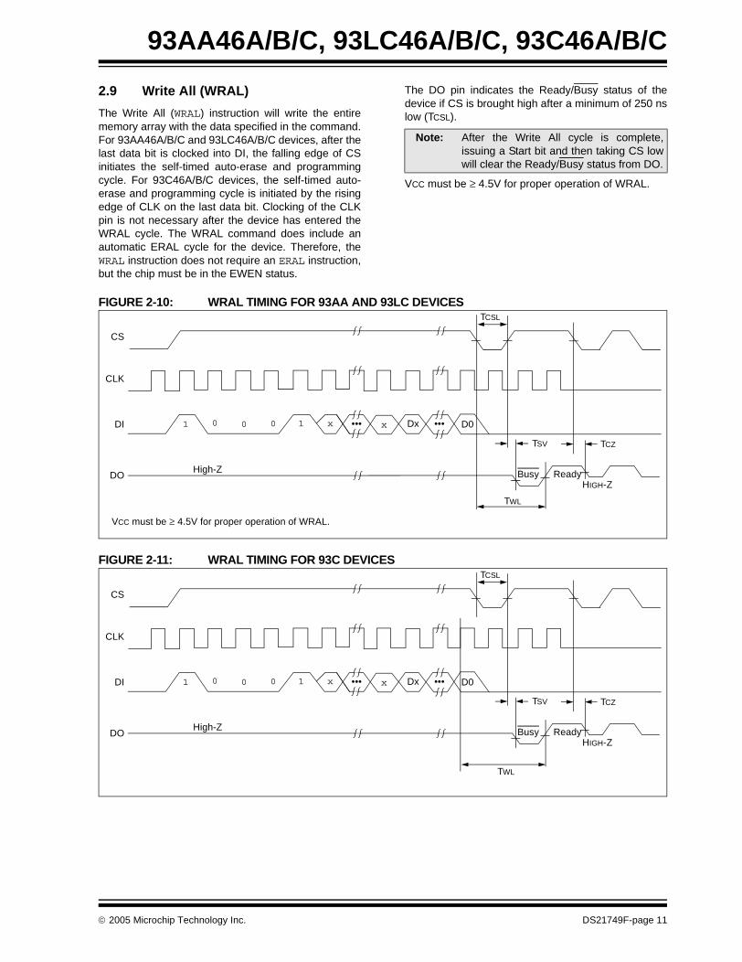
The Write All (WRAL) instruction will write the entirememory array with the data specified in the command.For 93AA46A/B/C and 93LC46A/B/C devices, after thelast data bit is clocked into DI, the falling edge of CSinitiates the self-timed auto-erase and programmingcycle. For 93C46A/B/C devices, the self-timed auto-erase and programming cycle is initiated by the risingedge of CLK on the last data bit. Clocking of the CLKpin is not necessary after the device has entered theWRAL cycle. The WRAL command does include anautomatic ERAL cycle for the device. Therefore, theWRAL instruction does not require an ERAL instruction,but the chip must be in the EWEN status.
The DO pin indicates the Ready/Busy status of thedevice if CS is brought high after a minimum of 250 nslow (TCSL).
VCC must be ≥ 4.5V for proper operation of WRAL.
FIGURE 2-10: WRAL TIMING FOR 93AA AND 93LC DEVICES
FIGURE 2-11: WRAL TIMING FOR 93C DEVICES
Note: After the Write All cycle is complete,issuing a Start bit and then taking CS lowwill clear the Ready/Busy status from DO.
A high level selects the device; a low level deselectsthe device and forces it into Standby mode. However, aprogramming cycle which is already in progress will becompleted, regardless of the Chip Select (CS) inputsignal. If CS is brought low during a program cycle, thedevice will go into Standby mode as soon as theprogramming cycle is completed.
CS must be low for 250 ns minimum (TCSL) betweenconsecutive instructions. If CS is low, the internalcontrol logic is held in a Reset status.
3.2 Serial Clock (CLK)
The Serial Clock is used to synchronize the communi-cation between a master device and the 93XX seriesdevice. Opcodes, address and data bits are clocked inon the positive edge of CLK. Data bits are also clockedout on the positive edge of CLK.
CLK can be stopped anywhere in the transmissionsequence (at high or low level) and can be continuedanytime with respect to clock high time (TCKH) andclock low time (TCKL). This gives the controlling masterfreedom in preparing opcode, address and data.
CLK is a “don't care” if CS is low (device deselected). IfCS is high, but the Start condition has not beendetected (DI = 0), any number of clock cycles can bereceived by the device without changing its status (i.e.,waiting for a Start condition).
CLK cycles are not required during the self-timed write(i.e., auto erase/write) cycle.
After detection of a Start condition the specified numberof clock cycles (respectively low-to-high transitions ofCLK) must be provided. These clock cycles arerequired to clock in all required opcode, address anddata bits before an instruction is executed. CLK and DIthen become “don't care” inputs waiting for a new Startcondition to be detected.
3.3 Data In (DI)
Data In (DI) is used to clock in a Start bit, opcode,address and data synchronously with the CLK input.
3.4 Data Out (DO)
Data Out (DO) is used in the Read mode to output datasynchronously with the CLK input (TPD after thepositive edge of CLK).
This pin also provides Ready/Busy status informationduring erase and write cycles. Ready/Busy status infor-mation is available on the DO pin if CS is brought highafter being low for minimum Chip Select low time (TCSL)and an erase or write operation has been initiated.
The Status signal is not available on DO, if CS is heldlow during the entire erase or write cycle. In this case,DO is in the High-Z mode. If status is checked after theerase/write cycle, the data line will be high to indicatethe device is ready.
3.5 Organization (ORG)
When the ORG pin is connected to VCC or Logic HI, the(x16) memory organization is selected. When the ORGpin is tied to VSS or Logic LO, the (x8) memoryorganization is selected. For proper operation, ORGmust be tied to a valid logic level.
93XX46A devices are always x8 organization and93XX46B devices are always x16 organization.
Note: T = Temperature grade (I, E)NN = Alphanumeric traceability code
Legend: XX...X Part number or part number codeT Temperature (I, E)Y Year code (last digit of calendar year)YY Year code (last 2 digits of calendar year)WW Week code (week of January 1 is week ‘01’)NNN Alphanumeric traceability code (2 characters for small packages)
Pb-free JEDEC designator for Matte Tin (Sn)
Note: For very small packages with no room for the Pb-free JEDEC designator , the marking will only appear on the outer carton or reel label.
Note: In the event the full Microchip part number cannot be marked on one line, it willbe carried over to the next line, thus limiting the number of availablecharacters for customer-specific information.
3e
3e
Note: Please visit www.microchip.com/Pbfree for the latest information on Pb-free conversion.
*Standard OTP marking consists of Microchip part number, year code, week code, and traceability code.
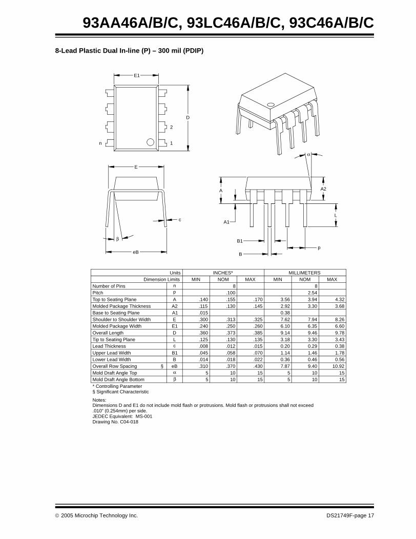
Notes:Dimensions D and E1 do not include mold flash or protrusions. Mold flash or protrusions shall not exceed .010” (0.254mm) per side.JEDEC Equivalent: MS-012Drawing No. C04-057
Notes:Dimensions D and E1 do not include mold flash or protrusions. Mold flash or protrusions shall not exceed .005” (0.127mm) per side.JEDEC Equivalent: MO-153Drawing No. C04-086
Microchip provides online support via our WWW site atwww.microchip.com. This web site is used as a meansto make files and information easily available tocustomers. Accessible by using your favorite Internetbrowser, the web site contains the followinginformation:
• Product Support – Data sheets and errata, application notes and sample programs, design resources, user’s guides and hardware support documents, latest software releases and archived software
• General Technical Support – Frequently Asked Questions (FAQ), technical support requests, online discussion groups, Microchip consultant program member listing
• Business of Microchip – Product selector and ordering guides, latest Microchip press releases, listing of seminars and events, listings of Microchip sales offices, distributors and factory representatives
CUSTOMER CHANGE NOTIFICATION SERVICE
Microchip’s customer notification service helps keepcustomers current on Microchip products. Subscriberswill receive e-mail notification whenever there arechanges, updates, revisions or errata related to aspecified product family or development tool of interest.
To register, access the Microchip web site atwww.microchip.com, click on Customer ChangeNotification and follow the registration instructions.
CUSTOMER SUPPORT
Users of Microchip products can receive assistancethrough several channels:
• Distributor or Representative
• Local Sales Office• Field Application Engineer (FAE)• Technical Support
• Development Systems Information Line
Customers should contact their distributor,representative or field application engineer (FAE) forsupport. Local sales offices are also available to helpcustomers. A listing of sales offices and locations isincluded in the back of this document.
Technical support is available through the web siteat: http://support.microchip.com
In addition, there is a Development SystemsInformation Line which lists the latest versions ofMicrochip’s development systems software products.This line also provides information on how customerscan receive currently available upgrade kits.
The Development Systems Information Linenumbers are:
It is our intention to provide you with the best documentation possible to ensure successful use of your Microchip prod-uct. If you wish to provide your comments on organization, clarity, subject matter, and ways in which our documentationcan better serve you, please FAX your comments to the Technical Publications Manager at (480) 792-4150.
Please list the following information, and use this outline to provide us with your comments about this document.
To: Technical Publications Manager
RE: Reader Response
Total Pages Sent ________
From: Name
Company
Address
City / State / ZIP / Country
Telephone: (_______) _________ - _________
Application (optional):
Would you like a reply? Y N
Device: Literature Number:
Questions:
FAX: (______) _________ - _________
DS21749F93AA46A/B/C, 93LC46A/B/C, 93C46A/B/C
1. What are the best features of this document?
2. How does this document meet your hardware and software development needs?
3. Do you find the organization of this document easy to follow? If not, why?
4. What additions to the document do you think would enhance the structure and subject?
5. What deletions from the document could be made without affecting the overall usefulness?
6. Is there any incorrect or misleading information (what and where)?
To order or obtain information, e.g., on pricing or delivery, refer to the factory or the listed sales office.
Note: Most products manufactured after January 2005 will have a Matte Tin (Pb-free) finish. Most products manufacturedbefore January 2005 will have a finish of approximately 63% Sn and 37% Pb (Sn/Pb). Please visit www.microchip.com/Pbfree for the latest information on Pb-free conversion, including conversion date codes.
Sales and Support
Data Sheets
Products supported by a preliminary Data Sheet may have an errata sheet describing minor operational differencesand recommended workarounds. To determine if an errata sheet exists for a particular device, please contact one ofthe following:
1. Your local Microchip sales office
2. The Microchip Corporate Literature Center U.S. FAX: (480) 792-72773. The Microchip Worldwide Site (www.microchip.com)
Please specify which device, revision of silicon and Data Sheet (include Literature #) you are using.
New Customer Notification System
Register on our web site (www.microchip.com/cn) to receive the most current information on our products.
Device: 93AA46A: 1K 1.8V Microwire Serial EEPROM 93AA46B: 1K 1.8V Microwire Serial EEPROM 93AA46C: 1K 1.8V Microwire Serial EEPROM w/ORG
93LC46A: 1K 2.5V Microwire Serial EEPROM 93LC46B: 1K 2.5V Microwire Serial EEPROM 93LC46C: 1K 2.5V Microwire Serial EEPROM w/ORG
93C46A: 1K 5.0V Microwire Serial EEPROM93C46B: 1K 5.0V Microwire Serial EEPROM93C46C: 1K 5.0V Microwire Serial EEPROM w/ORG
Note the following details of the code protection feature on Microchip devices:
• Microchip products meet the specification contained in their particular Microchip Data Sheet.
• Microchip believes that its family of products is one of the most secure families of its kind on the market today, when used in the intended manner and under normal conditions.
• There are dishonest and possibly illegal methods used to breach the code protection feature. All of these methods, to our knowledge, require using the Microchip products in a manner outside the operating specifications contained in Microchip’s Data Sheets. Most likely, the person doing so is engaged in theft of intellectual property.
• Microchip is willing to work with the customer who is concerned about the integrity of their code.
• Neither Microchip nor any other semiconductor manufacturer can guarantee the security of their code. Code protection does not mean that we are guaranteeing the product as “unbreakable.”
Code protection is constantly evolving. We at Microchip are committed to continuously improving the code protection features of ourproducts. Attempts to break Microchip’s code protection feature may be a violation of the Digital Millennium Copyright Act. If such actsallow unauthorized access to your software or other copyrighted work, you may have a right to sue for relief under that Act.
Information contained in this publication regarding deviceapplications and the like is provided only for your convenienceand may be superseded by updates. It is your responsibility toensure that your application meets with your specifications.MICROCHIP MAKES NO REPRESENTATIONS OR WAR-RANTIES OF ANY KIND WHETHER EXPRESS OR IMPLIED,WRITTEN OR ORAL, STATUTORY OR OTHERWISE,RELATED TO THE INFORMATION, INCLUDING BUT NOTLIMITED TO ITS CONDITION, QUALITY, PERFORMANCE,MERCHANTABILITY OR FITNESS FOR PURPOSE.Microchip disclaims all liability arising from this information andits use. Use of Microchip’s products as critical components inlife support systems is not authorized except with expresswritten approval by Microchip. No licenses are conveyed,implicitly or otherwise, under any Microchip intellectual propertyrights.
The Microchip name and logo, the Microchip logo, Accuron, dsPIC, KEELOQ, microID, MPLAB, PIC, PICmicro, PICSTART, PRO MATE, PowerSmart, rfPIC, and SmartShunt are registered trademarks of Microchip Technology Incorporated in the U.S.A. and other countries.
AmpLab, FilterLab, Migratable Memory, MXDEV, MXLAB, PICMASTER, SEEVAL, SmartSensor and The Embedded Control Solutions Company are registered trademarks of Microchip Technology Incorporated in the U.S.A.
Analog-for-the-Digital Age, Application Maestro, dsPICDEM, dsPICDEM.net, dsPICworks, ECAN, ECONOMONITOR, FanSense, FlexROM, fuzzyLAB, In-Circuit Serial Programming, ICSP, ICEPIC, Linear Active Thermistor, MPASM, MPLIB, MPLINK, MPSIM, PICkit, PICDEM, PICDEM.net, PICLAB, PICtail, PowerCal, PowerInfo, PowerMate, PowerTool, rfLAB, rfPICDEM, Select Mode, Smart Serial, SmartTel, Total Endurance and WiperLock are trademarks of Microchip Technology Incorporated in the U.S.A. and other countries.
SQTP is a service mark of Microchip Technology Incorporated in the U.S.A.
All other trademarks mentioned herein are property of their respective companies.
Microchip received ISO/TS-16949:2002 quality system certification for its worldwide headquarters, design and wafer fabrication facilities in Chandler and Tempe, Arizona and Mountain View, California in October 2003. The Company’s quality system processes and procedures are for its PICmicro® 8-bit MCUs, KEELOQ® code hopping devices, Serial EEPROMs, microperipherals, nonvolatile memory and analog products. In addition, Microchip’s quality system for the design and manufacture of development systems is ISO 9001:2000 certified.