55
FYSMAST1069 Examensarbete 30 hp Februari 2018 1kW Class-E solid state power amplifier for cyclotron RF-source Stefan Book Masterprogrammet i fysik Master Programme in Physics
FYSMAST1069
Examensarbete 30 hpFebruari 2018
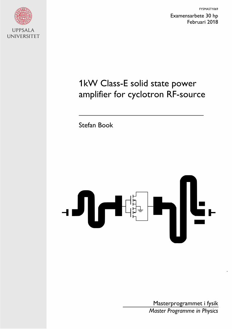
1kW Class-E solid state power amplifier for cyclotron RF-source
Stefan Book
Masterprogrammet i fysikMaster Programme in Physics
Teknisk- naturvetenskaplig fakultet UTH-enheten Besöksadress: Ångströmlaboratoriet Lägerhyddsvägen 1 Hus 4, Plan 0 Postadress: Box 536 751 21 Uppsala Telefon: 018 – 471 30 03 Telefax: 018 – 471 30 00 Hemsida: http://www.teknat.uu.se/student
Abstract
1kW Class-E solid state power amplifier for cyclotronRF-source
Stefan Book
This thesis discusses the design, construction and testing of a highefficiency, 100 MHz, 1 kW, Class-E solid state power amplifier.The design was performed with the aid of computer simulations usingelectronic design software (ADS). The amplifier was constructedaround Ampleon's BLF188XR LDMOS transistor in a single ended design.The results for 100 MHz operation show a power added efficiency of82% at 1200 W pulsed power output.For operation at 102 MHz results show a power added efficiency of 86%at 1050 W pulsed power output.Measurements of the drain- and gate voltage waveforms providevalidation of Class-E operation.
FYSMAST1069Examinator: Andreas KornÄmnesgranskare: Anders RydbergHandledare: Dragos Dancila
Contents
1 Sammanfattning 4
2 Introduction 5
2.1 Background . . . . . . . . . . . . . . . . . . . . . . . . . . . . . . . . 5
2.2 Methodology . . . . . . . . . . . . . . . . . . . . . . . . . . . . . . . 6
2.3 Objective . . . . . . . . . . . . . . . . . . . . . . . . . . . . . . . . . 6
2.4 State-of-the-art . . . . . . . . . . . . . . . . . . . . . . . . . . . . . . 6
3 Theory 8
3.1 RF power ampliers . . . . . . . . . . . . . . . . . . . . . . . . . . . 8
3.2 Stability . . . . . . . . . . . . . . . . . . . . . . . . . . . . . . . . . . 9
3.3 Classes of operation . . . . . . . . . . . . . . . . . . . . . . . . . . . . 10
3.3.1 Biasing and conduction angles . . . . . . . . . . . . . . . . . . 11
3.4 Class E . . . . . . . . . . . . . . . . . . . . . . . . . . . . . . . . . . 13
4 Design and Simulation 16
4.1 The transistor: Ampleon BLF188XR . . . . . . . . . . . . . . . . . . 16
4.2 Frequency of operation . . . . . . . . . . . . . . . . . . . . . . . . . . 16
4.3 Lumped component circuit . . . . . . . . . . . . . . . . . . . . . . . . 17
4.4 Design using transmission lines . . . . . . . . . . . . . . . . . . . . . 22
4.5 Momentum simulations . . . . . . . . . . . . . . . . . . . . . . . . . . 24
4.6 Stability analysis . . . . . . . . . . . . . . . . . . . . . . . . . . . . . 27
5 Amplier construction 28
6 Measurement setup 31
7 Measurements and results 33
7.1 100 MHz performance . . . . . . . . . . . . . . . . . . . . . . . . . . 33
7.2 102 MHz performance . . . . . . . . . . . . . . . . . . . . . . . . . . 36
7.3 Heating . . . . . . . . . . . . . . . . . . . . . . . . . . . . . . . . . . 40
7.4 Input matching . . . . . . . . . . . . . . . . . . . . . . . . . . . . . . 40
8 Conclusions and discussion 41
1

9 Acknowledgments 42
A Appendix A 45
A.1 ADS equations . . . . . . . . . . . . . . . . . . . . . . . . . . . . . . 45
B Appendix B 46
B.1 Electronics at high frequencies . . . . . . . . . . . . . . . . . . . . . . 46
B.1.1 Transmission lines and distributed elements . . . . . . . . . . 47
B.1.2 Reection Coecients . . . . . . . . . . . . . . . . . . . . . . 48
B.1.3 Impedance matching and the Smith chart . . . . . . . . . . . 49
B.1.4 Scattering parameters . . . . . . . . . . . . . . . . . . . . . . 52
2

Abbrevations and Acronyms
AC Alternating Current
dB Decibel
dBm Decibel-milliwatts
DC Direct Current
GaAs Gallium Arsenide
GaN Gallium Nitride
HEMT High Electron Mobility Transistor
HF High Frequency
IDS Drain Source Current
kW Kilo Watts
LDMOS Laterally Diused Metal Oxide Semiconductor
MHz Mega Hertz
PA Power Ampler
PCB Printed Circuit Board
RF Radio Frequency
VDS Drain Source Voltage
VGS Gate Source Voltage
VV SWR Voltage Standing Wave Ratio
3

1 Sammanfattning
Eektförstärkare är en fundamental del av otaliga tillämpningar inom elektronik.
Detta medför ett stort intresse i utvecklingen av eektförstärkare med hög uteekt
och samtidigt hög verkningsgrad, kompakt design och låg produktionskostnad.
En underkategori av eektförstärkare som är av speciellt intresse är switch-mode
förstärkare där transistorn agerar likt en strömbrytare som diskret skiftar mellan
ledande och oledande tillstånd. Denna kategori av eektförstärkare har potential att
uppnå väldigt hög verkningsgrad genom att undvika samtidig ström och spänning i
förstärkarens transistor.
Syftet med detta projekt är att designa, tillverka och mäta en switch-mode eek-
tförstärkare i klass E med en uteekt på 1000 watt och en driftfrekvens på 100
MHz.
Förstärkardesignen genomförs med hjälp av datorsimuleringar och sedan tillverkas
den verkliga förstärkaren för hands. För att utvärdera förstärkarens prestanda mäts
dess uteekt, verkningsrad och förstärkningsfaktor.
Resultaten av detta projekt kan till exempel vara av intresse för partikelacceleratorer
till vetenskapliga och medicinska tillämpningar.
Detta masterarbete är en del av Eurostarsprojektet ENEFRF, ett projekt riktat åt
att utveckla energieektiva eektförstärkare till cyclotroner.
En cyclotron är en typ av partikelaccelerator som kan användas till att accelerera
protoner för att kollidera med syreatomer och därigenom producera radioisotopen
uor-18. Det radioaktiva uoret sönderfaller främst med positronemission, och kan
användas till positronemissionstomogra (PET). Genom att använda en uor-18-
baserad kontrastvätska kan man med PET avgöra plats och storlek hos cancer-
tumörer i en patient [1].
4

2 Introduction
2.1 Background
Power ampliers are a vital part of various electronics applications. For this reason
there is considerable interest in developing power ampliers with high power output
while having high eciencies, compact designs and low manufacturing costs.
A subcategory of power ampliers of particular interest are switch mode power
ampliers. In a switch mode amplier the transistor acts like a switch that alternates
discreetly between being in a conducting or non-conducting state.
Switch mode ampliers are of interest since they have the potential to reach high
eciencies by avoiding simultaneous current and voltage in the active device.
An example of applications where switch mode power ampliers is of interest are
for example in particle accelerators for use in science and medicine.
This master work is part of the Eurostars project: ENEFRF, a project aimed at de-
veloping energy ecient solid state ampliers for cyclotron RF sources. A Cyclotron
is a type of particle accelerator, which is frequently used to accelerate protons into
oxygen atoms to produce the radioisotope uorine-18. The radioactive uorine de-
cays primarily through positron emission, which allows it to be used in positron
emission tomography (PET). Using a Fluorine-18 based tracer a PET scan can be
used to determine location and size of cancerous tumours in a patient [1].
5
2.2 Methodology
The amplier design procedure involves providing the transistor with input and
output impedances that enables class E operation and ne tuning them for optimal
performance.
To transform the load and source impedances into their optimal values at the gate
and drain of the transistor; matching networks are designed and simulated.
The design and simulation of the matching networks and amplier is performed using
the electronic design software: Advanced Design System (ADS) by Keysight; in addi-
tion to the use of an ideal simulation model of the LDMOS transistor 'BLF188XR'[17]
from Ampleon.
Based on the simulations a single ended amplier has been designed, constructed
and tested at the FREIA laboratory. The amplier uses 2 parallel transistors en-
capsulated in a single package.
2.3 Objective
This master work aims to design, construct, and measure a 1 kW class E power
amplier; operating at 100 MHz, with high eciency in a compact and simple
design.
2.4 State-of-the-art
The eld of power ampliers is in continuous development with ever increasing
demands on performance with regards to size, cost, heat tolerance, power, and
eciency.
When producing ampliers the material properties of the transistor pose some lim-
itations on performance. In order to meet these demands a multitude of competing
transistor technologies have been developed using dierent semiconductor materials
and device designs.
The three main technologies that make up the majority of high power RF amplier
transistors are: Silicon laterally diused metal oxide semiconductor (LDMOS), Gal-
6
lium Arsenide (GaAs), and Gallium nitride (GaN). Each technology has individual
strengths and weaknesses. Dierent regions of desired power output and operational
frequency, per technology as follows:
LDMOS: High breakdown voltage and power output capabilities, rugged
(can handle large impedance mismatches/high VSWR), inexpensive. High
output capacitance makes it less suitable for use at higher frequencies.
Usage: High output power at low frequencies (< 4 GHz [2]).
GaN: High breakdown voltage, High power output capabilities even at high
frequencies (low output capacitance). Expensive due to complicated manufac-
turing process.
Usage: High output power at high frequencies.
GaAs: Low breakdown voltage and low heat resistance leads to low power
output capability (>50 W). Can operate at high frequencies.
Usage: Low output power at low to high frequencies.
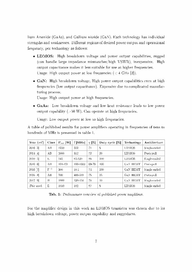
A table of published results for power ampliers operating in frequencies of tens to
hundreds of MHz is presented in table 1.
Year (ref) Class Pout [W] f [MHz] η [%] Duty cycle [%] Technology Architecture
2016 [3] AB 1250 352 71 5 LDMOS Single-ended
2014 [4] AB 2000 352 72 20 LDMOS Push-pull
2010 [5] E 145 85-120 86 100 LDMOS Single-ended
2010 [6] AB 104-121 100-1000 69-79 100 GaN HEMT Push-pull
2016 [7] F−1 300 10.1 74 100 GaN HEMT Single-ended
2016 [8] AB 700 400-500 75 15 GaN HEMT Push-pull
2017 [9] B 1000 420-450 70 10 GaN HEMT Single-ended
This work E 1050 102 87 5 LDMOS Single-ended
Tab. 1: Performance overview of published power ampliers.
For the amplier design in this work an LDMOS transistor was chosen due to its
high breakdown voltage, power output capability and ruggedness.
7

3 Theory
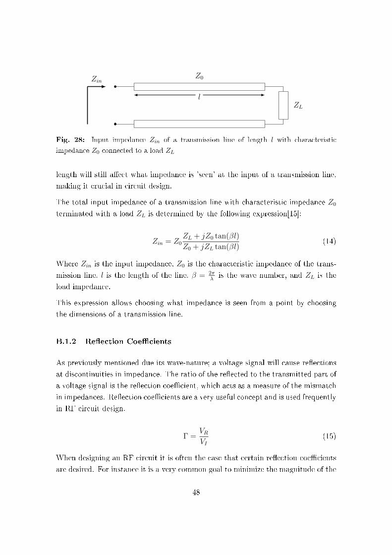
This section will assume that the reader is familiar with some concepts of microwave
engineering such as: Transmission lines, reection coecients, the Smith-chart,
impedance matching, and scattering parameters. For a brief overview of these sub-
jects, see appendix B.
3.1 RF power ampliers
An RF power amplier can be seen as consisting of a few distinct parts. Namely,
The input matching network, the transistor, the output matching network and the
bias network. A diagram of the basic structure of a power amplier is presented in
g 1:
Fig. 1: Schematic diagram of an RF power amplier.
The reection coecients of the transistor input and output are denoted Γin and
Γout, and the coecients for the source and load are denoted ΓS and ΓL respectively.
The source and load are typically 50 Ohms which is generally not the same as
the input and output impedance of the transistor. Therefore we utilize matching
networks on the input and output to match the impedances of the source and load
to the desired impedances (i.e. reection coecients) at the input and output of the
transistor.
8

The DC-bias networks supply the amplier with DC power that is to be converted
to RF output power. It also provides the biasing conditions to allow the transistor
to operate with the desired gate-source voltage.
The eciency of the amplier is the ratio between output RF power and the supplied
DC power:
η =PoutPDC
(1)
Though, there are numerous dierent measures of eciency, and another commonly
used measure is the power added eciency which takes into account the RF power
supplied to the amplier.
PAE =Pout − PinPDC
(2)
The power added eciency is often a more suitable measure of an ampliers e-
ciency, since neglecting the input power is rarely useful. This is especially true at
lower gains, where the eects of neglecting input power are more signicant.
3.2 Stability
The stability of an amplier describes its resilience towards self induced oscillations.
These oscillations can occur if a voltage seen at the output induces a voltage at the
input. This type of feedback behavior gets amplied due to the voltage gain of the
amplier and causes unwanted oscillations.
An amplier can be either conditionally or unconditionally stable. An uncondition-
ally stable amplier will remain stable regardless of what impedance it sees on the
source and load.
A conditionally stable amplier will only be stable for a subset of source and load
impedances.
The stability of an amplier can be determined analytically using S-parameter val-
ues. The s-parameters of the amplier can be used to calculate two measures of
stability K and ∆
9

An amplier is unconditionally stable if both K > 1 and |∆| < 1.
Where K and |∆| are described by the following equations[15]:
K =1− |S11|2 − |S22|2 + |∆|2
2|S21S12|(3)
Where the ∆ is described by:
∆ = S11S22 − S12S21 (4)
Since the S-parameters of an amplier is frequency dependent, so is the measures
of stability. That is to say an amplier may be unconditionally stable for some
frequencies and simultaneously be conditionally stable for others.
3.3 Classes of operation
Ampliers are generally classied according to which class of operation the transistor
is operating in. The classes of operation can be divided into transconductance classes
and Switch-mode classes.
The transconductance classes, A, AB, B and C are classied according to their
conduction angle. The conduction angle of an amplier is the part of a gate volt-
age signal for which the transistor is conducting, and is determined by the biasing
conditions of the transistor.
A Class A power amplier is biased to conduct for the entire period of the input
signal. And thus has a conduction angle of 360 Since it is always conducting,
there is current constantly owing through the device resulting in signicant
losses. It has a theoretical maximum eciency is 50% [16].
A Class B amplier is biased so that it is balancing on the threshold voltage,
any positive voltage on the input will cause conduction and as such it has a
conduction angle of 180. It has a theoretical maximum eciency is 78.5%
[16].
A Class AB amplier is biased somewhere in between class A and class B
and consequently has a conduction angle between 180 and 360. And it has
10

theoretical eciencies between 50% and 78.5%
A class C amplier is biased so that the conduction angle is less than 180
Smaller conduction angle gives less quiescent current losses. It is capable of
higher theoretical eciency than class B but suers from lower gain.
Switch-mode classes like class D and E are not really dened by their biasing. Instead
the transistor is operated like a switch that jumps back and forth between cuto
and saturation. Ideally switch-mode ampliers are driven using input voltage to
facilitate fast switching.
The main advantage of switch mode classes is that the transistor is either entirely
conducting or entirely non-conducting. This ensures low losses since it leads to no
simultaneous voltage and current in the device. Since while the transistor is on there
is a large current but low a voltage, and when the transistor is o there is a high
voltage but a low current in the device [16].
3.3.1 Biasing and conduction angles
For practical reasons it one might choose to not use a square wave voltage at the
input for a switch mode amplier. When using a square wave input signal the
conduction angle is just the duty cycle of the square wave signal.
If we instead assume a sinusoidal voltage and we wish to achieve a certain conduction
angle, a DC-oset can be applied to the signal.
Assume that conduction occurs for all positive voltages and that the input signal is
on the following form:
Vin = A · sin(ωt)
If a DC-bias A · ε is added, the signal becomes:
Vinε = A · (sin(ωt) + ε)
The relationship between added DC bias and conduction angle is illustrated in gure
2 . Three voltage signals are plotted for the cases of positive, zero, and negative
DC-bias.
11

Fig. 2: Sinusiodal voltage signals, each with a dierent DC-bias Aε. The conducting part
of each signal is shaded.
The problem of when an ideal voltage switch is conducting for a DC-oset sinu-
soidal input voltage can be reformulated into the geometrical problem of nding a
relationship between θCA and ε in the image below:
0V
Aε V
θCA
α αε
It can be seen that:
ε = sin(α) =⇒ α = arcsin(ε)
The angle α is readily expressed in terms of the conduction angle:
α =θCA − π
2
This gives the following relationship between ε and θCA:
π + 2 arcsin(ε) = θCA
12

3.4 Class E
As a switch mode amplier, the objective of a class E amplier is to separate voltage
and current in the transistor. This is the main idea behind using the transistor as
a switch. While the switch is closed, the current ows through the switch, but it
has no resistance and therefore there is no voltage drop over the switch. While
the switch is open there is a voltage drop over the switch but there is no current
owing. Losses in the transistor occur only when voltage and current waveforms
overlap, since the power dissipated is the product of the voltage and current in the
device [19].
A schematic of an ideal class E amplier can be seen in gure 3.
V+
V−
Shunt capacitor
Tuning inductor
DC power supply
Voltage source
Load
Voltage-controlled switch
Resonator
I0 sin (ωrest)
ΓL
Fig. 3: Schematic diagram of an ideal class E circuit.
An ideal class E amplier can be divided into a few basic parts which have been
labeled in the above image. The circuit consist of a voltage controlled switch which
is turned ON and OFF by a voltage source at the input. The output side of the
switch is connected to a DC-power supply, and to the output circuit, which in turn
is connected to the load.
The output circuit consists of three parts:
The resonator consisting of a inductor and a capacitor. It acts as a band pass
lter, which transmits the resonant frequency but lters out harmonics.
The shunt capacitor which allows current to be drawn from ground while the
switch is open.
13
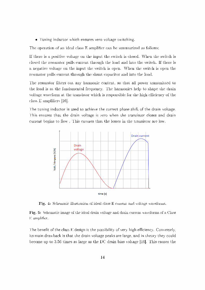
Tuning inductor which ensures zero voltage switching.
The operation of an ideal class E amplier can be summarized as follows:
If there is a positive voltage on the input the switch is closed. When the switch is
closed the resonator pulls current through the load and into the switch. If there is
a negative voltage on the input the switch is open. When the switch is open the
resonator pulls current through the shunt capacitor and into the load.
The resonator lters out any harmonic content, so that all power transmitted to
the load is at the fundamental frequency. The harmonics help to shape the drain
voltage waveform at the transistor which is responsible for the high eciency of the
class E ampliers [16].
The tuning inductor is used to achieve the correct phase shift of the drain voltage.
This ensures that the drain voltage is zero when the transistor closes and drain
current begins to ow . This ensures that the losses in the transistor are low.
Fig. 4: Schematic illustration of ideal class E current and voltage waveforms.
Fig. 5: Schematic image of the ideal drain voltage and drain current waveforms of a Class
E amplier.
The benet of the class E design is the possibility of very high eciency. Conversely,
its main drawback is that the drain voltage peaks are large, and in theory they could
become up to 3.56 times as large as the DC drain bias voltage [16]. This causes the
14

breakdown voltage of the transistor to become a limiting factor when designing class
E ampliers.
The set of equations that relate the operation of an amplier to its components
is known as its design equations. The design equations for class E ampliers were
reported by N. Sokal in 1975 [10]. Some examples of the equations are presented
below:
Rload =(Vcc − VTh)2
Pout(5)
Cshunt =1
ωRload · 5.447(6)
Ltune =1.1525 ·Rload
ω(7)
However, these equations assume a 50% duty cycle, and it is not necessarily the
duty cycle that will ensure optimal performance in any given design.
Equations that take duty cycle into account were published by Raab in 1977 [11].
However they are cumbersome and usually used in graphical a format or computer
templates rather than in explicit form.
15
4 Design and Simulation
The measurement equations used in the ADS simulations are displayed in
Appendix A
4.1 The transistor: Ampleon BLF188XR
The transistor used for the amplier is an LDMOS power transistor from Ampleon
named BLF188XR [13]. In each unit casing there are two transistors. Each transistor
has a maximum drain source current of 77 amperes and a maximum drain source
voltage of 135 volts. The choice of this transistor is due to it having high gain and
tolerating high voltage peaks and currents without degradation.
4.2 Frequency of operation
The choice of operational frequency was the highest possible from a set of frequencies
of interest, considering the transistor. The frequencies all relating to application in
particle accelerators.
Initially, simulations of class E ampliers were made for the frequencies 352 MHz
and 704 MHz but did not yield functioning circuits.
The reason for this is that the output capacitance of the transistor (212 pF) limits
the maximum operating frequency.
The maximum operating frequency of an optimal class E amplier is given by the
expression [16]:
fmaxE =Imax
56.5CoutVcc≈ 130 MHz
Above this frequency-threshold eciency will start to suer since the drain voltage
waveform is limited by the charging of the output capacitance.
Using the maximum values for our transistor we get a theoretical frequency limit of
approximately 130 MHz. This conrmed the decision to realize a 100 MHz amplier.
16
This maximum frequency of class E operation should not be confused with the
frequency of unity gain for the transistor, commonly denoted fmax. which is higher.
For the BLF188XR the frequency of unity gain was found to be about 700 MHz in
simulation with Vgs =2 V and Vds = 45 V.
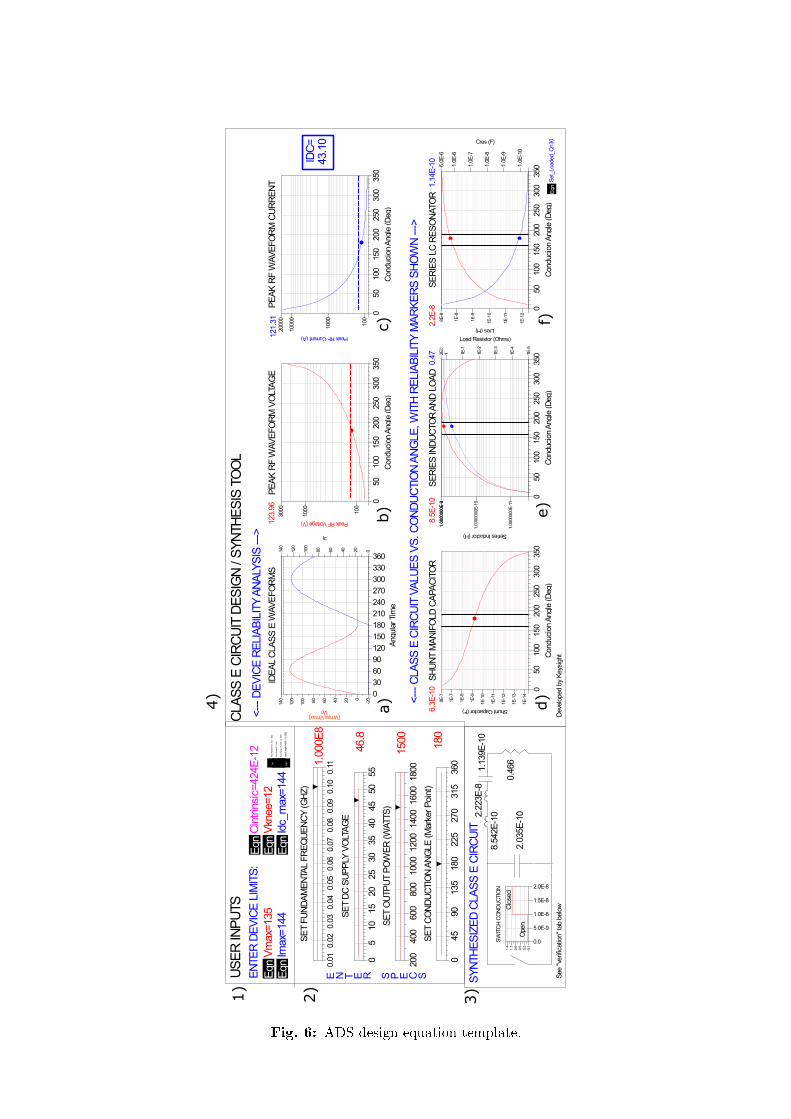
4.3 Lumped component circuit
The amplier is designed using the class E design equations from Raab [11], which
result in a circuit composed of lumped components.
A template that implements the design equations in ADS was used [18]. The design
equation template is displayed in gure 6.
The subsections of the template have been numbered, their functions are:
1. Allows the user to enter the following device parameters and limits:
Vmax - The maximum allowed drain voltage peaks.
Imax - The maximum allowed drain current peaks.
Cintrinsic - The output capacitance of the transistor (CDS).
Vknee - The knee voltage of the transistor. (Found from DC-simulation).
IDC−max - Maximum allowed DC drain current.
2. Allows the user to choose the following circuit parameters:
Frequency of operation.
DC-supply voltage (Drain bias).
Output power.
Conduction angle (θCA).
3. Displays the component values of the synthesized circuit.
17

4. Displays waveforms, peak drain voltage and -current values, and circuit values.
(a) Displays the drain voltage and -current waveforms of the synthesized
circuit.
(b) Displays the peak value of drain voltage as a function of conduction an-
gle. Higher conduction angles leads to higher drain voltage peaks, so the
maximum allowed drain voltage sets an upper bound for θCA.
(c) Displays the peak value of drain current as a function of θCA. Lower
θCA leads to higher drain current peaks, so the maximum allowed drain
current sets a lower bound for θCA.
(d) Displays the shunt capacitance value a function of θCA The bounds on
θCA mark the range of shunt capacitance values that produce a reliable
circuit.
(e) Displays the values of the tuning inductor and the load resistance as
a function of θCA. The bounds on θCA mark the range of values that
produce a realiable circuit.
(f) Displays the values of the resonator capacitance and inductance as a func-
tion of θCA. The bounds on θCA mark the range of values that produce
a reliable circuit.
A single ended design was constructed in ADS using a simulation model of the
BLF188XR transistor and lumped components calculated from the design equations.
The ADS simulation setup for the lumped component circuit can be seen in gure
7.
18
1.14
E-1
0
0.46
6
1.13
9E-1
02.
223E
-8
180
1500
1.00
0E8
46.8
8.5E
-10
0.47
6.3E
-10
123.
96
2.03
5E-1
0
5010
015
020
025
030
00
350
1E-1
3
1E-1
2
1E-1
1
1E-1
0
1E-9
1E-8
1E-7
1E-1
4
9E-7
Con
duci
on A
ngle
(Deg
)
Shunt Capacitor (F)
SH
UN
T M
AN
IFO
LD C
APA
CIT
OR
5010
015
020
025
030
00
350
1.00
0000
0E-1
0
1.00
0000
0E-9
1.00
0000
0E-1
1
1.00
0000
0E-9
1E-4
1E-3
1E-2
1E-1
1 1E-5
2E0
Con
duci
on A
ngle
(Deg
)
Series Inductor (H)
Load Resistor (Ohms)
SE
RIE
S IN
DU
CTO
R A
ND
LO
AD
5010
015
020
025
030
00
350
1E-1
1
1E-1
0
1E-9
1E-8
1E-1
2
8E-8
1.0E
-9
1.0E
-8
1.0E
-7
1.0E
-6
1.0E
-10
6.0E
-6
Con
duci
on A
ngle
(Deg
)
Lres (H)
Cres (F)
SE
RIE
S L
C R
ES
ON
ATO
R
5010
015
020
025
030
00
350
1000 100
3000
Con
duci
on A
ngle
(Deg
)
Peak RF Voltage (V)
PE
AK
RF
WAV
EFO
RM
VO
LTA
GE
Eqn
Vm
ax=1
35E
qnIm
ax=1
44
4590
135
180
225
270
315
036
0
SE
T C
ON
DU
CTI
ON
AN
GLE
(Mar
ker P
oint
)
Clo
sed
5.0E-9
1.0E-8
1.5E-8
0.0
2.0E-8
0.2
0.5
0.8
1.1
-0.11.4
SW
ITC
H C
ON
DU
CTI
ON
Ope
n
30
60
90
120
150
180
210
240
270
300
330
0
360
020406080100
120
-20
140
20406080100
120
0140
Ang
ular
Tim
e
Vc
Ic
[Vmax,Vmax]
IDE
AL
CLA
SS
EW
AVE
FOR
MS
Eqn
Vkn
ee=1
2E
qnV
cc_R
ange
=[1:
:.2::5
0]
510
1520
2530
3540
4550
055
SE
T D
C S
UP
PLY
VO
LTA
GE
Eqn
Freq
_Ran
ge=[
1e7:
:.1e6
::1.1
e8]
0.02
0.03
0.04
0.05
0.06
0.07
0.08
0.09
0.10
0.01
0.11
SE
T FU
ND
AM
EN
TAL
FRE
QU
EN
CY
(GH
Z)
Eqn
Pou
t_R
ange
_W=[
200:
:10:
:180
0]
400
600
800
1000
1200
1400
1600
200
1800
SE
T O
UTP
UT
PO
WE
R (W
ATTS
)
8.54
2E-1
0
2.2E
-8
Eqn
Cin
trins
ic=4
24E
-12
<---
DE
VIC
E R
ELI
AB
ILIT
Y A
NA
LYS
IS --
->
<---
CLA
SS
E C
IRC
UIT
VA
LUE
S V
S. C
ON
DU
CTI
ON
AN
GLE
, WIT
H R
ELI
AB
ILIT
Y M
AR
KE
RS
SH
OW
N --
->
Eqn
Set
_Loa
ded_
Q=3
0
SY
NTH
ES
IZE
D C
LAS
S E
CIR
CU
IT
US
ER
INP
UTS
Eqn
Idc_
max
=144
43.1
0ID
C=
121.
31
5010
015
020
025
030
00
350
1000
1000
0
100
2000
0
Con
duci
on A
ngle
(Deg
)
Peak RF Current (A)
PE
AK
RF
WAV
EFO
RM
CU
RR
EN
T
See
"ve
rific
atio
n" ta
b be
low
CLA
SS
E C
IRC
UIT
DE
SIG
N /
SY
NTH
ES
IS T
OO
LE
NTE
R D
EV
ICE
LIM
ITS
:
E N T E R S P E C S
Dev
elop
ed b
y K
eysi
ght
Eqn
cond
_ang
le1=
[10:
:10:
:350
]
1)
2)
3)
4)
a)b)
c)
d)
e)f)
Fig. 6: ADS design equation template.

STA TB
A B
Var
Eqn
Var
Eqn
Var
Eqn
HA
RM
ON
IC B
ALA
NC
E
Mea
sE
qn
Mea
sE
qn
Mea
sE
qnMea
sE
qn
Mea
sE
qn
OP
TIM
GO
AL
GO
AL
GO
AL
Goa
l Goa
l
Goa
l
Opt
imM
easE
qn
Mea
sEqn
Mea
sEqn
Mea
sEqn
Mea
sEqn
V_1
Tone
I_P
robe
V_D
CD
C_F
eed
Har
mon
icB
alan
ce
C
I_P
robe
I_P
robe
R
SLC
L
I_P
robe
VA
RV
AR
VA
R
V_D
CD
C_F
eed
I_P
robe
AM
P_B
LF18
8XR
_V1p
02
Opt
imG
oal4
Opt
imG
oal3
Opt
imG
oal2
Opt
im2
Mea
s9
Mea
s8
Mea
s7
Mea
s5
Mea
s6
SR
C5
SR
C3
DC
_Fee
d2
HB
1
C1
iout
ic
Rou
t
SLC
1L1
Circ
uit_
para
met
ers
Inpu
tV
SR
C2
DC
_Fee
d1
ids
idc
iin
LDM
N1
Wei
ght=
1S
imIn
stan
ceN
ame=
"HB
1"E
xpr=
"pou
t"
Wei
ght=
1S
imIn
stan
ceN
ame=
"HB
1"E
xpr=
"vm
ax"
Wei
ght=
1S
imIn
stan
ceN
ame=
"HB
1"E
xpr=
"PA
E"
Sav
eAllT
rials
=no
Ena
bleC
ockp
it=ye
sS
aveC
urre
ntE
F=
no
Use
AllG
oals
=ye
sU
seA
llOpt
Var
s=ye
sS
aveA
llIte
ratio
ns=
noS
aveN
omin
al=
noU
pdat
eDat
aset
=ye
sS
aveO
ptim
Var
s=no
Sav
eGoa
ls=
yes
Sav
eSol
ns=
yes
Set
Bes
tVal
ues=
yes
Nor
mal
izeG
oals
=ye
sF
inal
Ana
lysi
s="N
one"
Sta
tusL
evel
=4
Des
iredE
rror
=0.
0M
axIte
rs=
100
Opt
imTy
pe=
Gra
dien
tpd
c =
vcc
mea
s[0]
*idc
.i[0]
pout
= r
eal(0
.5*v
out[1
]*co
nj(io
ut.i[
1]))
PA
E =
100
*rea
l((po
ut-p
in)/
pdc)
pin
= r
eal(0
.5*v
in[1
]*co
nj(ii
n.i[1
]))
vmax
= m
ax(t
s(vd
s))
Fre
q=10
0 M
Hz
V=
pola
r(vp
,0)
V
vgs=
3.97
208
o
vp=
12.3
14
o
Vdc
=vg
s
Ord
er[1
]=20
Fre
q[1]
=10
0 M
Hz
C=
Csh
R=
R
C=
Co
L=Lo
R=
L=L
R=
0.64
3497
o
Lo=
2.91
4e-8
L=1.
0230
9e-0
09
oC
o=8.
692e
-11
Csh
=1.
7555
3e-0
10
ofr
eque
ncy=
100e
6vc
c=44
.765
7 o
Vdc
=vc
c
vccm
eas
vin
vds
vout
Fig. 7: Simulation setup for the lumped component circuit.
The design equations provide a good starting point for the circuit, but they assume
a perfect voltage switch as a transistor and as such the circuit needs to be tuned to
accommodate the dierences that arise from using a more realistic transistor model.
Once lumped circuit component values have been found that give satisfactory per-
formance, the impedance seen at the output of the transistor is determined. The
output impedance is used as a target for constructing the circuit using transmission
lines.
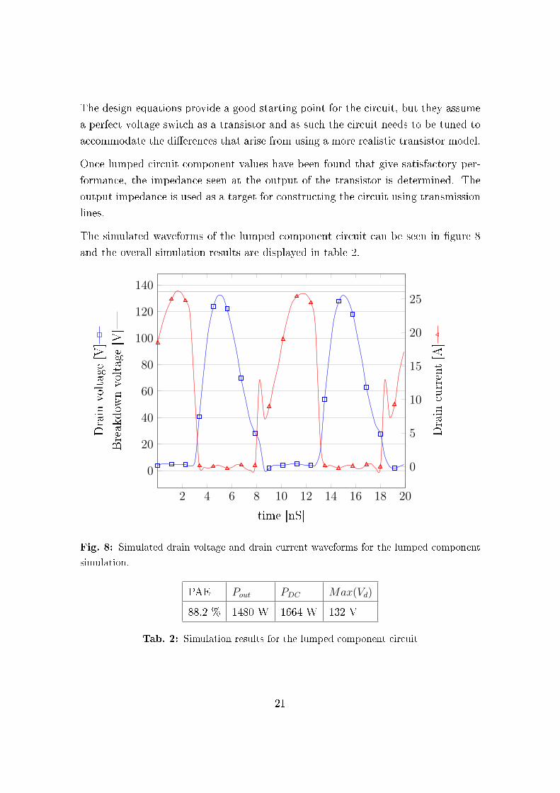
The simulated waveforms of the lumped component circuit can be seen in gure 8
and the overall simulation results are displayed in table 2.
2 4 6 8 10 12 14 16 18 20
0
20
40
60
80
100
120
140
0
5
10
15
20
25
time [nS]
Drain
voltage[V]
Breakdow
nvoltage[V]
Drain
current[A]
Fig. 8: Simulated drain voltage and drain current waveforms for the lumped component
simulation.
PAE Pout PDC Max(Vd)
88.2 % 1480 W 1664 W 132 V
Tab. 2: Simulation results for the lumped component circuit
21
4.4 Design using transmission lines
After the impedance using lumped components is established, a design using ideal
transmission lines can be devised. The aim is now to construct the target impedance
using only transmission lines and shunt capacitors.
The circuit is designed by matching the target impedance at the output to the 50Ω
impedance of the load. To achieve this matching a Smith chart was used. The
matching is performed adding transmission lines and shunt capacitors as a way to
move in the Smith chart.
Once the circuit is constructed component values could be tuned to further improve
the performance.
Once a circuit using ideal transmission lines has been produced the next step is
to perform simulations using more realistic transmission lines; since eects such as
losses and the inuence of a substrate needs to be considered.
The tool 'MLIN' in ADS allows for the simulation of microstrip lines including choice
of substrate parameters.
To achieve the desired performance the circuit values are optimized using the opti-
mization tool in ADS.
The optimization tool in ADS allows the user to automatically optimize the perfor-
mance of a circuit using a set of user dened optimization goals. The tool attempts
to iteratively nd a solution based on the optimization goals by sweeping chosen
variables incrementally, such as component values.
The transmission line circuit was optimized by varying the dimensions of the trans-
mission lines, the values of shunt and DC-block capacitors, gate and drain biases,
input power and RF choke inductors.
Using goals of 1500 W output power, 90% power added eciency and shunt capacitor
voltages below 500 V. All of the goals will not realistically be reached, but are chosen
to push the solution in a desired direction. The goals were chosen to prioritize power
added eciency.
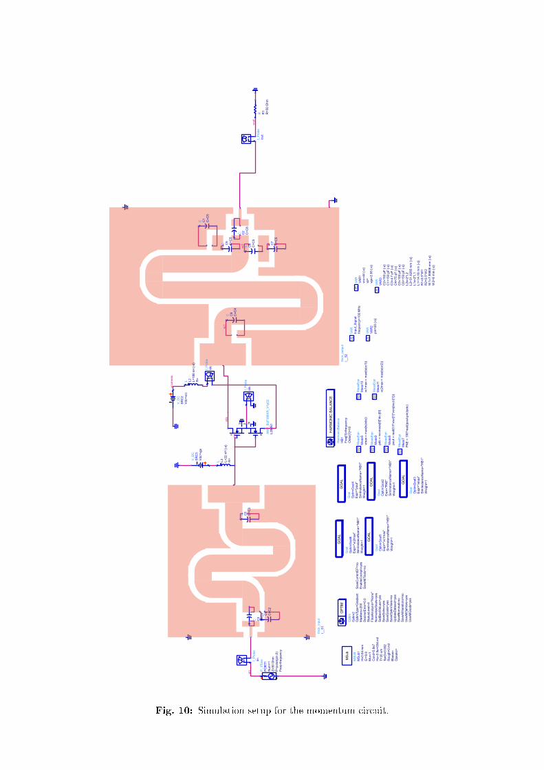
The resulting simulated circuit can be seen in image 9. The full input and output
matching networks are not included in the image since they are way too big.
22

STA TB
A B
Var
Eqn
Var
Eqn
HA
RM
ON
IC B
ALA
NC
E
Mea
sE
qn
Mea
sE
qn
Mea
sE
qn
Mea
sE
qn
GO
AL
OP
TIM
GO
AL
GO
AL
Var
Eqn
GO
AL
Mea
sE
qn
Mea
sE
qn
GO
AL
MS
ub
Var
Eqn
vc1
vin
vccm
eas
vds
MLI
N
L
MLI
N
VA
R
L
C
MTE
E_A
DS
MTE
E_A
DS
MLI
NM
SU
B
MLI
N
Goa
l
Mea
sEqn
Mea
sEqn
VA
R
Opt
im
Goa
lG
oal
Goa
lG
oal
Mea
sEqn
Mea
sEqn
Mea
sEqn
Mea
sEqn
V_D
C
Har
mon
icB
alan
ce
C
VA
R
VA
R
V_D
C
I_P
robe
AM
P_B
LF18
8XR
_V1p
02
I_P
robe
L2
TL38
L1
Tee2
C5
TL20
C6
Tee4
TL15
MS
ub1
TL23
Opt
imG
oal6
Mea
s10
Mea
s11
VA
R2
Opt
im2
Opt
imG
oal5
Opt
imG
oal4
Opt
imG
oal3
Opt
imG
oal2
Mea
s9
Mea
s8
Mea
s7
Mea
s6
SR
C3
HB
1
idc
Inpu
t_S
igna
l
VA
R1
SR
C2
ids
LDM
N1
VA
R3
L2x=
2*L2
C6=
112.
71 p
F
o
L2=
31.9
336
mm
o
L1x=
2*L1
C5=
88.0
552
pF
oC
4=86
.645
5 pF
o
C3=
5.03
622
pF
oC
1=12
6.54
8 pF
o
L=1
mm
W=
W2
Sub
st=
"MS
ub1"
W2=
8 m
m
o
C=
C3
W1=
7.83
973
mm
o
L=18
nH
L=13
.034
6 m
m
o
C2=
110.
871
pF
o
C=
C4
W=
23.6
935
mm
o
Sub
st=
"MS
ub1"
R=
W2=
W1
W3=
12.2
837
mm
o
W1=
W1
Sub
st=
"MS
ub1"
W=
24.0
702
mm
o
Sub
st=
"MS
ub1"
Dpe
aks=
Bba
se=
Rou
gh=
0 m
ilTa
nD=
0.00
2T=
35 u
mH
u=3.
9e+
034
mil
Con
d=5.
8e7
Mur
=1
Er=
9.8
H=
0.64
mm
W=
W1
Sub
st=
"MS
ub1"
Sub
st=
"MS
ub1"
R1=
0.5*
W1
R2=
0.5*
W2
Exp
r="v
c2m
ax"
Sim
Inst
ance
Nam
e="H
B1"
vc1m
ax =
max
(ts(
vc1)
)
Ena
bleC
ockp
it=ye
sS
aveA
llTria
ls=
no
Sav
eCur
rent
EF
=no
Use
AllG
oals
=ye
sU
seA
llOpt
Var
s=ye
s
vc2m
ax =
max
(ts(
vc2)
)
pin=
14.9
916
o
Sav
eGoa
ls=
yes
Sav
eOpt
imV
ars=
noU
pdat
eDat
aset
=ye
sS
aveN
omin
al=
noS
aveA
llIte
ratio
ns=
no
Sta
tusL
evel
=4
Fin
alA
naly
sis=
"Non
e"N
orm
aliz
eGoa
ls=
yes
Set
Bes
tVal
ues=
yes
Sav
eSol
ns=
yes
Opt
imTy
pe=
Gra
dien
tM
axIte
rs=
200
Des
iredE
rror
=0.
0
Exp
r="v
c1m
ax"
Sim
Inst
ance
Nam
e="H
B1"
Wei
ght=
1
Exp
r="p
out"
Sim
Inst
ance
Nam
e="H
B1"
Wei
ght=
1
Exp
r="v
max
"S
imIn
stan
ceN
ame=
"HB
1"W
eigh
t=1
Exp
r="P
AE
"S
imIn
stan
ceN
ame=
"HB
1"W
eigh
t=1
pdc
= v
ccm
eas[
0]*i
dc.i[
0]
pout
= r
eal(0
.5*v
out[1
]*co
nj(io
ut.i[
1]))
PA
E =
100
*rea
l((po
ut-p
in)/
pdc)
vmax
= m
ax(t
s(vd
s))
L=8.
0491
4 m
m
o
Vdc
=vg
s
Ord
er[1
]=20
Fre
q[1]
=10
0 M
Hz
L=2
mm
L=18
nH
L1=
13.3
854
mm
o
Wei
ght=
1
freq
uenc
y=10
0e6
vgs=
2.29
756
o
vp=
vcc=
46.0
425
o
Vdc
=vc
c
W3=
8.78
314
mm
o
W2=
W2
R=
W1=
W2
Fig. 9: Simulation setup for the microstrip circuit.

After the optimization of the realistic transmission lines the results in table 3 were
found.
PAE Pout PDC Max(Vds) Max(VC1) Max(VC2)
83.2 % 1415 W 1702 W 131 V 128 V 460 V
Tab. 3: Simulation results for the microstrip circuit.
Compared to simulations using ideal lumped components the eciency of the simu-
lated amplier has decreased, which is to be expected since the microstrip simulation
takes into account losses in the transmission lines.
4.5 Momentum simulations
The electromagnetic elds produced during operation of the amplier give rise to
eects that could aect its performance. For instance there could be capacitive
coupling between the transmission lines and the surrounding ground plane of the
amplier.
In order to take these eects into consideration the electromagnetic elds of the
operating amplier needs to be simulated in beforehand.
To simulate the electromagnetic elds a complete model of the amplier needs to be
constructed including the type and dimensions of the substrate, the copper thickness,
ground planes, etc.
The momentum simulator uses numerical computational methods to solve the par-
tial dierential equations that describe electromagnetic eld, which are Maxwell's
equations.
After the momentum simulation circuit has been optimized to achieve ideal perfor-
mance the simulation part of the design process is complete.
Figure 10 depicts the momentum simulation circuit in ADS, table 4 shows the simu-
lation results, and gure 11 displays the simulated drain current and -voltage wave-
forms.
24
STA TB
A B
Var
Eqn
Var
EqnVar
Eqn
Var
Eqn
MS
ub
HA
RM
ON
IC B
ALA
NC
E Mea
sE
qn
Mea
sE
qn
Mea
sE
qn
Mea
sE
qn
Mea
sE
qnMea
sE
qn
GO
AL
GO
AL
GO
AL
GO
AL
GO
AL
OP
TIM
vc1
vc2
vds
vccm
eas
vout
vin
vin
Opt
im
Goa
l
Goa
l
Goa
l
Goa
l Goa
l
Mea
sEqn
Mea
sEqn
Mea
sEqn
Mea
sEqn
Mea
sEqn
Mea
sEqn
P_1
Tone
Har
mon
icB
alan
ce
MS
UB
L
VA
R
VA
R
VA
R
VA
R
V_D
C
V_D
C
C
C
C
CC
C
C
C
C
I_P
robe
I_P
robe
I_P
robe
I_P
robe
R
AM
P_B
LF18
8XR
_V1p
02
L
thic
k_in
put
thic
k_ou
tput
Opt
im2
Opt
imG
oal2
Opt
imG
oal6
Opt
imG
oal5
Opt
imG
oal4
Opt
imG
oal3
Mea
s6
Mea
s7
Mea
s8
Mea
s9
Mea
s10
Mea
s11
L3
PO
RT1
HB
1
MS
ub1
L2
VA
R1
Inpu
t_S
igna
l
VA
R2
VA
R3
SR
C2
SR
C3
C9
C6
C3
C2
C5
C8 C
7
C1
C4
ids
idc
iinio
utR
1
LDM
N1
I__5
2
I__5
1
Sav
eAllT
rials
=no
Ena
bleC
ockp
it=ye
sS
aveC
urre
ntE
F=
no
Use
AllG
oals
=ye
sU
seA
llOpt
Var
s=ye
sS
aveA
llIte
ratio
ns=
noS
aveN
omin
al=
noU
pdat
eDat
aset
=ye
sS
aveO
ptim
Var
s=no
Sav
eGoa
ls=
yes
Sav
eSol
ns=
yes
Set
Bes
tVal
ues=
yes
Nor
mal
izeG
oals
=ye
sF
inal
Ana
lysi
s="N
one"
Sta
tusL
evel
=4
Des
iredE
rror
=0.
0M
axIte
rs=
200
Opt
imTy
pe=
Gra
dien
t
Wei
ght=
1S
imIn
stan
ceN
ame=
"HB
1"E
xpr=
"PA
E"
Wei
ght=
1S
imIn
stan
ceN
ame=
"HB
1"E
xpr=
"vc2
max
"
Wei
ght=
1S
imIn
stan
ceN
ame=
"HB
1"E
xpr=
"vc1
max
"
Wei
ght=
1S
imIn
stan
ceN
ame=
"HB
1"E
xpr=
"pou
t"
Wei
ght=
1S
imIn
stan
ceN
ame=
"HB
1"E
xpr=
"vm
ax"
vmax
= m
ax(t
s(vd
s))
PA
E =
100
*rea
l((po
ut-p
in)/
pdc)
pout
= r
eal(0
.5*v
out[1
]*co
nj(io
ut.i[
1]))
pdc
= v
ccm
eas[
0]*i
dc.i[
0]
vc1m
ax =
max
(ts(
vc1)
)
vc2m
ax =
max
(ts(
vc2)
)
R=
L=22
nH
-o
Fre
q=fr
eque
ncy
P=
pola
r(pi
n,0)
Z=
50 O
hmN
um=
1
Ord
er[1
]=10
Fre
q[1]
=fr
eque
ncy
Dpe
aks=
Bba
se=
Rou
gh=
0 m
ilTa
nD=
0.00
2T=
35 u
mH
u=3.
9e+
034
mil
Con
d=5.
8e7
Mur
=1
Er=
9.8
H=
0.64
mm
R=
L=18
8 nH
-o
vcc=
44
-o
vp=
vgs=
2.55
-o
freq
uenc
y=10
0 M
Hz
pin=
20
-o
C2=
150
pF
-o
C1=
150
pF
-o
C3=
4.7
pF
-o
C4=
75 p
F
-o
C5=
100
pF
-o
C6=
150
pF
-o
L2x=
2*L2
L2=
31.8
285
mm
-o
L1
x=2*
L1L1
=14
.16
mm
-o
R
1=0.
5*W
1R
2=0.
5*W
2W
1=7.
9980
6 m
m
-o
W2=
8 m
m
-o
Vdc
=vc
c
Vdc
=vg
s
C=
C5
C=
C4
C=
C1
C=
C6
C=
C3
C=
C5
C=
C5
C=
C5
C=
C2
R=
50 O
hm
Fig. 10: Simulation setup for the momentum circuit.

2 4 6 8 10 12 14 16 18 20
0
20
40
60
80
100
120
140
0
5
10
15
20
time [nS]
Drain
voltage[V]
Breakdow
nvoltage[V]
Drain
current[A]
Fig. 11: Simulated drain voltage and drain current waveforms for the momentum simu-
lation.
PAE Pout PDC Max(Vds) Max(VC1) Max(VC2)
75.8 % 1330 W 1730 W 131 V 105 V 417 V
Tab. 4: Simulation results for the momentum circuit.
26

4.6 Stability analysis
To determine the conditions of stability of the transistor a stability simulation was
performed. A stability simulation consists of simulating the S-parameters of an am-
plier circuit over a range of frequencies and calculating the the stability parameters
K and |∆| at each frequency.
20 40 60 80 100 120 140 160 180 2000
0.5
1
1.5
2
2.5
Frequency [MHz]
K |∆|
Fig. 12: Simulated stability parameters for the MLIN simulation circuit.
From the stability simulation in gure 12 we can see that both conditions for un-
conditional stability are fullled at the design frequency of 100 MHz. The transistor
will be conditionally stable at frequencies of 15 MHz or lower since the stability
factor K drops below 1.
A way of ensuring unconditional stability below 15 MHz is to add a resistor to
ground at the transistor input [12]. This was however overlooked at the time of
circuit design.
27
5 Amplier construction
The circuit board used for the amplier was produced by hand using an etching
method. From the momentum simulation a prole of the circuit was acquired. By
printing this prole on photo-paper and laminating it to the circuit board, the ink
is transferred to the circuit board. The entire circuit board is then submerged in
the etching solution and the copper that is not covered by the ink mask is etched
away.
The substrate used to create the circuit board is a 0.64 mm double-sided copper
clad Rogers TMM10i. It was chosen primarily for its high electrical permitivity, but
also for its tolerance to heating [20].
Property: Typical value:
Dielectric constant, εr 9.8 ± 0.245
Dissipation factor, tan(δ) 0.0020
Dielectric thickness 0.635 mm
Copper thickness 35µm
Tab. 5: Table of substrate parameters for Rogers TMM10i.
The high electrical permitivity ensures that the circuit can remain relatively small.
Considering that at 100 MHz transmission lines tend to be quite large.
The substrate has copper layers on both sides with thicknesses of 35 µm. The
bottom layer is left unectched and serves as a ground plane.
The circuit is designed to have ground planes on the top layer, surrounding the
transmission lines. In order to create a connection between the bottom and top
ground planes; 1 mm diameter holes were drilled through the PCB and conductors
were soldered through the holes on both sides of the PCB. This process is known as
viasing and is a common technique for connecting two sides of a PCB.
After the viasing was performed the bottom side of the PCB was covered in solder
to ensure a good connection between the viasing and the ground plane. The solder
was then sanded at in order to allow the circuit board to lie ush against the heat
sink.
28

Once the circuit board was prepared, the lumped components for the amplier such
as capacitors, inductors and the transistor could be soldered by hand.
The circuit design allows for moving capacitors along the transmission lines for
future tuning.
The capacitors used are Cornell Dublier mica capacitors with a rated maximum
voltage of 300 volts. However, the simulated voltage drop over the second output
capacitor is about 420 volts.
To solve this issue the second output capacitance is produced with the use of 4
capacitors, namely two serially connected pairs of parallel capacitors. This setup
has the same capacitance as a single capacitor of the same value, but has the benet
that each individual capacitor only experience half the voltage drop. The four
capacitor setup can be seen in gure 13, each capacitor marked C2.
C3C1
C2
C2
C2
C2
Fig. 13: Output circuit schematic with enumerated capacitors.
The circuit board has two DC bias inputs equipped with lter capacitors and RF
choke inductors. One is for providing the gate bias on the input and one is for
providing the DC power at the output.
29

The RF choke inductance for the output DC bias was chosen to be 200 nH and was
hand wound from 1.5 mm copper thread. The inductance was calculated using the
software Coil32. The inductance of the choke should be chosen as to have a high
impedance at the operating frequency. It could have been chosen higher since 200
nH corresponds to 126 Ω at 100 MHz.
During operation of the amplier heat will dissipate in the transistor, therefore the
amplier will need to be cooled while running.
Fig. 14: Fully assembled amplier mounted on the heatsink.
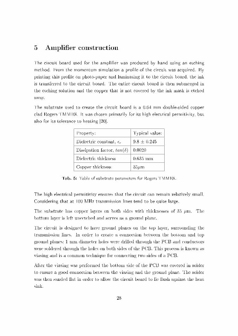
The cooling of the amplier is performed by mounting the amplier on a heatsink.
The heatsink consists of a block of aluminum which is tted with a water pipe
running through it. This enables for water cooling at a ow rate of 8 l/min. The
nished amplier can be seen in gure 14.
30
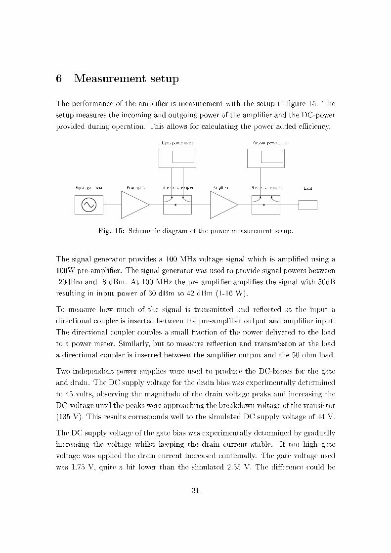
6 Measurement setup
The performance of the amplier is measurement with the setup in gure 15. The
setup measures the incoming and outgoing power of the amplier and the DC-power
provided during operation. This allows for calculating the power added eciency.
Signal generator Preamplier Directional coupler Amplier Directional coupler Load
Input power meter Output power meter
Fig. 15: Schematic diagram of the power measurement setup.
The signal generator provides a 100 MHz voltage signal which is amplied using a
100W pre-amplier. The signal generator was used to provide signal powers between
-20dBm and -8 dBm. At 100 MHz the pre-amplier amplies the signal with 50dB
resulting in input power of 30 dBm to 42 dBm (1-16 W).
To measure how much of the signal is transmitted and reected at the input a
directional coupler is inserted between the pre-amplier output and amplier input.
The directional coupler couples a small fraction of the power delivered to the load
to a power meter. Similarly, but to measure reection and transmission at the load
a directional coupler is inserted between the amplier output and the 50 ohm load.
Two independent power supplies were used to produce the DC-biases for the gate
and drain. The DC supply voltage for the drain bias was experimentally determined
to 45 volts, observing the magnitude of the drain voltage peaks and increasing the
DC-voltage until the peaks were approaching the breakdown voltage of the transistor
(135 V). This results corresponds well to the simulated DC supply voltage of 44 V.
The DC supply voltage of the gate bias was experimentally determined by gradually
increasing the voltage whilst keeping the drain current stable. If too high gate
voltage was applied the drain current increased continually. The gate voltage used
was 1.75 V, quite a bit lower than the simulated 2.55 V. The dierence could be
31

due to discrepancies between the simulation model of the transistor and the physical
transistor.
In order to measure the eciency of the amplier the DC-power provided needs to
be measured. The DC-current supplied to the output was measured using a current
probe connected to an oscilloscope. The probe is depicted in gure 16.
Fig. 16: Current sensor used to measure the drain current.
The eciency of the amplier could be calculated using equation 2.
The signal provided to the amplier during the power measurements consists of a
pulsed sinusoidal voltage of 3.5 µs pulses between delays of 66.5 µs for a total period
of 70 µs resulting in a duty cycle of 5 %.
The voltage waveforms at the drain and gate were measured using an oscilloscope
and two high voltage probes.
32
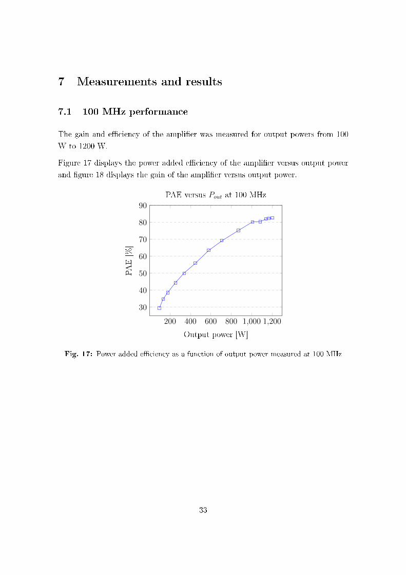
7 Measurements and results
7.1 100 MHz performance
The gain and eciency of the amplier was measured for output powers from 100
W to 1200 W.
Figure 17 displays the power added eciency of the amplier versus output power
and gure 18 displays the gain of the amplier versus output power.
200 400 600 800 1,000 1,200
30
40
50
60
70
80
90
Output power [W]
PAE[%]
PAE versus Pout at 100 MHz
Fig. 17: Power added eciency as a function of output power measured at 100 MHz
33

200 400 600 800 1,000 1,200
20
21
22
23
24
25
Output power [W]
Gain[dB]
Gain versus Pout at 100 MHz
Fig. 18: Power gain as a function of output power measured at 100 MHz
The results are close to what was expected from simulations with a maximum power
added eciency of 82.6% at an output power of 1202 W.
The drain voltage waveform was measured as well and is displayed in gure 19.
Fig. 19: Measured drain voltage waveform at 100 MHz
The waveform looks similar to simulations except that the voltage dips below zero
34
in between peaks and the hump shortly after the main peak.
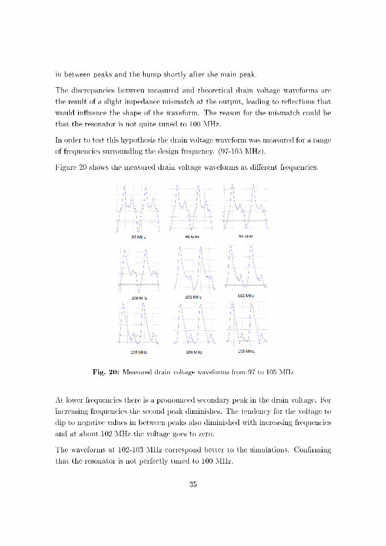
The discrepancies between measured and theoretical drain voltage waveforms are
the result of a slight impedance mismatch at the output, leading to reections that
would inuence the shape of the waveform. The reason for the mismatch could be
that the resonator is not quite tuned to 100 MHz.
In order to test this hypothesis the drain voltage waveform was measured for a range
of frequencies surrounding the design frequency. (97-105 MHz).
Figure 20 shows the measured drain voltage waveforms at dierent frequencies.
Fig. 20: Measured drain voltage waveforms from 97 to 105 MHz
At lower frequencies there is a pronounced secondary peak in the drain voltage. For
increasing frequencies the second peak diminishes. The tendency for the voltage to
dip to negative values in between peaks also diminished with increasing frequencies
and at about 102 MHz the voltage goes to zero.
The waveforms at 102-103 MHz correspond better to the simulations. Conrming
that the resonator is not perfectly tuned to 100 MHz.
35
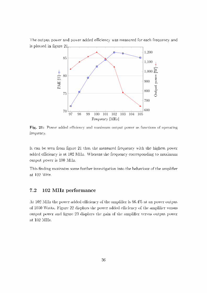
The output power and power added eciency was measured for each frequency and
is plotted in gure 21.
97 98 99 100 101 102 103 104 10570
75
80
85
600
700
800
900
1,000
1,100
1,200
Frequency [MHz]
PAE[%]
Outputpow
er[W
]
Fig. 21: Power added eciency and maximum output power as functions of operating
frequency.
It can be seen from gure 21 that the measured frequency with the highest power
added eciency is at 102 MHz. Whereas the frequency corresponding to maximum
output power is 100 MHz.
This nding motivates some further investigation into the behaviour of the amplier
at 102 MHz.
7.2 102 MHz performance
At 102 MHz the power added eciency of the amplier is 86.4% at an power output
of 1050 Watts. Figure 22 displays the power added eciency of the amplier versus
output power and gure 23 displays the gain of the amplier versus output power
at 102 MHz.
36

200 400 600 800 1,000 1,20030
40
50
60
70
80
90
Output power [W]
PAE[%]
PAE versus Pout at 102 MHz
Fig. 22: Power added eciency as a function of output power measured at 102 MHz
200 400 600 800 1,000 1,200
20
21
22
23
24
25
Output power [W]
Gain[dB]
Gain versus Pout at 102 MHz
Fig. 23: Power gain as a function of output power measured at 102 MHz
37
So far we have seen that the voltage waveforms correspond well with the waveforms
predicted in simulation. However, the principle of a switch mode amplier is that
of separating the voltage and current waveforms in time.
Therefore it is of interest to perform a simultaneous measurement of the voltage and
current waveforms in order to verify this separation of voltage and current.
However measuring the drain source current waveform without interfering with the
operation of the amplier is not trivial.
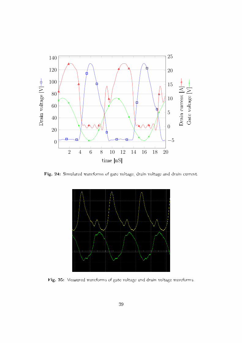
A possible way to measure the drain current waveform indirectly is to instead mea-
sure the gate voltage waveform with the assumption that the drain current should
essentially follow the gate voltage. This assumption is veried through simulations
of the amplier. Figure 24 shows a plot of the simulated waveforms of drain voltage,
drain current and gate voltage.
The real measurement of the gate and voltage waveforms can be seen in gure 25.
The gure serves to show the phase dierence between the gate and drain volt-
age. The gate voltage peaks and consequently the drain current peaks are situated
between the drain voltage peaks, as expected from theory and simulation.
38
2 4 6 8 10 12 14 16 18 20
0
20
40
60
80
100
120
140
−5
0
5
10
15
20
25
time [nS]
Drain
voltage[V]
Drain
current[A]
Gatevoltage[V]
Fig. 24: Simulated waveforms of gate voltage, drain voltage and drain current.
Fig. 25: Measured waveforms of gate voltage and drain voltage waveforms.
39
7.3 Heating
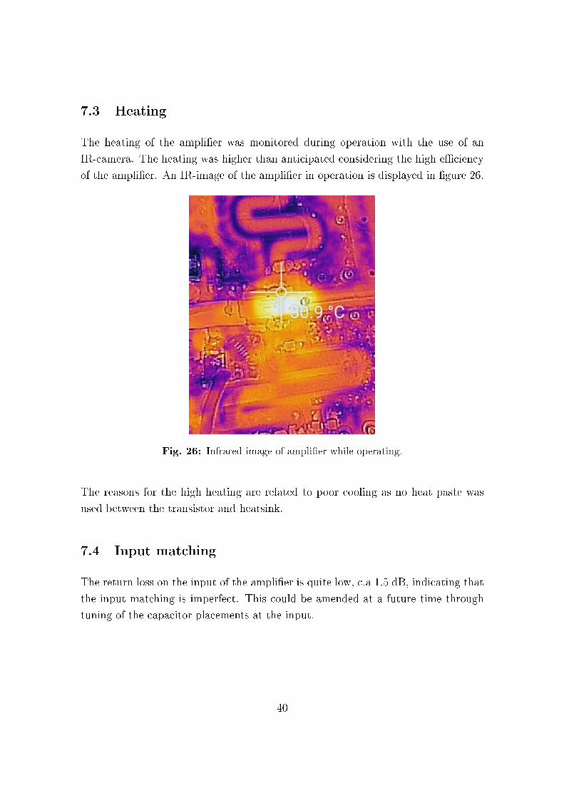
The heating of the amplier was monitored during operation with the use of an
IR-camera. The heating was higher than anticipated considering the high eciency
of the amplier. An IR-image of the amplier in operation is displayed in gure 26.
Fig. 26: Infrared image of amplier while operating.
The reasons for the high heating are related to poor cooling as no heat paste was
used between the transistor and heatsink.
7.4 Input matching
The return loss on the input of the amplier is quite low, c.a 1.5 dB, indicating that
the input matching is imperfect. This could be amended at a future time through
tuning of the capacitor placements at the input.
40

8 Conclusions and discussion
The feasibility of realizing a high-power, high-eciency, class E power amplier
using a simple single-ended design has been demonstrated. The amplier, based
on the power LDMOS-transistor 'BLF188XR', is capable of delivering 1200W peak
output power with a power added eciency of 82% in pulsed power operation at
100 MHz. At 102 MHz operation the peak output power is 1050W with a power
added eciency of 86%.
The design still has some issues, such as the low return loss at the input and the
heating of the transistor during operation. The input matching could be improved
through tuning of the size and position of the shunt capacitors at the input. However,
the input matching does aect the matching at the output, which poses a slight
challenge. The heating issues would presumably be alleviated by applying heat-
paste to the the transistor.
Although the produced amplier serves as a proof of concept, there are technical
challenges associated with implementation in a cyclotron that are not addressed.
For instance that the impedance of a cyclotron is variable.
41

9 Acknowledgments
I would like to thank Dragos Dancila for giving me the opportunity to do this project
and for his continuous support, good ideas, and helpful discussions. Invaluable help
was provided by Long Hoang Duc with everything from ADS to measurements.
Thanks to Tor Lofnes for his helpful thoughts and input on the experimental setup.
I also wish to thank Andreas Lundin for insights on the geometry of transistor
biasing. Finally I wish to thank the FREIA laboratory for hosting this master
work.
42
References
[1] Rodriguez, Erik A., et al. "New Dioxaborolane Chemistry Enables [18F]-
Positron-Emitting, Fluorescent [18F]-Multimodality Biomolecule Generation
from the Solid Phase." Bioconjugate chemistry 27.5 (2016): 1390-1399.
[2] Van Rijs, F. "Status and trends of silicon LDMOS base station PA technolo-
gies to go beyond 2.5 GHz applications". Radio and Wireless Symposium, 2008
IEEE. IEEE, 2008.
[3] Haapala, Linus, et al. "Kilowatt-level power amplier in a single-ended archi-
tecture at 352 MHz". Electronics Letters 52.18 (2016): pp. 1552-1554.
[4] Smirnov, Alexander, et al. "72 MHz Solid-state Amplier Power Test".
WEPME008, Proc. of Ipac2014, Dresden, Germany (2014): pp. 2270-2272 .
[5] Ortega-Gonzalez, Francisco Javier. "High power wideband class-E power am-
plier". IEEE Microwave and Wireless Components Letters 20.10 (2010): pp.
569-571.
[6] Krishnamurthy, K., et al. "100 W GaN HEMT power amplier module with>
60% eciency over 1001000 MHz bandwidth". Microwave Symposium Digest
(MTT), 2010 IEEE MTT-S International. IEEE, 2010.
[7] Maier, Florian A., et al. "A GaN-Based 10.1 MHz Class-F-1 300 W Continuous
Wave Amplier Targeting Industrial Power Applications". Compound Semicon-
ductor Integrated Circuit Symposium (CSICS), 2016 IEEE. IEEE, 2016.
[8] Tang, S., et al. "A 700W push-pull AlGaN/GaN power amplier for P-band
aerospace application". Electromagnetics in Advanced Applications (ICEAA),
2016 International Conference on. IEEE, 2016.
[9] Formicone, Gabriele, Je Burger, and James Custer. "A UHF 1-kW solid-state
power amplier for spaceborne SAR". RF/Microwave Power Ampliers for Ra-
dio and Wireless Applications (PAWR), 2017 IEEE Topical Conference on.
IEEE, 2017.
[10] Sokal, Nathan O., and Alan D. Sokal. "Class EA new class of high-eciency
tuned single-ended switching power ampliers." IEEE Journal of solid-state cir-
cuits 10.3 (1975): pp. 168-176.
43
[11] Raab, Frederick. "Idealized operation of the class E tuned power amplier".
IEEE transactions on Circuits and Systems 24.12 (1977): pp. 725-735.
[12] Besser, Les. "Avoiding RF Oscillation." Applied Microwave and Wireless 7
(1995): 44-44.
[13] Ampleon, "BLF188XR;BLF188XRS - Power LDMOS transistor" Rev.6 (2015).
[14] Adapted from: https://commons.wikimedia.org/wiki/File:EM_spectrum.sv
Retrieved September 4th 2017. Copyright 2007 by Philip Ronan. Adapted with
permission.
[15] Pozar, David M. "Microwave engineering". John Wiley & Sons, (2012)
[16] Grebennikov, Andrei, Nathan O. Sokal, and Marc J. Franco. "Switchmode RF
and microwave power ampliers". Academic Press, 2012.
[17] BLF188XR: Simulation model for ADS 2016. Ampleon. Published 2017-01-16.
Available from:
http://www.ampleon.com/products/broadcast/0-500-mhz-rf-power-
transistors/BLF188XR.html
[18] ADS Class E design equation template.
Available from:
http://www.keysight.com/nd/eesof-how-to-pa-series
[19] Kyung-Whan, Yeom. "Microwave circuit design". Pearson (2015). pp 705-717.
[20] TMM Thermoset microwave materials TMM3, TMM4, TMM6, TMM10,
TMM10i, TMM13i. Rogers corportation (2015).
44
A Appendix A
A.1 ADS equations
vmax = max(ts(vds)) (8)
PDC = vccmeas[0] · idc.i[0] (9)
Pout = real(0.5 · Vout[1] · conj(iout.i[1])) (10)
PAE = 100 · real((Pout − Pin)/PDC) (11)
VC1max = max(ts(vc1)) (12)
VC2max = max(ts(vc2)) (13)
45

B Appendix B
B.1 Electronics at high frequencies
The everyday AC applications in our home, like vacuum cleaners and toasters op-
erate at a frequency of 50 Hz. An electromagnetic wave with a frequency of 50 Hz
has a wavelength of several thousand kilometers. In these types of applications it
is safe to assume that the phase of a voltage signal remains unchanged over the
physical dimensions of the system, and that the only phase changes that needs to
be considered are those that arise from reactive components.
However, when the frequency of an electromagnetic wave increases; its wavelength
decreases proportionally and for high enough frequencies the wavelength of the elec-
trical signals in a system will be comparable to the physical dimensions of its com-
ponents.
At these higher frequencies classical circuit theory breaks down and is generally
unable to describe the function of high frequency circuits. This is because classical
circuit theory is a simplication of Maxwell's equations and is only valid as long as
the wave-nature of the signal is negligible.
This wave-nature of the voltage signal gives rise to a multitude of eects which
needs to be taken into consideration. For instance, voltage signals will be reected
at discontinuities in impedance, for example at transition between a conductor and
a load.
These eects start becoming signicant when the wavelength of the electrical signal
is comparable to the electrical system of interest. In our case this will be on the
scale of meters which corresponds to frequencies of about a hundred megahertz
These are the same frequencies at which standard FM-radio is sent. The part of the
electromagnetic spectrum corresponding to these frequencies can be seen marked as
"FM-radio" in gure 27.
46

Fig. 27: The electromagnetic spectrum. [14]
The consequence of all this is that since the instantaneous value of voltage and
current changes over the length of components, voltages are not necessarily the
most useful way of characterizing a circuit. Therefore other parameters such as
power, reection coecient, and S-parameters are used instead. These concepts will
be described further in the following sections.
B.1.1 Transmission lines and distributed elements
Conductors and the dimensions of components are neglected at low frequencies, but
since voltages change with distance at high frequencies conductors can have a very
signicant impact; and are often designed to be crucial components in circuits.
In a high frequency context conductors are referred to as transmission lines. A
voltage signal propagating through a transmission line will give rise to a current.
The ratio between the voltage and current on the line is its characteristic impedance
(denoted Z0). The characteristic impedance of the transmission line is determined
by its dimensions and material properties.
The standard impedance used in most systems is 50 Ohms. It was chosen as a
compromise between having good power handling and low losses.
If one wishes to connect a 50 Ohm source with a 50 Ohm load the characteristic
impedance of the transmission line will also have to be 50 Ohms or else reections
will arise due to the discontinuity in impedance.
The length of a transmission line will not aect its characteristic impedance. How-
ever, the phase of a voltage signal will change with the length of the line. Hence the
47
ZinZ0
lZL
Fig. 28: Input impedance Zin of a transmission line of length l with characteristic
impedance Z0 connected to a load ZL
length will still aect what impedance is 'seen' at the input of a transmission line,
making it crucial in circuit design.
The total input impedance of a transmission line with characteristic impedance Z0
terminated with a load ZL is determined by the following expression[15]:
Zin = Z0ZL + jZ0 tan(βl)
Z0 + jZL tan(βl)(14)
Where Zin is the input impedance, Z0 is the characteristic impedance of the trans-
mission line, l is the length of the line, β = 2πλis the wave number, and ZL is the
load impedance.
This expression allows choosing what impedance is seen from a point by choosing
the dimensions of a transmission line.
B.1.2 Reection Coecients
As previously mentioned due its wave-nature; a voltage signal will cause reections
at discontinuities in impedance. The ratio of the reected to the transmitted part of
a voltage signal is the reection coecient, which acts as a measure of the mismatch
in impedances. Reection coecients are a very useful concept and is used frequently
in RF circuit design.
Γ =VRVI
(15)
When designing an RF circuit it is often the case that certain reection coecients
are desired. For instance it is a very common goal to minimize the magnitude of the
48

reection coecient in order to maximize transmitted power; for instance from an
amplier to a load. Another reason for wanting to minimize the reection coecient
is that high reection coecients can be problematic, since large reected voltages
can damage signal generators, ampliers and other sensitive equipment.
However there are examples when minimizing the reection coecient is not the
main goal. For instance if the goal is to maximize eciency or minimizing noise
of an amplier rather than maximizing the transmitted power. In practice there is
often a trade-o when choosing reection coecients, and often the most suitable
coecient is a compromise between several goals.
This begs the question, how can reection coecients be chosen?
It can be shown that the reection coecient at the transition between two impedances
Z1 and Z2 can be expressed solely in terms of these impedances as [15]:
Γ =Z2 − Z1
Z2 + Z1
(16)
For a voltage signal which transitions from Z1 to Z2
So, in order to choose our desired reection coecient we need to be able to choose
the impedances in our circuit. However, the impedances in a circuit is not free
to choose. For example the output impedance of a transistor in an amplier is
determined by the transistor and its biasing conditions, and is often a few ohms. As
opposed to a typical load impedance which is 50 Ohms.
By using transmission lines and or lumped components like capacitors and inductors
one can make any impedance appear to be any other impedance at the input of an
intermediate network. This is known as impedance matching. A network that can
match two impedances is called a matching network and it allows a designer to
produce a reection coecient of choice.
From equation (14) it is possible to design matching networks analytically by nding
a solution that transforms the impedance into another.
B.1.3 Impedance matching and the Smith chart
Impedance matching can also be performed graphically using a Smith chart
49
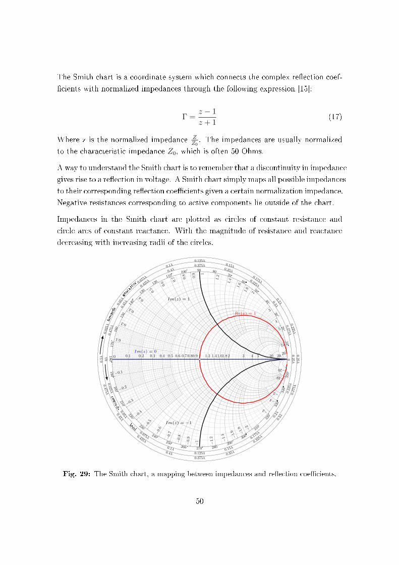
The Smith chart is a coordinate system which connects the complex reection coef-
cients with normalized impedances through the following expression [15]:
Γ =z − 1
z + 1(17)
Where z is the normalized impedance ZZ0. The impedances are usually normalized
to the characteristic impedance Z0, which is often 50 Ohms.
A way to understand the Smith chart is to remember that a discontinuity in impedance
gives rise to a reection in voltage. A Smith chart simply maps all possible impedances
to their corresponding reection coecients given a certain normalization impedance.
Negative resistances corresponding to active components lie outside of the chart.
Impedances in the Smith chart are plotted as circles of constant resistance and
circle arcs of constant reactance. With the magnitude of resistance and reactance
decreasing with increasing radii of the circles.
towards
generator
towards
load
0.5λ
0.475λ
0.45λ
0.425λ
0.4λ0.375λ
0.35λ
0.325λ
0.3λ
0.27
5λ
0.25λ
0.225λ
0.2λ
0.175λ
0.15λ
0.125λ
0.1λ
0.075λ
0.05λ
0.02
5λ0λ
0.025λ
0.05λ
0.075λ
0.1λ0.125λ
0.15λ
0.175λ
0.2λ
0.22
5λ
0.25λ
0.275λ
0.3λ
0.325λ
0.35λ
0.375λ
0.4λ
0.425λ
0.45λ
0.47
5λ
0°
10°
20°
30°
40°
50°
60°
70°
80°
90°
100°
110°
120°
130°
140°
150°
160°
170°
180°
190°
200°
210°
220°
230°
240°
250°
260° 270°280°
290°300°
310°
320°
330°
340°
350°
0.1 0.2 0.3 0.4 0.5 0.6 0.7 0.80.9 1 1.2 1.4 1.61.8 2 3 4 5 10 200
0.1
0.2
0.3
0.4
0.5
0.6 0.
7 0.8 0.9 1
1.2
1.4
1.6
1.8
2
3
4
5
10
20
−0.1
−0.2
−0.3
−0.4
−0.5
−0.
6
−0.
7
−0.
8
−0.
9
−1 −1.
2
−1.
4 −1.
6 −1.8 −2
−3
−4
−5
−10
−20
Re(z) = 1
Im(z) = 1
Im(z) = −1
Im(z) = 0
Fig. 29: The Smith chart, a mapping between impedances and reection coecients.
50

The reection coecient for a given impedance is found from the intersection of
impedance point and constant Γ-circle.
The magnitude of the reection coecient is given by the distance from the center
of the chart, and its phase is read from the perimeter of the chart.
Since we established earlier that the dimensions of components can change the
impedance that is seen from a point, it should come as no surprise that compo-
nents and their dimensions can be used to move in the Smith chart.
As an example, say that we want to match a 25+j25Ω source to a 50 Ω load for a
1 GHz system. One way of doing this would be to add a series transmission line
in order to move clockwise around a circle of constant reection coecient until we
reach the 50Ω circle of constant resistance. Then add a series capacitance to move
counter-clockwise along the 50 Ω constant resistance circle until we reach the 50+j0
Ω point at the center of the chart. It is worth noting that this path is one of an
innite number of possible paths in the Smith chart. Therefore an innite number
of equally valid matching networks could be made.
towards
generator
towards
load
0.5λ
0.475λ
0.45λ
0.425λ
0.4λ0.375λ
0.35λ
0.325λ
0.3λ
0.27
5λ
0.25λ
0.225λ
0.2λ
0.175λ
0.15λ
0.125λ
0.1λ
0.075λ
0.05λ
0.02
5λ0λ
0.025λ
0.05λ
0.075λ
0.1λ0.125λ
0.15λ
0.175λ
0.2λ
0.22
5λ
0.25λ
0.275λ
0.3λ
0.325λ
0.35λ
0.375λ
0.4λ
0.425λ
0.45λ
0.47
5λ
0°
10°
20°
30°
40°
50°
60°
70°
80°
90°
100°
110°
120°
130°
140°
150°
160°
170°
180°
190°
200°
210°
220°
230°
240°
250°
260° 270°280°
290°300°
310°
320°
330°
340°
350°
0.1 0.2 0.3 0.4 0.5 0.6 0.7 0.80.9 1 1.2 1.4 1.61.8 2 3 4 5 10 200
0.1
0.2
0.3
0.4
0.5
0.6 0.
7 0.8 0.9 1
1.2
1.4
1.6
1.8
2
3
4
5
10
20
−0.1
−0.2
−0.3
−0.4
−0.5
−0.
6
−0.
7
−0.
8
−0.
9
−1 −1.
2
−1.
4 −1.
6 −1.8 −2
−3
−4
−5
−10
−20
Series capacitance
Transmission line
Fig. 30: The impedance matching of a 25 +j25Ω source to a 50Ω load.
The length of the transmission line can be found from the change in angle of the
reection coecient. We started at an angle of 117 and ended at 64, which is a
dierence of 53 degrees. This corresponds to a transmission line length of 53720λ =
0.0736λ. (720 since a voltage signal travels through the transmission line twice)
The size of the series capacitor can be found from the formula of capacitor impedance:
51

ZC = 1jωC
We moved from the point 50 +j50 Ω to 50 + j0 Ω so the impedance of
our capacitor is -j50Ω. Thus: 1jωC
= −j50Ω =⇒ 1ωC
= 50 =⇒ C = 150ω
= 3.18pF
Consequently our impedance matching network would look as depicted in gure 31.
25 + j25Ω 50Ω
Matching network
Transmission line
0.07λ
Series capacitor
3.18pF
Fig. 31: Matching network between the impedances 25 +j25Ω and 50Ω for the frequency
1 GHz
B.1.4 Scattering parameters
A useful concept in RF engineering is scattering parameters or 'S-parameters'.
With the use of S-parameters any electrical system can be described as an N-port.
An N-port is an unknown network or a 'black box' featuring N pairs of terminals
referred to as ports. For a voltage signal that enters a port some of the signal will
be reected back to that port, some parts may exit at other ports. Exactly which
paths the signal take within the black box is not essential and system is completely
described by the voltages seen on each port when a voltage is introduced at each
other port.
More specically an S-parameter Sxy is dened as the ratio between the voltage seen
at port x for a voltage entering port y. With the added condition that all other ports
are terminated in matched loads so as to not contribute to the signal via additional
reections.
The S-parameters are complex numbers since they take into account possible changes
in both the amplitude and the phase of the voltage.
An N-port system can then be described using an N×N S-parameter matrix. The
columns of the matrix each correspond to an input port and the rows to an output
port, so that the element in column x and row y corresponds to the s-parameter Sxy.
The elements on the diagonal of the S-matrix are reection coecients, since they
52

describe what voltage is seen returning to the same input into witch the voltage
signal entered. The o-diagonal elements are transmission coecients since they
describe what voltage is seen at one input when a voltage signal enters another
input.
A special case of particular interest is that of the 2-port system. This is because an
amplier can be seen as a two port with one input port and one output port.
b1
a1
a2
b2
Fig. 32: A two-port network with incoming voltages a1 and a2, and outgoing voltages b1
and b2
The incoming and outgoing voltage signals of the two port system can be related
using the systems S-matrix as follows:a1a2
S11 S12
S21 S22
=
b1b2
In the context of ampliers the S-parameters can be interpreted in the following
way:
S11 - Input reection coecient
S12 - Reverse isolation parameter
S21 - Voltage gain
S22 - Output reection coecient
The parameter S12 requires some further explanation: It is a measure of how much
of a voltage signal that is transmitted from the output to the input of the amplier.
An ideal amplier would have its input and output perfectly isolated from each other
and would therefore have a S12 parameter equal to zero. Devices with a zero reverse
isolation parameter are referred to as being 'unilateral'. However, in real devices
we need to consider the bidirectional case, and the S12 parameter is of importance
when determining the stability of an amplier.
53


![Ampli cateur audio de classe D - f-legrand.fr€¦ · Ampli cateur audio de classe D 1. Introduction Ce document décrit la réalisation d'un ampli cateur audio de classe D ([1]),](https://static.documents.pub/doc/80x56/61072f6c7cf27371ea366aef/ampli-cateur-audio-de-classe-d-f-ampli-cateur-audio-de-classe-d-1-introduction.jpg)


