2-A DUAL NON-SYNCHRONOUS CONVERTER WITH INTEGRATED HIGH-SIDE MOSFET
23• 4.5-V to 28-V Input Range Device Ratings 2• Output Voltage Range 0.8 V to 90% of Input Electrical Characteristics 3
Voltage Device Information 9• Output Current Up to 2 A Application Information 12
Design Examples 32• Two Fixed Switching Frequency Versions:Additional References 44– TPS54283: 300 kHz
– TPS54286: 600 kHz• Two Selectable Levels of Overcurrent
Protection (Output 2) TPS54283 and TPS54286 are dual outputnon-synchronous buck converters capable of• 0.8-V 1.5% Voltage Referencesupporting 2-A output applications that operate from a• 2.1-ms Internal Soft Start 4.5-V to 28-V input supply voltage, and require output
• Dual PWM Outputs 180° Out-of-Phase voltages between 0.8 V and 90% of the input voltage.• Ratiometric or Sequential Startup Modes With internally-determined operating frequency, soft
Selectable by a Single Pin start time, and control loop compensation, these• 100-mΩ Internal High-Side MOSFETs converters provide many features with a minimum of
external components. Channel 1 overcurrent• Current Mode Controlprotection is set at 3 A, while Channel 2 overcurrent• Internal Compensation (See Page 16) protection level is selected by connecting a pin to
• Pulse-by-Pulse Overcurrent Protection ground, to BP, or left floating. The setting levels areused to allow for scaling of external components for• Thermal Shutdown Protection at 148°Capplications not needing the full load capability of• 14-Pin PowerPAD™ HTSSOP package both outputs.
The outputs may be enabled independently, or maybe configured to allow either ratiometric or sequential• Set Top Boxstartup sequencing. Additionally, the two outputs may• Digital TV also be powered from different sources.
• Power for DSP• Consumer Electronics
1
Please be aware that an important notice concerning availability, standard warranty, and use in critical applications ofTexas Instruments semiconductor products and disclaimers thereto appears at the end of this data sheet.
2PowerPAD is a trademark of Texas Instruments.3All other trademarks are the property of their respective owners.
These devices have limited built-in ESD protection. The leads should be shorted together or the device placed in conductive foamduring storage or handling to prevent electrostatic damage to the MOS gates.
ORDERING INFORMATION (1)
PART NUMBER OPERATING FREQUENCY (kHz) PACKAGE MEDIA UNITS (Pieces)
TPS54283PWP Tube 90300
TPS54283PWPR Tape and Reel 2000Plastic 14-Pin HTSSOP
TPS54286PWP Tube 90600
TPS54286PWPR Tape and Reel 2000
(1) For the most current package and ordering information see the Package Option Addendum at the end of this document, or see the TIweb site at www.ti.com.
VALUE UNIT
PVDD1, PVDD2, EN1, EN2 30
BOOT1, BOOT2 VSW+ 7
SW1, SW2 –2 to 30
Input voltage range SW1, SW2 transient (< 50ns) –3 to 31 V
BP 6.5
SEQ, ILIM2 –0.3 to 6.5
FB1, FB2 –0.3 to 3
SW1, SW2 output current 7 A
BP load current 35 mA
Tstg Storage temperature –55 to +165
TJ Operating temperature –40 to +150 °C
Soldering temperature +260
(1) Permanent device damage may occur if Absolute Maximum Ratings are exceeded. Functional operation should be limited to theRecommended DC Operating Conditions detailed in this data sheet. Exposure to conditions beyond the operational limits for extendedperiods of time may affect device reliability.
MIN MAX UNITVPVDD2 Input voltage 4.5 28 VTJ Operating junction temperature –40 +125 °C
MIN UNITHuman body model 2kCDM 1.5k VMachine Model 250
THERMAL IMPEDANCEJUNTION-TO-THERMAL PAD TA = +25°C, NO AIR FLOW TA = +85°C, NO AIR FLOW
PACKAGE (°C/W) POWER RATING (W) POWER RATING (W)
Plastic 14-Pin HTSSOP (PWP) 2.07 (4) 1.6 1.0
(1) For more information on the PWP package, refer to TI Technical Brief (SLMA002A).(2) TI device packages are modeled and tested for thermal performance using printed circuit board designs outlined in JEDEC standards
JESD 51-3 and JESD 51-7.(3) For application information, see the Power Derating section.(4) TJ-A = +40°C/W
VUV1Low-level output threshold to declare a fault Measured at feedback pin. 670 mV
VUV2
THICCUP(1) Hiccup timeout 10 ms
tON1(oc)(1)
Minimum overcurrent pulse width 90 150 nstON2(oc)
(1)
(1) Ensured by design. Not production tested.(2) When both outputs are started simultaneously, a 20-mA current source charges the BP capacitor. Faster times are possible with a lower
BP capacitor value. More information can be found in the Input UVLO and Startup section.
Input supply to the high side gate driver for Output 1. Connect a 22-nF to 82-nF capacitor from this pinto SW1. This capacitor is charged from the BP pin voltage through an internal switch. The switch isBOOT1 2 I turned ON during the OFF time of the converter. To slow down the turn ON of the internal FET, a smallresistor (1 Ω to 3 Ω) may be placed in series with the bootstrap capacitor.Input supply to the high side gate driver for Output 2. Connect a 22-nF to 82-nF capacitor from this pinto SW2. This capacitor is charged from the BP pin voltage through an internal switch. The switch isBOOT2 13 I turned ON during the OFF time of the converter. To slow down the turn ON of the internal FET, a smallresistor (1 Ω to 3 Ω) may be placed in series with the bootstrap capacitor.Regulated voltage to charge the bootstrap capacitors. Bypass this pin to GND with a low ESR (4.7-µFBP 11 - to 10-µF X7R or X5R preferred) ceramic capacitor.Active low enable input for Output 1. If the voltage on this pin is greater than 1.55 V, Output 1 isdisabled (high-side switch is OFF). A voltage of less than 0.9 V enables Output 1 and allows soft start ofEN1 5 I Output 1 to begin. An internal current source drives this pin to PVDD2 if left floating. Connect this pin toGND to force "always ON" operation.Active low enable input for Output 2. If the voltage on this pin is greater than 1.55 V, Output 2 isdisabled (high-side switch is OFF). A voltage of less than 0.9 V enables Output 2 and allows soft start ofEN2 6 I Output 2 to begin. An internal current source drives this pin to PVDD2 if left floating. Connect this pin toGND to force "always ON" operation.Voltage feedback pin for Output 1. The internal transconductance error amplifier adjusts the PWM forOutput 1 to regulate the voltage at this pin to the internal 0.8-V reference. A series resistor divider from
FB1 7 I Output 1 to ground, with the center connection tied to this pin, determines the value of the regulatedoutput voltage. Compensation for the feedback loop is provided internally to the device. See FeedbackLoop and Inductor-Capacitor (L-C) Filter section for further information.Voltage feedback pin for Output 2. The internal transconductance error amplifier adjusts the PWM forOutput 2 to regulate the voltage at this pin to the internal 0.8-V reference. A series resistor divider from
FB2 8 I Output 2 to ground, with the center connection tied to this pin, determines the value of the regulatedOutput voltage. Compensation for the feedback loop is provided internally to the device. See FeedbackLoop and Inductor-Capacitor (L-C) Filter section for further information.
GND 4 - Ground pin for the device. Connect directly to Thermal Pad.Current limit adjust pin for Output 2 only. This function is intended to allow a user with asymmetricalload currents (Output 1 load current much greater than Output 2 load current) to optimize component
ILIM2 9 I scaling of the lower current output while maintaining proper component derating in a overcurrent faultcondition. The discrete levels are available as shown in Table 2. Note: An internal 2-resistor divider(150-kΩ each) connects BP to ILIM2 and to GND.Power input to the Output 1 high side MOSFET only. This pin should be locally bypassed to GND with aPVDD1 1 I low ESR ceramic capacitor of 10-µF or greater.The PVDD2 pin provides power to the device control circuitry, provides the pull-up for the EN1 and EN2pins and provides power to the Output 2 high-side MOSFET. This pin should be locally bypassed toPVDD2 14 I GND with a low ESR ceramic capacitor of 10-µF or greater. The UVLO function monitors PVDD2 andenables the device when PVDD2 is greater than 4.1 V.
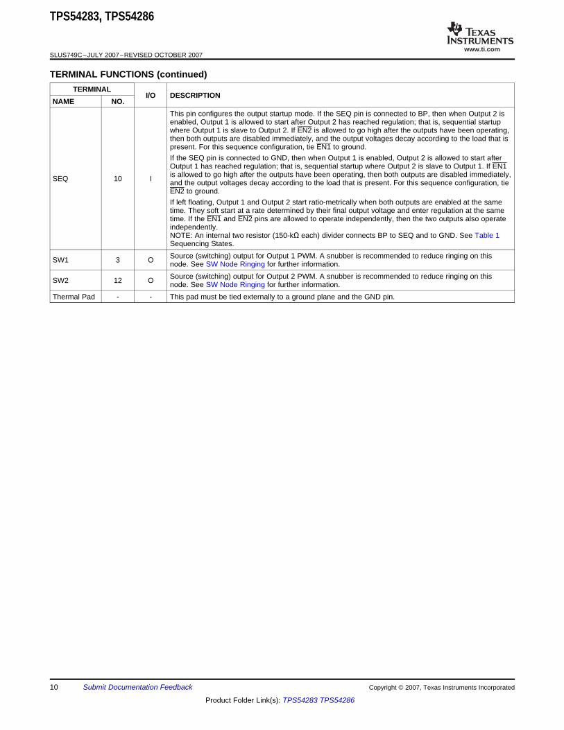
This pin configures the output startup mode. If the SEQ pin is connected to BP, then when Output 2 isenabled, Output 1 is allowed to start after Output 2 has reached regulation; that is, sequential startupwhere Output 1 is slave to Output 2. If EN2 is allowed to go high after the outputs have been operating,then both outputs are disabled immediately, and the output voltages decay according to the load that ispresent. For this sequence configuration, tie EN1 to ground.If the SEQ pin is connected to GND, then when Output 1 is enabled, Output 2 is allowed to start afterOutput 1 has reached regulation; that is, sequential startup where Output 2 is slave to Output 1. If EN1is allowed to go high after the outputs have been operating, then both outputs are disabled immediately,SEQ 10 I and the output voltages decay according to the load that is present. For this sequence configuration, tieEN2 to ground.If left floating, Output 1 and Output 2 start ratio-metrically when both outputs are enabled at the sametime. They soft start at a rate determined by their final output voltage and enter regulation at the sametime. If the EN1 and EN2 pins are allowed to operate independently, then the two outputs also operateindependently.NOTE: An internal two resistor (150-kΩ each) divider connects BP to SEQ and to GND. See Table 1Sequencing States.Source (switching) output for Output 1 PWM. A snubber is recommended to reduce ringing on thisSW1 3 O node. See SW Node Ringing for further information.Source (switching) output for Output 2 PWM. A snubber is recommended to reduce ringing on thisSW2 12 O node. See SW Node Ringing for further information.
Thermal Pad - - This pad must be tied externally to a ground plane and the GND pin.
The TPS54283 and TPS54286 are dual output non-synchronous converters. Each PWM channel contains aninternally-compensated error amplifier, current mode pulse width modulator (PWM), switch MOSFET, enable,and fault protection circuitry. Common to the two channels are the internal voltage regulator, voltage reference,clock oscillator, and output voltage sequencing functions.
DESIGN HINT
The TPS5428x contains internal slope compensation and loop compensationcomponents; therefore, the external L-C filter must be selected appropriately so thatthe resulting control loop meets criteria for stability. This approach differs from anexternally-compensated controller, where the L-C filter is generally selected first, andthe compensation network is found afterwards. (See Feedback Loop and L-C FilterSelection section.)
NOTE:
Unless otherwise noted, the term TPS5428x applies to both the TPS54283 andTPS54286. Also, unless otherwise noted, a label with a lowercase x appended impliesthe term applies to both outputs of the two modulator channels. For example, the termENx implies both EN1 and EN2. Unless otherwise noted, all parametric values givenare typical. Refer to the Electrical Characteristics for minimum and maximum values.Calculations should be performed with tolerance values taken into consideration.
The bandgap cell common to both outputs, trimmed to 800 mV.
The oscillator frequency is internally fixed at two times the SWx node switching frequency. The two outputs areinternally configured to operate on alternating switch cycles (that is, 180° out of phase).
When the voltage at the PVDD2 pin is less than 4.1 V, a portion of the internal bias circuitry is operational, andall other functions are held OFF. All of the internal MOSFETs are also held OFF. When the PVDD2 voltage risesabove the UVLO turn-on threshold, the state of the enable pins determines the remainder of the internal startupsequence. If either output is enabled (ENx pulled low), the BP regulator turns on, charging the BP capacitor witha 20 mA current. When the BP pin is greater than 4 V, PWM is enabled and soft start begins, depending on theSEQ mode of operation and the EN1 and EN2 settings.
Note that the internal regulator and control circuitry are powered from PVDD2. The voltage on PVDD1 may behigher or lower than PVDD2. (See the Dual Supply Operation section.)
Each output has a dedicated (active low) enable pin. If left floating, an internal current source pulls the pin toPVDD2. By grounding, or by pulling the ENx pin to below approximately 1.2 V with an external circuit, theassociated output is enabled and soft start is initiated.
If both enable pins are left in the high state, the device operates in a shutdown mode, where the BP regulator isshut down and minimal functions are active. The total standby current from both PVDD pins is approximately70 µA at 12-V input supply.
An R-C connected to an ENx pin may be used to delay the turn-on of the associated output after power isapplied to PVDDx (see Figure 15). After power is applied to PVDD2, the voltage on the ENx pin slowly decaystowards ground. Once the voltage decays to approximately 1.2 V, then the output is enabled and the startupsequence begins. If it is desired to enable the outputs of the device immediately upon the application of power toPVDD2, then omit these two components and tie the ENx pin to GND directly.
If an R-C circuit is used to delay the turn-on of the output, the resistor value must be much less than 1.2 V / 6µAor 200 kΩ. A suggested value is 51 kΩ. This resistor value allows the ENx voltage to decay below the 1.2-Vthreshold while the 6-µA bias current flows.
The capacitor value required to delay the startup time (after the application of PVDD2) is shown in Equation 1.
where:• R and C are the timing components• VTH is the 1.2-V enable threshold voltage• IENx is the 6µA enable pin biasing current
Other enable pin functionality is dictated by the state of the SEQ pin. (See the Output Voltage Sequencingsection.)
Figure 15. Startup Delay Schematic Figure 16. Startup Delay with R-C on Enable
DESIGN HINT
If delayed output voltage startup is not necessary, simply connect EN1 and EN2 toGND. This configuration allows the outputs to start immediately on valid application ofPVDD2.
If ENx is allowed to go high after the Outputx has been in regulation, the upper MOSFET shuts off, and theoutput decays at a rate determined by the output capacitor and the load. The internal pulldown MOSFET remainsin the OFF state. (See the Bootstrap for N-Channel MOSFET section.)
The TPS5428x allows single-pin programming of output voltage startup sequencing. During power-on, the stateof the SEQ pin is detected. Based on whether the pin is tied to BP, to GND, or left floating, the outputs behaveas described in Table 1.
Table 1. Sequence StatesSEQ PIN STATE MODE EN1 EN2
Ignored by the device when VEN2 <enable threshold voltage
Tie EN1 to < enable threshold voltagefor BP to be active when VEN2 >BP Sequential, Output 2 then Output 1 Activeenable threshold voltage
Tie EN1 to > enable threshold voltagefor low quiescent current (BP inactive)when VEN2 > enable threshold voltage
Ignored by the device when VEN1 <enable threshold voltage
Tie EN2 to < enable threshold voltagefor BP to be active when VEN1 >GND Sequential, Output 1 then Output 2 Active enable threshold voltage
Tie EN2 to > enable threshold voltagefor low quiescent current (BP inactive)when VEN1 > enable threshold voltage
Independent or Ratiometric, Output 1 Active. EN1 and EN2 must be tied Active. EN1 and EN2 must be tied(floating) and Output 2 together for Ratiometric startup. together for Ratiometric startup.
If the SEQ pin is connected to BP, then when Output 2 is enabled, Output 1 is allowed to start approximately 400µs after Output 2 has reached regulation; that is, sequential startup where Output 1 is slave to Output 2. If EN2
is allowed to go high after the outputs have been operating, then both outputs are disabled immediately, and theoutput voltages decay according to the load that is present.
If the SEQ pin is connected to GND, then when Output 1 is enabled, Output 2 is allowed to start approximately400 µs after Output 1 has reached regulation; that is, sequential startup where Output 2 is slave to Output 1. IfEN1 is allowed to go high after the outputs have been operating, then both outputs are disabled immediately,and the output voltages decay according to the load that is present.
Figure 17. SEQ Pin TIed to BP Figure 18. SEQ Pin Tied to GND
An R-C network connected to the ENx pin may be used in addition to the SEQ pin insequential mode to delay the startup of the first output voltage. This approach may benecessary in systems with a large number of output voltages and elaborate voltagesequencing requirements. See Enable and Timed Turn On of the Outputs.
If the SEQ pin is left floating, Output 1 and Output 2 each start ratiometrically when both outputs are enabled atthe same time. Output 1 and Output 2 soft start at a rate that is determined by the respective final outputvoltages and enter regulation at the same time. If the EN1 and EN2 pins are allowed to operate independently,then the two outputs also operate independently.
Figure 19. SEQ Pin Floating
Each output has a dedicated soft start circuit. The soft start voltage is an internal digital reference ramp to one oftwo noninverting inputs of the error amplifier. The other input is the (internal) precision 0.8-V reference. The totalramp time for the FB voltage to charge from 0 V to 0.8 V is about 2.1 ms. During a soft start interval, theTPS5428x output slowly increases the voltage to the noninverting input of the error amplifier. In this way, theoutput voltage ramps up slowly until the voltage on the noninverting input to the error amplifier reaches theinternal 0.8 V reference voltage. At that time, the voltage at the noninverting input to the error amplifier remainsat the reference voltage.
NOTE:
To avoid a disturbance in the output voltage during the stepping of the digital softstart, a minimum output capacitance of 50 µF is recommended. Also see FeedbackLoop and Inductor-Capacitor (L-C) Filter Selection Once the filter and compensationcomponents have been established, laboratory measurements of the physical designshould be performed to confirm converter stability.
During the soft start interval, pulse-by-pulse current limiting is in effect. If an overcurrent pulse is detected, sixPWM pulses are skipped to allow the inductor current to decay before another PWM pulse is applied. (See theOutput Overload Protection section.) There is no pulse skipping if a current limit pulse is not detected.
DESIGN HINT
If the rate of rise of the input voltage (PVDDx) is such that the input voltage is too low
to support the desired regulation voltage by the time Soft Start has completed, thenthe output UV circuit may trip and cause a hiccup in the output voltage. In this case,use a timed delay startup from the ENx pin to delay the startup of the output until thePVDDx voltage has the capability of supporting the desired regulation voltage. SeeOperating Near Maximum Duty Cycleand Maximum Output Capacitance for relatedinformation.
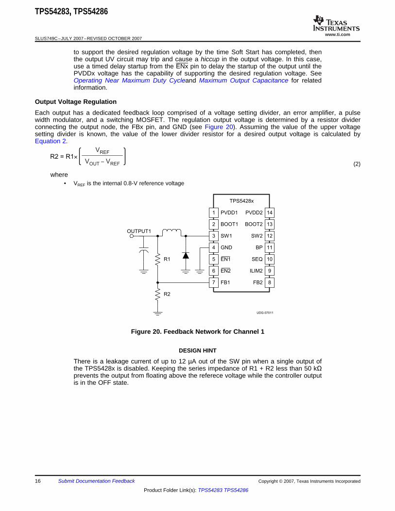
Each output has a dedicated feedback loop comprised of a voltage setting divider, an error amplifier, a pulsewidth modulator, and a switching MOSFET. The regulation output voltage is determined by a resistor dividerconnecting the output node, the FBx pin, and GND (see Figure 20). Assuming the value of the upper voltagesetting divider is known, the value of the lower divider resistor for a desired output voltage is calculated byEquation 2.
where• VREF is the internal 0.8-V reference voltage
Figure 20. Feedback Network for Channel 1
DESIGN HINT
There is a leakage current of up to 12 µA out of the SW pin when a single output ofthe TPS5428x is disabled. Keeping the series impedance of R1 + R2 less than 50 kΩprevents the output from floating above the referece voltage while the controller outputis in the OFF state.
Feedback Loop and Inductor-Capacitor (L-C) Filter Selection
TPS5428x
FB
CCOMP
11.5 kW
+
Error Amplifier
0.8 VREF
BOOT
SW
+
RCOMP
Offset f(IDRAIN
)
PWM to
SwitchISLOPE
ICOMP
TPS54283
TPS54286
RCOMP
(kW)
CCOMP
(pF)
700
700
40
20
UDG-07012
ICOMP
- ISLOPE
x2
TPS54283,, TPS54286
SLUS749C–JULY 2007–REVISED OCTOBER 2007
In the feedback signal path, the output voltage setting divider is followed by an internal gM-type error amplifierwith a typical transconductance of 30 µS. An internal series connected R-C circuit from the gM amplifier output toground serves as the compensation network for the converter. The signal from the error amplifier output is thenbuffered and combined with a slope compensation signal before it is mirrored to be referenced to the SW node.Here, it is compared with the current feedback signal to create a pulse-width-modulated (PWM) signal-fed todrive the upper MOSFET switch. A simplified equivalent circuit of the signal control path is depicted in Figure 21.
NOTE:
Noise coupling from the SWx node to internal circuitry of BOOTx may impact narrowpulse width operation, especially at load currents less than 1 A. See SW NodeRinging for further information on reducing noise on the SWx node.
Figure 21. Feedback Loop Equivalent Circuit
A more conventional small signal equivalent block diagram is shown in Figure 22. Here, the full closed loopsignal path is shown. Because the TPS5428x contains internal slope compensation and loop compensationcomponents, the external L-C filter must be selected appropriately so that the resulting control loop meets criteriafor stability. This approach differs from an externally-compensated controller, where the L-C filter is generallyselected first, and the compensation network is found afterwards. To find the appropriate L and C filtercombination, the Output-to-Vc signal path plots (see the next section) of gain and phase are used along withother design criterial to aid in finding the combinations that best results in a stable feedback loop.
The following figures plot the TPS5428x Output-to-Vc gain and phase versus frequency for various duty cycles(10%, 30%, 50%, 70%, 90%) at three (200 mA, 400 mA, 600 mA) peak-to-peak ripple current levels. The loopresponse curve selected to compensate the loop is based on the duty cycle of the application and the ripplecurrent in the inductor. Once the curve has been selected and the inductor value has been calculated, the outputcapacitor is found by calculating the L-C resonant frequency required to compensate the feedback loop. A briefexample follows the curves.
Note that the internal error amplifier compensation is optimized for output capacitors with an ESR zero frequencybetween 20kHz and 60kHz. See the following sections for further details.
GAIN AND PHASE GAIN AND PHASEvs vs
FREQUENCY FREQUENCY
Figure 23. TPS54283 at 200-mAp-p Ripple Current Figure 24. TPS54283 at 400-mAp-p Ripple Current
Figure 25. TPS54283 at 600-mAp-p Ripple Current Figure 26. TPS54286 at 200-mAp-p Ripple Current
GAIN AND PHASE GAIN AND PHASEvs vs
FREQUENCY FREQUENCY
Figure 27. TPS54286 at 400-mAp-p Ripple Current Figure 28. TPS54286 at 600-mAp-p Ripple Current
With internal pulse-by-pulse current limiting and a fixed soft start time, there is a maximum output capacitancewhich may be used before startup problems begin to occur. If the output capacitance is large enough so that thedevice enters a current limit protection mode during startup, then there is a possibility that the output will neverreach regulation. Instead, the TPS5428x will simply shut down and attempt a restart as if the output were shortcircuited to ground. The maximum output capacitance (including bypass capacitance distributed at the load) isgiven by Equation 3:
Ensure the value of capacitance selected for closed loop stability is compatible with the requirements of SoftStart.
Within the limits of the internal compensation, there is flexibility in the selection of the inductor and outputcapacitor values. A smaller inductor increases ripple current, and raises the resonant frequency, therebyincreasing the required value of output capacitance. A smaller capacitor could also be used, increasing theresonant frequency, and increasing the overall loop bandwidth—perhaps at the expense of adequate phasemargin.
The internal compensation of the TPS54x8x is designed for capacitors with an ESR zero frequency between20kHz and 60kHz. It is possible, with additional feedback compensation components, to use capacitors withhigher or lower ESR zero frequencies. For either case, the components C1 and R3 (ref. Figure 29 ) are added tore-compensate the feedback loop for stability. In this configuration a low frequency pole is followed by a higherfrequency zero. The placement of this pole-zero pair is dependent on the type of output capacitor used, and thedesired closed loop frequency response.
Figure 29. Optional Loop Compensation Components
NOTE:
Once the filter and compensation components have been established, laboratorymeasurements of the physical design should be performed to confirm converterstability.
Using High-ESR Output CapacitorsIf a high ESR capacitor is used in the output filter, a zero appears in the loop response that could lead toinstability. To compensate, a small R-C series connected network is placed in parallel with the lower voltagesetting divider resistor (Ref Figure 29). The values of the components are determined such that a pole is placedat the same frequency as the ESR zero and a new zero is placed at a frequency location conducive to good loopstability.
The value of the resistor is calculated using a ratio of impedances to match the ratio of ESR zero frequency tothe desired zero frequency.
where• fESR(zero) is the ESR zero frequency of the output capacitor• fZERO(desired) is the desired frequency of the zero added to the feedback. This frequency should be placed
between 20 kHz and 60 kHz to ensure good loop stability.
The value of the capacitor is calculated in Equation 5.
where:• REQ is an equivalent impedance created by the parallel combination of the voltage setting divider resistors (R1
and R2) in series with R3.
Using All Ceramic Output CapacitorsWith low ESR ceramic capacitors, there may not be enough phase margin at the crossover frequency. In thiscase, (Ref Figure 29) resistor R3 is set equal to 1/2 R2. This will lower the gain by 6dB, reduce the crossoverfrequency, and improve phase margin.
The value of C1 is found by determining the frequency to place the low frequency pole. The minimum frequencyto place the pole is 1 kHz. Any lower, and the time constant will be too slow and interfere with the internal softstart. (Ref. Soft Start) The upper bound for the pole frequency is determined by the operating frequency of theconverter. It is 3 kHz for the TPS54x83, and 6 kHz for the TPS54x86. C1 is then found from Equation 7. Keepcomponent tolerances in mind when selecting the desired pole frequency.
where:• fPOLE(desired)is the desired pole frequency between 1 kHz and 3 kHz (TPS54x83) or 1 kHz and 6 kHz
(TPS54x86).• REQ is an equivalent impedance created by the parallel combination of the voltage setting divider resistors (R1
and R2) in series with R3.
If it is necessary to increase phase margin, place a capacitor in parallel with the upper voltage setting dividerresistor (Ref. C2 in Equation 9).
Example: TPS54286 Buck Converter Operating at 12-V Input, 3.3-V Output and 400-mAp-p Ripple Current
VOUT DIODE
+ V
VIN
+ VDIODE
3.3 0.5+
12 0.5+d = = = 30%
(10)
IN OUTS
L
V V 12 3.3 1L T 0.3 10.9 H
I 0.4 600000
- -= ´ d ´ = ´ ´ = m
D(11)
( ) ( )2 26
RES
1 1C 70 F
10 10 2 3.14 6000L 2 f-
= = = m
´ ´ ´ ´´ ´ p ´
(12)
( )fESR 6
RES
1 1R 40 m
2 10 C 2 3.14 10 6000 68 10-
< = » W´ p ´ ´ ´ ´ ´ ´ ´ ´
(13)
100 1 M1 k 100 k10 k
-20
20
40
80
0
60
-180
-90
-45
45
90
-135
0
180
135
f Frequency Hz- -
Gain
Phase
-10
10
50
30
70
Gain
dB
-
Ph
ase
-°
TPS54283,, TPS54286
SLUS749C–JULY 2007–REVISED OCTOBER 2007
First, the steady state duty cycle is calculated. Assuming the rectifier diode has a voltage drop of 0.5 V, the dutycycle is approximated using Equation 10.
The filter inductor is then calculated; see Equation 11.
A custom-designed inductor may be used for the application, or a standard value close to the calculated valuemay be used. For this example, a standard 10-µH inductor is used. Using Figure 27, find the 30% duty cyclecurve. The 30% duty cycle curve has a down slope from low frequency and rises at approximately 6 kHz. Thiscurve is the resonant frequency that must be compensated. Any frequency wthin an octave of the peak may beused in calculating the capacitor value. In this example, 6 kHz is used.
A 68-µF capacitor may be used as a bulk capacitor, with 10-µF of ceramic bypass capacitance in parallel. Toensure the ESR zero does not significantly impact the loop response, the ESR of the bulk capacitor should beplaced a decade above the resonant frequency.
The resulting loop gain and phase are shown in Figure 30. Based on measurement, loop crossover is 45 kHzwith a phase margin of 60 degrees.
A bootstrap circuit provides a voltage source higher than the input voltage and of sufficient energy to fullyenhance the switching MOSFET each switching cycle. The PWM duty cycle is limited to a maximum of 90%,allowing an external bootstrap capacitor to charge through an internal synchronous switch (between BP andBOOTx) during every cycle. When the PWM switch is commanded to turn ON, the energy used to drive theMOSFET gate is derived from the voltage on this capacitor.
To allow the bootstrap capacitor to charge each switching cycle, an internal pulldown MOSFET (from SW toGND) is turned ON for approximately 140 ns at the beginning of each switching cycle. In this way, if, during lightload operation, there is insufficient energy for the SW node to drive to ground naturally, this MOSFET forces theSW node toward ground and allow the bootstrap capacitor to charge.
Because this is a charge transfer circuit, care must be taken in selecting the value of the bootstrap capacitor. Itmust be sized such that the energy stored in the capacitor on a per cycle basis is greater than the gate chargerequirement of the MOSFET being used.
DESIGN HINT
For the bootstrap capacitor, use a ceramic capacitor with a value between 22 nF and82 nF.
DESIGN HINT
For 5-V input applications, connect PVDDx to BP directly. This connection bypassesthe internal control circuit regulator and provides maximum voltage to the gate drivecircuitry. In this configuration, shutdown mode IDDSDN will be the same as quiescentIDDQ.
There is no special circuitry for pulse skipping at light loads. The normal characteristic of a nonsynchronousconverter is to operate in the discontinuous conduction mode (DCM) at an average load current less thanone-half of the inductor peak-to-peak ripple current. Note that the amplitude of the ripple current is a function ofinput voltage, output voltage, inductor value, and operating frequency, as shown in Equation 14.
During discontinuous comduction mode operation the commanded pulse width may become narrower than thecapability of the converter to resolve. To maintain the output voltage within regulation, skipping of switchingpulses at light load conditions is a by-product of that mode. This condition may occur if the output capacitor ischarged to a value greater than the output regulation voltage, and there is insufficient load to discharge thecapacitor. A by-product of pulse skipping is an increase in the peak-to-peak output ripple voltage.
If additional output capacitance is required to reduce the output voltage ripple duringDCM operation, be sure to recheck Feedback Loop and Inductor-Capacitor (L-C)Filter Selection and Maximum Output Capacitance sections.
A portion of the control circuitry is referenced to the SW node. To ensure jitter-free operation, it is necessary todecrease the voltage waveform ringing at the SW node to less than 5 volts peak and of a duration of less than30-ns. In addition to following good printed circuit board (PCB) layout practices, there are a couple of designtechniques for reducing ringing and noise.
SW Node SnubberVoltage ringing observable at the SW node is caused by fast switching edges and parasitic inductance andcapacitance. If the ringing results in excessive voltage on the SW node, or erratic operation of the converter, anR-C snubber may be used to dampen the ringing and ensure proper operation over the full load range.
DESIGN HINT
A series-connected R-C snubber (C = between 330 pF and 1 nF, R = 10 Ω)connected from SW to GND reduces the ringing on the SW node.
Bootstrap ResistorA small resistor in series with the bootstrap capacitor reduces the turn-on time of the internal MOSFET, therebyreducing the rising edge ringing of the SW node.
DESIGN HINT
A resistor with a value between 1Ω and 3Ω may be placed in series with the bootstrapcapacitor to reduce ringing on the SW node.
DESIGN HINT
Placeholders for these components should be placed on the initial prototype PCBs incase they are needed.
In the event of an overcurrent during soft start on either output (such as starting into an output short),pulse-by-pulse current limiting and PWM frequency division (see below) are in effect for that output until theinternal soft start timer ends. At the end of the soft start time, a UV condition is declared and a fault is declared.During this fault condition, both PWM outputs are disabled and the small pulldown MOSFETs (from SWx toGND) are turned ON. This process ensures that both outputs discharge to GND in the event that overcurrent ison one output while the other is not loaded. The converter then enters a hiccup mode timeout before attemptingto restart. "Frequency Division" means if an overcurrent pulse is detected, six clock cycles are skipped before anext PWM pulse is initiated, effectively dividing the operating frequency by six and preventing excessive currentbuild up in the inductor.
In the event of an overcurrent on either output after the output reaches regulation, pulse-by-pulse current limit isin effect for that output. In addition, an output undervoltage (UV) comparator monitors the FBx voltage (thatfollows the output voltage) to declare a fault if the output drops below 85% of regulation. During this faultcondition, both PWM outputs are disabled and the small pulldown MOSFETs (from SWx to GND) are turned ON.This design ensures that both outputs discharge to GND, in the event that overcurrent is on one output while theother is not loaded. The converter then enters a hiccup mode timeout before attempting to restart.
The overcurrent threshold for Output 1 is set nominally at 3.0 A. The overcurrent level of Output 2 is determinedby the state of the ILIM2 pin. The ILIM setting of Output 2 is not latched in place and may be changed duringoperation of the converter.
Table 2. Current Limit Threshold Adjustment forOutput 2
ILIM2 Connection OCP Threshold for Output 2BP or GND 1.5 A nominal setting
(floating) 3.0 A nominal setting
DESIGN HINT
The overcurrent protection threshold refers to the peak current in the internal switch.Be sure to add one-half of the peak inductor ripple current to the dc load current indetermining how close the actual operating point is to the OCP threshold.
If the TPS5428x operates at maximum duty cycle, and if the input voltage is insufficient to support the outputvoltage (at full load or during a load current transient), then there is a possibility that the output voltage will fallfrom regulation and trip the output UV comparator. If this should occur, the TPS5428x protection circuitry willdeclare a fault and enter a shut down-and-restart cycle.
DESIGN HINT
Ensure that under ALL conditions of line and load regulation, there is sufficient dutycycle to maintain output voltage regulation.
The operating duty cycle under continuous conduction (neglecting losses) is approximated using Equation 15.
where• VDIODE is the voltage drop of the rectifier diode
It is possible to operate a TPS5428x from two supply voltages. If this application is desired, then the sequencingof the supplies must be such that PVDD2 is above the UVLO voltage before PVDD1 begins to rise. This levelrequirement ensures that the internal regulator and the control circuitry are in operation before PVDD1 suppliesenergy to the output. In addition, Output 1 must be held in the disabled state (EN1 high) until there is sufficientvoltage on PVDD1 to support Output 1 in regulation. (See the Operating Near Maximum Duty Cycle section.)
1. PVDD2 rises above the input UVLO voltage2. PVDD1 rises with Output 1 disabled until PVDD1 rises above level to support Output 1 regulation.
With these two conditions satisfied, there is no restriction on PVDD2 to be greater than, or less than PVDD1.
DESIGN HINT
An R-C delay on EN1 may be used to delay the startup of Output1 for a long enoughperiod of time to ensure that PVDD1 can support Output 1 load.
It is possible to source PVDD1 from Output 2 as depicted in Figure 33 and Figure 34. This configuration may bepreferred if the input voltage is high, relative to the voltage on Output 1.
Figure 33. Schematic Showing Cascading PVDD1 from Output 2
Over-Temperature Protection and Junction Temperature Rise
TPS54283,, TPS54286
SLUS749C–JULY 2007–REVISED OCTOBER 2007
Figure 34. Waveforms Resulting from Cascading PVDD1 from Output 2
In this configuration, the following conditions must be maintained:1. Output 2 must be of a voltage high enough to maintain regulation of Output 1 under all load conditions.2. The sum of the current drawn by Output 2 load plus the current into PVDD1 must be less than the overload
protection current level of Output 2.3. The method of output sequencing must be such that the voltage on Output 2 is sufficient to support Output 1
before Output 1 is enabled. This requrement may be accomplished by:a. a delay of the enable functionb. selecting sequential sequencing of Output 1 starting after Output 2 is in regulation
The TPS5428x is not designed to operate as a two-phase single-output voltage converter. Seehttp://www.power.ti.com for appropriate device selection.
As with any integrated circuit, supply bypassing is important for jitter-free operation. To improve the noiseimmunity of the converter, ceramic bypass capacitors must be placed as close to the package as possible.1. PVDD1 to GND: Use a 10-µF ceramic capacitor2. PVDD2 to GND: Use a 10-µF ceramic capacitor3. BP to GND: Use a 4.7-µF to 10-µF ceramic capacitor
The over-temperature thermal protection limits the maximum power to be dissipated at a given operating ambienttemperature. In other words, at a given device power dissipation, the maximum ambient operating temperature islimited by the maximum allowable junction operating temperature. The device junction temperature is a functionof power dissipation, and the thermal impedance from the junction to the ambient. If the internal die temperatureshould reach the thermal shutdown level, the TPS5428x shuts off both PWMs and remains in this state until thedie temperature drops below the hysteresis value, at which time the device restarts.
The first step to determine the device junction temperature is to calculate the power dissipation. The powerdissipation is dominated by the two switching MOSFETs and the BP internal regulator. The power dissipated byeach MOSFET is composed of conduction losses and output (switching) losses incurred while driving theexternal rectifier diode. To find the conduction loss, first find the RMS current through the upper switch MOSFET.
D D(cond)output1 D(SW)output1 D(cond)output2 D(SW)output2 INP P P P P V Iq= + + + + ´
(19)
( )J A D TH(pkg) TH(pad amb)T T P-
= + ´ q + q
(20)
Power Derating
TPS54283,, TPS54286
SLUS749C–JULY 2007–REVISED OCTOBER 2007
where• D is the duty cycle• IOUTPUTx is the DC output current• ΔIOUTPUTx is the peak ripple current in the inductor for Outputx
Notice the impact of the operating duty cycle on the result.
Multiplying the result by the RDS(on) of the MOSFET gives the conduction loss.
The switching loss is approximated by:
where• where CJ is the parallel capacitance of the rectifier diode and snubber (if any)• fS is the switching frequency
The total power dissipation is found by summing the power loss for both MOSFETs plus the loss in the internalregulator.
The temperature rise of the device junction depends on the thermal impedance from junction to the mounting pad(See the Package Dissipation Ratings table), plus the thermal impedance from the thermal pad to ambient. Thethermal impedance from the thermal pad to ambient depends on the PCB layout (PowerPAD interface to thePCB, the exposed pad area) and airflow (if any). See the PCB Layout Guidelines, Additional References section.
The operating junction temperature is shown in Equation 20.
The TPS5428x delivers full current at ambient temperatures up to +85°C if the thermal impedance from thethermal pad to ambient is sufficiently low enough to maintain the junction temperature below the thermalshutdown level. At higher ambient temperatures, the device power dissipation must be reduced to maintain thejunction temperature at or below the thermal shutdown level. Figure 35 illustrates the power derating for elevatedambient temperature under various airflow conditions. Note that these curves assume that the PowerPAD isproperly soldered to the recommended thermal pad. (See the References section for further information.)
The PowerPAD package provides low thermal impedance for heat removal from the device. The PowerPADderives its name and low thermal impedance from the large bonding pad on the bottom of the device. The circuitboard must have an area of solder-tinned-copper underneath the package. The dimensions of this area dependon the size of the PowerPAD package. Thermal vias connect this area to internal or external copper planes andshould have a drill diameter sufficiently small so that the via hole is effectively plugged when the barrel of the viais plated with copper. This plug is needed to prevent wicking the solder away from the interface between thepackage body and the solder-tinned area under the device during solder reflow. Drill diameters of 0.33 mm (13mils) work well when 1-oz. copper is plated at the surface of the board while simultaneously plating the barrel ofthe via. If the thermal vias are not plugged when the copper plating is performed, then a solder mask materialshould be used to cap the vias with a diameter equal to the via diameter of 0.1 mm minimum. This cappingprevents the solder from being wicked through the thermal vias and potentially creating a solder void under thepackage. (See the Additional References section.)
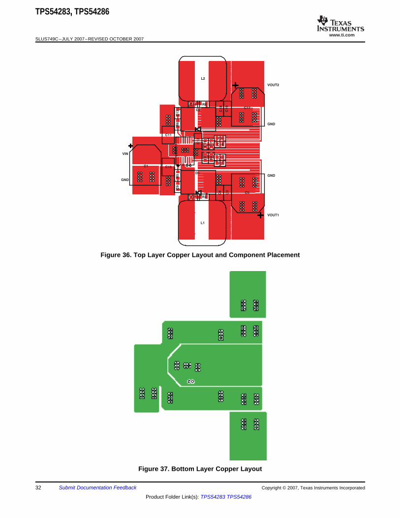
The layout guidelines presented here are illustrated in the printed circuit board layout example given in Figure 36and Figure 37.• The PowerPAD must be connected to a low current (signal) ground plane having a large copper surface area
to dissipate heat. Extend the copper surface well beyond the IC package area to maximize thermal transfer ofheat away from the IC.
• Connect the GND pin to the PowerPAD through a 10-mil (.010 in, or 0.0254 mm) wide trace.• Place the ceramic input capacitors close to PVDD1 and PVDD2; connect using short, wide traces.• Maintain a tight loop of wide traces from SW1 or SW2 through the switch node, inductor, output capacitor and
rectifier diode. Avoid using vias in this loop.• Use a wide ground connection from the input capacitor to the rectifier diode, placed as close to the power
path as possible. Placement directly under the diode and the switch node is recommended.• Locate the bootstrap capacitor close to the BOOT pin to minimize the gate drive loop.• Locate voltage setting resistors and any feedback components over the ground plane and away from the
switch node and the rectifier diode to input capacitor ground connection.• Locate snubber components (if used) close to the rectifier diode with minimal loop area.• Locate the BP bypass capacitor very close to the IC; a minimal loop area is recommended.• Locate the output ceramic capacitor close to the inductor output terminal between the inductor and any
Example 1: Detailed Design of a 12-V to 5-V and 3.3-V Converter
+
+
+
TPS54283,, TPS54286
SLUS749C–JULY 2007–REVISED OCTOBER 2007
The following example illustrates a design process and component selection for a 12-V to 5-V and 3.3-V dualnon-synchronous buck regulator using the TPS54283 converter. Design Example List of Materials and Table 4,Definition of Symbols is found at the end of this section.PARAMETER NOTES AND CONDITIONS MIN NOM MAX UNIT
INPUT CHARACTERISTICS
VIN Input voltage 6.9 12.0 13.2 V
IIN Input current VIN = nom, IOUT = max 1.6 2.0 A
No load input current VIN = nom, IOUT = 0 A 12 20 mA
OUTPUT CHARACTERISTICS
VOUT1 Output voltage 1 VIN = nom, IOUT = nom 4.8 5.0 5.2V
VOUT2 Output voltage 2 VIN = nom, IOUT = nom 3.2 3.3 3.4
Line regulation VIN = min to max 1%
Load regulation IOUT = min to max 1%
VOUT(ripple Output voltage ripple VIN = nom, IOUT = max 50 mVPP)
The first step is to estimate the duty cycle of each switching FET.
Using an assumed forward drop of 0.5 V for a schottky rectifier diode, the Channel 1 duty cycle is approximately40.1% (minimum) to 48.7% (maximum) while the Channel 2 duty cycle is approximately 27.7% (minimum) to32.2% (maximum).
The peak-to-peak ripple is limited to 30% of the maximum output current. This places the peak current farenough from the minimum overcurrent trip level to ensure reliable operation.
For both Channel 1 and Channel 2, the maximum inductor ripple current is 600 mA. The inductor size isestimated in Equation 23.
The next higher standard inductor value of 22 µH is used for both inductors.
The resulting ripple currents are :
Peak-to-peak ripple currents of 0.498 A and 0.416 A are estimated for Channel 1 and Channel 2 respectively.
The RMS current through an inductor is approximated by Equation 25.
and is approximately 2.0 A for both channels.
The peak inductor current is found using:
An inductor with a minimum RMS current rating of 2.0 A and minimum saturation current rating of 2.25 A isrequired. A Coilcraft MSS1278-223ML 22-µH, 6.8-A inductor is selected.
A schottky diode is selected as a rectifier diode for its low forward voltage drop. Allowing 20% over VIN forringing on the switch node, the required minimum reverse break-down voltage of the rectifier diode is:
The diode must have reverse breakdown voltage greater than 15.8 V, therefore a 20-V device is used.
The average current in the rectifier diode is estimated by Equation 28.
For this design, 1.2-A (average) and 2.25 A (peak) is estimated for Channel 1 and 1.5-A (average) and 2.21-A(peak) for Channel 2.
An MBRS320, 20-V, 3-A diode in an SMC package is selected for both channels. This diode has a forwardvoltage drop of 0.4 V at 2 A.
The power dissipation in the diode is estimated by Equation 29.
For this design, the full load power dissipation is estimated to be 480 mW in D1, and 580 mW in D2.
The TPS54283's internal compensation limits the selection of the output capacitors. From Figure 24, the internalcompensation has a double zero resonance at about 3 kHz. The output capacitor is selected by Equation 30.
Solving for COUT using• fRES = 3 kHz• L = 22 µH
The resulting is COUT = 128 µF. The output ripple voltage of the converter is composed of the ripple voltageacross the output capacitance and the ripple voltage across the ESR of the output capacitor. To find themaximum ESR allowable to meet the output ripple requirements the total ripple is partitioned, and the equationmanipulated to find the ESR.
Based on 128 µF of capacitance, 300-kHz switching frequency and 50-mV ripple voltage plus rounding up theripple current to 0.5 A, and the duty cycle to 50%, the capacitive portion of the ripple voltage is 6.5 mV, leaving amaximum allowable ESR of 87 mΩ.
To meet the ripple voltage requirements, a low-cost 100-µF electrolytic capacitor with 400 mΩ ESR (C5, C17)and two 10-µF ceramic capacitors (C3 and C4; and C18 and C19) with 2.5-mΩ ESR are selected. From thedatasheets for the ceramic capacitors, the parallel combination provides an impedance of 28 mΩ @ 300 kHz for14 mV of ripple.
The primary feedback divider resistors (R2, R9) from VOUT to FB should be between 10 kΩ and 50 kΩ tomaintain a balance between power dissipation and noise sensitivity. For this design, 20 kΩ is selected.
The lower resistors, R4 and R7 are found using the following equations.
• R2 = R9 = 20 kΩ• VFB = 0.80 V• R4= 3.80 kΩ (3.83 kΩ standard value is used)• R7= 6.40 kΩ (6.34 kΩ standard value is used)
Checking the ESR zero of the output capacitors:
• C = 100 µF• ESR = 400 mΩ• ESR(zero) = 3980 Hz
Since the ESR zero of the main output capacitor is less than 20 kHz, an R-C filter is added in parallel with R4and R7 to compensate for the electrolytic capacitors' ESR and add a zero about 40 kHz.
The TPS54283 datasheet recommends a minimum 10-µF ceramic input capacitor on each PVDD pin. Thesecapacitor must be capable of handling the RMS ripple current of the converter. The RMS current in the inputcapacitors is estimated by Equation 38.
• IRMS(CIN) = 0.43 A
One 1210 10-µF, 25 V, X5R ceramic capacitor with 2-mΩ ESR and a 2-A RMS current rating are selected foreach PVDD input. Higher voltage capacitors are selected to minimize capacitance loss at the DC bias voltage toensure the capacitors maintains sufficient capacitance at the working voltage.
To ensure proper charging of the high-side FET gate and limit the ripple voltage on the boost capacitor, a 33-nFboot strap capacitor is used.
Current limit must be set above the peak inductor current IL(peak). Comparing IL(peak) to the available minimumcurrent limits, ILIM is left floating for the highest current limit level.
The SEQ pin is left floating, leaving the enable pins to function independently. If the enable pins are tiedtogether, the two supplies start-up ratiometrically. Alternatively, SEQ could be connected to BP or GND toprovide sequential start-up.
The power dissipation in the TPS54283 is composed of FET conduction losses, switching losses and internalregulator losses. The RMS FET current is found using Equation 39.
This results in 1.05-A RMS for Channel 1 and 0.87-A RMS for Channel 2.
Conduction losses are estimated by:
Conduction losses of 198 mW and 136 mW are estimated for Channel 1 and Channel 2 respectively.
The switching losses are estimated in Equation 41.
From the data sheet of the MBRS320, the junction capacitance is 658 pF. Since this is large compared to theoutput capacitance of the TPS54x8x the FET capacitance is neglected, leaving switching losses of 17 mW foreach channel.
The regulator losses are estimated in Equation 42.
Table 4. Definition of SymbolsCDJ Average junction capacitance of the rectifier diode from 0V to VIN(max)COSS Average output capacitance of the switching MOSFET from 0V to VIN(max)COUT Output CapacitorD(max) Maximum steady state operating duty cycleD(min) Minimum steady state operating duty cycleESR(max) Maximum allowable output capacitor ESRfSW Switching frequencyIBP Output Current of BP regulator due to external loadsIDD Switching quiescent current with no load on BPID(avg) Average diode conduction currentID(peak) Peak diode conduction currentIIN(avg) Average input currentIIN(rms) Root mean squared (RMS) input currentIL(avg) Average inductor currentIL(rms) Root mean squared (RMS) inductor currentIL(peak) Peak current in inductorILRIP(max) Maximum allowable inductor ripple currentL(min) Minimum inductor value to maintain desired ripple currentIOUT(max) Maximum designed output currentIRMS(cin) Root mean squared (RMS) current through the input capacitorIRIPPLE Inductor peak to peak ripple currentIQSW(rms) Root mean squared current through the switching MOSFETPCON Power loss due to conduction through switching MOSFETPD(max) Maximum power dissipation in diodeRDS(on) Drain to source resistance of the switching MOSFET when “ON”PSW Power loss due to switchingPREG Power loss due to the internal regulatorVBP Output Voltage of BP regulatorV(BR)R(min) Minimum reverse breakdown voltage rating for rectifier diodeVFB Regulated feedback voltageVFD Forward voltage drop across rectifier diodeVIN Power stage input voltageVOUT Regulated output voltageVRIPPLE(cap) Peak to Peak ripple voltage due to ideal capacitor (ESR = 0 )VRIPPLE(tot) Maximum allowable peak to peak output ripple voltage
For a higher input voltage, both a snubber and bootstrap resistors are added to reduce ringing on the switchnode and a 30 V schottky diode is selected. A higher resistance feedback network is chosen for the 12 V outputto reduce the feedback current.
Figure 45. 24-V to 12-V and 24-V to 5-V Using the TPS54283
Figure 46. Switch Node Ringing Without Snubber and Figure 47. Switch Node Ringeing With Snubber andBoost Resistor Boost Resistor
For a low input voltage application, the TPS54286 is selected for reduced size and all ceramic output capacitorsare used. 22-µF input capacitors are selected to reduce input ripple and lead capacitors are placed in thefeedback to boost phase margin.
Figure 49. 5-V to 3.3V and 5-V to 1.2 V
Figure 50. Efficiency vs. Load Current Figure 51. Example 3 Loop Response
The following parts have characteristics similar to the TPS54283/6 and may be of interest.
Table 5. Devices Related to the TPS54283 and TPS54286TI LITERATURE DEVICE DESCRIPTIONNUMBER
SLUS642 TPS40222 5-V Input, 1.6-A Non-Synchronous Buck ConverterTPS54383 /SLUS774 3-A Dual Non-Synchronous Converter with Integrated High-Side MOSFETTPS54386
These references, design tools and links to additional references, including design software, may be found athttp:www.power.ti.com
Table 6. ReferencesTI LITERATURE DESCRIPTIONNUMBER
SLMA002 PowerPAD Thermally Enhanced Package Application ReportSLMA004 PowerPAD™ Made EasySLUP206 Under The Hood Of Low Voltage DC/DC Converters. SEM1500 Topic 5, 2002 Seminar SeriesSLVA057 Understanding Buck Power Stages in Switchmode Power SuppliesSLUP173 Designing Stable Control Loops. SEM 1400, 2001 Seminar Series
The following pages outline the mechanical dimensions of the 14-Pin PWP package and providerecommendations for PCB layout.
HPA00442PWP ACTIVE HTSSOP PWP 14 90 Green (RoHS& no Sb/Br)
CU NIPDAU Level-2-260C-1 YEAR -40 to 85 54286
HPA00443PWPR ACTIVE HTSSOP PWP 14 2000 Green (RoHS& no Sb/Br)
CU NIPDAU Level-2-260C-1 YEAR -40 to 85 54286
HPA00547PWPR ACTIVE HTSSOP PWP 14 2000 Green (RoHS& no Sb/Br)
CU NIPDAU Level-2-260C-1 YEAR -40 to 85 54286
TPS54283PWP ACTIVE HTSSOP PWP 14 90 Green (RoHS& no Sb/Br)
CU NIPDAU Level-2-260C-1 YEAR -40 to 85 54283
TPS54283PWPG4 ACTIVE HTSSOP PWP 14 90 Green (RoHS& no Sb/Br)
CU NIPDAU Level-2-260C-1 YEAR -40 to 85 54283
TPS54283PWPR ACTIVE HTSSOP PWP 14 2000 Green (RoHS& no Sb/Br)
CU NIPDAU Level-2-260C-1 YEAR -40 to 85 54283
TPS54283PWPRG4 ACTIVE HTSSOP PWP 14 2000 Green (RoHS& no Sb/Br)
CU NIPDAU Level-2-260C-1 YEAR -40 to 85 54283
TPS54286PWP ACTIVE HTSSOP PWP 14 90 Green (RoHS& no Sb/Br)
CU NIPDAU Level-2-260C-1 YEAR -40 to 85 54286
TPS54286PWPG4 ACTIVE HTSSOP PWP 14 90 Green (RoHS& no Sb/Br)
CU NIPDAU Level-2-260C-1 YEAR -40 to 85 54286
TPS54286PWPR ACTIVE HTSSOP PWP 14 2000 Green (RoHS& no Sb/Br)
CU NIPDAU Level-2-260C-1 YEAR -40 to 85 54286
TPS54286PWPRG4 ACTIVE HTSSOP PWP 14 2000 Green (RoHS& no Sb/Br)
CU NIPDAU Level-2-260C-1 YEAR -40 to 85 54286
(1) The marketing status values are defined as follows:ACTIVE: Product device recommended for new designs.LIFEBUY: TI has announced that the device will be discontinued, and a lifetime-buy period is in effect.NRND: Not recommended for new designs. Device is in production to support existing customers, but TI does not recommend using this part in a new design.PREVIEW: Device has been announced but is not in production. Samples may or may not be available.OBSOLETE: TI has discontinued the production of the device.
(2) Eco Plan - The planned eco-friendly classification: Pb-Free (RoHS), Pb-Free (RoHS Exempt), or Green (RoHS & no Sb/Br) - please check http://www.ti.com/productcontent for the latest availabilityinformation and additional product content details.TBD: The Pb-Free/Green conversion plan has not been defined.Pb-Free (RoHS): TI's terms "Lead-Free" or "Pb-Free" mean semiconductor products that are compatible with the current RoHS requirements for all 6 substances, including the requirement thatlead not exceed 0.1% by weight in homogeneous materials. Where designed to be soldered at high temperatures, TI Pb-Free products are suitable for use in specified lead-free processes.
Pb-Free (RoHS Exempt): This component has a RoHS exemption for either 1) lead-based flip-chip solder bumps used between the die and package, or 2) lead-based die adhesive used betweenthe die and leadframe. The component is otherwise considered Pb-Free (RoHS compatible) as defined above.Green (RoHS & no Sb/Br): TI defines "Green" to mean Pb-Free (RoHS compatible), and free of Bromine (Br) and Antimony (Sb) based flame retardants (Br or Sb do not exceed 0.1% by weightin homogeneous material)
(3) MSL, Peak Temp. - The Moisture Sensitivity Level rating according to the JEDEC industry standard classifications, and peak solder temperature.
(4) There may be additional marking, which relates to the logo, the lot trace code information, or the environmental category on the device.
(5) Multiple Device Markings will be inside parentheses. Only one Device Marking contained in parentheses and separated by a "~" will appear on a device. If a line is indented then it is a continuationof the previous line and the two combined represent the entire Device Marking for that device.
(6) Lead/Ball Finish - Orderable Devices may have multiple material finish options. Finish options are separated by a vertical ruled line. Lead/Ball Finish values may wrap to two lines if the finishvalue exceeds the maximum column width.
Important Information and Disclaimer:The information provided on this page represents TI's knowledge and belief as of the date that it is provided. TI bases its knowledge and belief on informationprovided by third parties, and makes no representation or warranty as to the accuracy of such information. Efforts are underway to better integrate information from third parties. TI has taken andcontinues to take reasonable steps to provide representative and accurate information but may not have conducted destructive testing or chemical analysis on incoming materials and chemicals.TI and TI suppliers consider certain information to be proprietary, and thus CAS numbers and other limited information may not be available for release.
In no event shall TI's liability arising out of such information exceed the total purchase price of the TI part(s) at issue in this document sold by TI to Customer on an annual basis.
Texas Instruments Incorporated (TI) reserves the right to make corrections, enhancements, improvements and other changes to itssemiconductor products and services per JESD46, latest issue, and to discontinue any product or service per JESD48, latest issue. Buyersshould obtain the latest relevant information before placing orders and should verify that such information is current and complete.TI’s published terms of sale for semiconductor products (http://www.ti.com/sc/docs/stdterms.htm) apply to the sale of packaged integratedcircuit products that TI has qualified and released to market. Additional terms may apply to the use or sale of other types of TI products andservices.Reproduction of significant portions of TI information in TI data sheets is permissible only if reproduction is without alteration and isaccompanied by all associated warranties, conditions, limitations, and notices. TI is not responsible or liable for such reproduceddocumentation. Information of third parties may be subject to additional restrictions. Resale of TI products or services with statementsdifferent from or beyond the parameters stated by TI for that product or service voids all express and any implied warranties for theassociated TI product or service and is an unfair and deceptive business practice. TI is not responsible or liable for any such statements.Buyers and others who are developing systems that incorporate TI products (collectively, “Designers”) understand and agree that Designersremain responsible for using their independent analysis, evaluation and judgment in designing their applications and that Designers havefull and exclusive responsibility to assure the safety of Designers' applications and compliance of their applications (and of all TI productsused in or for Designers’ applications) with all applicable regulations, laws and other applicable requirements. Designer represents that, withrespect to their applications, Designer has all the necessary expertise to create and implement safeguards that (1) anticipate dangerousconsequences of failures, (2) monitor failures and their consequences, and (3) lessen the likelihood of failures that might cause harm andtake appropriate actions. Designer agrees that prior to using or distributing any applications that include TI products, Designer willthoroughly test such applications and the functionality of such TI products as used in such applications.TI’s provision of technical, application or other design advice, quality characterization, reliability data or other services or information,including, but not limited to, reference designs and materials relating to evaluation modules, (collectively, “TI Resources”) are intended toassist designers who are developing applications that incorporate TI products; by downloading, accessing or using TI Resources in anyway, Designer (individually or, if Designer is acting on behalf of a company, Designer’s company) agrees to use any particular TI Resourcesolely for this purpose and subject to the terms of this Notice.TI’s provision of TI Resources does not expand or otherwise alter TI’s applicable published warranties or warranty disclaimers for TIproducts, and no additional obligations or liabilities arise from TI providing such TI Resources. TI reserves the right to make corrections,enhancements, improvements and other changes to its TI Resources. TI has not conducted any testing other than that specificallydescribed in the published documentation for a particular TI Resource.Designer is authorized to use, copy and modify any individual TI Resource only in connection with the development of applications thatinclude the TI product(s) identified in such TI Resource. NO OTHER LICENSE, EXPRESS OR IMPLIED, BY ESTOPPEL OR OTHERWISETO ANY OTHER TI INTELLECTUAL PROPERTY RIGHT, AND NO LICENSE TO ANY TECHNOLOGY OR INTELLECTUAL PROPERTYRIGHT OF TI OR ANY THIRD PARTY IS GRANTED HEREIN, including but not limited to any patent right, copyright, mask work right, orother intellectual property right relating to any combination, machine, or process in which TI products or services are used. Informationregarding or referencing third-party products or services does not constitute a license to use such products or services, or a warranty orendorsement thereof. Use of TI Resources may require a license from a third party under the patents or other intellectual property of thethird party, or a license from TI under the patents or other intellectual property of TI.TI RESOURCES ARE PROVIDED “AS IS” AND WITH ALL FAULTS. TI DISCLAIMS ALL OTHER WARRANTIES ORREPRESENTATIONS, EXPRESS OR IMPLIED, REGARDING RESOURCES OR USE THEREOF, INCLUDING BUT NOT LIMITED TOACCURACY OR COMPLETENESS, TITLE, ANY EPIDEMIC FAILURE WARRANTY AND ANY IMPLIED WARRANTIES OFMERCHANTABILITY, FITNESS FOR A PARTICULAR PURPOSE, AND NON-INFRINGEMENT OF ANY THIRD PARTY INTELLECTUALPROPERTY RIGHTS. TI SHALL NOT BE LIABLE FOR AND SHALL NOT DEFEND OR INDEMNIFY DESIGNER AGAINST ANY CLAIM,INCLUDING BUT NOT LIMITED TO ANY INFRINGEMENT CLAIM THAT RELATES TO OR IS BASED ON ANY COMBINATION OFPRODUCTS EVEN IF DESCRIBED IN TI RESOURCES OR OTHERWISE. IN NO EVENT SHALL TI BE LIABLE FOR ANY ACTUAL,DIRECT, SPECIAL, COLLATERAL, INDIRECT, PUNITIVE, INCIDENTAL, CONSEQUENTIAL OR EXEMPLARY DAMAGES INCONNECTION WITH OR ARISING OUT OF TI RESOURCES OR USE THEREOF, AND REGARDLESS OF WHETHER TI HAS BEENADVISED OF THE POSSIBILITY OF SUCH DAMAGES.Unless TI has explicitly designated an individual product as meeting the requirements of a particular industry standard (e.g., ISO/TS 16949and ISO 26262), TI is not responsible for any failure to meet such industry standard requirements.Where TI specifically promotes products as facilitating functional safety or as compliant with industry functional safety standards, suchproducts are intended to help enable customers to design and create their own applications that meet applicable functional safety standardsand requirements. Using products in an application does not by itself establish any safety features in the application. Designers mustensure compliance with safety-related requirements and standards applicable to their applications. Designer may not use any TI products inlife-critical medical equipment unless authorized officers of the parties have executed a special contract specifically governing such use.Life-critical medical equipment is medical equipment where failure of such equipment would cause serious bodily injury or death (e.g., lifesupport, pacemakers, defibrillators, heart pumps, neurostimulators, and implantables). Such equipment includes, without limitation, allmedical devices identified by the U.S. Food and Drug Administration as Class III devices and equivalent classifications outside the U.S.TI may expressly designate certain products as completing a particular qualification (e.g., Q100, Military Grade, or Enhanced Product).Designers agree that it has the necessary expertise to select the product with the appropriate qualification designation for their applicationsand that proper product selection is at Designers’ own risk. Designers are solely responsible for compliance with all legal and regulatoryrequirements in connection with such selection.Designer will fully indemnify TI and its representatives against any damages, costs, losses, and/or liabilities arising out of Designer’s non-compliance with the terms and provisions of this Notice.