INTERNATIONAL TECHNOLOGY ROADMAP FOR SEMICONDUCTORS 2009 EDITION RADIO FREQUENCY AND ANALOG/MIXED-SIGNAL TECHNOLOGIES FOR WIRELESS COMMUNICATIONS THE ITRS IS DEVISED AND INTENDED FOR TECHNOLOGY ASSESSMENT ONLY AND IS WITHOUT REGARD TO ANY COMMERCIAL CONSIDERATIONS PERTAINING TO INDIVIDUAL PRODUCTS OR EQUIPMENT. THE INTERNATIONAL TECHNOLOGY ROADMAP FOR SEMICONDUCTORS: 2009
Transcript
INTERNATIONAL
TECHNOLOGY ROADMAP FOR
SEMICONDUCTORS
2009 EDITION
RADIO FREQUENCY AND ANALOG/MIXED-SIGNAL TECHNOLOGIES
FOR WIRELESS COMMUNICATIONS
THE ITRS IS DEVISED AND INTENDED FOR TECHNOLOGY ASSESSMENT ONLY AND IS WITHOUT REGARD TO ANY COMMERCIAL CONSIDERATIONS PERTAINING TO INDIVIDUAL PRODUCTS OR EQUIPMENT.
THE INTERNATIONAL TECHNOLOGY ROADMAP FOR SEMICONDUCTORS: 2009
TABLE OF CONTENTS Radio Frequency and Analog/Mixed-signal Technologies for Wireless Communications .....1
Scope ..............................................................................................................................................1 RF and AMS CMOS.....................................................................................................................................3 RF and AMS Bipolar Devices.......................................................................................................................3 On- and Off-Chip Passives for RF and AMS................................................................................................4 Power Amplifiers (0.4 GHz–10 GHz) ...........................................................................................................4 Millimeter Wave (10 GHz–100 GHz)............................................................................................................5 MEMS...........................................................................................................................................................5
Difficult Challenges..........................................................................................................................6 RF and AMS CMOS.....................................................................................................................................6 RF and AMS Bipolar Devices.......................................................................................................................6 On- and Off-Chip Passives for RF and AMS................................................................................................7 Power Amplifiers (0.4 GHz–10 GHz) ...........................................................................................................8 Millimeter Wave (10 Ghz–100 Ghz) .............................................................................................................9 MEMS...........................................................................................................................................................9
Technology Requirements.............................................................................................................10 RF Figures of Merit ...................................................................................................................................10 Changes in the Technology Requirements Tables for 2009.................................................................10 RF and AMS CMOS..................................................................................................................................11 RF and AMS Bipolar Devices ..................................................................................................................11 On- and Off-Chip Passives for RF and AMS..........................................................................................12 Power Amplifiers (0.4 GHz–10 GHz) .........................................................................................................13 Millimeter Wave (10 GHz–100 GHz)..........................................................................................................16 MEMS.........................................................................................................................................................17
Potential Solutions.........................................................................................................................17 RF and AMS CMOS...................................................................................................................................17 RF and AMS Bipolar Devices.....................................................................................................................18 On- and Off-Chip Passives for RF and AMS..............................................................................................18 Power Amplifiers (0.4 GHz–10 GHz) .........................................................................................................20 Millimeter Wave (10 GHz–100 GHz)..........................................................................................................22 MEMS.........................................................................................................................................................23
More Than Moore – Heterogeneous Integration............................................................................26 References ....................................................................................................................................28
THE INTERNATIONAL TECHNOLOGY ROADMAP FOR SEMICONDUCTORS: 2009
LIST OF FIGURES Figure RFAMS1 Applications of RF and Analog/Mixed-Signal Technologies ...........................2 Figure RFAMS2 0.4 GHz–10 GHz Potential Solutions............................................................21 Figure RFAMS3 10 GHz–100 GHz Potential Solutions...........................................................25 Figure RFAMS4 Options for Increased Performance and Functionality ..................................26
LIST OF TABLES Table RFAMS1 RF and Analog Mixed-Signal CMOS Technology Requirements...................11 Table RFAMS2 RF and Analog Mixed-Signal Bipolar Technology Requirements ..................12 Table RFAMS3 On-Chip Passives Technology Requirements ...............................................13 Table RFAMS4 Off-chip Passives Technology Requirements ................................................13 Table RFAMS5 Power Amplifier Technology Requirements ...................................................15 Table RFAMS6 Base Station Devices Technology Requirements ..........................................15 Table RFAMS7 Millimeter Wave 10 GHz–100 GHz Technology Requirements .....................17 Table RFAMS8 RF and Analog Mixed-Signal RFMEMS.........................................................27
Link to 2009 ITRS Wireless Table file
THE INTERNATIONAL TECHNOLOGY ROADMAP FOR SEMICONDUCTORS: 2009
HRADIO FREQUENCY AND ANALOG/MIXED-SIGNAL TECHNOLOGIES FOR WIRELESS COMMUNICATIONS 1
RADIO FREQUENCY AND ANALOG/MIXED-SIGNAL TECHNOLOGIES FOR WIRELESS COMMUNICATIONS SCOPE Radio frequency and analog/mixed-signal (RF and AMS) technologies are essential and critical technologies for the rapidly growing wireless communications market. These technologies depend on many materials systems, some of which are compatible with complementary metal oxide semiconductor (CMOS) processing, such as SiGe and others of which may not be compatible with CMOS processing such as those compound semiconductors composed of elements from group III and V in the periodic table. Compound semiconductors become more significant as today’s emerging research devices, especially those devices based on the More than Moore (MtM) technologies described in this 2009 ITRS, are deployed in the marketplace.
The purposes of this 2009 ITRS RF and AMS chapter are as follows:
1. Present the challenges that RF and AMS technologies have in meeting the demands of wireless applications for cellular phones, wireless local area networks (WLANs), wireless personal area networks (WPAN), phased array RF systems, and other emerging wireless communication, radar, and imaging applications operating between typically 0.4 GHz and 100 GHz. We will be addressing applications beyond 100 GHz as they emerge in the marketplace.
2. Address the intersection of Si complementary oxide semiconductor (CMOS), BiCMOS (bipolar + CMOS), and SiGe heterojunction bipolar transistors (HBTs with III-V compound semiconductor devices.
This 2009 RF and AMS chapter presents the challenges, technology requirements, and potential solutions for the basic technology elements (transistors and passive devices) used in wireless communication front-end circuits. The chapter also maintains the applications driven perspective. This 2009 RF and AMS chapter has six main sections. The five sections on AMS CMOS, RF and AMS Bipolar Devices, On- and Off-Chip Passives for RF and AMS, Power Amplifiers (PAs), and micro-electro-mechanical systems (MEMS) cover primarily 0.4 GHz to 10 GHz application. The sixth section is on mm-wave technologies and covers 10 GHz to 100 GHz applications. Unlike in previous editions, we now treat the use of RF CMOS at frequencies greater than 10 GHz solely in the mm-wave tables. These frequencies refer to the nominal carrier frequencies for communications and are not necessarily the clock or operating frequencies of the individual devices and circuits. Even though the mm-wave spectrum starts pedagogically at 30 GHz, this section has been extended down to 10 GHz because the challenges, technical requirements, and technologies for the 10 GHz to 30 GHz spectrum are similar to those for the 30 GHz to 100 GHz spectrum. However, we note to the contrary that there are several companies that now apply analog design techniques traditionally used for low frequencies to applications in the mm-wave spectrum.
In addition to the six sections mentioned above, this chapter has a new section on "More than Moore- Heterogeneous Integration of Silicon and III-V Compound Semiconductors" that includes discussions on performance and costs.
The drivers for wireless communications systems are cost, frequency bands, power consumption, functionality, and size of mobile units, very high volumes of product, and standards and protocols. Also, RF technologies often require additional compromises with respect to performance parameters and figures of merit because several conflicting or competing requirements have to be met simultaneously. These include power added efficiency (PAE), high output power, low current, and low voltage. Increased RF performance for silicon is usually achieved by geometrical scaling. Increased RF performance for III-V compound semiconductors is achieved by optimizing carrier transport properties through materials and bandgap engineering. During the last two decades, technologies based on III-V compounds have established new business opportunities for the wireless communications industry. When high volumes of product are expected, silicon and silicon-germanium replace the III-Vs in those markets for which these group IVs can deliver appropriate performance at low cost.
The wireless communication circuits considered as application drivers for this roadmap may be classified into AMS circuits (including analog-to digital and digital-to analog converters), RF transceiver circuits (including low noise amplifiers (LNAs), frequency synthesizers, voltage-controlled oscillators (VCO), driver amplifiers and filters) and PAs.
THE INTERNATIONAL TECHNOLOGY ROADMAP FOR SEMICONDUCTORS: 2009
2 HRADIO FREQUENCY AND ANALOG/MIXED-SIGNAL TECHNOLOGIES FOR WIRELESS COMMUNICATIONS
Figure RFAMS1 Applications of RF and Analog/Mixed-Signal Technologies Figure RFAMS1 illustrates some examples of applications that span the frequencies and the technologies addressed in the chapter. Compared to the applications spectrum figure in the 2005 Roadmap, many of the materials and device technologies illustrated here have moved to higher frequencies and the upper bound of any technology’s applicability is not indicated.1 The consumer portions of wireless communications markets are very sensitive to cost and when multiple technologies are capable of achieving application specifications, many variables affect cost considerations. As a result, the choice of materials and device technologies among the different application cannot be definitively specified.
Compound III-V semiconductors had traditionally dominated the mm-wave spectrum over the past several decades. However, today, with the drive to low-cost and high-volume applications such as auto radar, along with scaling to sub-100 nm dimensions, the group IV semiconductors Si and SiGe have rapidly moved up to frequencies that were once the exclusive domain of the III-Vs. Several wireless applications and the materials and device technologies capable of addressing them are illustrated in Figure RFAMS1.
Metamorphic high electron mobility transistors (MHEMTs) may displace both GaAs pseudomorphic high electron mobility transistors (PHEMTs) and InP high electron mobility transistors (HEMTs) for certain applications. In fact, InP HEMTs and GaAs MHEMTs show promise well into the sub THz spectrum, which is beyond the scope of this roadmap. While the wide bandgap semiconductor GaN currently competes with silicon discrete laterally diffused metal oxide semiconductor (LDMOS) (Si-LDMOS) for infrastructure such as base stations at frequencies around 2 GHz, recent research papers suggest that GaN is capable of significant power and efficiency through 94 GHz, and perhaps even to 220 GHz, over the next few years. While Si-based technologies will prevail for high volume, cost sensitive markets in the mm-wave range, they are unlikely to replace III-Vs in applications where combinations of high power, high breakdown voltage, gain, and ultra low noise are required. Conversely, for low volume applications, III-Vs are likely to prevail due to the high initial costs in fabrication infrastructure [e.g., mask sets] for Si technologies.
The decisions on which materials and device technology performs best for a given application now depend more on key figures of merits such as such noise figure, output power, power added efficiency, and linearity than on frequency. Two or more technologies may coexist with one another for certain applications such as cellular transceivers, modules for terminal PAs, and mm-wave receivers. Today, BiCMOS in cellular transceivers has the biggest share in terms of volume compared to CMOS. But, the opposite may occur in the future as evident by the expanding wireless local area network (WLAN) connectivity market that is dominated by CMOS transceivers. Today, both GaAs HBT and LDMOS devices in modules for terminal power amplifiers have big market shares compared to GaAs PHEMTs and GaAs metal semiconductor field effect transistors (MESFETs) but these are being displaced by a maturing GaN technology. In the future, silicon-based technologies having higher integration capabilities will gain importance as systems require higher degrees of functionality. Today we see GaAs PHEMTs and InP HEMTs in mm-wave receivers. In the future, we may see
THE INTERNATIONAL TECHNOLOGY ROADMAP FOR SEMICONDUCTORS: 2009
HRADIO FREQUENCY AND ANALOG/MIXED-SIGNAL TECHNOLOGIES FOR WIRELESS COMMUNICATIONS 3
competition from SiGe (HBTs), GaAs MHEMTs, and GaN HEMTs and the heterogeneous integration of CMOS with III-V devices.
RF AND AMS CMOS The application drivers for the RF and AMS CMOS section are mobile transceivers in the 0.4 GHz – 10 GHz frequency range. The technology basis of this section has been and remains the CMOS devices in the low standby power (LSTP) roadmap of the Process Integration, Devices, and Structures (PIDS) chapter. The LSTP roadmap was selected as the basis for this section of the RF and AMS Roadmap because portable applications require lower standby power and higher bias voltages than high performance (HP) or low operating power (LOP) CMOS. The devices in this roadmap are assumed to be identical to those in the LSTP roadmap, but modifications may prove necessary if key analog properties cannot be realized. The devices are placed into production one year later than the LSTP roadmap to allow development of high-frequency models and other tools to support RF and AMS design. The focus is divided between two application areas. First, a performance-RF/analog device modeled after the LSTP device. Such devices are used in circuits for transceivers; frequency synthesizers, frequency converters and amplifiers. Then, there are supporting analog-specific applications requiring device characteristics that are difficult to achieve with scaled MOS or for driving RF signals off-chip which also requires higher voltage devices. Therefore, this section includes discussions on analog precision MOS device scaling, but with relatively high voltages to achieve high signal-to-noise ratios and low signal distortion. Such devices are typically available in CMOS technology offerings to support interfacing to higher-voltage input/output (I/O) ports, although many foundries also are including optional analog-friendly FETs as well. Furthermore, to support the even higher-voltage interfaces required by mobile devices (battery, display, etc.) optional high-voltage devices are often being included in CMOS technologies.
The millimeter-wave table for CMOS is in the millimeter-wave section of this chapter.
RF AND AMS BIPOLAR DEVICES Bipolar transistors covered by this roadmap are Si/SiGe heterojunction bipolar transistors (HBTs). The roadmap does not cover all types of Si/SiGe HBTs available in today’s technologies, but focuses only on those for which performance increases are driven by the wireless applications. Wireless transceiver applications in the 0.4 GHz to 10 GHz range continue to be the largest market for bipolar and BiCMOS technologies. However, wireless transceiver applications are no longer driving leading edge performance because existing SiGe NPN HBTs are sufficient for these frequencies. The scope of this section is then to provide requirements for high-speed NPN (HS-NPN), high-speed PNP (HS-PNP) and power-amplifier NPN (PA) HBTs.
The HS-NPN device is driven by the requirements of millimeter-wave products, e.g. 60 GHz WPAN, 77 GHz - 79 GHz automotive radar, 94 GHz imaging, 120 GHz to 160 GHz imaging, and gigabit Ethernet (40 Gb/s, 100Gb/s, and beyond) 2, 3. The HS-PNP device is driven by applications such applications as HDD, DVD/CD-R/W, thin-film transistor (TFT) displays, high resolution video, instrumentation and the like. Such applications require high performance analog and mixed-signal ICs. These ICs, such as drivers, video amplifiers, bus interfaces, DAC/ADC, and operational amplifiers, greatly benefit from complementary BiCMOS (C-BiCMOS) technologies that offer both NPN and PNP transistors with matched performances. Matching the performance of the NPN transistor is the aim of the HS-PNP roadmap. The PA-NPN device is driven by the requirements of power amplifiers of the RF transceiver modules for CDMA, WCDMA and GSM cellular handsets (i.e., operating frequencies between 900 MHz and 2 GHz).4, 5 Performances of PA HBTs are tied to the battery voltage and its evolution. Although a reduction in battery voltage is not foreseen today, the PA HBT roadmap anticipates these potential changes by providing device requirements for scaled breakdown voltage devices.
The years indicated in the bipolar roadmap are not the production-start year but rather the prototyping-start year. The life span of BiCMOS technologies (defined by length of time at a significant production volume) is much larger (~10 years) than that for CMOS technologies, because for a given application, they may not benefit much by simple (critical dimension) scaling. The end result is that BiCMOS technologies are not available for all the CMOS nodes. For these reasons, the roadmaps provided here do not attempt to tie bipolar performance to a given CMOS node. CMOS node choice depends on many factors, some of which are company specific: bipolar performance requirements, gate density requirements, process integration compatibility, development time, and cost. However, a year-by-year roadmap is kept to reflect the continued increase in bipolar performance as the applications involve higher operating frequencies.
Today, the most advanced BiCMOS technologies utilizing the HS-NPN offer 180 nm and 130 nm CMOS. This represents a three to four generation technology-node gap between advanced CMOS and BiCMOS technologies. This is explained by the lack of product drivers requiring dense digital functions, the cost advantages of integration on mature CMOS
THE INTERNATIONAL TECHNOLOGY ROADMAP FOR SEMICONDUCTORS: 2009
4 HRADIO FREQUENCY AND ANALOG/MIXED-SIGNAL TECHNOLOGIES FOR WIRELESS COMMUNICATIONS
nodes, and the ability to achieve excellent HS-NPN performance at these CMOS nodes. The 65 nm or 45 nm BiCMOS could appear in the coming years for mm-wave SOC applications that cannot be addressed by pure CMOS technologies. C-BiCMOS and PA-BiCMOS technologies usually lag behind HS-BiCMOS technologies with CMOS nodes ranging between 350 nm and 180 nm today. They indeed cover applications for which large gate densities are usually not required and for which cost is of primary importance.
ON- AND OFF-CHIP PASSIVES FOR RF AND AMS The scope of the on-chip passives section includes passive components used in RF and AMS circuits for wireless communications: 1) capacitors, 2) resistors, 3) inductors, 4) varactors, and 5) other passives for power amplifiers. Unlike digital CMOS circuits, the performance of many RF and AMS circuits are mainly determined by the performance of passive elements. Voltage and temperature coefficients are key parameters for capacitors and resistors. Also, capacitors and resistors are used in AMS circuits such as analog-to-digital and digital-to-analog converters that have clock frequencies below 0.4 GHz.
The passives section is expanded in the 2009 roadmap to include all technologies related to off-chip passives such as embedded passive devices that have growing applications in RF front-end modules, especially as the wireless market migrates to support multi-standard handsets. The scope of this section covers discrete components or chips integrated into package substrates to form passive devices. The substrates can be organic, such as printed circuit boards (PCBs) or in-organic, such as silicon or ceramic for both thick and thin film processes known either as multilayer substrate or high density interconnection (HDI) technology.
POWER AMPLIFIERS (0.4 GHZ–10 GHZ) Wireless communications require both portable and fixed transmitters and receivers to form a connected network. The public is most familiar with portable devices that take the form of cellular telephones and wireless personal digital appliances (PDAs). The scope of this section includes: III-V HBTs, Si metal oxide semiconductor field effect transistors (MOSFETs) and SiGe HBTs for terminal PAs. High voltage devices in base station power amplifiers, such as Si-LDMOS, and GaN FET, are also described in this Section. The key driving forces are integration of components and cost.
HANDSET POWER AMPLIFIER We will discuss first the power amplifiers (PAs) for the above portable devices. The PA in handheld devices is always a PA module (a multifunctional component that may contain a Si power management chip, RF matching networks, RF switches, and PA chips) capable of supplying 1-4 watts of RF power to the antenna of the portable device. Either Si CMOS or BiCMOS is typically used for power control circuitry (when there is no on-chip bias) and can also include the switch logic control functions. The RF matching components are used in the form of discrete components or custom integrated passive devices (IPDs) which are specially designed chips containing only passive elements in combination. These components are combined with transmission lines or passives embedded in a laminate structure to form the matching networks. GaAs PHEMTs and silicon on sapphire (SOS) CMOS are the most commonly used RF switch technologies. However, silicon on insulator (SOI) CMOS is recently becoming popular and getting significant traction. GaAs HBT, Si-LDMOS, SiGe HBT technologies are used for the power amplifier chips. Several components may be combined on the same semiconductor chip. A recent trend is to combine either the PA controller function with the switch function or the switch function with an IPD. Also, either the PA controller is integrated with PA on SiGe BiCMOS technology or the PA controller is integrated with the RF switch in SOS or SOI technology. Even some linear PAs are starting to include a CMOS-assist bias circuit to meet stringent current consumption vs. output power requirements. Combining several different PA module functions on a single chip reduces component count and wire bonding complexity and may lead lower cost modules. These technology combination approaches will become more prevalent as PA modules are required to service an increased number of frequencies and modulation formats in years to come. The choice of which technology to use for each function depends on the RF performance specifications, die size, availability, and most importantly total product cost.
BASE STATION POWER AMPLIFIERS The cellular base station, which also contains power amplifiers, completes the communications link between the portable device and the wire-line telephone network. Compared to handsets, however, substantially higher power RF devices up to 300 W are required to achieve the desired cellular phone coverage. A single base station may contain multiple of these 300 W devices to handle all of the cellular phone traffic at a particular base station site. Operating frequencies range between 400 MHz and 3.5 GHz. In recent years, worldwide interoperability for microwave access (WiMAX) appeared to
THE INTERNATIONAL TECHNOLOGY ROADMAP FOR SEMICONDUCTORS: 2009
HRADIO FREQUENCY AND ANALOG/MIXED-SIGNAL TECHNOLOGIES FOR WIRELESS COMMUNICATIONS 5
be on the verge of widespread deployment. But, that trend did not materialize. 4G deployments, on the other hand, are gaining markets by re-using frequencies between 700 MHz and 2.7 GHz.
The heart of base station transceiver is the RF semiconductor power device that must provide the final amplification to the data signal in order to achieve the desired output power. Typically, several semiconductor devices are connected in parallel to achieve these high powers. Silicon LDMOS transistors are now the technology of choice for cellular systems from 400 MHz through 3.5 GHz because of their combination of technological maturity, good performance, and low cost. The typical operating voltage of LDMOS devices is from 28V to 32V. The cost, performance, and reliability of LDMOS have created a value proposition with which GaAs PA devices have not kept up. Gallium nitride (GaN) continues to receive considerable attention as a potential next generation device technology. Gallium nitride has power densities four to five times greater than LDMOS. This tremendous increase in power density is the result of GaNs higher breakdown voltage and higher current density that offer many advantages to the PA design. Though GaN device development continues and the potential to increase efficiency is promising, the high cost and lack of maturity of GaN have prevented any significant deployment.
MILLIMETER WAVE (10 GHZ–100 GHZ) Commercial interest in the mm-wave spectrum has grown steadily over the past decade. Unlike most of the lower frequency spectrum, where silicon based technologies dominate, a number of distinct mm-wave semiconductor and device technologies compete in the applications marketplace. Each of these technologies offers unique tradeoffs in cost, performance, and availability. Currently, devices and integrated circuits are manufactured on four substrate materials: GaAs, InP, SiC, and Si. While the III-V compounds dominated the mm-wave spectrum a decade ago, Si-based device technologies now have crept into this applications arena, driven primarily by advantages in cost and integration level. For performance driven applications in which high levels of integration are needed, we expect a drive towards heterogeneous integration of III-V and silicon technologies. Such an approach would enable taking advantage of the high frequency performance of the III-Vs and the high density integration and processing capabilities of silicon. (See the More than Moore section in this chapter). In the future, we may see other III-V compound semiconductors, and even carbon-based semiconductors, including diamond and graphene, being developed for this spectrum (Refer to the Emerging Research Devices chapter).
In this section, we present transistor technologies which are, or are forecast to be, in commercial production for mm-wave applications in near-term years. Because this field is rapidly expanding, and because performance is not tied so tightly to lithographic dimensions as are digital integrated circuits, we have purposely omitted projections into the long-term years. Compound semiconductors do not enjoy the long-term heritage of silicon-based devices, nor do they follow Moore’s Law. As the mm-wave spectrum markets and products develop and become more of a technology driver, it may be more plausible to carry the roadmap for mm-waves into the long term for future ITRS editions.
The scope of this section includes low noise and power transistors that are based on the following materials and device technologies: GaAs PHEMT, GaAs MHEMT, InP HEMT, GaN HEMT, InP HBT, SiGe HBT and RF CMOS. Except for SiGe HBTs and RF CMOS, all device types employ epitaxial layers that are composed of ternary or quaternary compounds derived from column III and V of the periodic chart. There is great diversity in the nature and performance of these devices because device properties are critically dependent on the selection of materials, thickness, and doping in the epitaxial layers that are proprietary to the manufacturer. Trade-offs exist among power, efficiency, breakdown, noise figure (NF), linearity, and other performance parameters. One consequence of these trade-offs is that the “lithography roadmap” is not the primary driver for mm-wave performance, although lithography dimensions are certainly shrinking with the drive to high frequency figures of merit, such as maximum transit or cutoff frequency (fT) and maximum frequency of oscillation (fMAX). Performance trends are driven primarily by a combination of desirable trade-offs and “bandgap engineering” of the epitaxial layers in concert with shrinking lithography. In RF-CMOS, substrate orientation, bandgap engineering, gate stack engineering, and strain engineering have joined lithography as mm-wave performance drivers.
MEMS One of the emerging technologies to address needs in the consumer markets for wireless communication is micro-electrical mechanical systems (MEMS). MEMS have been around for a long time, e.g. used in mm-wave communications for antenna tuning, and are better know in the sensors and transducer application markets. Two examples of MEMS in high volume manufacturing are the Texas Instruments’ DLPTM technology for cinema projection and airbag sensors (accelerometers, produced by such companies as Analog Devices and Bosch) used in safety equipment in every car built today. Accelerometers are also the MEMS devices provided by Analog Devices and STMicroelectronics for the Nintendo
THE INTERNATIONAL TECHNOLOGY ROADMAP FOR SEMICONDUCTORS: 2009
6 HRADIO FREQUENCY AND ANALOG/MIXED-SIGNAL TECHNOLOGIES FOR WIRELESS COMMUNICATIONS
WiiTM. The unifying feature between all MEMS technologies are moving parts. However, the MEMS manufacturing technologies and approaches to provide solutions by MEMS are extremely diverse.
MEMS device usage is growing even more rapidly. MEMS enabled devices are now common for mobile and wireless communications applications. The scope for the 2009 MEMS roadmap includes the same four devices in the 2007 Roadmap [bulk acoustic wave (BAW) devices, resonators, capacitive switches, and metal contact switches], plus three new MEMS device types [sensors, microphones, and displays]. We discuss these three new MEMS device types in the test due to their increase use in RF and AMS products, but we do not include them in the roadmap tables.
In general, the four device types in Table RFAMS8 in the MEMS roadmap have found or will find their introduction into wireless communication products as discrete devices, e.g., a BAW filter mounted to a board or mother chip, or a Si MEMS oscillator replacing a quartz part in an existing socket. The performance of the MEMS discrete part is typically on par or better than the previous generation product (MEMS or non-MEMS) and its low cost allowed rapid adoption. For parts that have greater performance benefits, but no clear cost benefits, their introductions have been slowed in 2009 due to various economic factors and to technology maturity and demonstrated reliability of the existing part that the MEMS part would replace. .One example of the latter is the reliability of the packaged parts containing MEMS switches (capacitive and metal contact). In the cases where performance enabled new products with no significant cost barrier versus desired function of the product (e.g. MEMS microphones, MEMS accelerometers for handheld gaming and image rotation, and low end MEMS gyroscopes for navigation), market place introductions have been relatively rapid and assisted by use of existing, more mature MEMS process technology such as Si micromachining used in airbag sensors or inkjet printers.
The time at which the many and various MEMS devices are produced in high-volumes in the ITRS context will be when the MEMS function is integrated with the CMOS, BiCMOS, or bipolar semiconductor die. The timing for this integration will be primarily driven by cost. Until that time, initial introductions will occur in the following order: 1) favor discrete die (e.g. BAW devices), 2) above or below IC implementations (e.g. microphones/ variable capacitors), and 3) monolithic integrations with semiconductor die, which will potentially reduce the BOM by removing customized MEMS packaging from some devices and enable new applications due to integration and cost reduction.
DIFFICULT CHALLENGES RF AND AMS CMOS It is easy to assume that the steady improvement in the digital performance of the basic devices in the LSTP roadmap derived from scaling will also result in continuous improvement in RF and analog performance. But in fact, many of the dimensional, materials-oriented, and structural changes being invoked in the digital roadmap degrade or at least alter RF and analog device behavior. For example, it is well know that the halo or pocket implant degrades transistor gain even at long channel lengths.6 As dimensions shrink, new tradeoffs in physical design optimization for RF performance will be necessary as different mechanisms emerge as limiting factors determining parasitic impedances in local interconnects to the device.7 The introduction of new materials such as high-permittivity gate dielectrics, embedded structures to induce channel strain, and metal-gate electrodes makes predicting trends uncertain for transistor mismatch and for 1/f noise and, for now, the roadmap ignores any potential improvements or degradations from canonical scaling of these parameters.8,9 Eventually, as reflected in the LSTP roadmap, fundamental changes in device structures such as the introduction of multiple-gates and/or fully-depleted SOI will be required to sustain continued performance and density improvement. These structures prohibit a contact to the device body. Thus, the electrical characteristics of these devices are fundamentally different from those of conventional CMOS. Potential benefits include higher voltage-gain and lower coupling between the drain and body. But these differences, along with the steady reduction in supply voltages, pose significant circuit design challenges and may drive the need to make dramatic changes to existing design libraries. Thus, the fabrication of conventional precision analog / RF driver devices to be integrated alongside the scaled CMOS devices may require separate process steps. Even now, the impetus to enable system-on-chip (SOC) applications is encouraging the incorporation of optional analog or high-voltage devices and thereby expands the menu of potential devices albeit with the attendant cost increases.
RF AND AMS BIPOLAR DEVICES The primary challenge for the HS-NPN is increasing the unity current gain cut-off frequency fT by more aggressive vertical profiles while still maintaining low base resistance, manufacturing control, and punch-through margin. The second major challenge is handling the large current density and power density that result from the aggressive vertical
THE INTERNATIONAL TECHNOLOGY ROADMAP FOR SEMICONDUCTORS: 2009
HRADIO FREQUENCY AND ANALOG/MIXED-SIGNAL TECHNOLOGIES FOR WIRELESS COMMUNICATIONS 7
profiles. An additional challenge is the lower break-down voltage between the collector and emitter with the base open (BVCEO) of these devices, due to the high common-emitter current gain (β) and lower break-down voltage between the collector and base with the emitter open (BVCBO) that results from such aggressive vertical profiles. Although BVCEO does not limit maximum operating voltage, circuit operation above BVCEO places more demands on modeling device characteristics over many different regimes (e.g. negative base currents).
Similar to the HS-NPN, the main challenge for the HS-PNP is increasing fT by more aggressive vertical profiles. In addition to the inherent minority carrier mobility differences between electrons and holes, shrinking the vertical profile of a SiGe PNP is more challenging because it requires controlling the valence band offsets to avoid the appearance of parasitic barriers.
The major challenge for the PA is improving the tradeoff between the ratio fT/fMAX (where fMAX is the unity power gain maximum frequency of oscillation) .and breakdown voltages to provide voltage handling and power densities at performance levels that can effectively complete with alternative technologies.
ON- AND OFF-CHIP PASSIVES FOR RF AND AMS ON-CHIP PASSIVES Passive components include resistors, capacitors, inductors, varactors, transformers, and transmission lines. They are frequently used for impedance matching, resonance circuits, filters, and bias circuits in radio frequency integrated circuits (RFICs), such as LNAs, VCOs, mixers, and PAs. Even in some RF circuits, the performance of RF CMOS transistors is usually good enough for most of the applications well beyond 10 GHz. Therefore, the RF performance of passive devices always plays a key role in determining the overall characteristics of the entire circuit. For instance, integrating VCOs into RF transceivers with standard CMOS technologies is usually one of the most challenging design tasks, because there are many critical parameters that must be considered. Examples of such critical parameters are large frequency tuning range, low power consumption, and low phase noise. All these parameters are primarily determined by the passives used in VCO circuits (see also the AMS Section in the System Drivers chapter).
Integrating passives into RF chips is progressing in this era of SOC in order to realize high-performance low-cost RF CMOS technology, especially for some consumer electronics. When incorporating passives into a standard CMOS process, some additional photolithography and processing steps typically are needed. Moreover, new materials may be required for better passive performance. Therefore, tradeoffs between processing cost and device performance always exist. Nevertheless, this is quite a complex and application-dependent topic, because capacitors and inductors usually occupy much more Si area than active devices. Consequently, another optimization scheme should be implementing extra process steps or adding process complexity to increase the unit capacitance for smaller die size. Long-term challenges for passive elements will include the need to integrate new materials in a cost-effective manner to realize compact high quality factor (Q) inductors and high-density metal-insulator-metal (MIM) capacitors demanded by the roadmap.
OFF-CHIP PASSIVES Heterogeneous integration and system in a package (SIP) technology are widely applied to wireless communication portable devices. Selecting from among many packaging and assembly technologies the ones to use for a given RF and AMS circuit in a portable device presents challenges for designers of off-chip passives. In general, the IPD on a silicon substrate offers smallest size and highest precision. However, these devices also have higher substrate loss and higher cost that are the disadvantages for this method. Ceramic substrates usually provide low loss and high Q passives, but the variations and tolerances during the sintering process will cause mismatch and degrade circuit performance. Organic substrates such as PCB are the most cost effective and support a variety of different applications, but the loss, tolerance, and size make this approach still rarely used in mass production. The requirements for embedded components are similar to those of surface mount components. However, the process technology of the embedded components, the I/O interconnects and the process compatibility differs from those of surface mount components. Embedded passive device technology often involves additional materials such as high-k dielectrics for capacitors, resistive films or pastes for resistors, and high-permeability materials for inductors. These different materials may also require special processing. The large variation in embedded passives options increase complexity and cost. Accurate models, especially for process tolerance and parasitic effects, and computer assisted design (CAD) tools also are challenges when using these devices in RF and AMS circuits.
THE INTERNATIONAL TECHNOLOGY ROADMAP FOR SEMICONDUCTORS: 2009
8 HRADIO FREQUENCY AND ANALOG/MIXED-SIGNAL TECHNOLOGIES FOR WIRELESS COMMUNICATIONS
POWER AMPLIFIERS (0.4 GHZ–10 GHZ) HANDSET POWER AMPLIFIER The major challenge facing power amplifier devices and modules for portable communication devices is the need to increase their functionality in terms of operating frequency and modulation schemes while simultaneously meeting increasingly stringent linearity requirements at the same or lower cost. The consumer expects increasing portable device functionality without a substantial increase in portable device cost. Meeting these conflicting requirements is the biggest challenge facing the development of future PA modules. Some examples of recent customer requirements that impact technology choices are listed below.
For linear PAs used for such protocols as code division multiple access (CDMA), personal communications services (PCS), wideband CDMA (WCDMA) and the like, there is increasing focus on mid-power (16 dBm) efficiency. There are two popular solutions to this problem currently. The first is using a balanced architecture that requires no new process development. The second is including on-chip switching to by-pass one or all of the PA stages. This on-chip switching drives the integration of RF FETs and HBTs on the same die. More recently, such integration is being extended to have the efficiency measured at multiple power points which increases the complexity of the bias control and switching operations.
Load-insensitivity is another challenging requirement. Phone manufacturers are asking PA vendors to develop modules that are not sensitive to the load that the PA module sees. Previously, the major requirement was that the PA should be robust enough to withstand the voltage standing wave ratio (VSWR) when the isolator was removed. The current challenge is to meet performance specifications (e.g., noise figure, linearity, and PAE) over the same VSWR condition. The responses to this challenge will be varied and place differing demands on the selected technology.
Increasingly sophisticated bias circuits are being requested by PA users. Some examples of user requests include: 1) enable pins/mode control, 2) temperature compensation circuitry, 3) automatic bias control in which the PA senses power and resets bias based on the power it senses, and 4) circuits that do not require a reference supply voltage. The above request 3 may require integration of the power detector/coupler into the PA module. Also, using only npn transistors to meet the above request 4 is challenging. In general, the meeting the above requests or demands is the driver for BiFET integration where the FET is required to be a high quality analog FET. Continued emphasis on this area also makes BiCMOS, although it has RF shortcomings, an attractive alternative to GaAs HBT.
Enhanced data rates for global system for mobile (GSM) evolution (EDGE) PAs are typically integrated with GSM PAs, so there will be some convergence of the needs of linear PA and saturated PAs as PA designers must now provide linear operation as well. Some future modules may contain, not only the GSM-EDGE PA described above, but also long term evolution (LTE) and WCDMA – high speed packet access (HSPA) as well which will require more switching functions and possibly built-in load-tunability to minimize the number of required amplifiers while still maintaining specification compliance. LTE is a set of enhancements to the Universal Mobile Telecommunications System (UMTS) which will be introduced in the 3rd Generation Partnership Project (3GPP) Release 8. Much of 3GPP Release 8 will focus on adopting 4G mobile communications technology.
Another challenge that is presented to all handset PAs is the migration of battery technology. The likely near- term decrease in the end-of-life battery voltage presents a major technology and design challenge to PA vendors. This has huge implications for what has to happen at a system level. The PA will still need to work on a 4 V to 5 V charger, but also operate at lower voltages such as 2.4 V. Thereby, the operating range of the PA will increase. If the required output power remains unchanged, then some form of load-line switching will needed. Whether or not this is supplied by the phone manufacturer or the PA supplier will impact the choice of technology used. Another consequence will be that the transistors used in the power amplifier will be required to operate at a much higher current density to meet the same requirements and this will also have ramifications for which technologies can be used.
The incredible cost sensitivity and the fact that PAs tend to use a system-in-a-package (SIP) approach make the technology trends difficult to forecast.
BASE STATION POWER AMPLIFIERS One of the biggest challenges facing base station semiconductor technologies is the need for performance enhancements in the face of continual product price pressure. LDMOS technology, which owns over 95% of the base station market, has seen component costs drop from over a dollar per watt to less 30 cents per watt. The price differential between 1 and 2 GHz devices has also been diminishing. As cost continues to be squeezed out of the packaged device, we expect that the
THE INTERNATIONAL TECHNOLOGY ROADMAP FOR SEMICONDUCTORS: 2009
HRADIO FREQUENCY AND ANALOG/MIXED-SIGNAL TECHNOLOGIES FOR WIRELESS COMMUNICATIONS 9
price of the highest power parts will drop to the $0.15 per watt range within the next five years. Plastic packaging enables the most aggressive price points and continues to put downward pricing pressure on the more traditional ceramic packaged devices. We expect in the near future plastic packaged parts over 200 W and a clear trend to higher powers in plastic.
Improving amplifier efficiency is also a challenge for base station technology. This is primarily being addressed by exploring more efficient amplifier architectures: Doherty, drain modulation, and higher efficiency classes of operation (Class D, Class F, and Class S). Doherty amplifiers currently dominate high efficiency architecture deployment. We expect them to be the front runner for the next several years due to their maturity and relatively low incremental cost. These high efficiency architectures must continue to meet the stringent linearity performance requirements and cannot substantially increase system cost. Adaptive digital pre-distortion (DPD) designs where the input signal is pre-distorted in the digital domain to compensate for device non-linearities will help meet the linearity requirements. The adaptive behavior of the pre-distorter also mitigates issues with thermal time constants and device performance drift over time. GaN may offer advantages over LDMOS in certain classes of high efficiency architectures.
High efficiency architecture deployment represents an opportunity to design devices with attributes that are compatible with the architecture and can further enhance efficiency. For example, a Doherty-friendly device will have peak power and peak efficiency impedances designed to achieve maximum benefit from the load modulation that this architecture relies upon to improve efficiency without sacrificing peak power. The figures-of-merit that drive device development are a function of the PA architecture. Improving such figures of merit may potentially lead to devices that are designed for a specific PA architecture. That is, a device designed for use with a Doherty amplifier may not perform well in an input signal envelope tracking architecture. Understanding these figures-of-merit will enable device manufacturers to further enhance PA efficiency.
MILLIMETER WAVE (10 GHZ–100 GHZ) Compound semiconductor technologies have a number of similarities with silicon technologies and yet in many ways are distinctly different. While III-Vs have benefited from the advances in manufacturing equipment and chemistries, the development of these tools and chemicals is focused on the silicon industry and is not necessarily most favorable for compound semiconductor processing. Additionally, the need to thin wafers to 0.05 mm in thickness for thermal dissipation for GaAs and InP power devices and the more fragile nature of these substrates make wafer breakage a yield issue that is not problematic in silicon technologies
Semi-insulating GaAs wafers that are150 mm in diameter are routinely available and are becoming the de facto standard, although some foundries are still at 100 mm. The move to larger diameter substrates will be driven not only by economies of scale and chip cost but also by equipment availability. GaAs tends to be two generations behind Si in wafer size, with InP and SiC one and two generations, respectively, behind GaAs. It is crucial that substrate size keep up with Si advances if the III-V industry is to benefit from the advances in processing equipment. This continued pace in substrate size is particularly true for SiC, which still suffers from high defect density, although that is improving. Today there is no production source of semi-insulating GaN substrates. Most GaN device epitaxy relies on SiC for a host substrate and several firms now supply GaN epitaxial layers, tailored to customer specifications, on SiC substrates.
Device challenges, some of which are unique to III-Vs, include the following:
1. Efficient production techniques for fabrication of substrate vias required for low inductance grounds in microstrip mm-wave circuits;
2. Techniques for heat removal including wafer thinning and site specific cooling for high power density devices such as GaN;
3. High breakdown voltages for power devices and associated passive components such as capacitors; 4. Non-native oxide passivation and dielectric materials for mixed signal, enhancement/depletion (E/D) mode devices. 5. Reduction of leakage current and understanding of failure mechanisms, particularly for GaN materials which are
piezoelectric in nature.
MEMS The MEMS (micro-electrical mechanical systems) industry is not new and in many key ways differs from today’s semiconductor industry as best exemplified by CMOS manufacturing. With MEMS “one product, one process” has been the mantra and a new process may be required for a new product. As a result, there are several processes for many types of MEMS devices. This process diversity makes inclusion in specific ITRS process very challenging. For example, the
THE INTERNATIONAL TECHNOLOGY ROADMAP FOR SEMICONDUCTORS: 2009
10 HRADIO FREQUENCY AND ANALOG/MIXED-SIGNAL TECHNOLOGIES FOR WIRELESS COMMUNICATIONS
methods for producing a resonator can be as varied as wafer-to-wafer bonding of 3 wafers vs. monolithic integration of MEMS + CMOS using VLSI compatible thin film processes. And today, there is a wide variety of potential MEMS approaches for a given desired function, e.g. switch capacitor. To date, MEMS has entered the ITRS RF and AMS Roadmap due to (a) products already introduced to the marketplace, often as a disruptive rather than evolutionary technology, and (b) MEMS device performance, cost and design methodologies that have begun to be similar to those used in the general semiconductor industry and more specifically to those methodologies used in the commercial wireless communications products.
Two main factors will contribute to the widespread introduction of MEMS into today’s semiconductor markets and thus ITRS roadmapped products:
1. Foundries, in addition to independent device manufacturers (IDMs), and in particular “CMOS foundries,” start to offer MEMS unit modules and follow the foundry model. This has begun for the unit MEMS process and design modules integrated with other processes for high volume applications (e.g. MEMS + CMOS). The modules are reused for multiple designs and products.
2. More than performance is considered for each MEMS device type. To address the second point above and to aid the introduction of MEMS to semiconductor markets, the MEMS roadmap presents key needs from users for each selected MEMS device type. These needs have been separated into four sections: Design Tools, Packaging, Performance Driver, and Cost Driver. For the Packaging, Performance Driver, and Cost Driver sections, the goal is to treat each MEMS device type as one would treat a RF CMOS FET, an inductor, or circuit block, and to realize that high volume commercial opportunities are driven by a combination of performance, cost, and manufacturing complexity. For the Design Tools section, the goal is to recognize that integration of MEMS design tools with RF and AMS design flows can be central to rapid adoption of new MEMS applications and that design tool integration has not matured to levels similar to those for other RF/AMS design tools.
The table in this MEMS roadmap is less technically detailed than the others tables in the RF and AMS Roadmap, but the table reflects the complex emerging nature of MEMS solutions for RF and AMS products and the requirements for product introduction.
TECHNOLOGY REQUIREMENTS RF FIGURES OF MERIT Extracting reliable figures of merit (FOMs) from high frequency measurements becomes more difficult as device performance levels increase and parasitic resistances and capacitances are reduced. For this reason a sufficient device area is recommended to get capacitances exceeding a few tens of fF, which is a lower limit for reliable data. Measurement, de-embedding, and parameter extraction methodologies can have a significant impact on HF FOM. Although some complex procedures are developed to obtain the accuracy required for compact modeling, most companies utilize similar basic techniques to measure and monitor device cut-off frequencies.10, 11 The most common method used both for bipolar and field effect transistors is to utilize a two-dummy (Open + Short) de-embedding technique following a standard [short-open-load-through (SOLT) or line-reflect-reflect-match (LRRM)] impedance substrate standard (ISS) calibration. Even though the layout of these de-embedding structures and the precise de-embedding methodology may vary from one company to the other, the de-embedded device generally must keep the metal lines required to connect its electrodes , i.e., Metal 1 or Metal 1 + Metal 2 levels. This usually yields very repeatable results for unity current gain (h21) cut-off frequency, fT. For lower performance devices, like high-voltage and p-type devices, single-dummy (Open) de-embedding may be sufficient. The unity power gain maximum frequency of oscillation, fMAX, is extracted and reported from Mason’s gain (U) at a given frequency. However, the accuracy of this approach is the subject of much debate as this FOM is highly dependent on the cleanliness of the 20 dB/dec roll-off of U as a function of frequency. A conventional approach to verify fMAX is plotting fMAX = freq × √U, across a range of frequencies. This allows a reasonable estimate of fMAX if a constant value is obtained over a wide frequency range, while at the same time providing information on measurement error for fMAX.
CHANGES IN THE TECHNOLOGY REQUIREMENTS TABLES FOR 2009 Major changes for each of the first five sections in this chapter made since the 2008 updates in the Technology Requirements Tables are given here.
THE INTERNATIONAL TECHNOLOGY ROADMAP FOR SEMICONDUCTORS: 2009
HRADIO FREQUENCY AND ANALOG/MIXED-SIGNAL TECHNOLOGIES FOR WIRELESS COMMUNICATIONS 11
RF AND AMS CMOS There are few changes to the technology requirements roadmap beyond those resulting from the linkage to the LSTP roadmap. The trends of the LSTP and hence the RF and AMS CMOS roadmap to support higher integration and performance levels for logic with mixed-signal circuitry have continued albeit with the changes in scaling with time as reflected throughout the 2009 ITRS.
The increasing density of digital circuitry is the primary motivation for using advanced CMOS nodes to implement transceivers in the 0.4 GHz -10 GHz frequency range. Performance and cost considerations will continue to drive modularity of process features in order to adapt the technology to specific SOC architectures. However, the more stringent mixed-signal transistor requirements are forcing the addition of process complexity to achieve integration goals. The table notes that many foundries will offer optional devices to support precision analog applications or high-voltage applications as modular additions to the CMOS. These are relatively low-cost additions enabling greater on-chip functionality. CMOS technology is gaining importance in the field of mixed-signal to the detriment of bipolar and Si or SiGe-based BiCMOS processes. Technology requirements today are driven by the need for lower power consumption, lower noise, and lower cost in RF transceivers. Additional technology requirements will also be driven by the need to enable reconfiguring the RF transceiver in a software-defined radio and to enable higher level synthesis in RF transceivers (refer to the More-than-Moore discussion below). Emerging issues from this increased integration level are analog device modeling, protection against electrostatic discharge and optimization of physical design to minimize parasitic impedances as the underlying CMOS undergoes significant changes beyond geometry scaling. While the table reflects annual improvements in performance, following the LSTP roadmap, it is worth noting that foundries often provide RF and AMS support only at selected nodes and many application platforms will skip technology nodes when migrating to new product versions.
In one major change, the millimeter wave CMOS table has been moved to the millimeter-wave section of this chapter. The millimeter-wave CMOS entries were updated to be more consistent with the other devices tabulated by including peak transconductance as well as values at 24 GHz, 60 GHz, and 94 GHz for noise figure (NF) and maximum available gain (MAG).
Table RFAMS1 RF and Analog Mixed-Signal CMOS Technology Requirements
RF AND AMS BIPOLAR DEVICES The changes in the bipolar devices table are summarized as follows:
1. Dropped the high-voltage (HV) NPN because it is no longer driving the roadmap. This device is derived from the HS-NPN and is usually available by masking the selective collector implant (SIC). Although this device will likely remain available, its performance is strongly linked to that of the HS-NPN, with which it shares the same emitter/base construction and emitter/base doping profiles.
2. Introduced a roadmap for high-speed PNPs that limit the performance of existing C-BiCMOS applications. 3. Completed a major update of the HS-NPN roadmap to line up with the ongoing fT/fMAX trend, in line with
application requirements: a. Small change in fT leading to a lower fT compared to the previous roadmap for the 10 coming years. b. Included significant increase in the pace of fMAX change. fMAX increases much faster than fT. While the
focus of this device is on both high fT and fMAX, the new roadmap also focuses on a higher fMAX/fT ratio. c. Updated of all the other parameters accordingly. d. Added maximum available gain (MAG) at 60 GHz and 94 GHz whenever devices remain stable. e. Updated coloring
4. Updated PA device roadmap to anticipate a change in battery voltage: a. Included medium- and long-term changes to anticipate a change in battery voltage within 8 years. b. Reduced slightly for the short-term BVCEO; made no other short-term modifications. c. Reviewed breakdown voltages and cut-off frequencies accordingly. d. Separated emitter width (WE) of PA-NPN from WE of HS-NPN. e. Added maximum stable gain (MSG) at 900 MHz and 1.8 GHz. f. Updated coloring
THE INTERNATIONAL TECHNOLOGY ROADMAP FOR SEMICONDUCTORS: 2009
12 HRADIO FREQUENCY AND ANALOG/MIXED-SIGNAL TECHNOLOGIES FOR WIRELESS COMMUNICATIONS
Table RFAMS2 RF and Analog Mixed-Signal Bipolar Technology Requirements
ON- AND OFF-CHIP PASSIVES FOR RF AND AMS ON-CHIP PASSIVES The changes in the on-chip passives table are summarized as follows:
1. Continued table format with 3 applications: Analog, RF and Power Amplifier 2. Included the following four devices: Capacitors, Resistors, Inductors, and Varactors 3. Added metal-oxide-metal (MOM) interdigitated capacitor to RF capacitor
Analog MOS capacitors for decoupling are based on the roadmap specifications for the analog precision device in the CMOS tables. As the CMOS gate oxide thickness is being scaled, capacitor density increases but leakage current becomes an issue. In the year 2010, a gate oxide thickness of 3 nm is required. But, this thickness results in unacceptably high leakage currents and might require the use of high-κ dielectrics in the MOS capacitors to reduce the leakage current to acceptable levels.
Resistors are used in all analog and mixed signal circuit blocks. Highly-doped p-type polysilicon resistors are preferred in most cases for mixed-signal and analog applications due to their good matching, low parasitic capacitance to the substrate, and excellent temperature coefficient. These resistors consist of a polysilicon gate doped with a high-dose boron implant, which is normally the p-channel FET (PFET) source and drain (SD) implants. A 200–300 Ohm/square resistor is ideal for these applications. As CMOS is scaled further, the associated shallow and lower dose SD implants result in resistances that exceed 500 Ohm/square for these devices. This may require an additional mask for analog applications in the future and lower tolerance devices with smaller resistances. These devices have an excellent temperature coefficient that is less than 100 ppm/oC.
A thin-film back-end of line (BEOL) resistor has several attractive features such as low tolerance, low parasitics, and the ability to make design changes with short lead times. These are excellent for use in RF and analog applications, especially in I/O circuits and current biasing. A typical thin film resistor is comprised of TaN, a common material in the copper BEOL process. It is integrated above Metal 1 or other upper metallization levels and contacted with metal vias. These devices have excellent matching and are attractive for analog applications.
The key parameters for metal-insulator-metal (MIM) capacitors for RF applications are capacitance density, voltage linearity, leakage, matching, and Q factor. Higher capacitance density is required for capacitor area scaling. The matching tolerances become smaller as the capacitance area scales down. The capacitance density value in the table indicates the value for one capacitor and does not include the stacking of two capacitors on top each other that is sometimes done and requires doubling the mask levels and process steps. The value is for Cu back-end process that poses significantly more challenges compared to Al back-end in terms of integration and reliability.
Metal-Oxide-Metal (MOM) capacitors have the same key parameters as the MIM capacitors. The capacitance density of the MOM capacitors is determined by the width and space of multi level metal systems in the backend, and cannot be optimized independently of the back-end-system. Because the dimension control (space in particular) of the back-end-system is not as good as the control of the thin film thickness of the MIM capacitor, the matching of the MOM capacitors is usually significantly worse than that of the MIM capacitors.
The need for high performance on-chip monolithic spiral and multi-level spiral inductors in RF technologies recently has become increasingly important due to the technology and integration requirements of high functionality and low cost RF circuit applications. The typical interconnect scaling associated with digital circuit technologies, that is, BEOL scaling, is inconsistent with the need to keep series resistive losses low for high quality inductors. Additionally, minimizing substrate losses due to eddy currents and capacitive coupling is needed to increase Q. Integrating the inductors in the upper thick-metal levels of the BEOL and using large vias to provide a thick dielectric between the inductor and substrate help reduce these effects. Thick low-resistance metal wiring is needed for high Q applications such as in VCO circuits where high Q inductors are needed to reduce phase noise. Thick aluminum or copper inductors can be used to achieve peak Q performance of 25–30 for a 1 nH inductor at 3 GHz – 5 GHz.
Accumulation and depletion mode MOS varactors offer attractive tuning ranges and Q-factors. The requirements listed in the table are for MOS varactors based on gate oxide for performance RF/analog transistors. They are updated with respect
THE INTERNATIONAL TECHNOLOGY ROADMAP FOR SEMICONDUCTORS: 2009
HRADIO FREQUENCY AND ANALOG/MIXED-SIGNAL TECHNOLOGIES FOR WIRELESS COMMUNICATIONS 13
to the tuning range cited in the previous 2008 ITRS Update because higher tuning ranges have been achieved with the CMOS scaling. The continuous improvement in inductor Q-factors requires the varactor Q-factor to further increase, otherwise the varactor Q-factor becomes the limiting factor for VCO performance improvements. It is not clear to what extent varactors with additional gate length reductions can achieve the required Q-factors in the range of 50 and higher and how the varactor characteristics will be affected by the introduction of high-κ dielectrics.
OFF-CHIP PASSIVES The changes in the off-chip passives table are summarized as follows:
1. Changed the name of the table to reflect the growing importance of 3D integration and IPD. 2. Added three device elements for both organic and inorganic package substrate materials - resistors, capacitors
and inductors. 3. Included requirements for density, tolerance, temperature linearity, resonance frequency, and breakdown
voltage. Resistors will be required to support sheet resistances that range from 100 Ohm/square to 1K Ohm/square and will be extended to higher and lower sheet resistance values for both the thick and thin film processes. Temperature linearity is a key parameter for embedded resistors and must be less than 300ppm/ºC.
Precise control of capacitance to less than 1pF is required for matching circuits. The parallel plate Metal-Insulator-Metal (MIM) structure of embedded capacitors will be affected by the inter-layer misalignment especially as the capacitor area shrinks. High-k material is needed for increased capacitance density. For organic high-k material, the dielectric constant of about 50 is currently used in production, dielectric constant as high as 1000 will be needed for the future. As application frequency increases, the capacitor Q factor and self resonance frequency (SRF) will limit the high-k MIM capacitor performance. Low loss materials are also required for RF application. Smaller electrode sizes or special structures that minimize the parasitics of embedded capacitors will be needed to improve SRF performance.
The advantage for embedded inductor is high Q factor >40 and low process cost. The high-permeability material will become a key technology to increase the inductance density. Also, since the size of embedded inductors is relatively large, the coupled parasitic capacitance between wires will limit the SRF. Fine-line processes with either good process tolerances or special structures will be needed for the embedded inductors, especially as application frequency increases.
A need exists to manufacture by a roll-to-roll process future PCB embedded passives that have buried discrete component. Process control must be such that the untrimmed total tolerances including material and process are below 10% for capacitors and resistors and 5% for inductors.
POWER AMPLIFIERS (0.4 GHZ–10 GHZ) HANDSET POWER AMPLIFIER The changes in the handset power amplifier table are summarized as follows:
1. Added end-of-life battery voltage. 2. Added FET/HBT integration for integrated bias circuit design and on-chip switch integration for stage by-
passing. The trends in handset power amplifiers (PAs) respond directly to customer (phone manufacturers) demands and requirements, which are, in turn, driven by the desire to optimize the entire handset system. Optimizing the system leads to new technologies first being adopted at a power amplifier module (PAM) level that is integrated in the package. Package level integration can happen faster than new technology development for the system. However, system optimization may eventually be pushed back to the fundamental technology. Of course, since the life-span of a handset
THE INTERNATIONAL TECHNOLOGY ROADMAP FOR SEMICONDUCTORS: 2009
14 HRADIO FREQUENCY AND ANALOG/MIXED-SIGNAL TECHNOLOGIES FOR WIRELESS COMMUNICATIONS
model is approximately 18 months, time to market and lowest cost are always two of the top considerations in technology choice. There are four major trends that phone manufacturers will be driving.
1. The first is the use of battery technologies that have a lower end-of-life voltage than present systems have. This means that the PA will have to operate over a wider voltage range. Customer expectations for the low-end-voltage performance requirements have not been clearly defined. The specifications for low-end-voltage performance will determine the new technologies for load-switching and voltage control. The particular system partitioning that companies select will influence whether GaAs or silicon technologies are used. In addition, other technologies that provide a switching function will be needed at the module level.
2. A second trend, for linear handset applications such as CDMA, WCDMA, PCS, WiMAX, and LTE, is the requirement for greater functionality bias circuits to simplify system insertion and improve the mid-power efficiency at about 16 dBm. The more recent trend is to have multiple switching points. To meet these requirements, several companies have co-integrated FETs and HBTs in the same technology, similar to the BiFET process in silicon. This co-integration enables the following: 1) bias circuits to operate to lower reference voltages, 2) some flexibility in system insertion, 3) no reference voltages in some cases, and 4) some shut-off switching function on the bias circuit. Customers have requested all of these features. Implementing such features and applications requires a high-quality analog FET as given in Table RFAMS1. Stage by-passing is another application that requires FET-HBT co-integration. In this case, the FET must be a higher quality RF FET because it performs a RF switching function. The integration and refinement of FET-HBT technologies will certainly continue in the next few years. Finally, the implementation of “CMOS assisted” PAs is also being used to address need.
3. The emergence of “ultra low cost” markets is driving increasing interest and development activities in Si CMOS PAs that leverage the low cost and high integration in silicon. Although the power efficiency is still 5 % to 10 % behind of that in GaAs HBT PA, CMOS PA products have gained momentum and increasing market share in low-end GSM markets in India and China. The sale of these CMOS PAs has reached over 60 M chips annually. The distributed amplifier architecture with on-chip transformers (DAT) has been one of the widely adopted topologies for saturated PAs to deal with the low breakdown voltages (VGS and VDS) in CMOS FET devices. The performance improvement in linear PAs for CDMA and WCDMA is also being made by novel architectures in CMOS PA design, together with potential system solutions such as digital pre-distortion techniques. While the emphasis on CMOS PA design is currently on design and architecture, it may drive new technology requirements as co-integration of functions becomes more necessary.
4. Finally, in the next several years, there will be an increasing trend to integrate more bands and more modes onto a power amplifier module (PAM). One of the interesting questions is whether or not wireless-LAN will be included in this integration. This question is important because wireless-LAN PAs use predominantly SiGe or GaAs at 2.4 GHz and GaAs at 5.8 GHz. Recently dual band WLAN PAs (2.4 GHz and 5.8 GHz) in one SiGe chip, and their matching passives in one IPD chip have been reported.12 As these PAs are inserted into the system, new technology requirements might arise. A greater number of bands and modes also has an impact on switch technology used for PAMs. The linearity or isolation requirement can be very stringent on the RF switch, filter, and diplexer if we start to integrate 3 G or 4 G cellular modes and bands and many other functionalities such as a digital mobile TV tuner, global position system, and RF identification (RFID) in the phones. In order to save board real estate, it is desirable to have the switch logic controller directly integrated with the switch. Such integration reduces the number of bond pads and routing traces. This makes E/D PHEMT, SOS, and SOI, attractive contenders for switch technologies. The integrated antenna switch and GSM PA in SOS with competitive performance has recently emerged. The SOI RF switch has relatively lower cost compared with SOS due to the substrate difference. The integration of multi- band and multi-mode PAs will also drive the need for output match tunability in addition to just switching functions so that the module performance can be better optimized with a minimum number of actual amplification chains.
We also updated the PA passive values. The decision of product designers on where to put output matching components for the PA will drive the requirements for the passives. Currently, most PAMs are using either embedded passives or SMT components that can be selected with the best performance/cost trade-off. Placing some of these components on the PA will require MMICs to have similar precision and performance. Inductors are examples of this real world consideration where excellent Q values can already be obtained, but where the layout area required does not make sense from a cost standpoint. Removing the gold interconnect as some GaAs fabs have done also can reduce costs.
THE INTERNATIONAL TECHNOLOGY ROADMAP FOR SEMICONDUCTORS: 2009
HRADIO FREQUENCY AND ANALOG/MIXED-SIGNAL TECHNOLOGIES FOR WIRELESS COMMUNICATIONS 15
Table RFAMS5 Power Amplifier Technology Requirements BASE STATION POWER AMPLIFIER The changes in the base station power amplifier table are summarized as follows:
1. Covered cellular frequencies from 400 MHz to 2.7 GHz 2. Removed GaAs technology from the base station table because of the increased focus on GaN technology which
provides superior RF performance in terms of frequency, power density, and total RF power. 3. Revised key figures of merit to reflect impact of transition to high efficiency architectures
Cost pressures continue unabated. The transition to plastic encapsulated RF packages will continue and be extended to higher RF powers. The ability to remove cost from plastic packages is limited, which is expected to result in a reduction in the slope of the cost versus time curve. Cost differentials for higher frequencies are also diminishing.
The largest trend to emerge over the past two years has been the rapid deployment of Doherty amplifier techniques to enhance backoff performance. This trend is expected to continue over the next several years as device designers optimize the device characteristics to enhance Doherty performance, and as PA manufacturers extend the basic symmetrical Doherty architecture to include other techniques to boost performance, such as asymmetrical Doherty, and gate and/or drain bias modulation. Improvements in DPD linearization techniques are also likely to boost Doherty efficiency. The increased focus on Doherty is likely to keep this architecture as the dominant driver of base stations that require backed-off linear efficiency for the coming 3 to 5 years. It is not clear what architecture will replace Doherty, though drain modulation / envelope tracking and switch mode PAs are certainly possibilities.
The key device figures-of-merit (FOM) have also been evolving to align with the PA architecture; today’s dominant PA architecture for backed-off linear efficiency is Doherty. We revised accordingly the chart to include power density, low output capacitance, cascaded 1dB compression point (P1dB) efficiency, and linearized efficiency at 8dB output back-off (OBO), amongst others. We removed other FOMs such as 2-tone linear power and efficiency because they are less relevant now. We expect to revise the FOMs in this table as the limits of Doherty amplifier are reached in the coming years and the architecture required to meet the 8dB OBO linear efficiency target evolves.
Another trend that has emerged is the redeployment of existing frequency bands for next generation, high data rate wireless standards [i.e., fourth generation (4G) / LTE]. WiMAX at 3.5 GHz appears to be a niche that is not finding widespread deployment opportunities. The highest frequency for widespread 4Gdeployments appears to be 2.7 GHz, keeping the frequency of operation in a regime where LDMOS performance is competitive with GaN; the superior high frequency performance of GaAs and GaN technologies is only readily apparent at frequencies of 3.5 GHz and higher. The focus on linear efficiency rather than frequency response will extend the useful life of silicon-based LDMOS.
The interest in GaN HFET technology continues for both commercial and military applications. US government funding for the technology continues to be strong and is driving all aspects of the technology toward manufacturability. Commercial products are available from several companies. The advantage of GaN technology is its substantially higher RF power density which comes in part by its higher operating voltage (48 V). This coupled with a higher device current density enables power densities 4 to 5 times that of LDMOS. This high power density reduces the complexity of passive matching circuits which in turn reduces power loss in the amplifiers. However, this technological advantage comes at a higher device cost which will slow adoption of the GaN in commercial applications.
We removed in this 2009 chapter GaAs PHEMT technology because of its inability to successfully compete against the LDMOS in this market. The lack of a proven, robust, and reliable 28 V GaAs technology has enabled LDMOS to dominate the base station PA market, with GaAs devices never achieving a market share greater than the low single digits. Many GaAs suppliers also are exploring GaN technology due to the similarities in the manufacturing flows. Compared to GaAs, GaN offers the potential for a paradigm shift in PA design and performance, and hence is garnering the investment that used to flow to high voltage GaAs.
Table RFAMS6 Base Station Devices Technology Requirements
THE INTERNATIONAL TECHNOLOGY ROADMAP FOR SEMICONDUCTORS: 2009
16 HRADIO FREQUENCY AND ANALOG/MIXED-SIGNAL TECHNOLOGIES FOR WIRELESS COMMUNICATIONS
MILLIMETER WAVE (10 GHZ–100 GHZ) The changes in the millimeter wave table are summarized as follows:
1. Removed the peak current at fT (Imax) from low noise devices as it is not a factor which drives device designs or applications
2. Added MAG [Maximum Available Gain] predictions at 60 GHz and 94 GHz to SiGe HBT table 3. Moved mm-Wave GaN Power HMET production out to 2010
The mm-wave tables show a projection of both key parameters intrinsic to the device such as breakdown voltage, maximum current, and transconductance, as well as performance factors for low noise and power transistors at fixed frequencies, namely, noise measure, power, gain, and efficiency. We present predicted performance data at three frequencies of commercial interest across the 10 GHz to 100 GHz frequency spectrum: 24 GHz, 60 GHz, and 94 GHz. The 24 GHz spectrum is being positioned for wireless LAN applications and is being considered for automobile radar, although most of auto radar work has been done at 77 GHz. The 60 GHz frequencies, long used by the military for secure satellite cross links, falls in a region where atmospheric absorption is high, and as a consequence is ideal for short range, “last mile” connectivity in congested areas, where the short range facilitates frequency re-use. Within the near term scope of this roadmap, we expect to see applications opening at 94 GHz such as concealed weapons detection and imaging all weather aircraft landing systems. If we had we included long term projections past 2018, we would have incorporated device projections up to 220 GHz for imaging applications that are currently at the research and development stage and even up to frequencies in the sub-THz region. The spectrum from 100 GHz to 1000 GHz holds promise for many applications in the areas of medical imaging, spectroscopy, and security. The mm-wave Technology Requirements Section summarizes the diverse technology choices for the frequencies, 24 GHz, 60 GHz, and 94 GHz.
A review of the tables shows that no one material or device technology has the monopoly at any frequency. The user has many choices. We have made no attempt to select a preferred component for any particular application, because the choice can be driven by many factors, not the least of which is cost. Other factors are integration level, reliability heritage, operating voltage, and of course, performance, which is the focus of the roadmap. We have, however, made implicit predictions regarding the obsolescence and preferences for certain technologies. These predictions are implied by the “white space” [absence of parameters] in the out years for a particular technology, and are summarized below:
• We removed GaAs MESFETs from the mm-wave tables in 2007. Although high-voltage GaAs MESFETs may have a role under 10 GHz, we still see no new designs forthcoming for mm-wave applications due to superior performance along with cost and reliability parity of GaAs PHEMT technologies.
• Likewise, PHEMTs are likely to eventually give way to InP HEMTs and GaAs MHEMTs, although we foresee GaAs PHEMTs will remain into the next decade while costs remain competitive vs. alternative technologies
• Millimeter-wave power devices will fall into two regions: low power [a few to tens of watts] dominated in the near term by GaAs PHEMT and MHEMT, and high power [tens to hundreds of watts] dominated by GaN. We predict that GaN will replace GaAs power MHEMT by 2013.
• GaN may also have a niche in the low noise area for applications requiring high robustness and linearity. GaN noise measure is comparable to PHEMT, and because limiters can be eliminated from the front end of receivers, GaN devices will offer distinct advantages in system noise figure.
• InP, SiGe HBTs, and RF CMOS will continue to compete for applications. CMOS and SiGe offer clear cost and integration level advantages, while for equivalent lithography, InP may offer up to 4X improvement in performance.
RF CMOS was introduced to the mm-Wave Section in 2007. The CMOS table includes RF characteristics of CMOS devices in the high performance (HP) roadmap of the Process Integration, Devices, and Structures (PIDS) chapter. These devices are expected to be placed into production two years after the digital roadmap to allow for development of high-frequency models and design tools necessary to support the design of millimeter wave applications. The HP roadmap was selected as the basis for this table assuming early designers would select the inherent higher performance of the aggressively scaled CMOS. Later, the LSTP roadmap may be adopted as designer confidence grows or mobile applications emerge and require lower standby power. The low values of maximum allowed voltage of HP CMOS limits its usefulness in driving power. Therefore, power and efficiency are not considered in the table. The already low and shrinking supply voltage and correspondingly low maximum-allowed voltage of the HP CMOS roadmap will drive innovative design techniques and new circuit topologies. To address designs in the higher mm-wave frequency range,
THE INTERNATIONAL TECHNOLOGY ROADMAP FOR SEMICONDUCTORS: 2009
HRADIO FREQUENCY AND ANALOG/MIXED-SIGNAL TECHNOLOGIES FOR WIRELESS COMMUNICATIONS 17
minimum gate length transistors will likely be used to provide the device maximum bandwidth. These problems are not specific to CMOS or to mm-waves. In fact several groups have demonstrated reliable +10dBm CMOS PAs at 60 GHz with sub 1V supplies.13 and references therein The tradeoff between fT and breakdown and reliability is also true for SiGe, InP HBTs and even GaN HEMTs, albeit at different fT*BV products.
MEMS A MEMS table was included in the RF and AMS Roadmap in 2007 and in the 2008 Update. The few selected MEMS devices were RF and AMS in nature and were those that may improve or extend performance or reduce the cost and bill of materials of traditional RF and AMS electronics such as power amplifiers and transceivers.
The primary change to 2009 Roadmap involves the timing of potential solutions introduction to the marketplace due to economic factors in addition to technical maturity. In addition, more detail has been added to the Design Tools portion of the Roadmap to reflect the current trajectory of MEMS design tools and to break out device design from TCAD like process design tools.
Other changes include the following:
Design Tools
1. Separated Design tools into device design and TCAD like process simulators. 2. Moved out tool introduction for IRFM - integrated RF + mechanical 3D simulation due to difficulty (red). 3. Emphasized MEMS parametric-cell (P-cell) enabled RF and AMS design flow (red). 4. Inserted “foundry design flow” that emphasizes design kit enabled RF and AMS design flow (red).
Performance Driver
1. Moved out by one year the manufacturable known solutions for resonator high frequency and multi frequency devices (yellow).
2. Moved out by one year the manufacturable known solutions for capacitive contact switches (yellow). 3. Moved out by two years the manufacturable known solutions for metal contact switches due primarily to
reliability challenges (yellow). Cost Driver
1. Moved out by one year the manufacturable known solutions for resonator high frequency and multi frequency due to the cost of one die solution vs. 2 die solution. (red)
2. Moved out by two years the manufacturable known solutions for metal contact switches due primarily to the costs of the test to access package reliability. (yellow)
POTENTIAL SOLUTIONS The 2009 potential solutions tables are divided into two main tables: one covering the 0.4 GHz–10 GHz applications and one covering 10 GHz–100 GHz mm-wave applications.
RF AND AMS CMOS The CMOS solutions for mixed-signal applications differ from those already given for memory and logic applications discussed in sections of the Process Integration, Devices, and Structures (PIDS) chapter. Increased CMOS digital performance indeed results in an aggressive roadmap for NF, fT, and fMAX improvements. These figures of merit indicate a level of performance already well beyond what is necessary to implement conventional transceiver architectures in the 0.8 GHz – 20 GHz frequency range. This level of performance comes, however, with limited voltage-tolerance reflected in the Table RFAMS1. One direction for potential solutions is the development of new transceiver or circuit-block architectures, for example the use of power-combining techniques, to exploit the digital device properties. To continue using conventional analog architectures, successful mixed-signal technologies will leverage the baseline digital platform while integrating value-added features and functions. Key ingredients to successful mixed-signal integration are the
THE INTERNATIONAL TECHNOLOGY ROADMAP FOR SEMICONDUCTORS: 2009
18 HRADIO FREQUENCY AND ANALOG/MIXED-SIGNAL TECHNOLOGIES FOR WIRELESS COMMUNICATIONS
addition of special higher-voltage and analog precision transistors, high quality passive elements, adequate signal isolation, and compatible active devices. Implementing these features in a low-cost fashion will require innovation as the materials and structural configuration of CMOS technology evolves.
In addition to the obvious benefits of increased performance with scaling, technology changes may improve other device characteristics important to RF and analog circuit functions. The introduction of metal gates should reduce threshold mismatch due to variations in gate doping and increase fMAX due to decreased gate resistance. The introduction of channel strain to increase device current should enable improvements in precision analog and RF driver performance with little or no degradation in other characteristics. Fully-depleted, dual-gate SOI that has low channel doping relative to conventional CMOS structures is also expected to reduce mismatch. In addition, this structure will offer reduced drain conductance with an attendant increase in voltage-gain and fMAX. However, the introduction of metal gate electrodes, high permittivity gate dielectrics, and fully depleted, dual-gate SOI will pose additional challenges for mixed-signal applications. With the use of these technology elements, heretofore unimportant physical mechanisms may emerge as limiting factors of performance and will require reconsideration of physical and manufacturing practices. A full characterization and modeling of the RF properties and performance-limiting factors is necessary for effective implementation of mixed-signal applications.
The mixed-signal supply voltage continues to lag that of high-performance digital by two or more generations. A combination of multiple gate oxide thickness, multiple thresholds, and DC-DC conversion is needed to support the increased mixed-signal requirements. The added process complexity will be in contradiction to desired low cost. Design solutions in active threshold regulation, substrate biasing, and novel architectures will be required to extend the trend for lower supply voltages to mixed-signal applications.
Increasing integration levels drives the requirement for improved signal isolation and better simulation capability of cross-talk between circuit blocks. The use of high-resistivity silicon substrates will be required in the most demanding applications. An alternative to full integration is the SIP that combines circuits made with different technologies and optimized for the desired functions.
RF AND AMS BIPOLAR DEVICES Potential solutions for continuing to improve the fMAX of bipolar transistors (all types) include lithography advancements which help drive lateral device scaling to reduce parasitic device resistances and capacitances. This enables narrower emitter widths for reduced base resistance (RB), as well as reduces the unit length current at peak fT. The improved fMAX and reduced unit length current at peak fT can be traded-off for more aggressive vertical profiles (thinner base width and higher collector doping concentration) to drive fT increases while remaining within reliability limits for current handling in the metal interconnects. The improved fT and fMAX will also improve the noise figure at high frequency to address mm-wave requirements.
Control of the vertical profile may limit this approach. Potential solutions include the reduction of the process thermal budget by leveraging advanced CMOS solutions, such as spike or flash anneals, laser annealing, and reduced thermal budget silicide modules. Dopant profile control can be improved by the introduction of new deposition techniques. Potentially, new materials could help improve the transit time and/or control of the base width as the introduction of germanium or carbon did in the recent past.
Parasitic losses can significantly limit performance gains. Scaling of the intrinsic collector doping and extrinsic base doping profiles to drive fT and RB (fMAX) improvements leads to continued pressure on the CJC-RB trade-off. Potential solutions here include innovative architectures that further minimize the interaction between the extrinsic and intrinsic regions of devices, such as the introduction of selective epitaxy and self-aligned structures did in the past.
Potential solutions for addressing the BVCEO reduction include new emitter process modules designed to increase base current, and thus reduce common-emitter gain (β). It is important to notice that the BVCEO’s reported in the Bipolar Technology Requirements table do not anticipate the introduction of such modules.
ON- AND OFF-CHIP PASSIVES FOR RF AND AMS ON-CHIP PASSIVES The trend of moving discrete passive elements from board level to chip level will continue. Solutions for achieving discrete-equivalent precision on-chip passive components are expected. Alternatively, some passives may be integrated into the printed board or package as a method of cost reduction and simplification. New high-k dielectrics can be used either to reduce integrated capacitor area or to keep the integrated capacitor area acceptable for new emerging analog and
THE INTERNATIONAL TECHNOLOGY ROADMAP FOR SEMICONDUCTORS: 2009
HRADIO FREQUENCY AND ANALOG/MIXED-SIGNAL TECHNOLOGIES FOR WIRELESS COMMUNICATIONS 19
RF circuit functions. The high-k dielectrics can significantly increase the capacitance density of the MIM capacitor, MOS capacitor, and MOS varactor. The continued improvement and performance verification in linearity and matching of metal-oxide-metal (MOM) capacitor will make it an attractive low cost option for future analog and RF circuits.
Higher quality and higher density inductors can enable new functionality and circuit topology integrated on-chip and represent a significant challenge for analog and RF integrated circuits. Potential solutions for higher quality and higher density inductors include the use of thicker layers of Cu and thicker top dielectrics and the integration of magnetic materials with on-chip inductors. These may co-exist with inductors integrated in the package for the most demanding applications. Integrated resistors need low parasitic capacitance and high temperature linearity, which can be fulfilled by innovative approaches in fabrication of the integrated resistors.
Additional research is needed in the following two areas: 1) MOS capacitors and MOS varactors processed with high-k dielectrics. - coupled to the availability of high-k dielectrics, respectively, for analog high precision transistors and high-speed RF transistors; and 2) the impact on the VCO phase noise of the high-k dielectric, which typically has a much higher trap density.
In order to achieve high capacitance density for RF MIM capacitors, various high-k dielectrics are being explored. This includes Ta2O5, HfO2, and other high-k materials.
The key challenge is to keep the leakage current and voltage linearity low as the film thickness is reduced. One way to solve this tradeoff is to use multi-layered structures where the capacitance density and voltage linearity can be separately optimized. Whether such solutions are production worthy needs to be determined.
When feature size is scaled down and when the stacking structure or the high-k dielectric MIM is excluded, the unit capacitance of the inter-digitated, lateral MOM capacitor can be close to or exceed that of the standard MIM capacitor. Compared with the MIM capacitor, there are no additional processing steps and cost for the inter-digitated MOM capacitor. Therefore, it is recognized as a capacitor option, especially for low-cost applications. There are tradeoffs observed between the unit capacitance and the parasitic coupling with the Si substrate. Moreover, the mismatching performance of the inter-digitated MOM capacitor can’t be over-emphasized. However, the mismatching performance of the inter-digitated MOM capacitor can be competitive to that of the MIM capacitor by using proper structure designs.
Above-passivation inductors offer high Q-factors and resonance frequencies, but require special processing. Technical feasibility has been demonstrated. Some companies have this available as a production process. The choice whether to use above-passivation inductors depends on the limited access today to such technology and the economics. The latter is assessed on a case-by-case basis. Improvements in inductance density are difficult to realize. Solutions of stacking inductors have been proposed, but add significantly to the cost and jeopardize the resonance frequency due to the high capacitive coupling between the stacked inductors. The use of magnetic materials has received some attention in the literature, such as the use of magnetic shields. However, the research in this area is not yet complete.
Increasing CMOS complexity makes it more difficult to produce stable, highly manufacturable front-end-of-line (FEOL) resistors. One solution to this problem is to provide high-resistance BEOL resistors comparable to the common p-type polysilicon resistors in the FEOL. Due to thermal affects, this can be a problem because thermal control of these devices is paramount in the BEOL to minimize electromigration. This problem needs to be addressed with new materials that provide not only good resistor parametrics for RF and analog circuits but good thermal control at high currents. This is a good area for R&D on RF and analog technologies.
OFF-CHIP PASSIVES Embedded passives, including integrated passives devices (IPDs) and low temperature co-fired ceramic (LTCC) provide off-chip and inter-chip solutions for passive networks in circuit design. This technology is not only complementary to on-chip passives, but also provides packaging and interconnection solutions for the system. Process technologies for manufacturing passive components in the substrate, especially for organic PCBs, are divided in two major categories, lamination and printing. For the printing process, general screen printing is the most cost effective but less accurate. New process technology such as ink-jet printing provides a solution for improved process tolerance.
In general, even though the design, material, and process of organic embedded passives are different from silicon based technology, many concepts are similar. Another solution that is used increasingly is directly burying the surface mounted components into the substrate. This approach can minimize the tolerance of the components during PCB process and prevent testing difficulty of an embedded device that achieves high performance at low cost.
THE INTERNATIONAL TECHNOLOGY ROADMAP FOR SEMICONDUCTORS: 2009
20 HRADIO FREQUENCY AND ANALOG/MIXED-SIGNAL TECHNOLOGIES FOR WIRELESS COMMUNICATIONS
POWER AMPLIFIERS (0.4 GHZ–10 GHZ) HANDSET POWER AMPLIFIERS Integrated HBT-HEMT technologies will address several of the issues that power amplifier designers will face in the long and short terms. The integration of the FET with the HBT allows more complex bias circuits to be designed and integrated with the power chain. Such FET-HBT circuits also will allow integration stage by-passing switches to be place directly on the PA die and will contribute to improved mid-power efficiency. While these technologies are available now on a limited basis, manufacturing challenges will need to be addressed before these solutions become pervasive. While it is possible to fabricate circuits that perform these functions in BiCMOS, the RF gain for the high-bands still require improvement. One of the most important short-comings for Si(Ge) BiCMOS to become more widely used in handset PAs is the gain at higher frequencies great than 1.9 GHz. There are a number of technology advantages that GaAs HBT PA designers enjoy, compared to their silicon counterparts, which have nothing to do with the transistor. First, GaAs wafers are typically thinned to102 to 127 micrometers and include a through-wafer-via (TWV). The reduced emitter inductance by using TWVs has led to direct improvement in the PA gain. Thinning the wafer (as done for GaAs or silicon base-station applications) shortens the wire bonds and reduces the keep-out region around the die. Doing this reduces the package dimensions. Replacing bond-pads with TWV connections to ground reduces pad count and the die size (e.g. removing pads labeled GND). TWV provides a more consistent inductance and reduces product variation. Finally, using the TWV for grounding enables excellent thermal contact of the die with the package, compared to flip-chip solder bumps.
In silicon, TWV is also often referred as through silicon via (TSV). The TSV has been a very active area of development in SiGe PA technology. TSVs have been demonstrated successfully on silicon14, but have not yet made their way into high-volume production. The addition of TWV may help alleviate the RF gain problem that currently plaques Si(Ge) for higher frequency applications without adding extra stages. It may also pave the way for higher level integration of multi-mode multi-band PAs in one silicon chip.
The reduction of the end-of-life battery voltage will drive several possible solutions that depend on the type of PA being designed and the, as yet, undisclosed customer expectations on performance. Several technologies [MEMS, tunable varactors (using materials such as barium strontium titantate), or high-Q varactor networks] for varying or switching the load to the PA exist. These technologies will play significant roles in addressing the challenging end-of-life battery voltage issue. Such tunable networks will be required to improve performance over the entire PA operating range and which one(s) become the “right” solution(s) will depend heavily on cost structure and integrability into power amplifier modules (PAMs). Another potential solution for the battery voltage will be the use of DC to DC converters to adjust the supply voltage of the PA for different operating conditions. Whether these are provided in the phone as a signal from a different part of the handset or required inside the actual PA module will drive the architecture first and then if integration is required may drive technology.
MEMS deployment in PA and other RF applications has been delayed by about two years due to the recent economic downturn. Although MEMS have many advantages in delivering superior raw RF performances in linearity, insertion loss and isolation, it will still take a few years for MEMS to become compelling performance/cost/size tunable solutions. MEMS process integrations into the top foundry silicon technologies and strong adoption by some first tier phone manufacturers are two key factors that must occur. The solid state solutions with variable capacitors used for system tunability have also made progress and are closing the gap with MEMS.
THE INTERNATIONAL TECHNOLOGY ROADMAP FOR SEMICONDUCTORS: 2009
HRADIO FREQUENCY AND ANALOG/MIXED-SIGNAL TECHNOLOGIES FOR WIRELESS COMMUNICATIONS 21
First Year of IC Production 2009 2010 2011 2012 2013 2014 2015 2016 2017 2018 2019 2020 2021 2022 2023 2024
RF & AMS CMOSsub-10GHz tranceivers utilizing sub-1V digital cmos transistors
Full understanding and modeling of RF/Analog properties of FD-SOI or DG CMOS
Integration of high-voltage and analog devices with FD-SOI or DG CMOS
Integration of high-resistivity substrates into AMS CMOS technologies
SiGe BiCMOS
Si/SiGe:C Conventional CVD
New Materials and/or Advanced Deposition Techniques for Base Epitaxy
Annealing Techniques
Conventional Self-Aligned E/B Structure
Advanced Fully Self-Aligned E/B/C Architectures
Low-b Emitter Process Module
POWER AMPLIFIERS (Base stations)
28V LDMOS
48V LDMOS
GaN HFET Technology
High Voltage GaAs HBT
High Efficiency Amplifier Classes (D, E, S)
Passive DevicesHigher Dk dielectric material/Thinner dielctric thickness for decouple capacitor
High-μ material for high value inductor (analog or power circuit/device)
CAD tool for 3D SiP
Fuctional device design standard
This legend indicates the time during which research, development, and qualification/pre-production should be taking place for the solution. Research RequiredDevelopment UnderwayQualification / Pre-ProductionContinuous Improvement
Figure RFAMS2 0.4 GHz–10 GHz Potential Solutions
THE INTERNATIONAL TECHNOLOGY ROADMAP FOR SEMICONDUCTORS: 2009
22 HRADIO FREQUENCY AND ANALOG/MIXED-SIGNAL TECHNOLOGIES FOR WIRELESS COMMUNICATIONS
BASE STATION POWER AMPLIFIERS The trend towards re-using frequencies up to 2.7 GHz is likely to extend 32 V LDMOS dominance of the base station PA market by at least several years. Advanced Doherty architectures and the compatibility of LDMOS with Doherty will enable LDMOS to continue to offer competitive performance, especially given the cost advantage of LDMOS over alternative technologies such as GaN. GaN technology, on the other hand, offers compelling advantages in terms of the potential for improved efficiency, lower capacitance per watt, higher bandwidth, higher terminal impedance, ease of scaling to high power levels, and high frequency compatibility whenever frequencies eventually head higher. The GaN challenge in the short term is to demonstrate reliability on par with LDMOS, while more fundamentally the long term challenge is cost: GaN existing in more than niche markets requires a PA architecture that is enabled by GaN with an efficiency boost to offset the inherent higher cost of the GaN transistors. While GaN may offer improved Doherty performance compared to LDMOS, the performance delta is not expected to offset the cost premium associated with GaN devices. Other high efficiency PA architectures such as switch mode PAs, if enabled by GaN, may offer a more attractive performance / cost solution and create an opening for GaN to be successful in this market. GaN continues to benefit from military interest and funding, which will continue to drive reliability and performance improvements and keep GaN positioned as a viable next generation PA device technology.
Other technologies that may disrupt the status quo include 48 V LDMOS, and high voltage HBTs. 48 V LDMOS offers improvements in power density, impedance levels, scaling to high power, and lower capacitance per watt. But to date, they have lagged 32 V LDMOS technology by a few points in efficiency and have therefore not found widespread acceptance in the base station PA market. 48 V LDMOS device performance continues to improve, and may yet penetrate the base station PA market. High voltage HBTs have also been reported that offer impressive drain modulation and Doherty PA performance. On the other hand, ruggedness has always been the Achilles heel of bipolar transistors in general, and HBTs in particular. Improving the ruggedness without degrading the gain and frequency response can be challenging. If solutions to these problems can be found, HV HBTs could also become a viable challenger to LDMOS.
MILLIMETER WAVE (10 GHZ–100 GHZ) Compound semiconductors take advantage of the advances in lithography and processing equipment that are available in the silicon industry. In order to accomplish this, wafer diameters need to be within one or two generations of the silicon industry. Semi-insulating GaAs wafers that are 150 mm in diameter are in production now while InP wafers seem stalled at 100 mm for the foreseeable future. Silicon carbide semi-insulating substrates, the basis for GaN HEMTs, are at 100 mm. The III–V industry needs to continually push to larger wafer sizes to keep pace with the silicon equipment infrastructure. Advances in the growth of GaN on silicon can provide a viable path to 150 and 200 mm substrates.
While significant advances are being made in optical lithography tools, the cost of masks to define sub 0.25 micrometer features is prohibitive for most of the relatively low volume III-V applications. Direct-write electron beam is a solution to the mask cost, but wafer through-put, which is measured in hours per III-V wafer as compared to silicon wafers per hour, needs to be increased with high current electron sources and fast alignment systems.
Uniformity, reproducibility, and yield metrics for compound semiconductors still lag behind Si-based technologies. This is not surprising, given the much higher investment in infrastructure and research for silicon, as well as the extremely large disparity in production volume between the two. Nevertheless, as production volume in a particular compound technology rises, unit costs are found to decrease on a learning curve not unlike that of silicon.
Substrate quality is still problematic for the emerging wide bandgap devices, although quality has improved significantly over the past several years. Research on GaN templates is continuing, even though SiC substrates have become more viable as their defect density decreases. Thermal dissipation is the major challenge for wide-bandgap III-V power devices. While GaN and SiC substrates have higher thermal conductance values compared to GaAs and InP, the 5× to 10× higher power densities typically present in these wide bandgap semiconductors somewhat offset the advantage in higher thermal conductance. These circumstances make thermal dissipation a critical device design aspect. Proven techniques include thin 0.05 mm wafers, thermal shunts, and bathtub vias. These techniques and more innovative solutions such as diamond composites need to be applied to the wide bandgap devices.
Gate recessing for GaAs and InP based power FETs has been used successfully to achieve higher breakdown voltages. This approach is currently under development for GaN. In the meantime, use of field plates to tailor the electric field on the drain side of the gate has been effective in achieving high breakdown voltages, although this can compromise high frequency performance. Continued improvement of passivation and hot carrier effects is also needed.
THE INTERNATIONAL TECHNOLOGY ROADMAP FOR SEMICONDUCTORS: 2009
HRADIO FREQUENCY AND ANALOG/MIXED-SIGNAL TECHNOLOGIES FOR WIRELESS COMMUNICATIONS 23
High-voltage breakdown is desirable for both mixed-signal and high-power devices. In addition to transistor speed, for many mixed-signal or analog applications, breakdown voltage values of transistors greatly restrict the dynamic range of the circuits and represent a severe limitation. In this regard, InP HBTs offer a distinct advantage over SiGe HBTs, although the integration level offered by SiGe will be orders of magnitude greater. Careful device scaling and wide-bandgap collectors can help maintain breakdown in InP HBTs. Gallium nitride HEMTs offer even higher promise due to the potential for a 10x increase in the Johnson figure of merit [fT x breakdown voltage].
It is highly desirable in mixed signal electronics to have transistors capable of accommodating voltage swings of 10 V or more. The performance of other RF circuit elements, such as mixers, can be also directly related to the dynamic range of the device. Therefore, it is necessary to scale the dimensions of a transistor to achieve the desired frequency performance while maintaining desirable breakdown voltage to allow large voltage swing for high dynamic range.
Currently, the GaN technology is primarily driven by microwave frequency power amplifier applications due to its ultra high breakdown field. The cut-off frequencies of GaN field effect transistors are about 100 GHz and existing monolithic microwave integrated circuits (MMICs) only consists of no more than ten transistors with air-bridge interconnect system. Both the transistor performance and integration level of circuits are too low to enable high-performance mixed signal circuits. To fully exploit the potential of GaN devices for desired wide dynamic range circuits, a next-generation nitride electronic technology must be developed to achieve high transistor speed (~ 500 GHz) and high integration level (> 1000 transistors) by scaling the transistors, reducing parasitic resistances and capacitances, and utilizing multi-level interconnects as has been done in silicon technology. In addition, the development of a stable enhancement mode (E-mode) operation will be critical. This will offer many important practical advantages in circuit applications, including greater simplicity in mixed-signal and RF circuits and the ability to implement enhancement/depletion (E/D) logic capability (direct-coupled FET logic). Further, large scale integration of hundreds to thousands of transistors demands a manufacturing technology that can achieve high yield.
Uniformity of transistors is particularly important for mixed-signal electronics and further underscores the need to develop a robust, manufacturable device process. The impact of the future GaN technology will be profound and will, lead to dramatic improvements in the performance of RF and mixed-signal electronic circuits, which include high-speed high power amplifiers, ultra-linear mixers, and high-output-power digital-to-analog converters.
Finally, high frequency performance in III-Vs and now even in CMOS is driven as much by epitaxy, bandgap and strain engineering (vertical scaling), as by lithography (horizontal scaling). Carrier velocity and mobility in the transport layer can be tailored by properly engineering the epitaxial layer stack, the source and drain regions, the substrate orientation, and/or the dielectric stack above the device. We expect continued improvements by bandgap and strain engineering in all of the III-Vs and in MOS devices beyond the 32nm node.
MEMS In 2009, the primary business and market factors that will affect the future roadmap for MEMS integration into RF and AMS wireless communication systems included:
• Large increase in number MEMS fabs with 200 mm capability, in particular for foundry manufacturers. • Increased membership in MEMS Industry groups (e.g. MIG) conference topic inclusion. • An increasing number of proposed solutions that involve integration of the MEMS device directly into an existing
CMOS production line and layer stack, in particular for switches. • A well publicized increasing use of MEMS in mature mobile or wireless products (mature as defined by 2nd or 3rd
generation products or very high volume). Two examples are WII gaming accelerometers and iPhone display image rotation.
• A new interest in the 200 mm tool industry for MEMS from existing semiconductor tool suppliers due to semiconductor industry macroeconomic conditions for 200 mm fabs, slowdown in 300 mm tool sales, and search for new markets.
• The above business and market trends will drive down cost for new technology by achieving higher yield in more modern “ULSI” fabs, and lower the baseline cost due to the greater numbers of die per wafer. In addition, MEMS development announced at multiple CMOS fabs, and 200 mm wafer equipment investments at existing 150 mm wafer MEMS fabs, may assist the “integration with semiconductor die” portion of Table RFAMS8 in the Cost Driver section.
THE INTERNATIONAL TECHNOLOGY ROADMAP FOR SEMICONDUCTORS: 2009
24 HRADIO FREQUENCY AND ANALOG/MIXED-SIGNAL TECHNOLOGIES FOR WIRELESS COMMUNICATIONS
Technical factors for the device types reported in Table RFAMS8 include:
• Resonators (Si MEMS oscillators) have been introduced into the market as discrete components, but the monolithically integrated or higher / multi-frequency per die solutions for filtering applications central to RF and AMS products still require work on performance, e.g., frequency variation, and cost vs. other solutions. Quartz timing devices which have been adopted to offset the MEMS Si-based introduction and size advantage are among the other solutions in the industry standard.
• The reliability of the metal-metal interface for metal contact switches and their associated packaged parts as well as methods for low cost integration in consumer applications still remain key challenges. There is much work on materials innovation and system integration to accommodate existing material solutions. Also, competitive solutions made from solid-state device switches (e.g., LDMOS or FETs on SOI) are in production and offer adequate cost vs. performance and are mature compared to MEMS solutions.
• Capacitive switches are finding many potential applications, but MEMS reliability delays product introduction and packaging schemes still make cost a challenge for all but the highest volume or highest performance products.
• BAW filter advancements in part size reduction, e.g., though packaging, has helped cost and applicability for ever smaller consumer product introduction.
THE INTERNATIONAL TECHNOLOGY ROADMAP FOR SEMICONDUCTORS: 2009
HRADIO FREQUENCY AND ANALOG/MIXED-SIGNAL TECHNOLOGIES FOR WIRELESS COMMUNICATIONS 25
First Year of IC Production 2009 2010 2011 2012 2013 2014 2015 2016 2017 2018
mm-wave
Efficient substrate via production
Site specific cooling
Enhancement mode devices
Larger diameter, semi-insulating substrates
8" GaAs
6" SiC
4" InP
4" GaN
Lower Defect Density SiC substrates
High throughput sub-100 nm eBeam Lithography
Multi-level interconnect/high level integration
Yield Enhancement
This legend indicates the time during which research, development, and qualification/pre-production should be taking place for the solution. Research RequiredDevelopment UnderwayQualification / Pre-ProductionContinuous Improvement
Figure RFAMS3 10 GHz–100 GHz Potential Solutions
THE INTERNATIONAL TECHNOLOGY ROADMAP FOR SEMICONDUCTORS: 2009
26 HRADIO FREQUENCY AND ANALOG/MIXED-SIGNAL TECHNOLOGIES FOR WIRELESS COMMUNICATIONS
MORE THAN MOORE – HETEROGENEOUS INTEGRATION Electronic systems can have many types of semiconductor components comprised of several materials types (Si, SiGe, GaAs, InP, etc.) and different transistor device types (HEMT, HBT, BiCMOS, etc.). As these different semiconductor materials and device types are not usually compatible in their fabrication processes, they cannot be inherently fabricated together in a conventional batch process. As a result, there can be significant performance and cost penalties associated with interconnecting these devices at the next level of assembly, the stacked-package, printed wiring board or module level. In addition, each semiconductor component or integrated circuit is usually placed in its own package for practical purposes, which tends to drive up power dissipation and can complicate the design and fabrication of the circuit board on which the chips are placed, especially for RF/millimeter-wave circuits. The physical placement of chips can have a great effect on performance.
“Heterogeneous” and “polylithic integration” are general terms used to describe the physical process of bringing multiple disparate materials and devices closer together. While this concept has been researched in the past, new methods and advances in fabrication and integration processes now enable some disparate semiconductors to be heterogeneously combined together to result in the highest performing and most effective complete integrated systems-on-chip. This capability will let electronic system and integrated circuit designers use the best type of material for implementing the circuit functions. The basic idea is shown below:
Figure RFAMS4 Options for Increased Performance and Functionality
There are several methods for integrating dissimilar semiconductors and devices. The methods span technologies that are related more closely with back-end packaging to processes that are more closely related to monolithic batch fabricating. Among these methods are techniques best suited for die-scale, wafer-scale, and package-scale integration. Integration may be performed at the device level, die level, or wafer level. The optimal choice of any particular heterogeneous integration technology will depend on the specifics of the various materials involved and the requirements of the integrated circuit and application (thermal considerations, power, number of connections, RF performance, and noise), the expected volume, and the risks/costs.
Bringing disparate devices and functions closer together will enable the most compact systems possible. It will also decrease power by eliminating lossy interconnects and bring fine control of characteristic impedances. Higher signal propagation speeds between circuit elements are also likely since those devices are closer together. There may be trade-
THE INTERNATIONAL TECHNOLOGY ROADMAP FOR SEMICONDUCTORS: 2009
HRADIO FREQUENCY AND ANALOG/MIXED-SIGNAL TECHNOLOGIES FOR WIRELESS COMMUNICATIONS 27
offs with noise, cross-talk, and distortion by proximity effects for RF integration. It may be possible to shield and employ advanced cancellation techniques however taking advantage of signal processing.
The first steps toward attaining true heterogeneously integrated systems-on-chip are to demonstrate robust methods for integrating compound semiconductor (CS) devices with silicon integrated circuits. These methods refer to processes for the fine-scale heterogeneous integration of CS devices with standard Si CMOS that will enable superior performance in specific mixed-signal circuits. Such integration is at a scale finer than bump bonding of bare die, with materials within a few microns of each other to enable new circuit designs rather than just more compact packaging.
Table RFAMS8 RF and Analog Mixed-Signal RFMEMS
THE INTERNATIONAL TECHNOLOGY ROADMAP FOR SEMICONDUCTORS: 2009
28 HRADIO FREQUENCY AND ANALOG/MIXED-SIGNAL TECHNOLOGIES FOR WIRELESS COMMUNICATIONS
REFERENCES [1]. H. S. Bennett, R. Brederlow, J. Costa, P. Cottrell, M. Huang, A. A. Immorlica, J.-E. Mueller, M. Racanelli, H. Shichijo, C. E. Weitzel, and B. Zhao, “Invited paper, Device and Technology Evolution for Si-Based RF Integrated Circuits: Critical Figures of Merit,” IEEE Transactions on Electron Devices - Special Issue on Integrated Circuit Technologies for RF Circuit Applications, Vol. 52, No. 7, July 2005, pp. 1235 - 1258. [2]. I. Gresham, A. Jenkins, R. Egri, C. Eswarappa, N. Kinayman, N. Jain, R. Anderson, F. Kolak, R. Wohlert, S.P. Bawell, J. Bennett, J.-P. Lanteri, “Ultra-wideband radar sensors for short-range vehicular applications,” IEEE Transactions on Microwave Theory and Techniques, Vol. 52, No. 9, Sept. 2004, pp. 2105 - 2122. [3] U.R. Pfeiffer, E. Ojefors, A. Lisauskas, H.G. Roskos, “Opportunities for silicon at mmWave and Terahertz frequencies,” Bipolar/BiCMOS Circuits and Technology Meeting Proceedings., 2008, pp. 149 - 156. [4] D.M. Monticelli, “The Future of Complementary Bipolar,” Bipolar/BiCMOS Circuits and Technology Meeting Proceedings, 2004, pp. 21 - 25. [5] K. Nellis, P.J. Zampardi, “A comparison of linear handset power amplifiers in different bipolar technologies,” IEEE Journal of Solid-State Circuits, Vol. 39, No. 10, Oct. 2004, pp. 1746 - 1754. [6] T. Hook, et al., “High-performance logic and high-gain analog CMOS transistors formed by a shadow-mask technique with a single implant step,” IEEE Trans. Electron Devices, Vol. 49, No. 9, Sept. 2002, pp. 1623 -1627.. [7] E. Morifuji, et al., “Future perspective and scaling down roadmap for RF CMOS,” IEEE VLSI Circuits, 1999, pp. 163-164. [8] A. Cathignol, et al., “Quantitative Evaluation of Statistical Variability Sources in a 45-nm Technological Node LP N-MOSFET”, IEEE Electron Device Letters, Vol. 29, No. 6, June 2008, p.609. [9] O. Weber, et al., “High immunity to threshold voltage variability in undoped ultra-thin FDSOI MOSFETs and its physical understanding”, Electron Devices Meeting Technical Digest, 2008, pp. 245-248. [10] R. Groves, J. Wang, L. Wagner, A. Wan, “Quantitative Analysis of Errors in On-Wafer S-Parameter De-embedding Techniques for High Frequency Device Modeling”, Bipolar/BiCMOS Circuits and Technology Meeting Proceedings, 2006, pp. 92 - 95. [11] F. Pourchon, C. Raya, N. Derrier, P. Chevalier, D. Gloria, S. Pruvost, D. Céli, “From Measurement to Intrinsic Device Characteristics: Test Structures and Parasitic Determination”, Bipolar/BiCMOS Circuits and Technology Meeting Proceedings, 2008, pp. 232-239. [12] P. Gammel, “ Power Amplifiers design considerations for WLAN”, IEEE Radio Frequency Integrated Circuits Symposium Workshop WSA, June 2009 [13] A. Valdes-Garcia, S. Reynolds, and J. Plouchart, “60 GHz transmitter circuits in 65nm CMOS,” IEEE Radio Frequency Integrated Circuits Symposium Proceedings, 2008, pp. 641-644, Digital Object Identifier 10.1109/RFIC.2008.4561519. And references therein. [14] A. Joseph, et. al., “0.35 μm SiGe BiCMOS technology for power amplifier applications”, IEEE Bipolar/BiCMOS Circuits and Technology Meeting Proceedings, Oct. 2007, pp. 198-201
THE INTERNATIONAL TECHNOLOGY ROADMAP FOR SEMICONDUCTORS: 2009


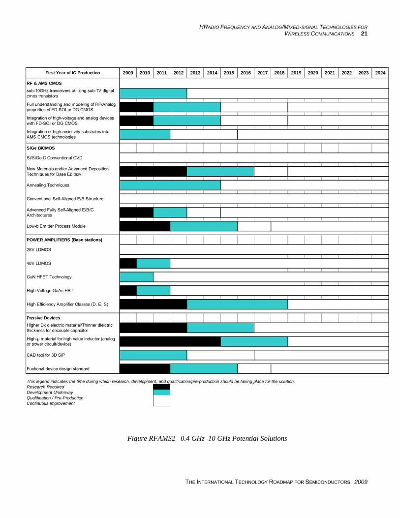


![semiconductors fundamentals.ppt [相容模式] · 2009-02-17 · semiconductors 1. Intrinsic semiconductor is an insulator 2. The conduction property of the SC is determined by the](https://static.documents.pub/doc/80x56/5e79064bb10f26248b3fc636/semiconductors-c-2009-02-17-semiconductors-1-intrinsic-semiconductor.jpg)


