•JCJLT Tennessee Tech 'MJJCJ UNIVERSITY Time-Reversal Based Range Extension Technique for Ultra-wideband (UWB) Sensors and Applications in Tactical Communications and Networking Technical Report (Quarterly) to US Office of Naval Research 875 North Randolph Street Arlington, VA 22203-1995 for Grant # N00014-07-1-0529 Prepared by Robert C. Qiu (Principal Investigator) together with (Contributing Researchers at Wireless Networking Systems Lab) Nan (Terry) Guo Yu Song Peng (Peter) Zhang Zhen (Edward) Hu April 16, 2009 Department of Electrical and Computer Engineering Center for Manufacturing Research Tennessee Technological University Cookeville, TN 38505 20090702327
Transcript
•JCJLT Tennessee Tech 'MJJCJ UNIVERSITY
Time-Reversal Based Range Extension Technique for Ultra-wideband (UWB) Sensors and Applications in Tactical
Communications and Networking
Technical Report (Quarterly)
to
US Office of Naval Research
875 North Randolph Street
Arlington, VA 22203-1995
for
Grant # N00014-07-1-0529
Prepared by
Robert C. Qiu
(Principal Investigator)
together with
(Contributing Researchers at Wireless Networking Systems Lab)
Nan (Terry) Guo Yu Song
Peng (Peter) Zhang Zhen (Edward) Hu
April 16, 2009
Department of Electrical and Computer Engineering
Center for Manufacturing Research
Tennessee Technological University
Cookeville, TN 38505
20090702327
REPORT DOCUMENTATION PAGE Form Approved OMB No. 0704-0188
The public reporting burden for this collection of information is estimated to average 1 hour per response, including the time for reviewing instructions, searching existing data sources, gathering and maintaining the data needed, and completing and reviewing the collection of information. Send comments regarding this burden estimate or any other aspect of this collection of information, including suggestions for reducing the burden, to Department of Defense, Washington Headquarters Services, Directorate for Information Operations and Reports (0704-0188), 1215 Jefferson Davis Highway, Suite 1204, Arlington, VA 22202-4302. Respondents should be aware that notwithstanding any other provision of law, no person shall be subject to any penalty for failing to comply with a collection of information if it does not display a currently valid OMB control number. PLEASE DO NOT RETURN YOUR FORM TO THE ABOVE ADDRESS.
The focus of this report is on major improvement and system test. Receiver sensitivity has been significantly improved and about 3 dB time reversal precoding gain has been observed based on system trial in indoor non-line-ofsight scenario. Theoretical study shows that additional gain can be achieved by using optimum waveform design. Listed below are major achievements during the quarter: • multiple integration window sizes; • comprehensive system test; • improved receiver sensitivity to -81 dBm; • 3 to 4 dB time reversal precoding gain in indoor non-line-of-sight scenario. We will continue to improve the system and conduct more measurements, while seeking some technology transfer
15. SUBJECT TERMS
UWB, testbed, time reversal, range extension, sensors, multi-GHz wideband, cognitive radio
16. SECURITY CLASSIFICATION OF:
REPORT
u
b. ABSTRACT
u
c. THIS PAGE
u
17. LIMITATION OF ABSTRACT
uu
18. NUMBER OF PAGES
24
19a. NAME OF RESPONSIBLE PERSON
Francis Otuonye 19b. TELEPHONE NUMBER (Include area code)
931-372-3374 Standard Form 298 (Rev. 8/98) Prescribed by ANSI Std. Z39.18
I- S o . PC *=
8^ M CD
Q «
< S
Z g O c
O
o I OC ' o s a. ^
" c
a>2 c o - <1) 01 A • o.Q £ £ w -O o « E o y D
•D £ c
c a) o
Hi a> R CO £ S!s
5 s"l a, c > •c £ >• o>0
» E E C •
£25
5 c 3 *- own
2 O) o <0 C "£
ill 5= 3
TJ .c JD
— *- jQ - o _ CO CD —
2 a. •
!Z 2
CD 3
: s 1 . a> —
11 j. -J o
.i £
OC UJ OC n in
El §
h- H O
2 °
HI S 9l » §>5
c o> a li £ C -D O d .2 « S c 2 Q •S . o> g S :•= ssr s:
s|? o o z cc F. LU CC
,« ^ °> LJ - s - "-
P S « uj P
E c £ s g s
-of1 ° " S O c ~ - 01 B
SE?
? c 2 3 C « •Q .9 "g O) O o
5T « ^ - •£ in
:= OJO •? = o
o O S > O
O
OQ Z i < l- "*
O i—I * s s ISO o Z
f-
Q 1
II vC
11
^ «5 8 <* >
.a OO
51 * Q 1 -
u oo
5 z
6 £ '> u
2 § - U
(- Q >? Z in il
1 S a 2 S LU = < o cc 5 H i- £ it « o o Slt 9 > t z
III CC (/) z
1 < o O CC o O O H
£2 2? S -I •D
i z _ CQ — O CC SI- „ IU
< CC CO = o S S z 3 1 i D < Z i-
§ t g i d ff * < I« t m °- *2 < u) o Q-
o h- Q CC is a UJ OC
Z 91
1! z O 1- UJ *J ?
<5 LU
u c o z
z 5 o q 1- o <
a s! a. <
LU •c o
Q Q S? s H O s SF s E LU >- ^
Kis CO IN O
UJ (A
°- p UJ u m <
51 5u • i§ it • O cc -_ LU Z Q o z F = cc o to
pi < 5
5^:
51
S 5
< 5 < <
OC
1- o Z o
< CO CL 3 \- <T>
s U. o O <> UJ CO > 3 < u a o
Z
< CO a a cc o 01 >
10
u- n CO cc
1 c: 0) •o
cc O a. M £ < cc a H Z n CJ •*- o CO 01
w •n
cc o> n u i- o
°- 0) rat c o r tt
o £
P ai »- > *^
E .2 0) *- o c _ 0>
< z
c -a
CA
o CO CD o
to
O > LU LX 0-
Z _(b
H 5
1 o s I- 5 S < 5i U.
° < V 1 2 g1
2 o S .' O
o o CM
c\ 00 00
o LL
Q Q
Acknowledgment
This work has been improved by discussions with S. K. Das (ONR), B. M. Sadler (ARL), R. Ulman (ARO), and L. Lunardi (formerly with NSF). K. Currie (CMR, TTU) has provided a lot of support for this project. S. Parke (ECE, TTU) has supported our research in different ways. We also want to thank P. K. Rajan for helpful discussions.
ONR Technical Report 3
Executive Summary
The focus of this report is on major improvement and system test. Receiver sensitivity has been significantly im- proved and about 3 dB time reversal precoding gain has been observed based on system trial in indoor non-line-of- sight scenario. Theoretical study shows that additional gain can be achieved by using optimum waveform design. Listed below are major achievements during the quarter:
• multiple integration window sizes;
• comprehensive system test;
• improved receiver sensitivity to -81 dBm;
• 3 to 4 dB time reversal precoding gain in indoor non-line-of-sight scenario.
We will continue to improve the system and conduct more measurements, while seeking some technology transfer opportunities.
Contents
I Testbed Development 1
1 Major Improvements 3
1.1 Synchronization Improvements 4
1.1.1 Synchronization Review 4
1.1.2 Frame Structure 5
1.1.3 Dense Pulses 5
1.1.4 Start Pattern Averaging 7
1.1.5 Other modifications 7
1.2 Threshold Adjustment 7
2 FPGA Implementation 9
2.1 FPGA Timing Closure Issues 10
2.2 Major FPGA Implementation Reports 11
3 System Test 13
3.1 DAC Interpolating Filter Measurement 13
3.2 Performance Measurement 16
4 Current and Near-Future Work 19
4.1 Synchronization Optimization 19
4.2 Newer DAC and ADC 19
5
6 CONTENTS
4.3 Non-coherent Threshold-less Detection 20
4.4 2-by-l MISO 20
4.5 Direct-Conversion Receiver 20
4.6 Real-Time Error Rate Measurement 21
4.7 Implementation of a Compressed Sensing Based Communication System 22
II Theoretical Work 23
5 Wideband Waveform Optimization with Energy Detector Receiver in Cognitive Radio 25
5.1 Introduction 26
5.2 System Description and Optimal Waveform 26
5.3 Wideband Waveform Design in Cognitive Radio 29
5.4 Numerical Results 34
5.5 Discussion 36
Parti
Testbed Development
Chapter 1
Major Improvements
CHAPTER I. MAJOR IMPROVEMENTS
Our major development work in the last quarter is to test and modify the system. The most significant part is the synchronization at the receiver side.
1.1 Synchronization Improvements
For a burst mode radio system, the synchronization has always been a challenge. In order to make the synchro- nization more robust for the test-bed, we have made some improvements, which include modification of the frame structure, average samples for start pattern searching and various thresholds adjustment.
1.1.1 Synchronization Review
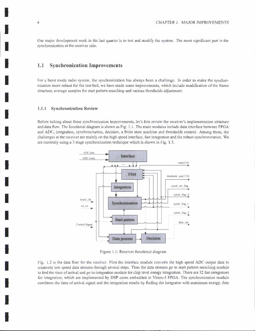
Before talking about these synchronization improvements, let's first review the receiver's implementation structure and data flow. The functional diagram is shown as Fig. 1.1. The main modules include data interface between FPGA and ADC, integration, synchronization, decision, a finite state machine and thresholds control. Among them, the challenges at the receiver are mainly on the high speed interface, fast integration and the robust synchronization. We are currently using a 3 stage synchronization technique which is shown in Fig. 1.3.
Control Signal
Figure 1.1: Receiver functional diagram
Fig. 1.2 is the data flow for the receiver. First the interface module converts the high speed ADC output data to relatively low speed data streams through several steps. Then the data streams go to start pattern searching module to find the time of arrival and go to integration module for chip level energy integration. There are 32 fast integrators for integration, which are implemented by DSP cores embedded in Virtex-5 FPGA. The synchronization module combines the time of arrival signal and the integration results by finding the integrator with maximum energy, then
1.1. SYNCHRONIZATION IMPROVEMENTS
it gets the chip threshold. After that the receiver applies frame level synchronization to find the fine timing and make decisions. The finite state machine and variable thresholds control module coordinate all the processes.
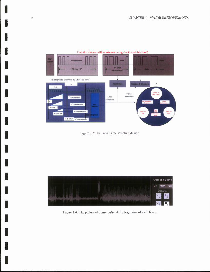
The system is supposed to find the window with maximum energy in every 40 ns, which is the chip period. Fig. 1.3 shows the new frame structure of the system. The first stage is to search the time of arrival; the second stage is to average 128 chips energy to find the chip threshold; the third stage is to synchronize the whole frame. Data demodulation is performed after the three-stage synchronization. Fig. 1.3 also shows the sliding window integration diagram and the state transition diagram.
The modification in the synchronization head does not change the overall frame structure. The following parameters are kept: system's frame length: 4096 chips or 163.84 ^/s; payload efficiency: 94.49%; chip sync accuracy: one sample (1.25 ns); and frame sync accuracy: one chip (40 ns). If the overall clock accuracy is 20 PPM, then the maximum time drift is 163.84 x 10"6 = 3.276 /us.
1.1.3 Dense Pulses
However, even though we averaged the start pattern searching, we observed that the synchronization error still mainly comes from the first stage. In this stage, the threshold is very sensitive to noise level and DC offset of ADC sampling, especially for longer distance transmission. So we try to send 5 chips long dense pulses at the beginning of each frame to make sure the time of arrival is found each frame since the average value of these chips should be much higher than ordinary ones. Fig. 1.4 shows the real picture of dense pulses at the beginning of each frame.
CHAPTER 1. MAJOR IMPROVEMENTS
Find the window with maximum energy in 40 ns (Chip level)
Figure 1.3: The new frame structure design
i Cursoi Souice
C h Math Ret Channel
,%»*40Mi »~« itflUliliiiiiillai IB I*JH [ a_
Figure 1.4: The picture of dense pulse at the beginning of each frame
1.2. THRESHOLD ADJUS TMENT
1.1.4 Start Pattern Averaging
For the first synchronization stage, we accumulate the values of 32 consecutive samples and compare it with a threshold to claim whether it is one frame's time of arrival. However, due to the interference and environment's uncertainty, the first stage result should not be so reliable when it just counts on the value only one chip time, because the time frame is too short. So we try to average two chip time samples result to get the averaged value, and compare it with a threshold, Fig. 1.5 shows the diagram of this improvement, where we set a more strict condition to claim the time of arrival result by comparing 5 times(or other number) instead of only one, and is in 5 chips time(or other number), 3 high results are needed to claim the first stage synchronization result. After that, because we send dense pulses at the beginning of each frame and there is a interval between the pulses and the real chips, we delay two chips time before the beginning of second stage.
1.1.5 Other modifications
For the third stage,we also utilized 60 bits M sequence instead of 60 bits OOC code for frame synchronization. This is mainly because the randomness of M sequence is much better than OOC code.
For time reversal system and non time reversal system, the received pulses are very different at the width, typically 6 ns for time reversal and 15 ns for non time reversal. So in the energy integration module, the window size for integration should be different for different signal scenarios. This parameter is to be adjusted in integration module, as described in the last quarter report.
1.2 Threshold Adjustment
For energy detection based receiver, it is well known that the performance depends significantly on the choice of threshold level. A good threshold can be determined by using some channel quality indicator and feedback information provided by the digital processor (back-end) at the receiver. There is an optimum threshold for lowest error rate. To deal with ISI situation, it is proposed to set a threshold based on two worst signal cases.
One phenomenon discovered is that a mono-bit ADC along with proper thresholding can be applied for quantizing the pre-filters coefficients, and the resulting signal still gets focused. It enables the development of a unique time reversal system with much lower complexity. Major points include: (1) optimization of the threshold for quantiza- tion; (2) development of an adaptive threshold method; (3) impact of tap spacing and length of the pre-filter. In our case, there are 4 variable thresholds at the receiver side with each corresponds to different stages of synchronization and detection. They are the threshold for start pattern searching, the threshold for ADC bias shift, the code distance for frame level synchronization and the threshold of chip threshold determine at the second synchronization stage. All these values are adjusted by the pushbuttons on the receiver Virtex-5 board and the led lights can show any threshold's adjustment level.
DC offset causes performance degradation in signal processing systems especially for high-speed applications. For our ADC board in the receiver side, the DC shift makes the true quantization value hard to determine, thus makes the threshold vulnerable, especially for the energy detection based receiver with OOK modulation. DC offset can be reduced in real-time by subtracting the mean amplitude from each sample, or by calibrating the ADC board.
CHAPTER I. MAJOR IMPROVEMENTS
0 Data input
32 samples 32 samples
Accu nulate Accur nulate Accurr ulate
Result 1
32 samples
Result 2 Result 3
Start pattern claim
The old start pattern searching
^ 40 ns ^
i ^ 32 samples Data input
32 samples
Accu nulate Accur nulate Accun ulate
Result 1
32 samples
Result 2 Result 3
I *<+>. 1 *(+)* 1 >(+)* 1
Average 1 Average 2 Average 3
Decision 3 Decision N
Start pattern claim
The new start pattern searching
Figure 1.5: Start pattern searching improvement
Chapter 2
FPGA Implementation
10 CHAPTER 2. FPGA IMPLEMENTATION
2.1 FPGA Timing Closure Issues
For FPGA implementation, meeting timing requirements in speed-critical designs has been always a challenge, and this is often an iterative process ensuring that each and every path in the design meets the required timing. Meeting timing closure is easy and automatic for relatively slow or small designs. However, most designs do not fall into that happy category and as each critical path is adjusted in order to meet timing, new ones are uncovered or created anew. In the case of FPGAs implemented at the 65nm technology node, for example, wire delays can account for 80-to-90% of each path's delay.
An important technique for achieving successful timing closure on an aggressive design is to carefully review the most critical timing constraints. In our case, there are two critical paths at the transmitter: one is from the data loading module to the waveform generator module where huge parallel data steams exist, another critical path is in the parallel to serial conversion module requiring high clock rate. At the receiver side, the most critical path is from the integration module to the synchronization module which performs fast timing acquisition in parallel manner. Achieving clock-to-clock (global) timing for all internal signals in a synchronous design may be easy, but this simple approach will usually overconstrain the design and eventually lead to a failure. Therefore, we have applied different constraints to different paths depending on their timing requirements.
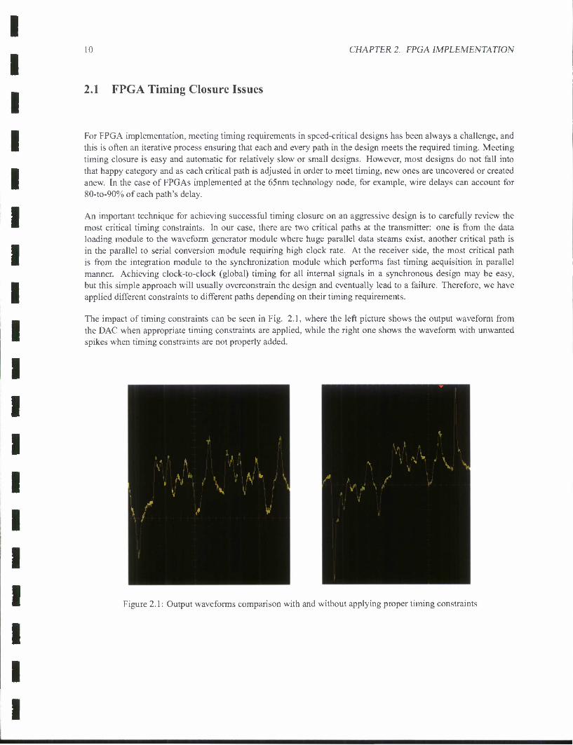
The impact of timing constraints can be seen in Fig. 2.1, where the left picture shows the output waveform from the DAC when appropriate timing constraints are applied, while the right one shows the waveform with unwanted spikes when timing constraints are not properly added.
U , A
• jt, ! *
Figure 2.1: Output waveforms comparison with and without applying proper timing constraints
2.2. MAJOR FPGA IMPLEMENTATION REPORTS 11
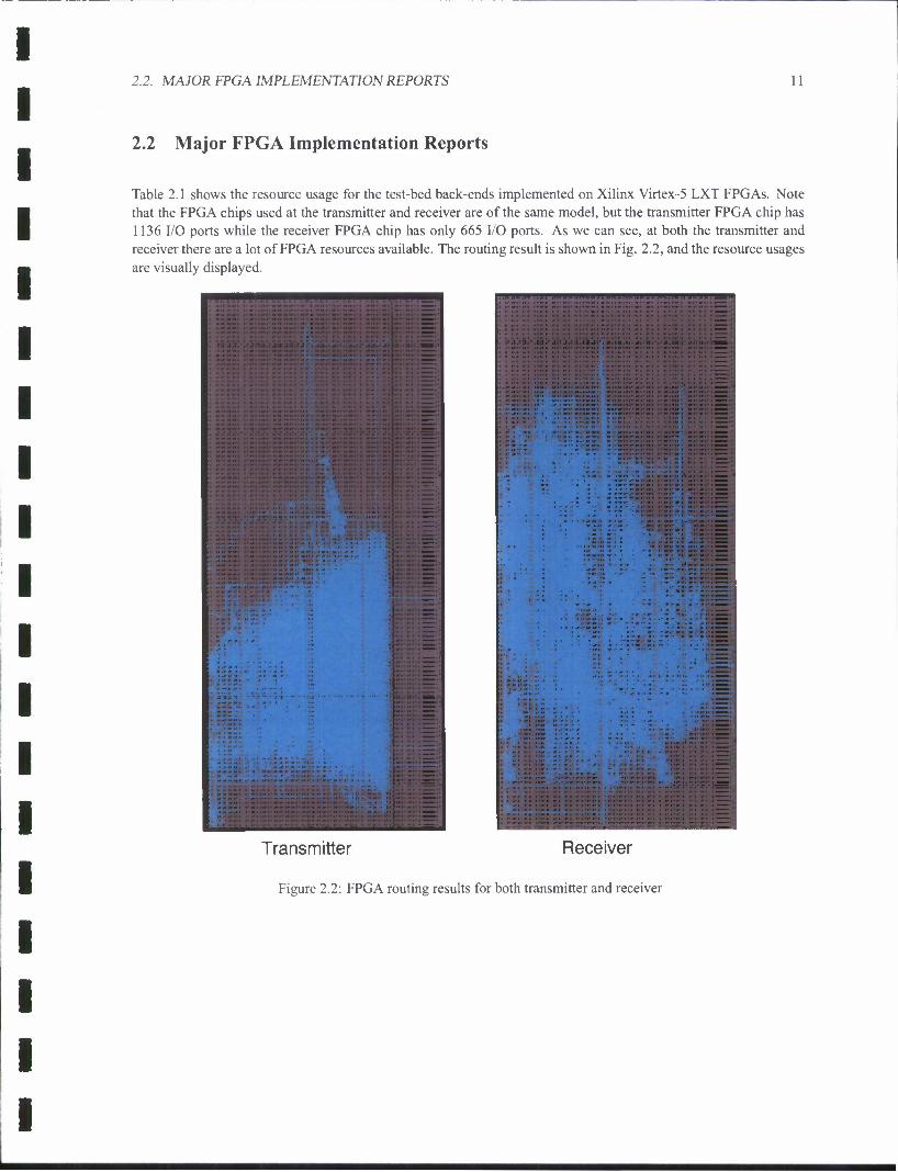
2.2 Major FPGA Implementation Reports
Table 2.1 shows the resource usage for the test-bed back-ends implemented on Xilinx Virtex-5 LXT FPGAs. Note that the FPGA chips used at the transmitter and receiver are of the same model, but the transmitter FPGA chip has 1136 I/O ports while the receiver FPGA chip has only 665 I/O ports. As we can see, at both the transmitter and receiver there are a lot of FPGA resources available. The routing result is shown in Fig. 2.2, and the resource usages are visually displayed.
••••••••••MMI I 1 -J...J-JMMH l.ll .1J...I.I.I.I-...
Figure 2.2: FPGA routing results for both transmitter and receiver
12 CHAPTER 2. FPGA IMPLEMENTATION
Table 2.1: FPGA Implementation statistics at transmitter and receiver Transmitter Transmitter Receiver Receiver
Resources Amount used Percent used Amount used Percent used Number of Slice Registers 5314 18% 4184 14% Number of Slice LUTs 5019 13% 3088 10% Number of occupied Slices 1719 24% 1713 23% Number of bonded IOBs 40 8% 90 25% Number of BlockRAM/FIFO 2 3% 1 1% Number of BUFG/BUFGCTRLs 7 21% 10 31% Number of DSP48Es NA NA 32 66% Total equivalent gate count 275,214 NA 195438 NA
Chapter 3
System Test
3.1 DAC Interpolating Filter Measurement
The equivalent baseband filter in the transmitter-receiver chain has to be taken into account in order to have optimum waveform at the receiver detector. This filter is generally not flat over the frequency band of interest, especially for wide bandwidth case. Estimating and controlling the equivalent baseband filter is not easy. As shown in Fig. 3.1, the overall filter effect is contributed from three sources: the DAC's interpolating filter p(t) and RF front-ends including antennas at both sides. By omitting some scalar factor, the equivalent filter in baseband format is
F(t) = F0(t)®Fl(t)®F2(t), (3.1)
and F0(t) can be expressed using the interpolating filter p(t)
F0(t)=p(t)+j-p(t). (3.2)
According to our measurement, the shape of the equivalent filter is dominated by the interpolating filter p{t). Based on the ADC used in the testbed, p(t) has been accurately measured and Fo(t) = p(t) + j • p(t) has been used as an estimate of F(t).
To measure the filter, a full scale (14-bit) 1-ns wide digital pulse directly generated in the FPGA chip is used as a trigger source, resulting in a analog pulse at the DAC's output. This pulse, as shown in Fig. 3.2, is actually the interpolating pulse shape (filter) corresponding to sampling rate of 1 Gs/s. The pulse width is over 1 ns and there is a tail behind the pulse, implying imperfect circuit coupling. The spectrum of the interpolating filter is depicted in Fig. 3.3.
13
14 CHAPTER 3. SYSTEM TEST
FPGA DA
Fo(t)
Interpolating filter p(t)
l/Q Modulator
Re{Fi(t)exp(j2pi.fc)} V
Local oscillator
Transmitter
r Re{F2(t)exp(j2pi.fc)} V"7 I
FPGA A/D Amp LPF Detector LNA BPF
i
Receiver
Figure 3.1: Equivalent filter in transmitter-receiver chain (not including the propagation channel), contributed from three sources.
» 0.15r
.5
I 0.1 •
I
10 20 30 40 Time {ns)
Figure 3.2: Measured interpolating pulse shape.
3.1. DAC INTERPOLATING FILTER MEASUREMENT 15
Frequency (GHz)
Figure 3.3: The spectrum of the interpolating filter.
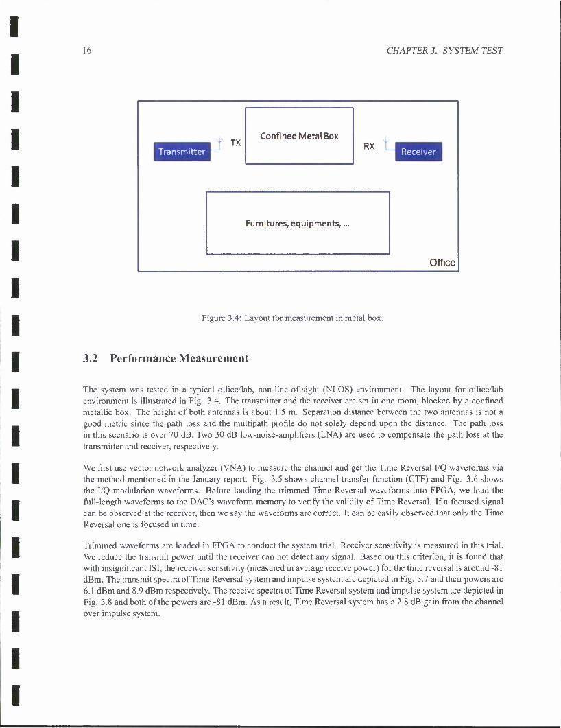
16 CHAPTER 3. SYSTEM TEST
TX Transmitter
Confined Metal Box RX
Receiver
Furnitures, equipments, ...
Office
Figure 3.4: Layout for measurement in metal box.
3.2 Performance Measurement
The system was tested in a typical office/lab, non-line-of-sight (NLOS) environment. The layout for office/lab environment is illustrated in Fig. 3.4. The transmitter and the receiver are set in one room, blocked by a confined metallic box. The height of both antennas is about 1.5 m. Separation distance between the two antennas is not a good metric since the path loss and the multipath profile do not solely depend upon the distance. The path loss in this scenario is over 70 dB. Two 30 dB low-noise-amplifiers (LNA) are used to compensate the path loss at the transmitter and receiver, respectively.
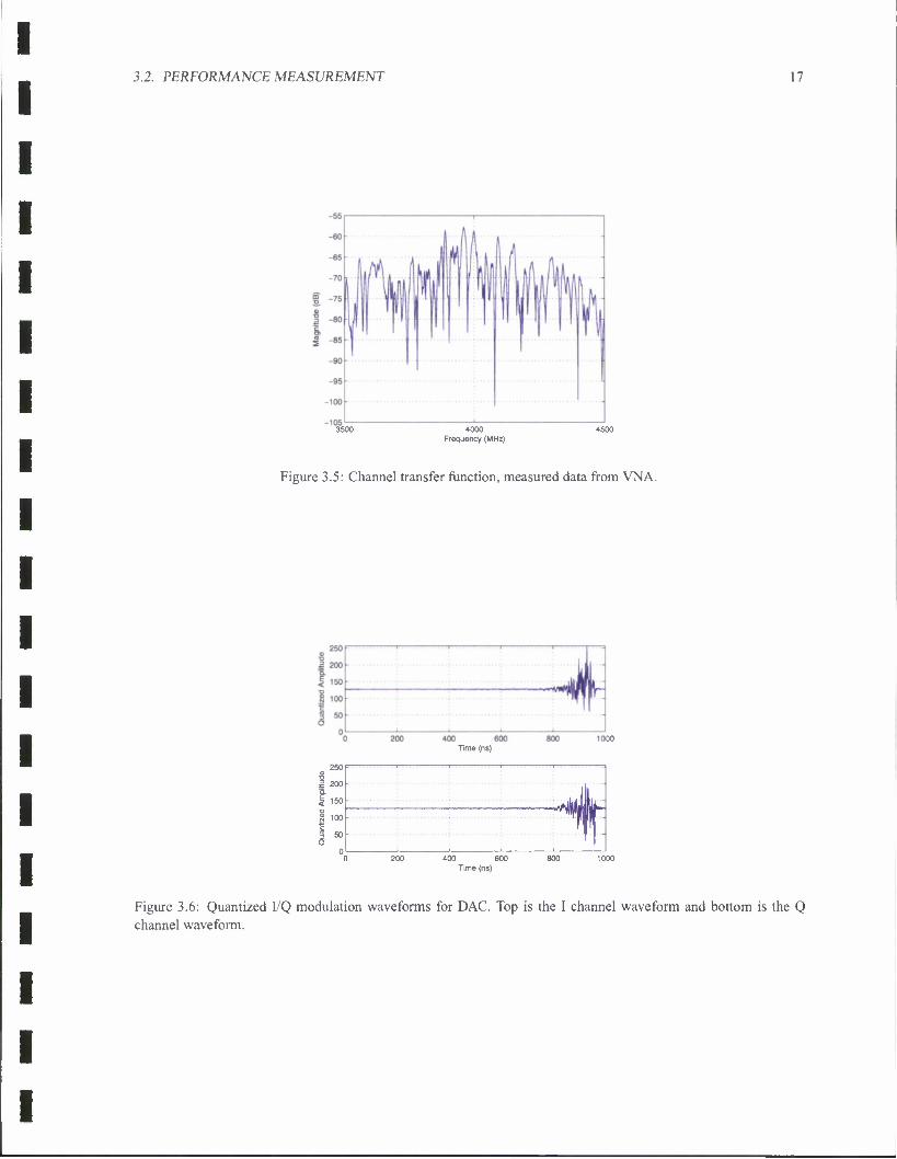
We first use vector network analyzer (VNA) to measure the channel and get the Time Reversal I/Q waveforms via the method mentioned in the January report. Fig. 3.5 shows channel transfer function (CTF) and Fig. 3.6 shows the I/Q modulation waveforms. Before loading the trimmed Time Reversal waveforms into FPGA, we load the full-length waveforms to the DAC's waveform memory to verify the validity of Time Reversal. If a focused signal can be observed at the receiver, then we say the waveforms are correct. It can be easily observed that only the Time Reversal one is focused in time.
Trimmed waveforms are loaded in FPGA to conduct the system trial. Receiver sensitivity is measured in this trial. We reduce the transmit power until the receiver can not detect any signal. Based on this criterion, it is found that with insignificant ISI, the receiver sensitivity (measured in average receive power) for the time reversal is around -81 dBm. The transmit spectra of Time Reversal system and impulse system are depicted in Fig. 3.7 and their powers are 6.1 dBm and 8.9 dBm respectively. The receive spectra of Time Reversal system and impulse system are depicted in Fig. 3.8 and both of the powers are -81 dBm. As a result, Time Reversal system has a 2.8 dB gain from the channel over impulse system.
3.2. PERFORMANCE MEASUREMENT 17
4000 Frequency (MHz)
Figure 3.5: Channel transfer function, measured data from VNA.
400 600 Time (ns)
200
150
100 •
50 • ; 4i 400 600
Time (ns)
Figure 3.6: Quantized I/Q modulation waveforms for DAC. Top is the I channel waveform and bottom is the Q channel waveform.
18 CHAPTER 3. SYSTEM TEST
4000 Frequency {MHz)
Figure 3.7: Transmit spectra for Time Reversal system and impulse radio system.
£ -
4000 Frequency {MHz)
Figure 3.8: Receive spectra for Time Reversal system and impulse radio system.
Chapter 4
Current and Near-Future Work
Although a gain contributed by time reversal precoding has been achieved, we believe there are still some room to improve the hardware implementation and the performance. Moreover, we have started to design a new test-bed with compressive sensing capability.
4.1 Synchronization Optimization
The proposed 3-stage synchronization scheme follows proper design philosophy for burst mode communication. We have found that the synchronization performance varies depending on the system configuration. There are a number of parameters that may need to be optimized. However, globally optimizing the overall synchronization performance is too challenging. A practical optimization strategy is to combine pure analysis, measurement and simulation. A detailed methodology needs to be investigated before starting the optimization process.
4.2 Newer DAC and ADC
The DAC (MAX 108) used in the receiver is not ideal in terms of sampling rate and connection. We are planning to replace it with some newer product to reach a sampling rate of 2 Gs/s or above. Current the sampling rate is only 800 Ms/s, which might cause performance degradation since the time reversal pulse width at the detector's output is only 6 ns at the half height. If the sampling rate increases to 2 Gs/s, 12 samples can be effectively captured for each received pulse. The current connection between the ADC and the FPGA board is loose and the individual path lengths for different bits of a sample are not accurately aligned mainly due to physical PCB routing limitation in the cable-connector adapting PCB.
A high speed ribbon cable/bus has been successfully used to connect the DAC and the FPGA board in the transmitter. However, It is doubtable for this type of cables to meet our higher sampling rate requirement. One solution to the bottleneck caused by connection is to use a signal processing package with an ADC (or a DAC) and an FPGA chip integrated on a single board. We are searching such type of boards and evaluating their performance to price ratios.
19
20 CHAPTER 4. CURRENT AND NEAR-FUTURE WORK
4.3 Non-coherent Threshold-less Detection
OOK modulation has been adopted in the system mainly for its simplicity for non-coherent detection. The number one bothering problem in the system with OOK modulation and non-coherent detection is the sensitivity to the decision threshold. An optimum threshold depends on the SNR at the receiver, and it requires sophisticated signal processing to achieve the optimum, which prevents the performance from being the optimum practically.
Per above discussion, non-coherent threshold-less detection is extremely desired. One solution is a combination of PPM modulation and non-coherent detection. Shown in Fig.4.1 is a conceptual receiver block diagram for PPM modulation with non-coherent detection.
^y^ Integration &
Dump
1 >0 < 0
r(t) ( )A2
S1-S0
Figure 4.1: Conceptual receiver block diagram for PPM modulation with non-coherent detection
4.4 2-by-l MISO
A 3-dB array gain can be anticipated if the number of transmitter branches increases from one to two. For the passband signaling approach, the carriers in the two branches must be strictly aligned, which requires identical DACs, modulators and power amplifiers in the both branches. The two branches can share a common local oscillator (LO). We are currently searching devices for this matter.
4.5 Direct-Conversion Receiver
To explore more communication techniques, especially those implemented at receiver side, a coherent receiver will provide more potential than a non-coherent receiver. Among all coherent receiver architectures is a direct- conversion receiver which is popular nowadays. This type of receiver is also called homodyne, synchrodyne or zero-IF receiver. An attractive feature of a direct-conversion receiver is that it requires less analog processing but more digital processing. This feature favors our design philosophy in terms of flexibility, thus it has been considered as our new receiver. In UWB band, a modulation-demodulation scheme to test on this receiver might be transmitted reference or its variants.
4.6. REAL-TIME ERROR RATE MEASUREMENT 21
4.6 Real-Time Error Rate Measurement
So far we have tested frame loss rate (due to synchronization failure) and bit error rate in a non-real-time way. A real-time error meter will be extremely desired since it can serve as an indicator in a system trial and make the measurement more efficient and effective. A stand-alone real-time error meter mainly consists of a data acquisition section as well as a data processing section, and it can be virtually used in different situations. A difficult part of a stand-alone error meter is to synchronize the meter with the incoming data stream.
22 CHAPTER 4. CURRENT AND NEAR-FUTURE WORK
4.7 Implementation of a Compressed Sensing Based Communication System
We propose an implementable Compressed Sensing (CS) based communication system, as illustrated in Fig. 4.2. A 1 Ghz UWB signal is transmitted in the 10 GHz carrier and captured by a 25 Msps A/D. This system utilizes the concept in the October 2008's report but with smaller bandwidth. This is due to the limitation of available RF hardware. The baseband signal must be modulated to carrier frequency because no antennas can transmit signal with frequency starting from DC. Sparse pulse position modulation (PPM) data is digitally filtered by a high rate PN filter in FPGA. For a Xilinx Virtex 5 FPGA, the rate of output signal can be up to 3.2 Gsps thanks to the advanced RocketIO technology. The circuity in FPGA acts as a virtual interpolating filter, transforming digital signal into analog waveform. Alternatively, we can build a PN sequence generator with rate up to even 80 Gsps by standard high rate shift register. However, this is not implementable due to the limitation of the state-of-art RF technology. To the best knowledge of the author, the largest bandwidth supported by a modulator is 1 GHz, provided by MITEQs SDM1015LI3CDQ with 10 GHz - 15 GHz RF output. As a result, the output signal bandwidth from FPGA should not exceed 1 GHz. Power amplifier (PA) is used before transmitting the UWB signal over the air. The structure of the receiver is very simple. There is no down-conversion. A 25 Msps A/D samples the data directly after a low noise amplifier (LNA) and passband filter. FPGA is used to acquire the A/D data and process with recovery algorithms such as OMP, StOMP, etc..
The following is a list of key hardware found in the market in Fig. 4.2:
• FPGA: Xilinx Virtex 5 LX330T with 3.25 Gsps RocketIO
• Modulator: MITEQ SDM1015LI3CDQ with 1 GHz modulation bandwidth, 10 GHz - 15 Ghz RF output frequency
• Local Oscillator: MITEQ LPLM15000 with 8 GHz - 15 GHz output frequency
• PA: MITEQ AMF-6B-08001800-60-34P with 8 GHz - 18 GHz frequency range, 37 dB gain
• LNA: MITEQ AMFW-5S-10001500-250 with 10 GHz - 15 GHz frequency range, 30 dB gain
UWB Siflnal wtthl -GHi
Figure 4.2: Architecture of a proposed compressed sensing based communication system.
Part II
Theoretical Work
23
Chapter 5
Wideband Waveform Optimization with Energy Detector Receiver in Cognitive Radio
25
26CHAPTER 5. WIDEBAND WAVEFORM OPTIMIZATION WITH ENERGY DETECTOR RECEIVER IN COGNITIV
5.1 Introduction
Waveform design or optimization is a key research issue in the current wireless communication system. Waveform should be designed according to the different requirements and objectives of system performance. For example, the waveform should be designed to carry more information to the receiver in terms of capacity. For navigation and geolocation, the ultra short waveform should be used to increase the resolution. If the energy detector is employed at the receiver, the waveform should be optimized such that the energy of the signal within integration window at the receiver should be maximized. In the context of cognitive radio, waveform design or optimization gives us more flexibility to design a radio which can coexist with other cognitive radios and primary radios. From cognitive radio's point of view, spectral mask constraint at the transmitter and the influence of Arbitrary Notch Filter at the receiver should be seriously considered for waveform design or optimization, except the consideration of the traditional com- munication objectives. Spectral mask constraint is imposed on the transmitted waveform such that cognitive radio has no interference to primary radio. While Arbitrary Notch Filter at the receiver is used to cancel the interference from primary radio to cognitive radio. Though Arbitrary Notch Filter is at the receiver, the influence of Arbitrary Notch Filter should be incorporated into waveform design at the transmitter. How to implement Arbitrary Notch Filter is out of scope of this chapter.
The optimization problem is formulated as Quadratically Constrained Quadratic Program (QCQP), which is known as an NP-hard problem. However, after relaxation, QCQP can be solved by using Semidefinite Program (SDP) plus a randomized algorithm. In addition to SDP, a computationally-efficient iterative method is proposed to give the optimal solution for a special situation where the integrator only captures one sample after ADC as the decision statistic.
5.2 System Description and Optimal Waveform
The system architecture is shown in Figure 5.1. We limit our discussion to a single-user scenario, and consider the transmitted signal with OOK modulation given by
s(t)= Y, djP(t-jTb) (5.1) j=—oo
where Tb is the symbol duration, p(t) is the transmitted symbol waveform defined over [0, Tp] and dj S {0,1} is the j-th transmitted bit. Without loss of generality, assume the minimal propagation delay is equal to zero. The energy of p(t) is Ep,
I Jo
pz (t) dt = Ep (5.2)
and the frequency domain representation of p(t) is p/(/). Thus,
\Pf (f)\2 df = Ep (5.3)
/
The received noise-polluted signal at the output of low noise amplifier (LNA) is
r(t) = h(t)®s{t)+n(t) (5.4)
= Y, djX(t-jTb)+n{t) (5.5) J = -CC
5.2. SYSTEM DESCRIPTION AND OPTIMAL WAVEFORM 27
Tx FPGA
Baseline Trans milter
Arbitrary Waveform Generatoi
DA
RxFPGA
A A/D kLEncrgy, Detector
Power Amplifier
h(t)
Arbitrary Notch Filter
A/
\f
Figure 5.1: System architecture.
where h(t) ,t G [0, Th] is the multipath impulse response that takes into account the effect of channel impulse response, the RF front-ends in the transceivers such as Power Amplifier, LNA and Arbitrary Notch Filter as well as antennas. h(t) is available at the transmitter [1] [2] and the energy of h(t) is Eh,
P h2 (t) dt = Eh
and the frequency domain representation of h(t) is hf(f). Thus,
\hf(f)\2df = Eh I
•I
(5.6)
(5.7)
"<g>" denotes convolution operation. n(t) is a low-pass additive zero-mean Gaussian noise with one-sided bandwidth W and one-sided power spectral density NQ. x(t) is the received noiseless symbol-"!" waveform defined as
x{t) = h(t)®p{t) (5.8)
def We further assume that Tb>Th + Tp = Tx, i.e. no existence of ISI.
An energy detector performs square operation to r(t). Then the integrator does the integration over a given integra- tion window T/. Corresponding to the time index k, the k-th decision statistic at the output of the integrator is given by
rkTb+TIa+Ti zk= / r2{t)dt
JkTb+T,0
rkTb+T,o+T, = / {dkx{t-kTb)+n{t))2dt
JkTb+T,a
(5.9)
(5.10)
where Tj0 is the starting time of integration for each symbol and 0 < Tj0 < TJQ + T[ <TX < Tb.
An approximately equivalent SNR for the energy detector receiver, which provides the same detection performance when applied to a coherent receiver, is given as [3]
SNR^, z($0°
+Tl*2(t)dt)'
2.3T!\VN2 + NQ £0+T; x2 {t) dt
(5.11)
2&CHAPTER5. WIDEBAND WAVEFORM OPTIMIZATION WITH ENERGY DETECTOR RECEIVER IN COGNITIV
For best performance, the equivalent SNR SNReq should be maximized. Define,
rTjo+Tj Ei = / x2{t)dt (5.12)
JTio
For given T/, No and W, SNReq is the increasing function of £/. So the maximization of SNReq in Equation 5.11 is equivalent to the maximization of Ei in Equation 5.12.
So the optimization problem to get the optimal p(t) is shown below,
fTiu
>J"> (5.13) max J^+T'x2(t)dt
s.t.JQTpp2(t)dt = Ep
In order to solve the optimization problem 5.13, a numerical approach is employed in this document. In other words, p(t), h(t) and x(t) are uniformly sampled (assumed at Nyquist rate), and the optimization problem 5.13 will be converted to its corresponding discrete-time form. Assume the sampling period is Ts. Tp/Ts = Np and Np is assumed to be even, Th/T3 = Nh and Tx/Ts = Nx. So Nx = Np + Nh.
p(t), h(t) and x(t) are represented by pi, i = 0,1,..., Np, hi,i = 0,1,..., Nh and x%, i = 0,1,..., Nx respec- tively [3].
Define, P= [poPi •• PNP}T (5.14)
and x = [x0 xi ••• xNx]T (5.15)
Construct channel matrix H(NX+I)X(NP+I)'
m«-{V0 *."'** <516)
where (•)l denotes the entry in the i-th row and j'-th column of the matrix or vector. Meanwhile, for vector, taking p as an example, (p)^ j is equivalent to p»-i.
The matrix expression of Equation 5.8 is, x = Hp (5.17)
and the constraint in the optimization problem 5.13 can be expressed as,
\\p\\22Ts = Ep (5.18)
where "||»||2" denotes the norm-2 of the vector. In order to make the whole document consistent, we further assume,
I|P||2 = 1 (5-19)
Let Ti/Ts = Ni and T/o/T, = JV/o. The entries in x within integration window constitute x/ as,
x/ = lxNI0 xNI0+l ••• XNI0+N,}T (5.20)
5.3. WIDEBAND WAVEFORM DESIGN IN COGNITIVE RADIO 29
and Ei in Equation 5.12 can be equivalently shown as,
EI = \\xI\\lTs (5.21)
Simply dropping Ts in Ej will not affect the optimization objective, so Ej is redefined as,
Ei = ||x,||£ (5.22)
Similar to Equation 5.17, x/ can be obtained by,
x, = H/P (5.23)
where (H/)y = (H)Nio+lJ and i = 1,2,..., AT/ + 1 as well as j = 1,2,..., Np + 1.
The optimization problem 5.13 can be represented by its discrete-time form as,
max £7
Si.||P||2 = l (5.24)
The optimal solution p* for the optimization problem 5.24 is the dominant eigen-vector in the following eigen- function [3],
Hf H/P = Ap (5.25)
Furthermore, E*{ will be obtained by Equation 5.22 and Equation 5.23.
5.3 Wideband Waveform Design in Cognitive Radio
For cognitive radio, there is a spectral mask constraint for the transmitted waveform. Based on the previous discus- sion, p is assumed to be the transmitted waveform and F is the Fourier transform matrix, thus the frequency domain representation of p is,
P/ = Fp (5.26)
where p/ is a complex value vector. If the i-th row of F is f», then each complex value in p^ can be represented by,
(p/).1 = fip,i = l,2,...,^ + l (5.27)
Thus the modulus of the complex value is |»|.
Define,
F, = f//fi,z = l,2,...,^£ + l (5.28)
Given the spectral mask constraint in terms of power spectral density c
2
C\ C2 • • • c JV. 2 T1
T , so
(P/)u |f*P|2 (5.29)
= PTfff,P (5.30)
= PTF,P (5.31)
< a,i = l,2,...,-£ + l (5.32)
30CHAPTER 5. WIDEBAND WAVEFORM OPTIMIZATION WITH ENERGY DETECTOR RECEIVER IN COGNITIV
So the optimization problem with spectral mask constraint can be expressed as,
max £/
l|p|la<l PTFlP < ci (5 33)
Define, H0 = HfH7 (5.34)
Equation 5.22, Equation 5.23 and Equation 5.34 are put into the optimization problem 5.33, and then this optimiza- tion problem will be formulated as,
maxpTH0p
PTP<1 PTFip < ci ,5 35x
s.t.
PTF^+1P < <^+1
In the optimization problem 5.35, both the objective function and the constraints are quadratic functions, so this kind of optimization problem is a QCQP. The general QCQP is a NP-hard problem. A semidefinite relaxation method is used in this document to give the suboptimal solution to the optimization problem 5.35.
Define, P = PP
r (5.36)
So P should be the symmetric positive semidefinite matrix, i.e. P >-= 0 and rank of P should be equal to 1.
Rank constraint is nonconvex constraint, so after dropping it, QCQP is relaxed to SDP,
max trace (H0P) trace (P) < 1
trace (FiP) < cx
s.t. (5.40)
trace (F/v^ P) < CNJ \ 2 "*" / 2 ̂+i
The optimal solution P* of the optimization problem 5.40 can be obtained by using CVX tool [4] and the value of the objective function gives the upper bound of the optimal value in the optimization problem 5.35. If the rank of
5.3. WIDEBAND WAVEFORM DESIGN IN COGNITIVE RADIO 31
P* is equal to 1, then the dominant eigen-vector of P* will be the optimal solution p* for the optimization problem 5.35. But if the rank of P* is not equal to 1, the dominant eigen-vector of P* can not be treated as the optimal solution for the optimization problem 5.35, because of the violation of bound constraint.
An efficient randomized algorithm is given by [5] [6] to obtain the feasible solution p* from P*.
This algorithm will be repeated a sufficient number of times to get the relatively good feasible p* as the suboptimal solution to the optimization problem 5.35.
When Ti approaches zero, which means the integrator only captures one sample after ADC as the decision statistic, the maximization of Ej will be equivalent to the maximization of x (T/o). An iterative algorithm is proposed here to give the solution to the maximization of x (T/o), which will be more computationally efficient than the previous semidefinite relaxation method. For the simplicity of the following presentation, T/o is assumed to be zero.
From the inverse Fourier transform, /oo
Xfifte^df (5.41) -oo
and from Equation 5.8, Xf(f)=hf(f)pf(f) (5.42)
where xj (/) is the the frequency domain representation of x(t) respectively.
So, /oo
xf(f)df (5.43) •OO
/OO
hf(f)Pf(f)df (5.44) •oo
If there is no spectral mask constraint, then according to the Cauchy—Schwarz inequality,
/oo hf(f)Pf(f)df (5.45)
•oo
/ /-OO /-OC
< .// \hf(f)\2df \Pf(f)\
2df (5.46) y J—oo J—oo
= y/Etfp (5.47)
when pf (/) = ah*f (/) for all /, the equality is obtained. In this case, p(t) — ah(-t), which means the optimal waveform is the time reversed multipath impulse response. And,
(5.48)
If there is a spectral mask constraint, then the following optimization problem will become more complicated.
maxx (0)
*-*.n>/(/)|2#<l (5.49) |p/(/)|2<C/(/)
32CHAPTER 5. WIDEBAND WAVEFORM OPTIMIZATION WITH ENERGY DETECTOR RECEIVER IN COGNITIV
where Cf (/) represents the arbitrary spectral mask constraint.
Because pf(f) is the complex value, the phase and the modulus of p/(/) should be determined.
/oo hf(f)pf(f)df (5.50)
-OO
/OO
\hf (f)\e^Mhf(f)) \pf (/)| e^arg(P/(/))d/ (5 51)
-oo /OO
Ify (/)l \Pf (f)\ eMMhfU))+MPiU)))df (5.52) •OO
where the angular component of the complex value is arg (•).
For the real value signal x{t), */(/)=*}(-/) (5.53)
If h(f) and |p/ (/)| is given, maximization of x (0) is equivalent to setting,
axg (/»(/))+arg (p(/))=0 (5.57)
which means the angular component of pj (/) is the negative angular component of hf (/).
The optimization problem 5.49 can be simplified as,
max/-°°JM/)llM/M s-t.S-oo\Pf(f)\2df<l (5-58)
|p/(/)|2<c/(/),/>0
Because,
IM/)I = IM"/)I (5-59) \Pf(f)\ = \Pf(-f)\ (5-60)
|c/(/)| = |c/(-/)| (5.61)
for all /. Thus uniformly discrete frequency points /o, ..., /M are considered in the optimization problem 5.58. Meanwhile, /o corresponds to the DC component and f\,..., /M correspond to the positive frequency component.
Define vector hf,
IM/i-i)|,i = l v/2>/(/*-i)|,i = 2,...,^ + l (h/)u = {
5.3. WIDEBAND WAVEFORM DESIGN IN COGNITIVE RADIO 33
Define vector P/> , x / |P/(/i-i)|,i = l [pfki~\ ^|P/(/i_1)|>t = 2,...,^ + i
(5.63)
Define vector cy
(C/)M-{ ^r^JS1"* v/2c/(/t_1),i = 2,...,^ + l
Thus, the discrete version of the optimization problem 5.58 is shown below,
maxhlpy
MlP/lla P/<c/
s.t.||p/||^<l (5.65)
So an iterative algorithm is proposed to get the optimal solution p, to the optimization problem 5.65 as follows.
1. Initialization: P = 1 and p\ is set to be an all-0 column vector.
2. Solve the following optimization problem to get the optimal q^ using Cauchy—Schwarz inequality.
maxh/q/ rSKtt s.t.Hf\\l<P (5-66)
3. Find i, such that (ql J is the maximal value in the set < (q*f) fqt J > (c/). j >. If {i} = 0, then the
algorithm is terminated and p*^ := p*^ + q^. Otherwise go to step 4.
4.Set(p})u = (c/)il.
5. P := P - (cf)2 j and set (hf)t j to zero. Go to step 2.
When p*j is obtained for the optimization problem 5.65, from Equation 5.57 and Equation 5.63, the optimal p/(f) and the corresponding p(t) can be smoothly achieved.
The proposed iterative algorithm gives the optimal solution to the optimization problem 5.65, which can be proofed as follows.
Given column vector a, all the entries ai,... ,a^ in a are positive. Meanwhile, we assume a\ > max {02,... ,ajv}. We would like to solve the following optimization problem to get the optimal column vector b,
max aTb si.bTb < P
*>\<c (5.67) c < N
1=1
34CHAPTER 5. WIDEBAND WAVEFORM OPTIMIZATION WITH ENERGY DETECTOR RECEIVER IN COGNITIV
For optimal solution b*, if b\ = c, then the optimum of the iterative algorithm is achieved. Set bi = ac, where 0 < Q < l,then,
N
aTb = ^a,62 (5.68) 2=1
N
= aih+^Oibi (5.69) t=2
< aa\c + \
N
^a^VP-aV (5.70) i=2
Let / (a) = aa.\C + «/ ]P a?\/P-c??, the optimization problem is reduced to, V i=2
max / (a) s.i.O < a < 1
From / (a), we can get -f- (a),
(5.71)
aerial
Let j^ (Q) is equal to zero, then a is equal to ± ayp . Because of the constraint on c, \a\ is greater than 1.
1=1
Meanwhile, ^ (0) = aic, which means ^ (a) keeps positive value in [0,1]. Thus / (a) is a monotone increasing function in [0,11. arg max / (a) = 1. So, 6i = c. The optimum of the iterative algorithm is verified.
Q€[0,1]
5.4 Numerical Results
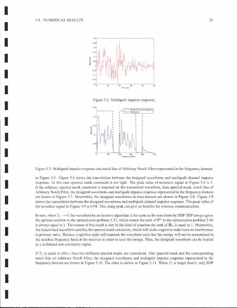
Figure 5.2 shows the multipath impulse response h(t) under investigation in this document and the energy of h(t) is normalized. Figure 5.3 shows the frequency domain representation hj(f) of h(t). Green notch line in Figure 5.3 shows the influence of Arbitrary Notch Filter at the receiver. Ts = 0.5ns, X/j = 100ns, Tp = 100ns and Tio + ^2 ~ 100ns- m me following presentation, the designed waveform, which is obtained by SDP and the rank of P* to the optimization problem 5.40 is not equal to 1, is called Waveform SDP Unverified; the designed waveform, which is obtained by SDP and the rank of P* to the optimization problem 5.40 is equal to 1 or which is obtained by SDP plus a randomized algorithm, is called Waveform SDP; the designed waveform, which is obtained by an iterative algorithm, is called Waveform by Iterative Algorithm.
If T/ —> 0, which means the integrator only captures one sample after ADC as the decision statistic, then spectral mask, notch line of Arbitrary Notch Filter, the designed waveforms and multipath impulse response represented in the frequency domain are shown in Figure 5.4. Meanwhile, the designed waveforms in time domain are shown
5.4. NUMERICAL RESULTS 35
Figure 5.2: Multhpath impulse response.
Multipath Impulse Response Notch Line
400 600 800 1000 Frequency (MHz)
Figure 5.3: Multipath impulse response and notch line of Arbitrary Notch Filter represented in the frequency domain.
in Figure 5.5. Figure 5.6 shows the convolution between the designed waveforms and multipath channel impulse response. In this case spectral mask constraint is not tight. The peak value of noiseless signal in Figure 5.6 is 1. If the arbitrary spectral mask constraint is imposed on the transmitted waveform, then spectral mask, notch line of Arbitrary Notch Filter, the designed waveforms and multipath impulse response represented in the frequency domain are shown in Figure 5.7. Meanwhile, the designed waveforms in time domain are shown in Figure 5.8. Figure 5.9 shows the convolution between the designed waveforms and multipath channel impulse response. The peak value of the noiseless signal in Figure 5.9 is 0.94. This sharp peak can give us benefits for wireless communication.
In sum, when Tj —> 0, the waveform by an iterative algorithm is the same as the waveform by SDP. SDP always gives the optimal solution to the optimization problem 5.35, which means the rank of P* to the optimization problem 5.40 is always equal to 1. The reason of this result is that in this kind of situation the rank of H0 is equal to 1. Meanwhile, the transmitted waveform satisfies the spectral mask constraint, which will make cognitive radio have no interference to primary radio. Besides, cognitive radio will transmit the waveform such that the energy will not be transmitted in the notched frequency band at the receiver in order to save the energy. Thus, the designed waveform can be treated as a wideband non-continuity signal.
If Tj is equal to 20ns, then two different spectral masks are considered. One spectral mask and the corresponding notch line of Arbitrary Notch Filter, the designed waveforms and multipath impulse response represented in the frequency domain are shown in Figure 5.10. The other is shown in Figure 5.11. When Tj is larger than 0, only SDP
36CHAPTER 5. WIDEBAND WAVEFORM OPTIMIZATION WITH ENERGY DETECTOR RECEIVER IN COGNITIV
- - Spectra! Mask - Notch Line Muttipatri Impulse Response Waveform by Iterative Algorithm
Waveform by SDP
400 Frequence (MHz)
Figure 5.4: Spectral mask, notch line of Arbitrary Notch Filter, the designed waveforms and multipath impulse response represented in the frequency domain when Tj —> 0.
Figure 5.5: Designed waveforms in the time domain when Tj —> 0.
can not guarantee the optimal solution at all times because the rank of P* to the optimization problem 5.40 can not be always equal to 1. In the first case, only SDP gives the optimal solution. But in the second case, the waveform obtained only by SDP violates the spectral mask constraint in some frequency points, and SDP plus a randomized algorithm gives the suboptimal solution.
5.5 Discussion
This chapter deals with wideband waveform optimization with energy detector in cognitive radio. Wideband wave- form is designed according to the optimization objective with the considerations of the spectral mask constraint at the transmitter and the influence of Arbitrary Notch Filter at the receiver. The optimization problem is formu- lated as QCQP. After relaxation, QCQP can be solved by using SDP plus a randomized algorithm. Meanwhile, a computationally-efficient iterative method is proposed to give the optimal solution for a special situation where the integrator only captures one sample after ADC as the decision statistic.
5.5. DISCUSSION 37
Waveform by Iterative Algorithm Wavafonn by SDP
100 Time (ns)
Figure 5.6: Convolution between the designed waveforms and the multipath impulse response when 77 —* 0.
400 600 Frequence (MHz)
Figure 5.7: Spectral mask, notch line of Arbitrary Notch Filter, the designed waveforms and multipath impulse response represented in the frequency domain when Tj —> 0.
Figure 5.8: Designed waveforms in the time domain when Tj —> 0.
38CHAPTER 5. WIDEBAND WAVEFORM OPTIMIZATION WITH ENERGY DETECTOR RECEIVER IN COGNITIV
MfY^A,---
Waveform by Iterative Algorithm Waveform by SDP
Time (ns)
Figure 5.9: Convolution between the designed waveforms and the multipath impulse response when T\ —> 0.
• • - Spectral Mask '•••• Notch Line Multipath Impulse Response Waveform by SDP Unverified
Waveform by SDP
400 600 Frequence (MHz)
Figure 5.10: Spectral mask, notch line of Arbitrary Notch Filter, the designed waveforms and multipath impulse response represented in the frequency domain when Tj is 20ns.
5 0.15
- Spectral Mask - Notch Line - Multipath Impulse Response - Waveform by SDP Unverified
Waveform by SDP
400 600 Frequence (MHz)
Figure 5.11: Spectral mask, notch line of Arbitrary Notch Filter, the designed waveforms and multipath impulse response represented in the frequency domain when T/ is 20ns.
Bibliography
[1] D. Singh, Z. Hu, and R. C. Qiu, "UWB Channel Sounding and Channel Characteristics in Rectangular Metal Cavity," in Proc of IEEE Southeastern Symposium, 2008.
[2] R. C. Qiu, C. Zhou, J. Q. Zhang, and N. Guo, "Channel Reciprocity and Time-Reversed Propagation for Ultra- Wideband Communications," in IEEE AP-S International Symposium on Antennas and Propagation, 2007.
[3] N. Guo, Z. Hu, A. S. Saini, and R. C. Qiu, "Waveform-level Precoding with Simple Energy Detector Receiver for Wideband Communication," in IEEE SSST'09, 2009.
[4] http://www.stan/ord.edu/ boyd/cvx/.
[5] A. Man and C. So, "Improved approximation bound for quadratic optimization problems with orthogonality constraints," in Proceedings of the Nineteenth Annual ACM-SIAM Symposium on Discrete Algorithms, pp. 1201— 1209, Society for Industrial and Applied Mathematics Philadelphia, PA, USA, 2009.
[6] A. Nemirovski, "Sums of random symmetric matrices and quadratic optimization under orthogonality con- straints," Mathematical Programming, vol. 109, no. 2, pp. 283-317, 2007.