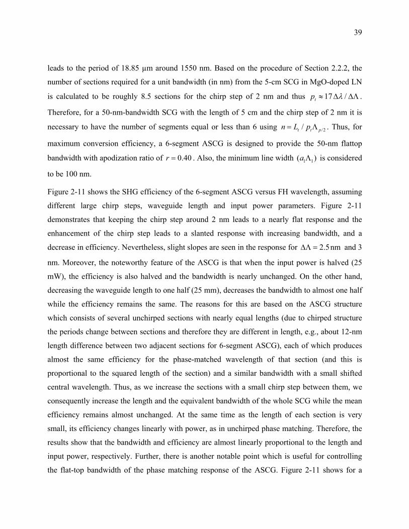
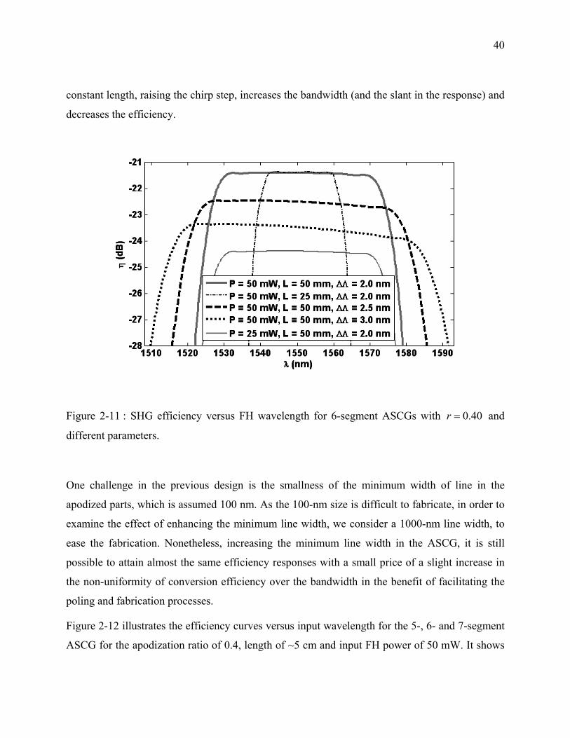
UNIVERSITÉ DE MONTRÉAL
BROADBAND QUASI-PHASE-MATCHED
WAVELENGTH CONVERTERS
AMIRHOSSEIN TEHRANCHI
DÉPARTEMENT DE GÉNIE ÉLECTRIQUE
ÉCOLE POLYTECHNIQUE DE MONTRÉAL
THÈSE PRÉSENTÉE EN VUE DE L’OBTENTION
DU DIPLÔME DE PHILOSOPHIÆ DOCTOR (Ph.D.)
(GÉNIE ÉLECTRIQUE)
JUIN 2010
© Amirhossein Tehranchi, 2010
UNIVERSITÉ DE MONTRÉAL
ÉCOLE POLYTECHNIQUE DE MONTRÉAL
Cette thèse intitulée:
BROADBAND QUASI-PHASE-MATCHED WAVELENGTH CONVERTERS
Présentée par: TEHRANCHI, Amirhossein
en vue de l’obtention du diplôme de : PHILOSOPHIAE DOCTOR
a été dûment acceptée par le jury d’examen constitué de :
M. CALOZ, Christophe, Ph.D., président
M. KASHYAP, Raman, Ph. D., directeur de recherche
M. WU, Ke, Ph.D., membre
M. HAUGEN, Harold K., Ph.D., membre
iii
To My Mother
(In Memory of My Father)
iv
ACKNOWLEDGMENTS
Greatest thanks to my supervisor, Prof. Raman Kashyap, who has been an invaluable source of
direction and support for my project. Without his encouragement, patience and guidance I could
never have accomplished this research and would never have gained what I did from it.
I would like to express my deep gratitude to Prof. K. Wu, the director of the Center of Research
in Radiofrequency Electronics (CREER) and Poly-Grames Research Center for his encouraging
and helpful suggestion on my research proposal in pre-doc exam.
I thank the other two members of my thesis defense committee, Prof. C. Caloz and Prof. H. K.
Haugen.
I would like to thank Prof. J. Yao, from the Microwave Photonics Lab, University of Ottawa, for
fruitful discussions on my research proposal in pre-doc exam.
I would like to acknowledge Prof. C.-Q. Xu, from the Department of Engineering Physics,
McMaster University, for helpful suggestion.
I am also thankful to Prof. N. Granpayeh from the Department of Electrical Engineering, K. N.
Toosi University of Technology, with whom I first started the research on nonlinear fiber optics
during my Master program.
I would like to thank my friends and colleagues in Advanced Photonics Concept Laboratory
(APCL) and Poly-Grames Research Center for their friendship, help and discussions.
I thank all friends specially Ebrahim Mortazy, Ramin Deban, Alireza Hassani, Hamidreza
Memarzadeh and Meenu Meenu for their encouragement and help.
I would like to thank my parents for the sacrifices they have made to help me pursue my interests,
my beloved sister Gita, and my dear fiancée Azadeh for love and support.
v
RÉSUMÉ
Cette thèse propose de nouveaux concepts dans la conversion de fréquence optique à large bande
dans les dispositifs à ondes guidées par quasi-accord de phase (QPM). Ces dernières années, la
QPM a été appliquée avec succès à l'aide des réseaux de domaines inversés en matériaux non
linéaires comme le niobate de lithium, en inversant le signe du deuxième ordre coefficient non
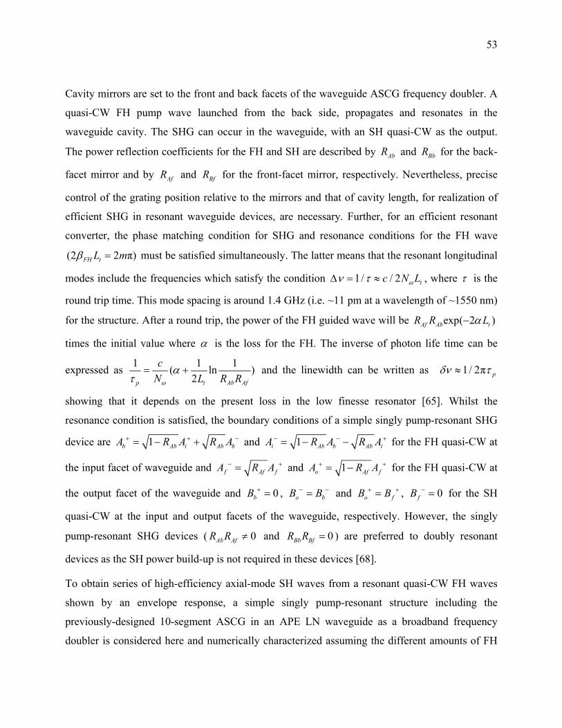
linéaire, pour tirer parti le plus fort coefficient non linéaire de la génération seconde harmonique
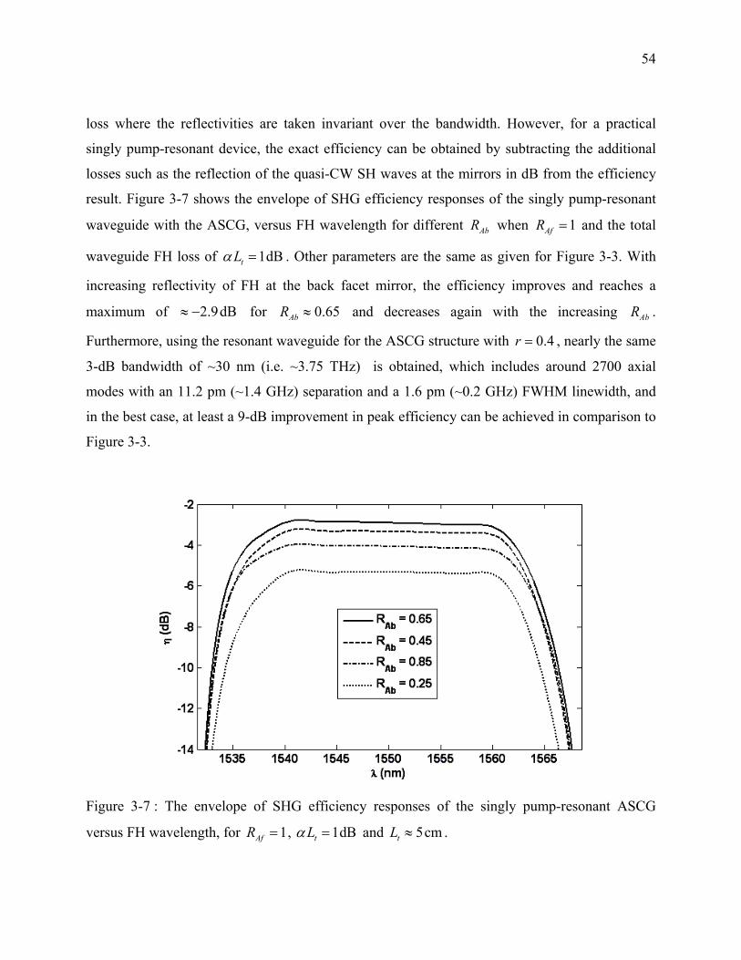
(SHG), la génération fréquence somme (SFG) et la génération fréquence différence (DFG).
Toutefois, une structure périodique a un impact négatif de limiter la bande passante.
Même si une structure apériodique contribue à augmenter la bande passante, elle apporte des
ondulations sur l’efficacité de conversion réduite, ce qui limite des applications. Néanmoins, une
modification de la structure basée sur le quasi-accord de phase semble prometteuse pour fournir
une large bande passante avec l'efficacité, et l'ondulation voulue. Il a été démontré pour la
première fois dans cette thèse que l'utilisation de la technique de l'apodisation des réseaux
apériodiques modifiée “apodized step-chirped gratings (ASCG)”, la bande passante d'un doubleur
de fréquence, basé sur la SHG en guide d'ondes du niobate de lithium, peut être élargie
volontairement et les ondulations peuvent être réduites (< ±0.05dB). Cela signifie également que
le dispositif peut être utilisé comme une source sur une large gamme de température. Il a été
vérifié que l'utilisation de l’ASCG, la bande passante large (> 50 nm) est suffisamment
contrôlable ; et la grande largeur de domaine et les étapes de chirp facilitent la fabrication des
dispositifs. Ces dispositifs à large bande peuvent premièrement être utilisés pour la conversion de
longueur d'onde variable dans les futurs réseaux optiques. Deuxièmement, ils mènent à l'avenir
pour la réalisation de convertisseurs de fréquence à haute efficacité pour les écrans.
Toutefois, l'efficacité de la SHG pour un dispositif avec l’ASCG est plus faible que celle du
réseau uniforme avec la même longueur. Il est démontré pour la première fois qu'il est possible
d'accroître l'efficacité de la SHG d'un dispositif avec l’ASCG, en utilisant un guide d'onde à faible
perte avec petite surface effective et avec la résonance des harmoniques fondamentales, ce qui
vi
permet de réaliser très efficace doubleurs de fréquence à large bande. Le dispositif efficace avec
l’ASCG permet également du doublement de fréquence d’une source à large bande pour des
nouvelles applications telles que la tomographie par cohérence optique (OCT), étant donné que la
résolution axiale pour la lumière à large bande en longueurs d'onde plus courte est plus
satisfaisante.
D'autres configurations modifiées ont également été proposées dans cette thèse, celles-ci
conduisent à élargir la bande passante et l'amélioration de l'efficacité des convertisseurs de
longueurs d'onde, fondées sur la génération de fréquence somme et différence en cascade (SFG +
DFG) avec un seul passage et doubles passages, qui utilisent quasi-accord de phase dans les
guides d'ondes du niobate de lithium. Néanmoins, en augmentant la différence de longueur
d'onde des pompes de la SFG + DFG en cascade, la bande passante peut être améliorée, mais
avec une variation notable sur la réponse de l’efficacité pour les plus grandes différences de
longueur d'onde des pompes, qui convertit le signal des canaux de façon inégale.
Deux solutions différentes à savoir, le désaccord de longueur d'onde d'une pompe et en utilisant
“step-chirped gratings (SCG)”, ont été proposées pour résoudre ce problème aux configurations
avec un seul passage et doubles passages. Il est montré que, si la longueur d'onde de la pompe ou
la période de la SCG est augmentée légèrement, les désaccords de phase de la SFG et la DFG
sont diminuées différemment, ce qui conduit à un aplatissement de la variation de la réponse.
Pour la première fois, il est démontré que, pour la même longueur et la même puissance,
l'amélioration de l'efficacité attendue, en raison de l'utilisation de la configuration avec les
doubles passages plutôt que le seul passage, est terminée pour une perte de guide d'ondes. En
outre, il est établi dans cette thèse que la configuration avec les doubles passages en utilisant
guide d'onde à faibles pertes, est capable d'améliorer l’efficacité de conversion, tandis que
l'aplatissement de la réponse de l'efficacité (< ±0.05dB) est accompli en augmentant le désaccord
de la longueur d'onde d'une pompe ou bien en utilisant la SCG.
Pour les systèmes du multiplexage en longueur d'onde (WDM) de l'avenir, le 3-dB bande passante
des convertisseurs de longueur d'onde doit être suffisamment large pour couvrir la fenêtre de
fibre optique à 1,55 µm. Il conviendra si les pompes sont fixées aux longueurs d'onde hors de la
fenêtre optique qui est au moins de 75 nm de large, tandis que nous avons besoin de réponses à
vii
plat avec l’efficacité de conversion élevée. Par conséquent, pour différents dispositifs avec un
seul passage et doubles passages, des schémas de conception pour le choix de la longueur de
guide d'ondes à faible perte et le choix de la puissance des pompes sont présentés pour atteindre
l'efficacité, l’ondulation et la bande passante souhaitée.
viii
ABSTRACT
This thesis proposes new concepts in broadband optical frequency conversion in quasi-phase
matched guided-wave devices. Quasi-phase matching (QPM) using domain-inverted gratings in
nonlinear materials such as lithium niobate (LN) by reversing the sign of the second-order
nonlinear coefficient, has been successfully applied in recent years to take advantage of the
highest nonlinear coefficient for second harmonic generation (SHG), sum frequency generation
(SFG) and difference frequency generation (DFG). Nevertheless, the periodic quasi-phase
matched structure has a negative impact by limiting the bandwidth of frequency up-conversion.
Although an aperiodic quasi-phase matched structure can help to increase the bandwidth, it may
cause ripples to appear in the reduced conversion efficiency response, which has detrimental
implications for applications. However, an engineered quasi-phase matched structure seems to be
a promising route to achieving a wide bandwidth with a desired efficiency, and tailored ripple. In
this dissertation, it has been demonstrated for the first time that using the technique of
apodization with chirped gratings, the bandwidth of frequency doublers based on SHG in lithium
niobate waveguides can be broadened at will, and the ripple damped out (< ±0.05dB) to be low
enough so as to be considered almost flat. A consequence of this technique is that the guided
wave device may be used as a source over a wide unregulated temperature range, for the first
time. It has been shown that using the apodized step-chirped gratings (ASCG) approach, the
wide spectral conversion efficiency profile (> 50 nm) is suitably controllable. The large domain-
widths and chirp-steps ease device manufacture. The impact of this design is clearly very high as
firstly, this broadband wavelength converter can be used for variable waveband wavelength
conversion in future all-optical networks, as the device based on the cascaded second harmonic
generation and difference frequency generation (SHG + DFG), should be a broadband frequency
doubler. Secondly, for displays it may lead to the realization of high-efficiency three-color
frequency converters that do not change in intensity, even without the use of temperature control.
ix
However, the SHG efficiency of an ASCG device is lower than that of the uniform grating with
the same length. It is shown for the first time that it is possible to increase the efficiency of an
ASCG device for broadband frequency doubling, by using a tight confinement in small-effective-
cross-section low-loss waveguides, and with the resonance of fundamental harmonics in a singly
pump-resonance waveguide. Another advantage of the efficient ASCG device is that it may allow
frequency doubling of ultra-broadband light for novel applications such as dual-band optical
coherence tomography (OCT) of tissues as the axial resolution length using wideband light at
shorter wavelengths is more satisfactory. This OCT may have the advantage of higher penetration
depth, providing additional phase and scattering information on the tissue sample examined.
The modified single-pass and double-pass configurations are also proposed in this dissertation
lead to bandwidth broadening and efficiency enhancement of waveband wavelength converters
based on quasi-phase matched cascaded sum frequency generation and difference frequency
generation (SFG + DFG) in LN waveguides. It has been shown that increasing the pump
wavelength difference in cascaded SFG + DFG devices, enhances the bandwidth, but with
noticeable variation in efficiency response for larger pump wavelength differences, leading to
uneven equal-input-power signal channel conversion.
Two different solutions have been suggested in this thesis to solve the problem in both single-
pass and double-pass configurations, namely, detuning of a pump wavelength, and using a few-
section step-chirped grating (SCG). It is shown that, if a pump wavelength is increasingly
detuned, the SFG and DFG phase-mismatch decreases differently which leads to flattening of the
conversion efficiency response. Alternatively, the period of a few-section SCG can also be
increased slightly to arrive at a similar result.
Also, for the first time, it is shown that for the same length and power, the efficiency
enhancement, expected due to the use of a double-pass configuration instead of a single-pass one,
is lost for a particular waveguide loss. Further, it is demonstrated that a double-pass configuration
with a low-loss waveguide is capable of improving the conversion efficiency while the efficiency
response flattening (< ±0.05dB) is accomplished by two schemes namely increasing the
wavelength detuning of one pump or alternatively using the SCG structure.
x
The role of these schemes is very important as wide waveband converters can be used for the
wavelength division multiplexing (WDM) systems, in which the 3-dB bandwidth of the device
should be broad enough to cover the 1.55 µm optical window. For this purpose, the pumps are set
at wavelengths out of the optical window which is 75-nm wide, whilst we obtain flat responses
with high conversion efficiency. For different single-pass and double-pass configurations using
pump detuning or the SCG, design diagrams for the choice of low-loss waveguide length, and the
assignment of pump powers of to achieve the desired efficiency, ripple and bandwidth are
presented.
xi
CONDENCÉ EN FRANÇAIS
Ces dernières années, il ya eu un grand intérêt pour les convertisseurs de longueur d'onde basée
sur le quasi-accord de phase (QPM) dans les guides d'ondes optiques non linéaires, car la
conversion de longueur d'onde peut être fait dans différentes bandes dans la région de la
transparence du milieu par une conception appropriée de domaines inversée.
La QPM a été appliquée avec succès à l'aide des réseaux de domaines inversés en matériaux non
linéaires, en inversant le signe du deuxième ordre coefficient non linéaire, pour tirer parti le plus
fort coefficient non linéaire de la génération seconde harmonique (SHG), la génération fréquence
somme (SFG) et la génération fréquence différence (DFG).
Aujourd'hui, le niobate de lithium est le matériel ferroélectrique dominant utilisé en optique non
linéaire intégrée. Construits en niobate de lithium polarisé périodiquement (PPLN) avec guides
d'ondes, des convertisseurs de longueur d'onde ont attiré une attention considérable en raison de
leurs excellentes propriétés. Ils ont été largement étudiés et trouvés de nombreuses applications
dans les communications et le traitement du signal dans la dernière décennie. Ils présentent à
haute vitesse, petite taille, haute efficacité, faible bruit, haute transparence pour le format de
modulation du signal.
Toutefois, une structure périodique a un impact négatif de limiter la bande passante. Même si une
structure apériodique contribue à augmenter la bande passante, elle apporte des ondulations sur
l’efficacité de conversion réduite, ce qui limite des applications. Néanmoins, une modification de
la structure basée sur le quasi-accord de phase semble prometteuse pour fournir une large bande
passante avec l'efficacité, et l'ondulation voulue.
Cependant, il ya eu un intérêt particulier pour réaliser des convertisseurs à large bande basés sur
la génération seconde harmonique dans les guides d'ondes non linéaires comme il ya plusieurs
applications. Pour la communication optique, une demande importante de la SHG à large bande
xii
est dans la conversion variable de longueur d'onde basée sur la génération seconde harmonique et
la génération de la fréquence différence en cascade (SHG + DFG) qui a besoin d'un doubleur de
fréquence à large bande. Dans les anciens schémas, la bande passante de la pompe est étroite et
donc les signaux peuvent être convertis en longueurs d'onde limitée qui se traduisent par
l'inflexibilité du convertisseur variable de longueur d'onde.
Une autre application est dans la transformation des signaux optiques ultrarapides dans lequel le
problème est associé à générer des impulsions ultra-courtes pour la seconde harmonique, aux
réseaux périodiques de PPLN. Aussi, le convertisseur à large bande est bon pour la tomographie
par cohérence optique (OCT), une technique utilisée pour diagnostiquer divers troubles
médicaux.
Dans ce cas, dispositifs à large bande agirent comme une source de la lumière à large bande pour
des longueurs d'onde plus courte. La raison de l'utilisation de la source à large bande dans un
système OCT est la relation inverse entre la largeur de bande de la lumière et de la résolution
axiale. La source de lumière à large bande dans le proche infrarouge est utilisée parce que la
résolution axiale est aussi proportionnelle au carré de la longueur d'onde de la lumière.
Néanmoins, le problème lié à la conversion de longueurs d'onde fondée sur la SHG dans PPLN
est la bande passante étroite, comme la bande passante dépend de l'inverse de la longueur du
réseau de PPLN. Une solution simple consiste à utiliser un guide d'ondes courtes de PPLN pour
obtenir une bande passante large. Toutefois, cela ne fonctionne pas ainsi que d'atteindre une
efficacité raisonnable, il a besoin de très forte puissance d'entrée qui ne peut pas être tolérée par
le guide d'ondes dans PPLN.
Ainsi, le réseau à pas variable a été proposé d'élargir la bande passante en changeant la période
des domaines inversés en fonction de la longueur. Grâce à cette structure, élargissement de la
bande passante de conversion est atteinte, mais avec une réponse fluctuée qui n'est pas acceptable
pour les applications précitées. Il est également important qu'elle présente une bande passante
plus large pour l'acceptation de la température que le réseau périodique (à pas constant) et fournit
une plus grande stabilité du doublement de fréquence.
xiii
Toutefois, il existe trois problèmes en utilisant les réseaux à pas variable. Le premier problème
pour la réalisation d'un dispositif à large bande est l'étroitesse du changement de période. Pour le
réseau avec des variations linéaires de changement de la période qui est appelé linear-chirp
grating (LCG), il est généralement d'environ 100 picomètres ou moins pour un convertisseur avec
quelques nanomètres de largeur de bande.
Nous allons montrer pour la première fois que l'utilisation du réseau avec des variations comme
étape pour le changement de la période qui est appelé step-chirp grating (SCG), il est possible
d'augmenter le changement de période pour la commodité de fabrication alors que la bande
passante et l'efficacité restent presque les mêmes par rapport à la LCG.
Le deuxième problème est la fluctuation considérable sur la réponse de l'efficacité de la LCG et
SCG. La méthode pour aplatir la réponse de la SHG est d'utiliser apodisation. Ici, nous pouvons
le faire en changeant le rapport entre la largeur du créneau et la période dans des régions
polarisées, qui contribue à éliminer les ondulations et obtenir des réponses à plat.
Le troisième problème est lié à l'efficacité médiocre de la SHG pour la SCG apodisée (ASCG).
L'efficacité peut être augmentée pour guides d'ondes avec la petite surface effective avec ou sans
résonance. Néanmoins, il est démontré pour la première fois que l'utilisation du guide d'ondes
avec la résonance de la pompe, forte amélioration de l'enveloppe de la réponse de l'efficacité de
la SHG à large bande est possible.
Dans cette thèse, l'ingénierie des réseaux ou des domaines inversée, dans les guides d'ondes à
faible perte qui est fabriqué par la diffusion du titane dans le niobate de lithium (Ti:LN), est
présentée de telle manière à élargir la bande passante de la SHG de façon significative. Une
formule de conception est proposée pour la première fois, de décider combien de segments on
devrait utiliser comme une règle de conception, qui est dépendante de la bande passante requise.
En outre, nous considérons une méthode de l'apodisation pour aplatir la bande passante de la
SHG par la conception de l'augmentation et la diminution de domaines inversés dans les réseaux.
Il a été démontré pour la première fois dans cette thèse que l'utilisation de la technique de
l'ASCG, la bande passante d'un doubleur de fréquence, basé sur la SHG en guide d'ondes du
xiv
niobate de lithium, peut être élargie volontairement et les ondulations peuvent être réduites
(< ±0.05dB). Cela signifie également que le dispositif peut être utilisé comme une source sur une
large gamme de température. Il a été vérifié que l'utilisation de l’ASCG, la bande passante large
(> 50 nm) est suffisamment contrôlable; et la grande largeur de domaine et les étapes de chirp
facilitent la fabrication des dispositifs.
Néanmoins, le concept proposé de l’ASCG peut être appliqué au quasi-accord de phase à large
bande pour les autres matériaux non linéaires, avec ou sans guide d'ondes. Enfin, la bande
passante de conversion de 50 nm (et même plus) peut être obtenu avec la conception spéciale de
l’ASCG avec le 1-µm de largeur de ligne, pour nous fournir une réponse uniforme et de faciliter
le processus de la fabrication.
Il est démontré que l'efficacité de la SHG pour l’ASCG dans guides d'ondes (Ti:LN) peut être
améliorée en utilisant des guides d'ondes avec la petite surface effective. Pour atteindre cet
objectif, guides d'ondes réalisés par échange protonique recuit (APE) sont utilisés en raison de la
possibilité d'une différence d'indice plus élevé, des modes bien confinés en raison des petites
surfaces des champs des modes.
En plus, pour la résonance de la pompe, il est démontré que, pour la pompe quasi continue il est
possible d'augmenter efficacement l'enveloppe de l'efficacité de la conversion des modes de
résonance axiale (surtout pour les faibles pertes), tandis que la bande passante de conversion reste
à peu près les mêmes. Les valeurs optimisées de réflectivité pour une facette arrière et une
puissance d'entrée ont aussi été présentées pour atteindre l'efficacité maximale, pour les pertes
des guides d'ondes.
Il ya eu aussi un grand intérêt pour le développement des convertisseurs de longueur d'onde à
large bande pour la bande de communication (waveband) basée sur χ(2) en cascade, à savoir
(SHG + DFG) en cascade, et la génération de la fréquence somme et différence en cascade
(SFG + DFG) pour le futur système du multiplexage en longueur d'onde (WDM).
Pour les systèmes du WDM de l'avenir, le 3-dB bande passante des convertisseurs de longueur
d'onde doit être suffisamment large pour couvrir la fenêtre de fibre optique à 1,55 µm. Il
xv
conviendra si les pompes sont fixées aux longueurs d'onde hors de la fenêtre optique qui est au
moins de 75 nm de large, tandis que nous avons besoin de réponses à plat avec l’efficacité de
conversion élevée.
L'avantage le plus notable des dispositifs basés sur χ(2) en cascade est la large couverture de
longueur d'onde pendant que la pompe, signal et le signal converti sont dans la même bande. Ils
peuvent offrir une bande passante large et une haute efficacité avec la puissance modérée de la
pompe.
En plus de la fonction de conversion de longueurs d'onde, ces dispositifs peuvent effectuer des
différents traitements de signaux optiques ultrarapides comme la commutation tout-optique,
offrant des possibilités d'applications pour les réseaux photoniques ultrarapide basée sur le
multiplexage temporel optique (OTDM).
Les convertisseurs de longueur d'onde fondée sur χ(2) en cascade également offrent une variété de
possibilités pour des applications dans le traitement du signal y compris la génération de
millimeter-wave/THz et la radio sur fibre.
La DFG et SHG + DFG en guide d'ondes dans PPLN, a déjà été montrée à la fois théoriquement
et expérimentalement avec plusieurs applications. Pour la conversion de longueurs d'onde dans
une bande de communication, un avantage de la SHG + DFG en cascade par rapport à la DFG
est qu'une pompe avec la longueur d'onde dans la même bande du signal peut être utilisée.
Toutefois, il est difficile d'obtenir une haute efficacité avec une pompe de faible puissance dans la
SHG + DFG en cascade avec un seul passage.
Pour résoudre ce problème, la SHG + DFG en cascade avec des doubles passages est une bonne
technique pour accroître l'efficacité, mais avec une petite perte de bande passante. Néanmoins,
l'inconvénient de la SHG + DFG, par exemple pour les systèmes WDM, est que plusieurs canaux
doivent être sacrifiés parce que la longueur d'onde de la pompe doit être fixée au centre de la
bande de conversion occupant les places des canaux possibles.
Une technique intéressante de conversion de longueurs d'onde fondée sur la SFG + DFG en
cascade, a été démontrée théoriquement et pratiquement dans les guides d'ondes PPLN et a
xvi
trouvé de vastes applications y compris la conversion de longueur d'onde à large bande, la
conversion des canaux sélectionnés et multiples et la conversion de format. Pourtant, la bande
passante de 3 dB de ces convertisseurs devrait être suffisamment large pour couvrir la fenêtre
optique en 1,55 µm. Il conviendra pour des applications pratiques si nous pouvons définir les
pompes hors de la fenêtre optique qui est au moins 75 nm, alors que nous avons besoin de
réponses à plat avec l'efficacité élevée de conversion.
En utilisant cette technique, en augmentant la différence de longueur d'onde de pompe, la bande
passante pourrait être améliorée. Toutefois, la moyenne de l'efficacité de conversion dépend de la
longueur d'onde de la pompe et celle-ci est diminuée en augmentant la différence de longueur
d'onde de pompe.
Deux solutions différentes à savoir, le désaccord de longueur d'onde d'une pompe et en utilisant
la SCG, ont été proposées pour résoudre ce problème. Pour compenser la réduction de l'efficacité,
la SFG + DFG en cascade avec des doubles passages a été proposée qui est également capable de
filtrer les longueurs d'onde de pompe résiduelle à la sortie.
Cependant, pour la longueur d'onde de pompe, le quasi-accord de phase de la SFG est
parfaitement respecté tandis que le désaccord de phase de la DFG est grand lorsque le signal est
loin de la pompe. Ainsi, le désaccord augmente la variation de la conversion pour la grande
différence de la longueur d'onde des pompes, qui convertit le signal des canaux de façon inégale.
Bien que la SFG + DFG en cascade a été principalement étudiée, la recherche sur la façon de
définir exactement les pompes ou encore la façon de concevoir les réseaux pour améliorer les
propriétés de conversion reste toujours et il est de grande importance. Les solutions au problème
sont proposées pour la première fois, en dispositifs avec un seul passage et des doubles passages
en utilisant le désaccord de la longueur d'onde de pompe, ou en utilisant alternativement la SCG.
Nous montrons que, si la longueur d'onde de la pompe ou l'étape de chirp de la SCG est
légèrement augmentée, les désaccords de phase de la SFG et DFG sont réduits ce qui conduit à
un aplatissement de la variation de la réponse.
xvii
Dans cette thèse, nous évaluons et comparons numériquement les propriétés de la SHG + DFG et
SFG + DFG en cascade lorsque la différence de longueur d'onde de pompe est
0 nm et 75 nm, respectivement, et nous montrons que pour la même longueur, l'adoption de la
SFG + DFG améliore encore la bande passante avec une légère diminution de l'efficacité et une
augmentation de l'ondulation.
En outre, nous présentons les critères de sélection de la longueur du guide d'ondes et la puissance
de pompe pour obtenir l'efficacité, l'ondulation et la bande passante requise. Nous montrons que
l’augmentation du désaccord de longueur d’onde d’une pompe, dans le dispositif avec le seul
passage, supprime l'ondulation avec une pénalité sur l'efficacité moyenne.
L'introduction de la structure de la SCG avec une conception appropriée, elle offre presque la
même bande passante et de la planéité avec moins de pénalité de l'efficacité par rapport au
dispositif avec le désaccord de la pompe. Nous aussi présentons les diagrammes de conception du
dispositif avec le seul passage pour la sélection de la longueur et la puissance pour obtenir
l'efficacité, l'ondulation et la bande passante requise.
En plus, les propriétés de la SHG + DFG et SFG + DFG en cascade avec des doubles passages
sont évaluées et comparées numériquement lorsque la différence de longueur d'onde de pompe
est de 0 nm et 75 nm, respectivement. Il est démontré que, pour la même longueur de guide
d'ondes à faible perte, l'adoption des dispositifs avec des doubles passages, en utilisant le
désaccord de la pompe ou alternativement de la SCG, améliore encore les performances
d'efficacité avec une petite réduction de la bande passante, par rapport à celles des dispositifs
avec un seul passage.
Il est démontré que, pour la même longueur et la puissance, l'amélioration de l'efficacité attendue,
en raison de l'utilisation des dispositifs avec des doubles passages au lieu d'un seul passage, est
finalement interrompue pour une perte de guide d'ondes. Nous présentons les diagrammes de la
conception des dispositifs avec des doubles passages, pour le choix de la longueur et la puissance
pour obtenir l'efficacité, l'ondulation et la bande passante nécessaire.
xviii
LIST OF PUBLICATION RELATED TO THE DISSERTATION
Journals
1. A. Tehranchi, and R. Kashyap, “Wideband wavelength conversion using double-pass cascaded
χ(2) : χ(2) interaction in lossy waveguides,” Opt. Commun., vol. 283, pp. 1485-1488, 2010.
2. A. Tehranchi, and R. Kashyap, “Response flattening of efficient broadband wavelength
converters based on cascaded sum- and difference frequency generation in periodically poled
lithium niobate waveguides,” IEEE J. Quantum Electronics, vol. 45, 9 pp. 1114-20, 2009.
3. A. Tehranchi, and R. Kashyap, “Efficient wavelength converters with flattop responses based
on counterpropagating cascaded SFG and DFG in low-loss QPM LiNbO3 waveguides,” Optics
Express, vol. 17, 21, pp. 19113–19119, 2009.
4. A. Tehranchi, and R. Kashyap, “Improved cascaded sum and difference frequency generation-
based wavelength converters in low-loss quasi-phased-matched lithium niobate waveguides,”
Applied Optics, vol. 48, 31, pp. G143-7, 2009.
5. A. Tehranchi, and R. Kashyap, “Novel designs for efficient broadband frequency doublers
using singly pump-resonant waveguide and engineered chirped gratings,” IEEE J. Quantum
Electronics, vol. 45, 2, pp. 187-94, 2009.
6. A. Tehranchi, and R. Kashyap, “Engineered gratings for flat broadening of second-harmonic
phase-matching bandwidth in MgO-doped lithium niobate waveguides,” Optics Express, vol. 16,
23, pp. 18970-75, 2008.
7. A. Tehranchi, and R. Kashyap, “Design of novel unapodized and apodized step-chirped quasi-
phase matched gratings for broadband frequency converters based on second harmonic
generation,” IEEE J. Lightwave Technol., vol. 26, 3, pp. 343-49, 2008.
xix
Patents
1. R. Kashyap, and A. Tehranchi, “Design of novel unapodized and apodized step-chirped quasi-
phase matched gratings for broadband frequency converters based on second harmonic
generation,” USPTO Application # 61233230, Filed on August 2009.
Short Technical Reviews
1. A. Tehranchi, and R. Kashyap, “Efficient wavelength conversion with flattop response based
on double-pass cascaded χ(2) in periodically poled LiNbO3 waveguides,” Photons, vol. 7, 2, pp.
23-5, 2010.
Conferences (Presenter underlined)
1. A. Tehranchi, and R. Kashyap, “Pump-detuned double-pass cSFG/DFG-based wavelength
converters in lossy PPLN waveguides,” In Proceedings of 2010 Bragg Gratings, Photosensitivity
and Poling in Glass Waveguides (BGPP) and Nonlinear Photonics (NP), NTuC21, 21-24 June,
2010, Karlsruhe, Germany. (Received a CIPI travel award)
2. A. Tehranchi, and R. Kashyap, “Flattop broadband wavelength converters based on double-
pass cascaded SFG + DFG in quasi-phase matched waveguides,” In IEEE Proceedings of the 22nd
Annual Lasers and Electro Optics Society (LEOS) Meeting, ThY4, pp. 819-20, October 4-8,
2009, Antalya, Turkey.
3. A. Tehranchi, and R. Kashyap, “High-efficiency pump-resonant quasi-phase-matched
frequency doublers with flat broadband responses,” In Proceedings of the International
Symposium on SPIE Photonic Devices + Applications, vol. 7420, August 2-6, 2009, San Diego,
USA. (Received an SPIE scholarship)
4. Invited Paper: R. Kashyap, A. Tehranchi, and C.-Q. Xu, “Efficient broadband frequency
conversion using engineered apodized χ(2) gratings and fundamental harmonic resonance,” In
Proceedings of the 14th OptoElectronics and Communications Conference (OECC 2009),TuG6,
13-17 July, Hong Kong.
xx
5. A. Tehranchi, and R. Kashyap, “Analysis of improved cascaded SFG+DFG wavelength
converter in quasi-phase matched lithium niobate waveguide,” In Proceedings of Photonics 2008
Conference, WC2.3, 13-17 December, New Delhi, India.
6. A. Tehranchi, and R. Kashyap, “Novel step-chirped quasi-phase matched gratings for flatly
broadband frequency doublers with high efficiency in nonlinear-optic waveguides,” In
Proceedings of XXIXth General Assembly of the International Union of Radio Science (URSI
2008), D02a.5, 7-16 August 2008, Chicago, USA. (Won the best student paper award from
the Canadian National Committee)
7. A. Tehranchi, and R. Kashyap, “A new design of apodized step-chirped gratings for broadband
wavelength converters,” In Proceedings of 2007 Bragg Gratings, Photosensitivity and Poling in
Glass Waveguides (BGPP) and Nonlinear Photonics (NP), JMD30, 2-6 September, Quebec City,
Canada.
LIST OF RELATED SCHOLARSHIPS AND AWARDS
The 2010 John Kiel Scholarship ($10,000) from SPIE - The International Society for Optics and
Photonics- in May 2010.
The Travel Award from the Canadian Institute for Photonic Innovations (CIPI) for attendance at
NP in June 2010.
The SPIE Scholarship in Optical Science and Engineering in May 2009.
The Charles Baskin Scholarship from École Polytechnique de Montréal in February 2009.
The URSI Student Award from the Canadian National Committee (CNC) of the International
Union of Radio Science (URSI) in May 2008.
xxi
TABLE OF CONTENTS
ACKNOWLEDGMENT………………….…………………………….…….…………….…...iv
RÉSUMÉ……………………………………..….………………………………….………….…v
ABSTRACT…………………………………..………..………………………………….……viii
CONDENCÉ EN FRANÇAIS………………….…….…………………………………..…..…xi
LIST OF PUBLICATIONS……………………………………..………………….….…......xviii
TABLE OF CONTENTS…………………………………….………..………………….……xxi
LIST OF TABLES…………..…………………………………………………..…………….xxiv
LIST OF FIGURES………………..………………………………………….….….………...xxv
LIST OF ACRONYMS………………..……………………………………………..……......xxx
LIST OF SYMBOLS AND NOTATIONS…………….………………...…………...……..xxxii
CHAPTER 1 INTRODUCTION .............................................................................................. 1
1.1 Motivation ......................................................................................................................... 1
1.2 Second-order NLO wavelength conversion ...................................................................... 1
1.3 Phase matching .................................................................................................................. 3
1.3.1 Birefringent phase matching ........................................................................................... 4
1.3.2 Quasi-phase matching ..................................................................................................... 6
1.4 Poling and waveguide fabrication in LN .......................................................................... 8
1.5 SHG, DFG and SFG in PPLN waveguide ........................................................................ 9
1.6 Wavelength conversion using broadband SHG (frequency doubling) ........................... 12
1.7 Waveband wavelength conversion using broadband cascaded χ(2) ................................. 15
xxii
1.8 Overview of the dissertation ........................................................................................... 17
CHAPTER 2 BANDWIDTH BROADENING AND FLATENNING OF QUASI-PHASE
MATCHED SHG USING APODIZED STEP-CHIRPED GRATING .................................. 20
2.1 Overview ......................................................................................................................... 20
2.2 Modeling of step-chirped grating .................................................................................... 21
2.2.1 Bandwidth of a section in a step-chirped grating .......................................................... 24
2.2.2 Design considerations of step-chirped grating .............................................................. 25
2.3 Apodized chirped gratings .............................................................................................. 30
2.3.1 Design of step-chirped grating with apodization .......................................................... 32
2.4 Few-segment ASCGs in MgO-doped LN ....................................................................... 38
2.5 Conclusion ....................................................................................................................... 43
CHAPTER 3 EFFICIENCY ENHANCEMENT OF BROADBAND QUASI-PHASE
MATCHED SHG USING SMALL EFFECTIVE-CROSS-SECTION WAVEGUIDE AND
SINGLY PUMP-RESONANCE .................................................................................................. 44
3.1 Overview ......................................................................................................................... 44
3.2 Design of efficient broadband SHG using APE waveguide ........................................... 45
3.3 Design of efficient broadband SHG using pump-resonant waveguides ......................... 52
3.4 Conclusion ....................................................................................................................... 59
CHAPTER 4 BANDWIDTH BROADENING BY SINGLE-PASS CASCADED SFG +
DFG AND RESPONSE FLATENNING USING PUMP TUNING AND SCG ..................... 60
4.1 Overview ......................................................................................................................... 60
4.2 Single-pass cascaded SFG + DFG .................................................................................. 61
4.2.1 Bandwidth broadening .................................................................................................. 63
4.2.2 Response flattening ....................................................................................................... 66
xxiii
4.3 Conclusion ....................................................................................................................... 77
CHAPTER 5 ENHANCEMENT OF CONVERSION EFFICIENCY BY DOUBLE-
PASS CASCADED SFG + DFG AND RESPONSE FLATENNING USING PUMP
TUNING AND SCG ..................................................................................................................... 78
5.1 Overview ......................................................................................................................... 78
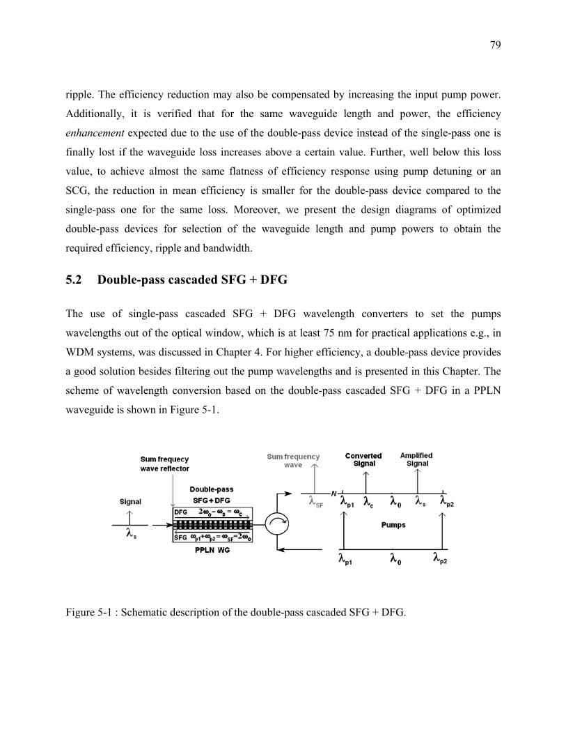
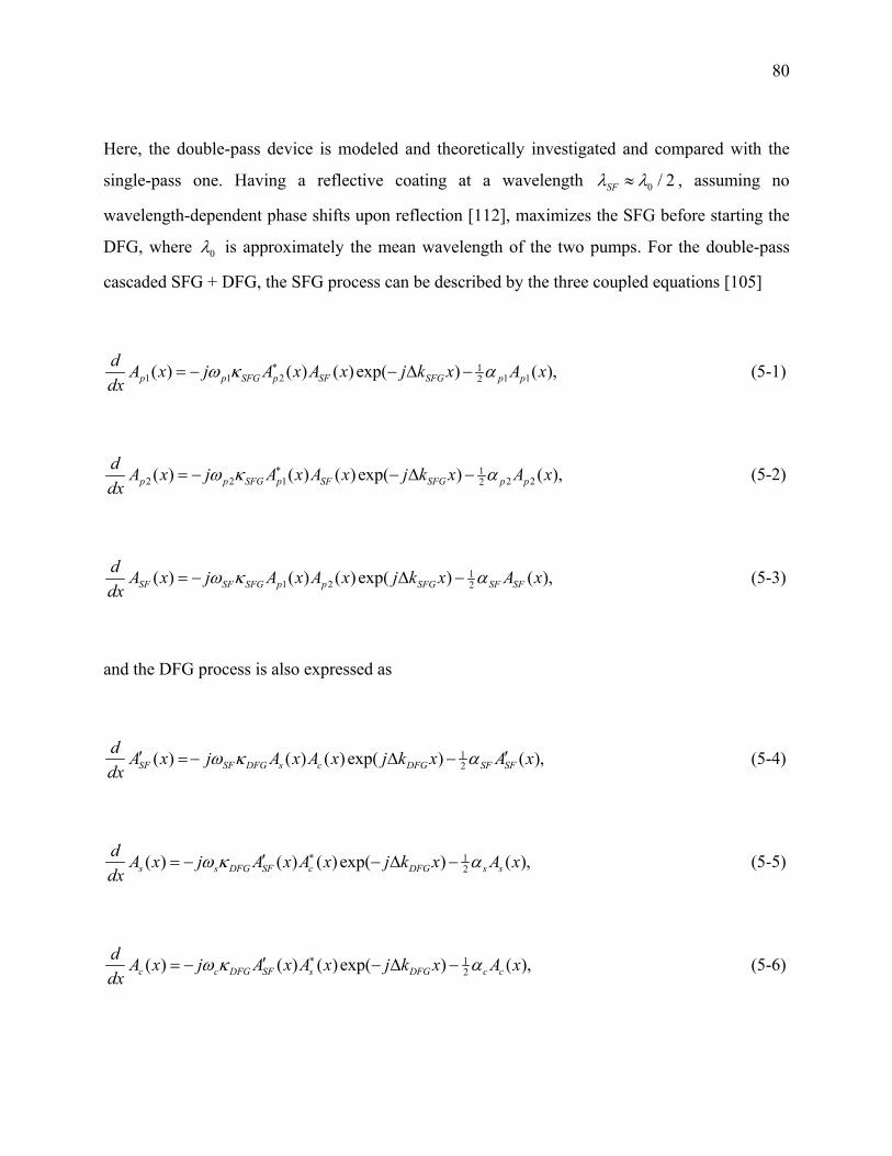
5.2 Double-pass cascaded SFG + DFG ................................................................................. 79
5.2.1 Enhancement of conversion efficiency ......................................................................... 81
5.2.2 Response flattening ....................................................................................................... 84
5.3 Comparison of double-pass and single-pass configurations ........................................... 91
5.3.1 Efficiency versus waveguide loss ................................................................................. 91
5.3.2 Uniform-grating device (with pump detuning) versus 3-section SCG device .............. 95
5.4 Conclusion ....................................................................................................................... 96
CHAPTER 6 CONCLUSIONS ............................................................................................... 97
6.1 Thesis overview .............................................................................................................. 97
6.2 Direction for future work .............................................................................................. 100
xxiv
LIST OF TABLES
Table 2-1 : Design parameters for different engineered chirped gratings to achieve almost the
same mean efficiency and bandwidth. ........................................................................................... 42
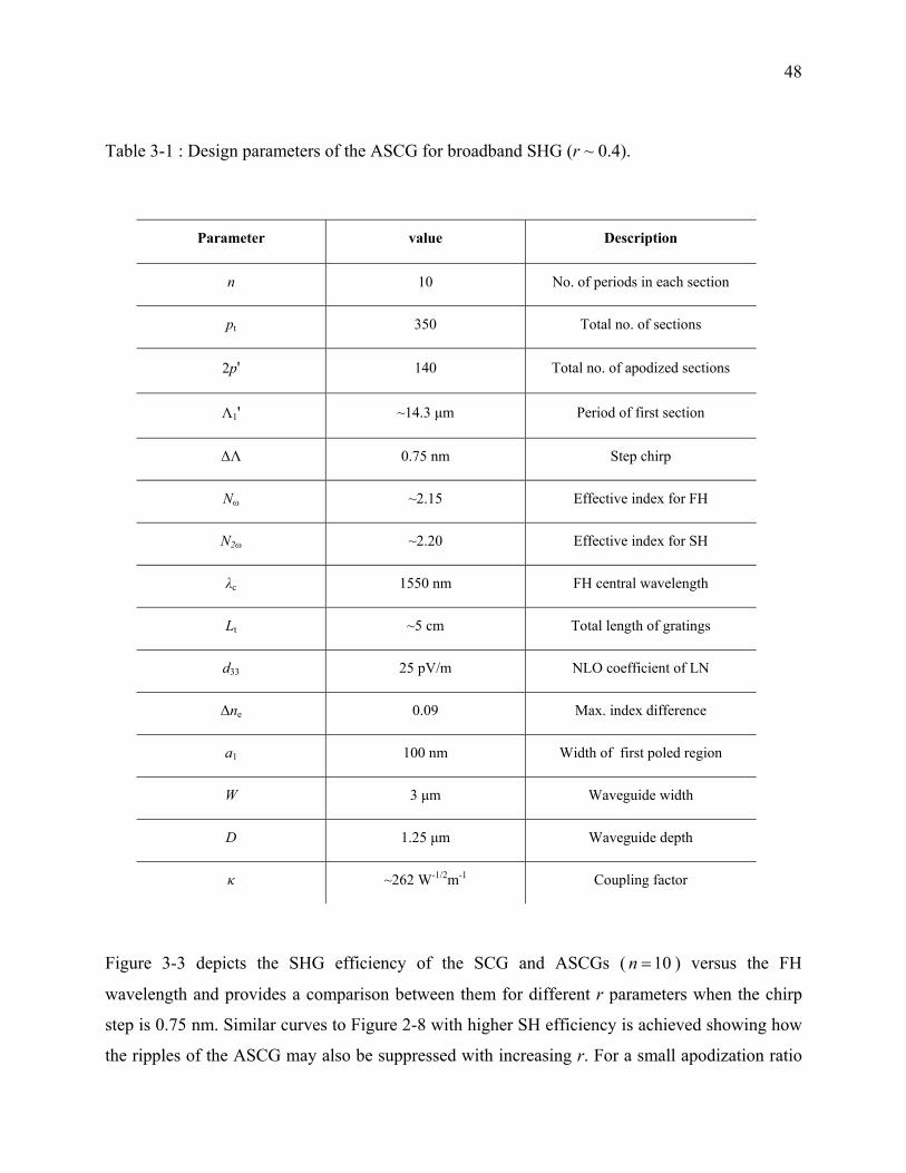
Table 3-1 : Design parameters of the ASCG for broadband SHG (r ~ 0.4). .................................. 48
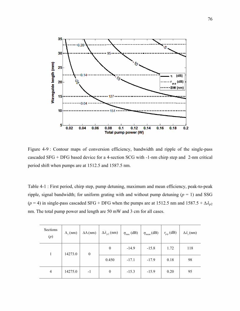
Table 4-1 : First period, chirp step, pump detuning, maximum and mean efficiency, peak-to-peak
ripple, signal bandwidth; for uniform grating with and without pump detuning (p = 1) and SSG
(p = 4) in single-pass cascaded SFG + DFG when the pumps are at 1512.5 nm and 1587.5 + p2
nm. The total pump power and length are 50 mW and 3 cm for all cases. .................................... 76
Table 5-1 : First period, chirp step, pump detuning, maximum and mean efficiency, peak-to-peak
ripple, signal bandwidth; for uniform grating with and without pump detuning (p = 1) and SSG
(p = 2) in double-pass cascaded SFG + DFG when the pumps are at 1512.5 nm and 1587.5 + p2
nm. The total pump power and length are 50 mW and 3 cm for all cases. .................................... 90
Table 5-2 : Comparison of the mean efficiency, ripple and bandwidth; for uniform grating with
and without pump detuning (p = 1) and SCG (p = 3) of single-pass and double-pass cascaded
SFG + DFG schemes when the pumps are at 1512.5 nm and 1587.5 + p2 nm. The total pump
power and length are 50 mW and 3 cm for all cases. ..................................................................... 95
xxv
LIST OF FIGURES
Figure 1-1 : A schematic view for using the LN crystal birefringence to obtain phase matching. .. 5
Figure 1-2 : SH power versus crystal length for (a) phase matching and (b) no phase matching
and (c) quasi-phase matching schemes. ........................................................................................... 7
Figure 1-3 : A narrowband frequency doubler based on a uniform PPLN waveguide. ................... 9
Figure 1-4 : (a) DFG scheme and (b) cascaded SHG + DFG scheme for broadband wavelength
conversion. ..................................................................................................................................... 11
Figure 1-5 : Concepts of SHG bandwidth broadening in quasi-phase matched devices. .............. 14
Figure 2-1 : Scheme of a domain-inverted SCG. The plus and minus signs refer to the sign of χ(2)
in gray and white regions, respectively. ......................................................................................... 22
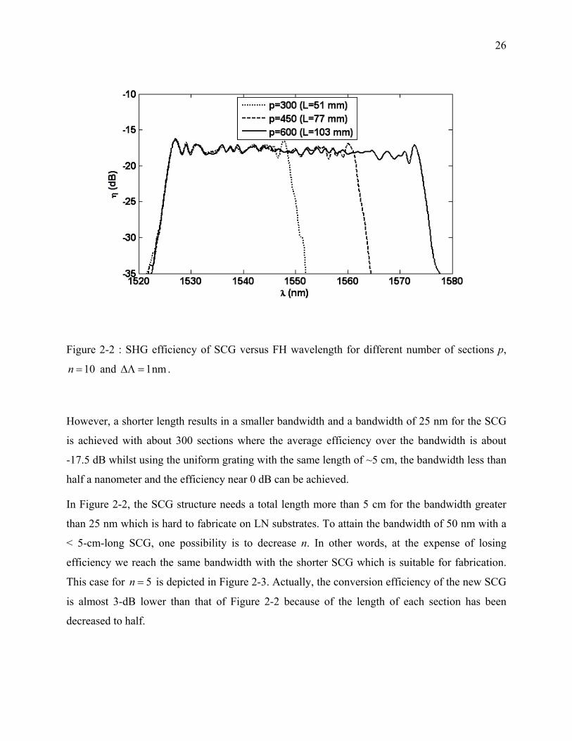
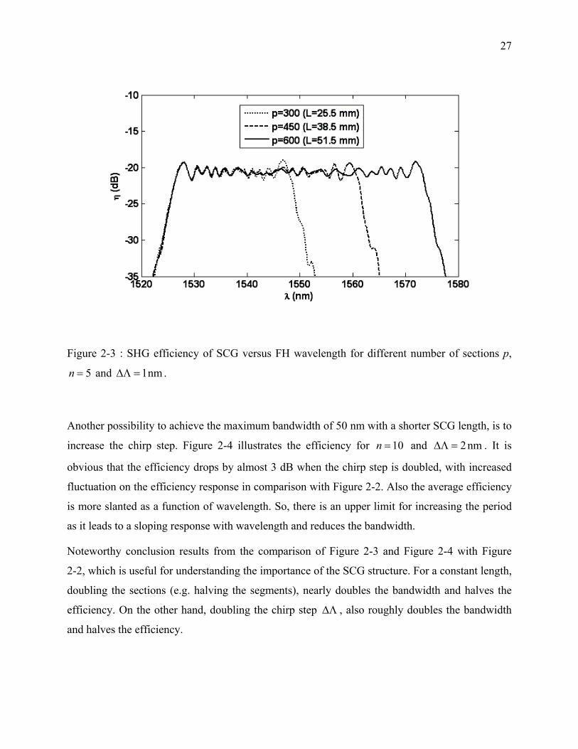
Figure 2-2 : SHG efficiency of SCG versus FH wavelength for different number of sections p,
10n and 1nm . ................................................................................................................... 26
Figure 2-3 : SHG efficiency of SCG versus FH wavelength for different number of sections p,
5n and 1nm . ..................................................................................................................... 27
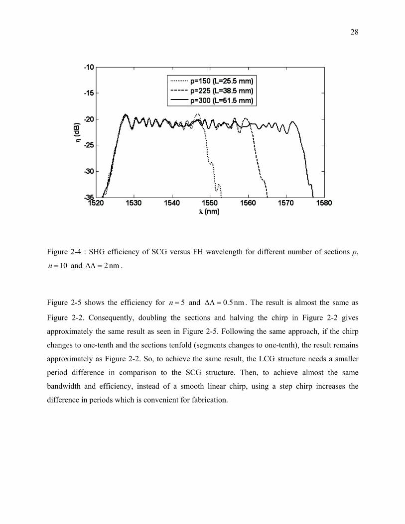
Figure 2-4 : SHG efficiency of SCG versus FH wavelength for different number of sections p,
10n and 2nm . .................................................................................................................. 28
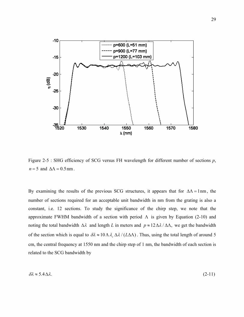
Figure 2-5 : SHG efficiency of SCG versus FH wavelength for different number of sections p,
5n and 0.5nm . ................................................................................................................. 29
Figure 2-6 : Model of imposed quasi-phase matched grating structures with (a) increasing and (b)
decreasing parts of inverted domains. The ASCG structure begins with (a) at the left side and
ends with (b) at the right side of the SCG structure shown in Figure 2-1 where 1 p and
1 p . ................................................................................................................................ 34
xxvi
Figure 2-7 : Different apodization functions versus length for different apodization ratios, with
=3000tnp . ...................................................................................................................................... 35
Figure 2-8 : SHG efficiency of SCG and ASCG for the different apodization ratios with 10n ,
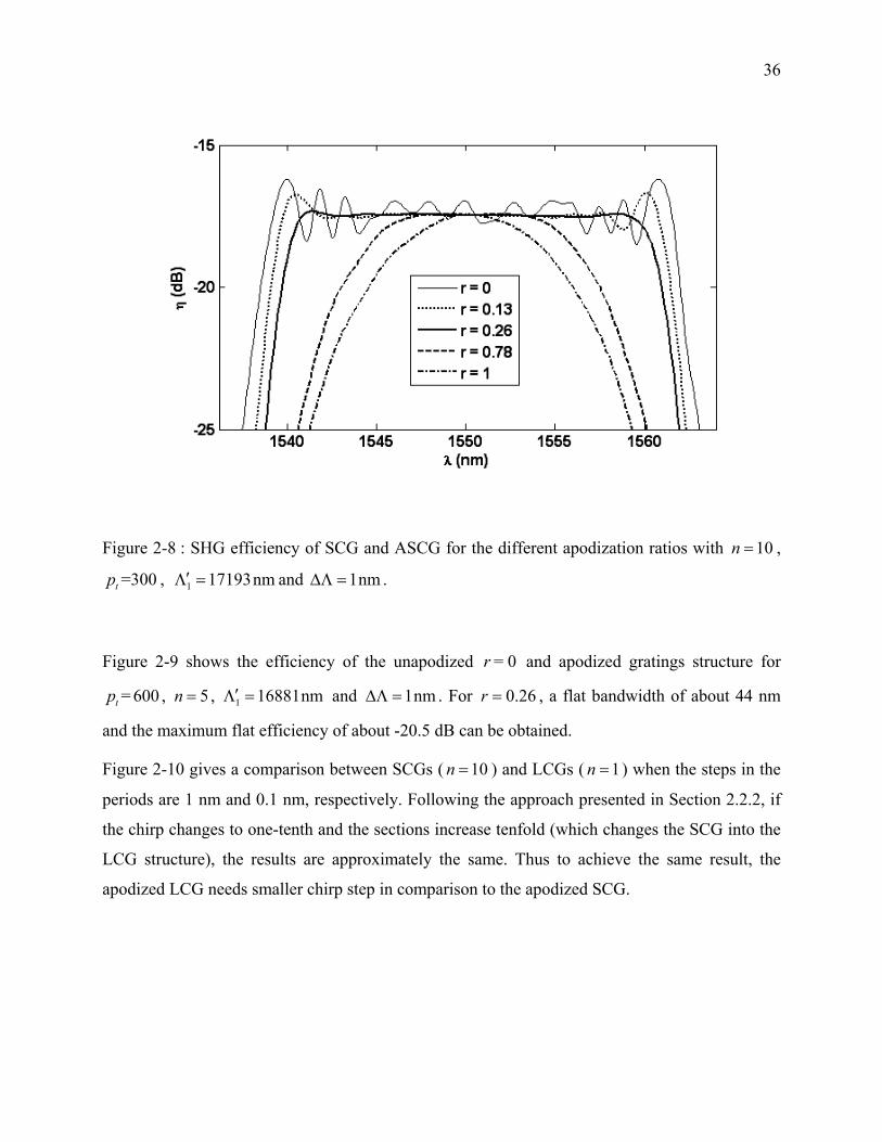
=300tp , 1 17193nm and 1nm . ...................................................................................... 36
Figure 2-9 : SHG efficiency of SCG and ASCG for the different apodization parameter with
5n , =600tp , 1 16881 mn and 1nm . ........................................................................... 37
Figure 2-10 : SHG efficiency comparison of ALCG and ASCG for the same length, with a high
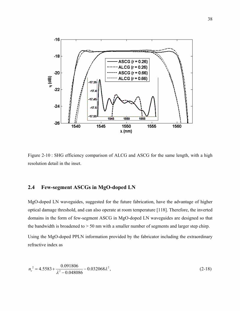
resolution detail in the inset. .......................................................................................................... 38
Figure 2-11 : SHG efficiency versus FH wavelength for 6-segment ASCGs with 0.40r and
different parameters. ....................................................................................................................... 40
Figure 2-12 : SHG efficiency versus FH wavelength with 0.40r for 5-, 6- and 7-segment
ASCGs when 50 mmtL . ............................................................................................................. 41
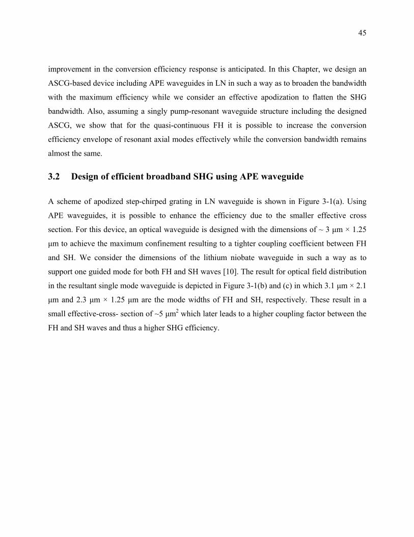
Figure 3-1 : (a) A Scheme of the proposed device. Optical field distribution for (b) FH (λω = 1550
nm) and (c) SH (λ2ω = 775 nm). ..................................................................................................... 46
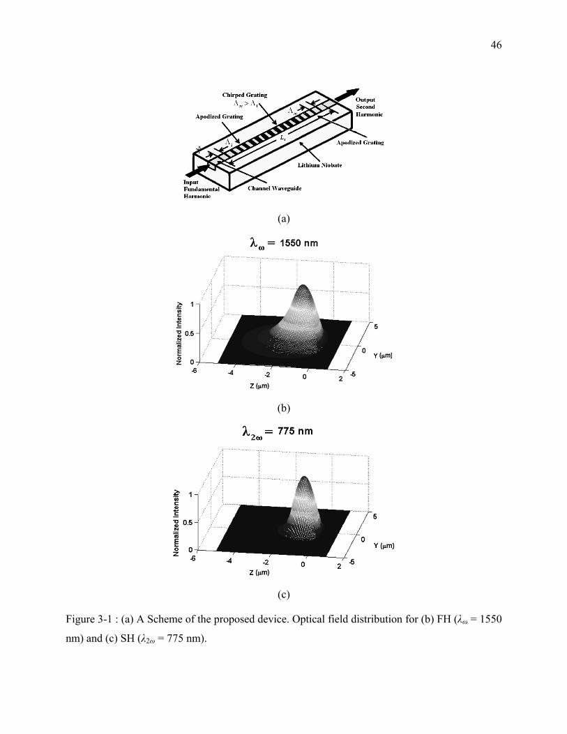
Figure 3-2 : Schematic of proposed ASCG structures (n > 1) with increasing and decreasing parts
of inverted domains. For n = 1, it converts to an ALCG structure. The up and down arrows refer
to the sign of χ(2) in white and black regions, respectively. ........................................................... 47
Figure 3-3 : SHG efficiency comparison of SCG and ASCGs for the different apodization ratios
where 10n and 0.75nm . .................................................................................................. 49
Figure 3-4 : SHG efficiency comparison of LCG and ALCGs for the different apodization ratios
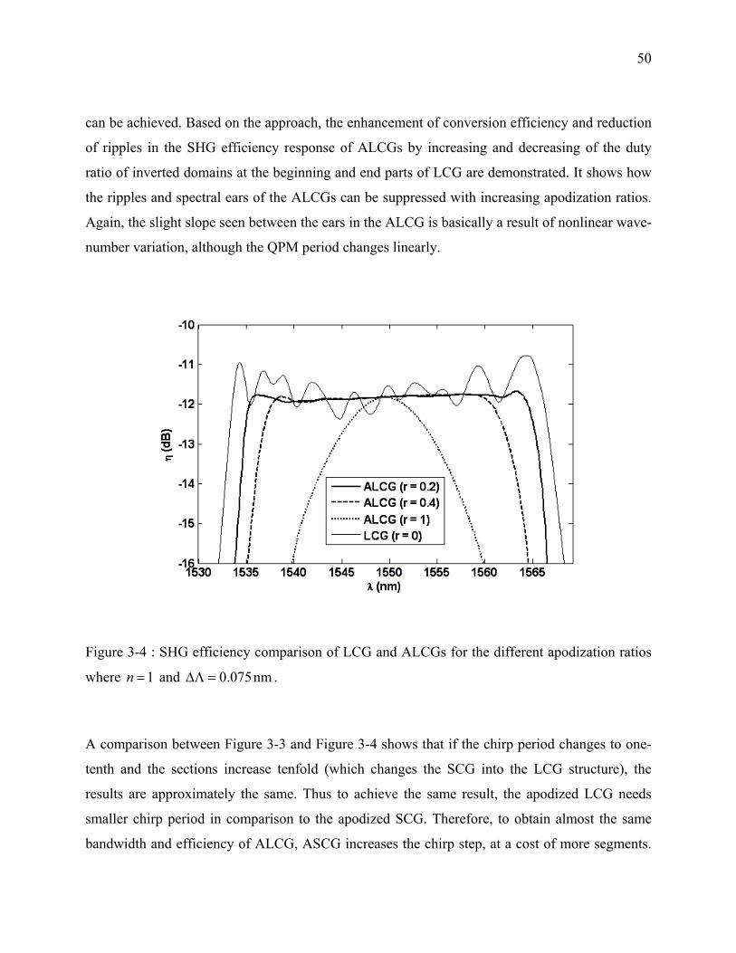
where 1n and 0.075nm . ................................................................................................... 50
Figure 3-5 : SHG efficiency comparison of LCG and SCG, and ALCG and ASCG for the same
length, with a high resolution detail in the inset. ........................................................................... 51
Figure 3-6 : Simple configuration of a singly pump-resonant waveguide for broadband ASCG-
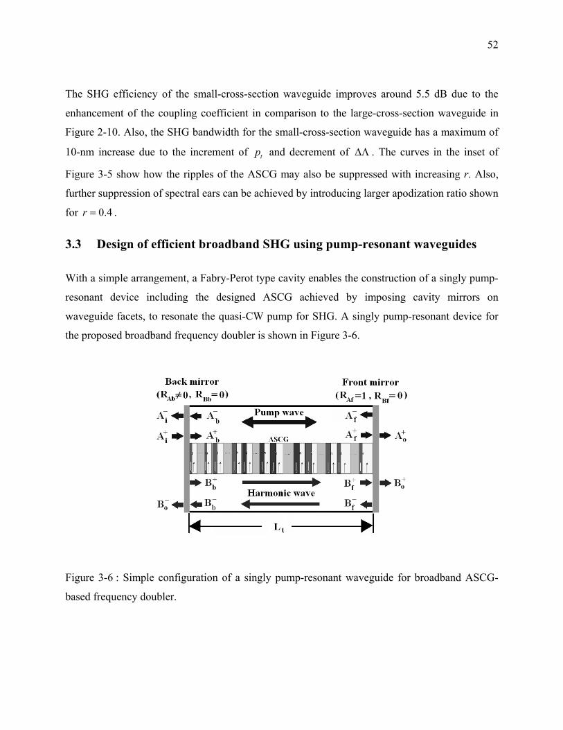
based frequency doubler. ................................................................................................................ 52
xxvii
Figure 3-7 : The envelope of SHG efficiency responses of the singly pump-resonant ASCG
versus FH wavelength, for 1AfR , 1dBtL and 5cmtL . .................................................... 54
Figure 3-8 : The envelope of SHG efficiency responses of the singly pump-resonant ASCG
versus FH wavelength, for 1AfR , 3dBtL and 5cmtL . .................................................... 55
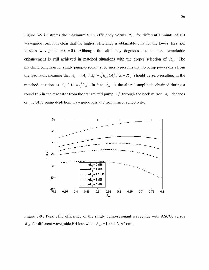
Figure 3-9 : Peak SHG efficiency of the singly pump-resonant waveguide with ASCG, versus
AbR for different waveguide FH loss when 1AfR and 5cmtL . .............................................. 56
Figure 3-10 : Peak SHG efficiency of the singly pump-resonant waveguide with ASCG, versus
input FH power for different waveguide loss and back-facet reflectivity when 1AfR and
5cmtL . ....................................................................................................................................... 58
Figure 4-1 : Schematic description of single-pass cascaded SFG + DFG scheme. ....................... 61
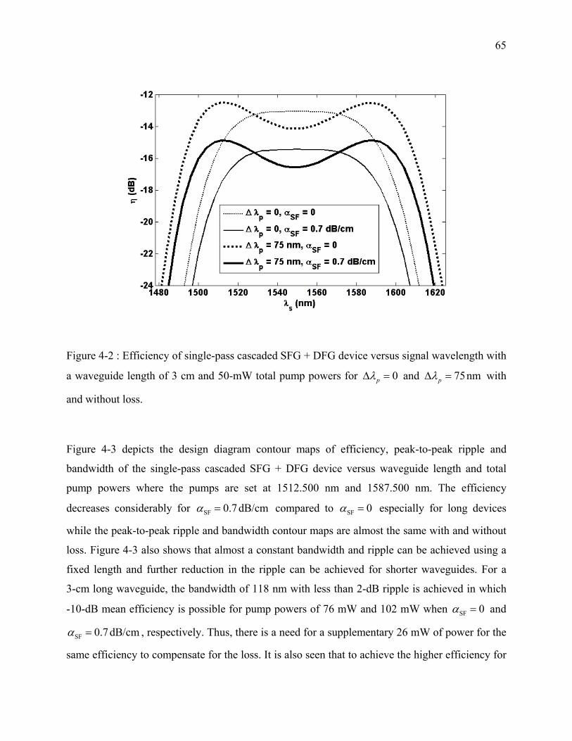
Figure 4-2 : Efficiency of single-pass cascaded SFG + DFG device versus signal wavelength with
a waveguide length of 3 cm and 50-mW total pump powers for 0p and 75nmp with
and without loss. ............................................................................................................................. 65
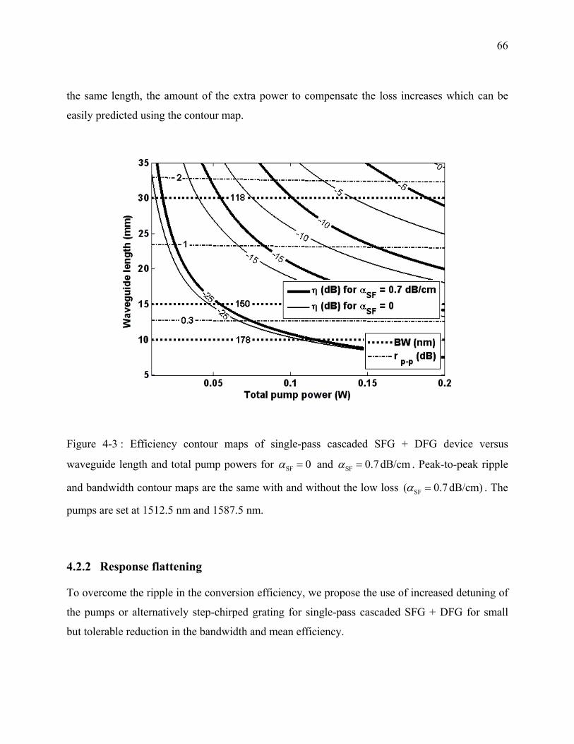
Figure 4-3 : Efficiency contour maps of single-pass cascaded SFG + DFG device versus
waveguide length and total pump powers for SF 0 and SF 0.7dB/cm . Peak-to-peak ripple
and bandwidth contour maps are the same with and without the low loss SF( 0.7dB/cm) . The
pumps are set at 1512.5 nm and 1587.5 nm. .................................................................................. 66
Figure 4-4 : Efficiency of single-pass cascaded SFG + DFG device versus signal wavelength for
3-cm lossless and low-loss waveguides when the pumps are set at 1512.5 nm and
21587.5 nm p and the total pump powers is 50 mW. .............................................................. 68
Figure 4-5 : Efficiency contour maps of the single-pass cascaded SFG + DFG versus waveguide
length and total pump power for SF 0 and SF 0.7dB/cm . Peak-to-peak ripple and
bandwidth contour maps are the same with and without the low loss SF( 0.7dB/cm) . The
pumps are set at 1512.5 nm and 1587.950 nm. .............................................................................. 69
xxviii
Figure 4-6 : Conversion efficiency of the single-pass cascaded SFG + DFG with uniform grating
versus signal wavelength for different period shifts when pumps are at 1512.5 and 1587.5 nm
(∆λp = 75 nm) and SF 0.7dB/cm . .............................................................................................. 71
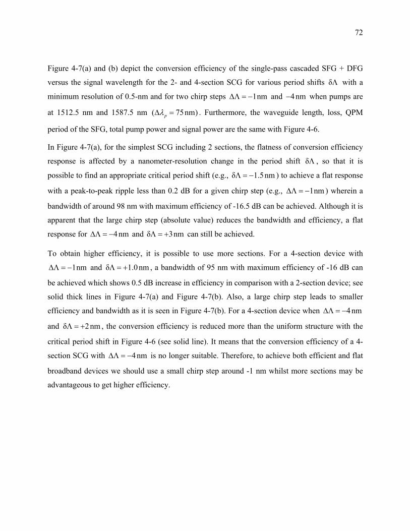
Figure 4-7 : Conversion efficiency of single-pass cascaded SFG + DFG versus signal wavelength
for (a) 2-section SCG and (b) 4-section SCG, for different period shifts and chirp steps when
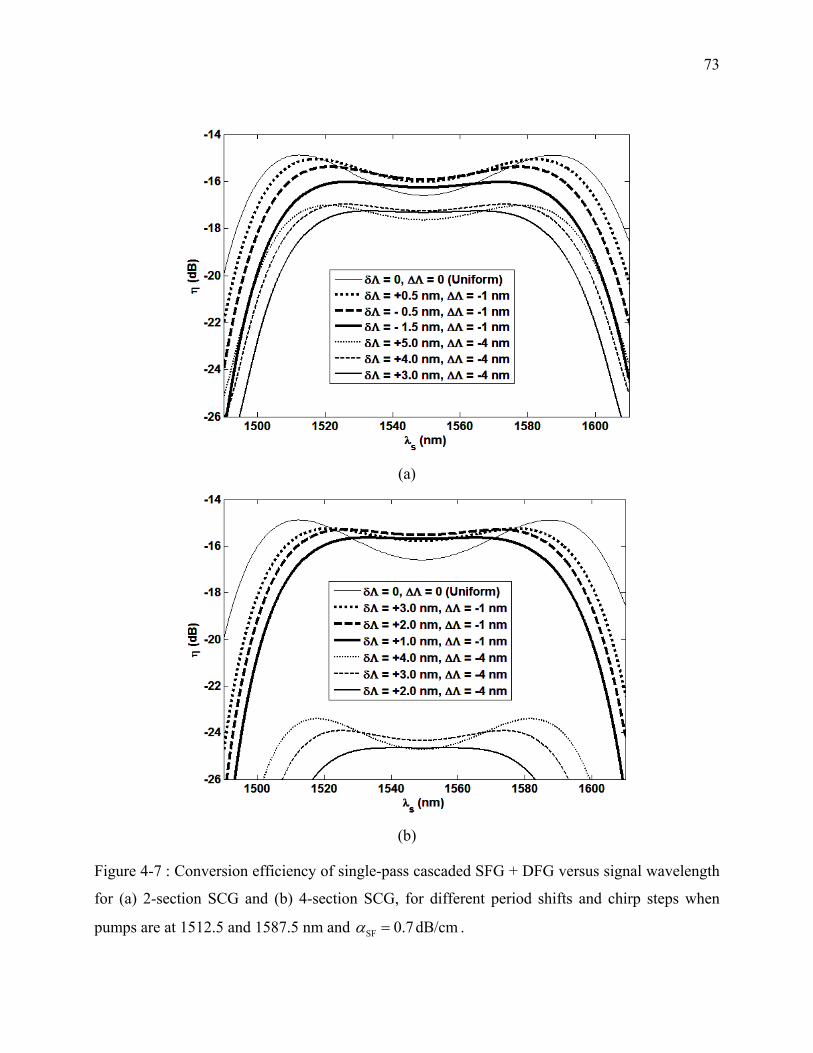
pumps are at 1512.5 and 1587.5 nm and SF 0.7dB/cm . ........................................................... 73
Figure 4-8 : Conversion efficiency of a 3-cm-long single-pass cascaded SFG + DFG versus signal
wavelength for 2- to 7-section SCG using -1-nm chirp step with their critical period shifts when
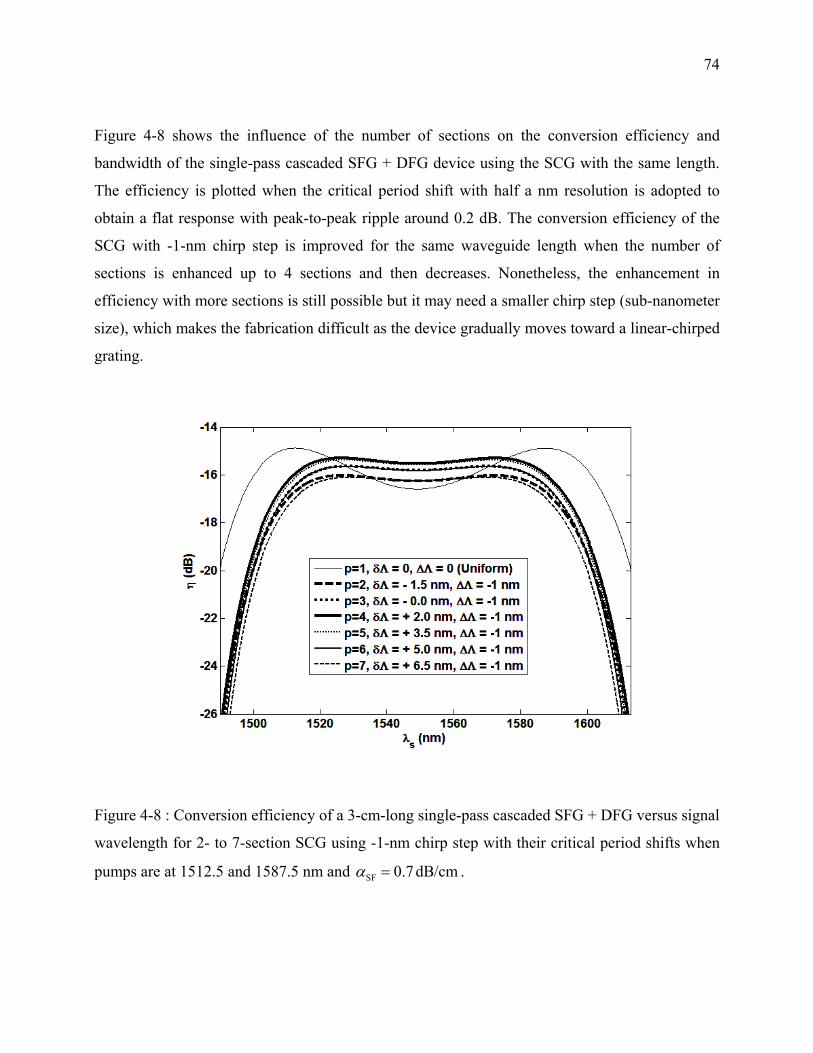
pumps are at 1512.5 and 1587.5 nm and SF 0.7dB/cm . ........................................................... 74
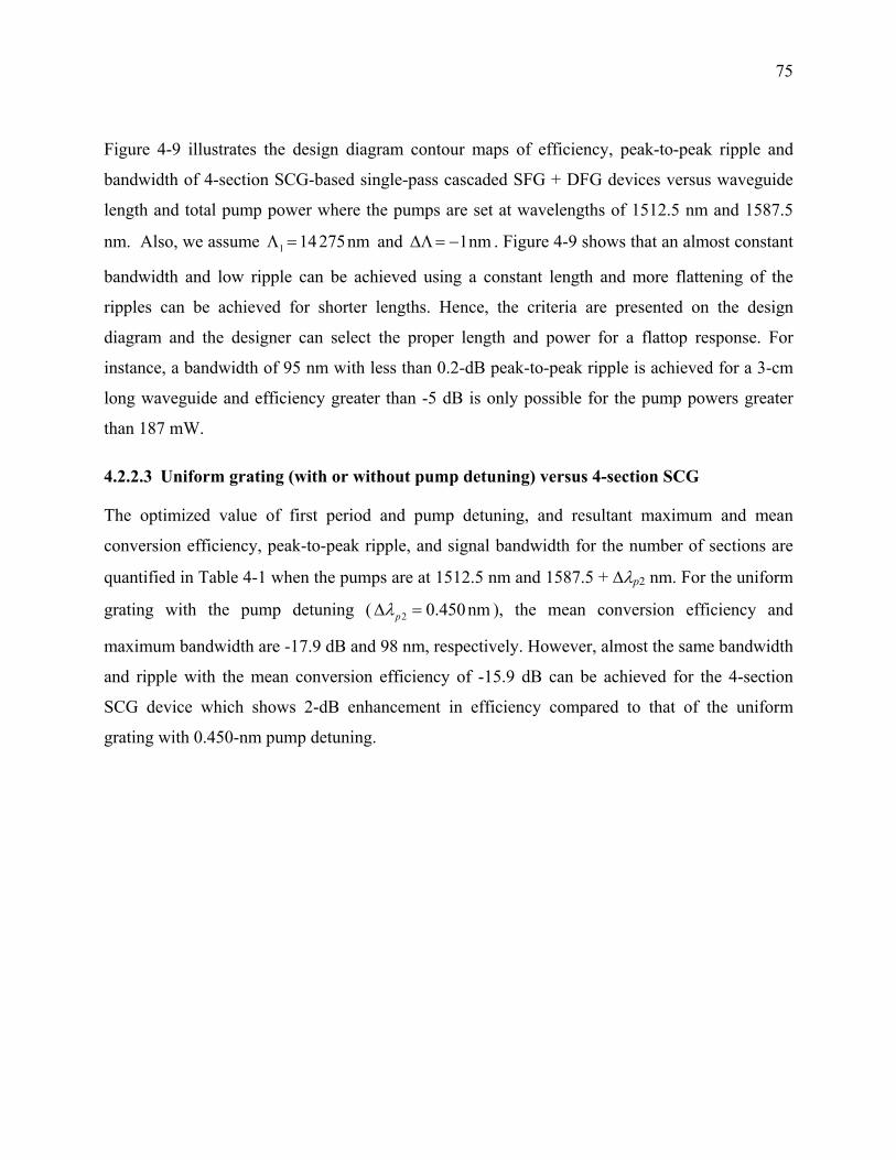
Figure 4-9 : Contour maps of conversion efficiency, bandwidth and ripple of the single-pass
cascaded SFG + DFG based device for a 4-section SCG with -1-nm chirp step and 2-nm critical
period shift when pumps are at 1512.5 and 1587.5 nm. ................................................................. 76
Figure 5-1 : Schematic description of the double-pass cascaded SFG + DFG. ............................. 79
Figure 5-2 : Efficiency of double-pass SFG + DFG device versus signal wavelength with a
waveguide length of 3 cm and 50-mW total pump powers for 0p and 75nmp with and
without loss. ................................................................................................................................... 82
Figure 5-3 : Contour maps of efficiency, peak-to-peak ripple and bandwidth of the cascaded
double-pass SFG + DFG device versus length and total power for the SF loss of 0.70 dB/cm
when the pumps are set at 1512.5 nm and 1587.5 + p2 nm for p2 = 0. ................................... 83
Figure 5-4 : Efficiency of double-pass cascaded SFG + DFG device versus signal wavelength for
a 3-cm long lossless and low-loss waveguides when the pumps are set at 1512.5 nm and
21587.5 nm p and the total power of the two pumps is 50 mW. ............................................ 85
Figure 5-5 : Contour maps of efficiency, peak-to-peak ripple and bandwidth of the cascaded
double-pass SFG + DFG device versus length and total power for the SF loss of 0.70 dB/cm
when the pumps are set at 1512.5 nm and 1587.5 + p2 nm for p2 = 0.225 nm. ...................... 86
xxix
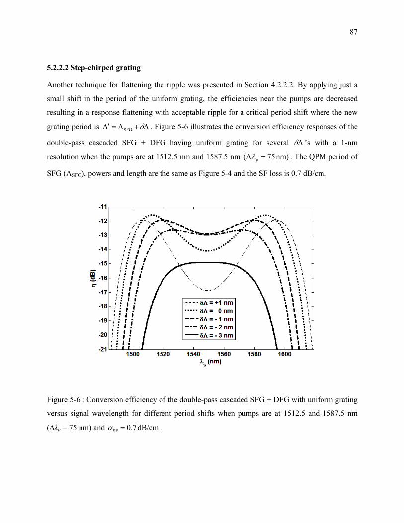
Figure 5-6 : Conversion efficiency of the double-pass cascaded SFG + DFG with uniform grating
versus signal wavelength for different period shifts when pumps are at 1512.5 and 1587.5 nm
(∆λp = 75 nm) and SF 0.7dB/cm . .............................................................................................. 87
Figure 5-7 : Conversion efficiency of a 3-cm-long double-pass cascaded SFG + DFG versus
signal wavelength for 2- to 5-section SCG with -1-nm chirp step with their critical period shifts
when pumps are at 1512.5 and 1587.5 nm and SF 0.7dB/cm . ................................................. 88
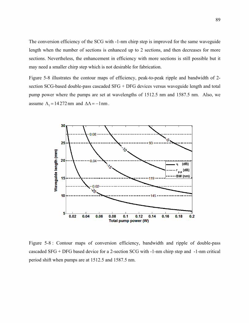
Figure 5-8 : Contour maps of conversion efficiency, bandwidth and ripple of double-pass
cascaded SFG + DFG based device for a 2-section SCG with -1-nm chirp step and -1-nm critical
period shift when pumps are at 1512.5 and 1587.5 nm. ................................................................. 89
Figure 5-9 : Conversion efficiency of wavelength detuned single-pass (p2 = 0.450 nm) and
double-pass (p2 = 0.225 nm) cascaded SFG + DFG based device versus signal wavelength for
different loss when the length and total pump power are (a) 2.5 cm and 100 mW and (b) 1.25 cm
and 400 mW. .................................................................................................................................. 93
Figure 5-10 : Conversion efficiency of 3-section SCG-based single-pass and double-pass
cascaded SFG + DFG versus signal wavelength for different loss when 1nm , 0 and
the length and total pump power are (a) 2.5 cm and 100 mW and (b) 1.25 cm and 400 mW. ...... 94
xxx
LIST OF ACRONYMS
ALCG Apodized Linearly Chirped Grating
APE Annealed Proton Exchange
aPPLN Aperiodically Poled Lithium Niobate
ASCG Apodized Step-Chirped Grating
BW Bandwidth
CW Continuous Wave
DFG Difference Frequency Generation
EDFA Erbium-Doped Fiber Amplifier
FH Fundamental Harmonic
FWHM Full-Width Half Maximum
LCG Linearly Chirped Grating
LN Lithium Niobate (LiNbO3)
MgO Magnesium Oxide
NLO Nonlinear Optic
OCT Optical Coherence Tomography
OTDM Optical Time Division Multiplexing
PPLN Periodically Poled Lithium Niobate
QPM Quasi Phase Matching
SCG Step-Chirped Grating
SFG Sum Frequency Generation
xxxi
SH Second Harmonic
SHG Second Harmonic Generation
THz Terahertz
Ti:LiNbO3 Titanium Indiffused Lithium Niobate (Ti:LN)
WDM Wavelength Division Multiplexing
WG Waveguide
xxxii
LIST OF SYMBOLS AND NOTATIONS
A Amplitude
a Duty ratio
a1Λ1 Minimum line width (inverted domain)
BW Device bandwidth
D Depth of waveguide
d Nonlinear coefficient
deff Effective nonlinear coefficient
E Electric field
j √-1
k Wavenumber
L' Input apodized grating length
L'' Output apodized grating length
L Unapodized grating length
Li Section (i) length (uniform grating)
Lt Total grating length
Lc Coherence length
n Number of segments
N Effective index at
n Refractive index at
p' Half number of apodized sections
xxxiii
p Number of unapodized sections
P Polarization
P0 Input power
pt Total number of sections
r Apodization ratio
R Reflectivity
rp-p Peak-to-peak ripple
Seff Effective Area
T Thickness of substrate
w Mode width
W Width of waveguide
α Propagation loss
β Propagation constant
δ Section bandwidth
Δ Total bandwidth
Δk Phase-mismatch parameter
Δn Refractive index difference
ΔΛ Chirp step
δν Linewidth (resonant frequencies)
Δν Mode spacing (resonant frequencies)
κ Coupling factor
Λ Period of inverted domain grating
τ Round trip time
xxxiv
τp Photon life time
Angular Frequency
Wavelength
c Central wavelength
0 Permittivity of free space
µ0 Permeability of free space
χ(i) Susceptibility of order (i)
1
CHAPTER 1
INTRODUCTION
1.1 Motivation
Nonlinear optics (NLO) has found many applications in photonics. This is in part due to the
availability of high quality nonlinear crystals such as lithium niobate (LN), and the access to the
largest nonlinear coefficients using domain inversion by periodic poling. This technique, known
as quasi phase-matching (QPM), ensures that the phases of the generated nonlinear waves remain
synchronized with the fundamental input wave by reversing the sign of the nonlinearity at a
period given by the dispersion of the material. There has been increasing interest in wavelength
converters based on QPM in waveguides because wavelength conversion can be done in different
wavelength bands within the transparency region of the medium by suitable design of domain-
inverted gratings. Nowadays, LN is the dominant ferroelectric material used in nonlinear
integrated optics. Built using periodically poled lithium niobate (PPLN) waveguides, quasi-phase
matched wavelength converters have attracted considerable attention because of their excellent
properties, having been extensively studied and found to have numerous applications in optical
communications, optical signal processing and optical sensing in the past decade. They are
intrinsically high speed, have a small size, high efficiency, low noise, high transparency to signal
modulation format amongst other advantages. There is also a need for broadband quasi-phase
matched wavelength converters in NLO waveguides, for ultrafast optical signal processing,
ultrashort pulse compression, variable and broadcast wavelength conversion in optical
communication, optical coherence tomography and displays. In this dissertation, new ideas for
realizing such wideband wavelength converters are addressed.
1.2 Second-order NLO wavelength conversion
When intense optical waves pass through a NLO crystal, the response of the crystal cannot be
considered linear [1]. The response generates optical waves at sum, difference and harmonic
2
frequencies. This mixing can be expressed using the relation between the dielectric polarization,
P, and the applied electric field, E
(1) (2) 2 (3) 30 ... , P E E E (1-1)
where ( )i is the i-order susceptibility tensor and 0 is the permittivity of free space. In Equation
(1-1) the space coordinates are implicit in the susceptibility. The applied electric field is the
driving term in the Maxwell’s equation generates the polarization. The first term in the right-hand
side of Equation (1-1) describes the first-order linear phenomena which are related to the phase
velocity causing refraction, reflection, diffraction and dispersion. The second term expresses the
first nonlinear response of the induced polarization, and is the second-order nonlinear effect,
absent in materials with inversion symmetry, such as glass but can be present in non-centro-
symmetric materials such as LN. The wavelength conversion in an NLO waveguide which is
covered in this dissertation is defined by this effect. The third term describes the third-order
nonlinear effects, present in all materials, and is responsible for effects such as self-phase
modulation, soliton formation, cross-phase modulation, four-wave mixing and so on which are
easily seen in optical fibers and have important implications in communications.
The most common second-order NLO effect used for wavelength conversion is second harmonic
generation (SHG). In this case, the frequency (ω) of the input optical wave or fundamental
harmonic (FH) is doubled to generate a second harmonic (SH) output wave if the condition is
satisfied amongst the relevant phase components. Further, the second-order χ(2) tensor of the NLO
crystal must include an appropriate component to couple a FH wave to a SH wave. It is common
to show the nonlinear coefficient d tensor instead of the χ(2) tensor. Considering SHG in LN
crystal, the Cartesian components of the polarization (2 )P are related to the components of the
applied electric fields ( )E by [2]
3
( ) 2
( ) 2
(2 )
( ) 231 22(2 )
0 22 22 31 ( ) ( )
(2 )31 31 33
( ) ( )
( ) ( )
( )
( )0 0 0 0
( )2 0 0 0 ,
20 0 0
2
2
x
y
x
z
y
y z
z
x z
x y
E
EP d d
EP d d d
E Ed d dP
E E
E E
(1-2)
where (2) / 2ml mld are the nonlinear coefficients which are expressed in a 3 × 6 matrix;
31 32 15 24 4.4pm/V d d d d , 22 21 16 2.4pm/V d d d and 33 25pm/V d .
The next second-order NLO wavelength conversion technique is difference frequency generation
(DFG), which is of great importance as it can cover the entire transparency range of NLO
crystals. The principle of operation is as follows: optical waves of two different frequencies are
mixed in these devices to generate the third optical wave with a frequency which is the difference
of the two input frequencies. Conversely, efficient generation of the sum-frequency occurs which
is called parametric up-conversion or sum frequency generation (SFG) if the condition is satisfied
amongst the relevant phase components.
1.3 Phase matching
SHG, DFG and SFG require phase matching to be efficient. For wavelength conversion, phase
matching is essential for building up the NLO response constructively [3]. This means that a
proper phase relationship between the interacting waves (for maximum wavelength conversion)
is maintained along the propagation direction, so that the amplitude contributions from different
locations to the resultant wave are all in phase. This leads to the condition that phase mismatch
has to be zero.
For example using SHG, there is a driving field at a frequency ω generating linear polarization at
ω and nonlinear polarization at 2ω. The phase-difference between the two oscillators (dipoles)
separated in the propagation direction is found by the product of the oscillator’s frequency and
the time which the driving field needs to travel between them. This time is equal to the ratio of
4
the propagation distance and the phase velocity of light in the material at the driving field
frequency. Therefore, the phase difference between the oscillators at ω is kωΔz, where kω = ωnω/c
is the wave-number of the FH, Δz is the distance between them, nω is the refractive index at ω
and c is the light speed. Similarly, the phase difference between the nonlinear oscillations at 2ω
is 2kωΔz. The SH field at 2ω generated by the nonlinear oscillator accumulates a phase of k2ωΔz
while traveling to get to the second oscillator where k2ω = 2ωn2ω/c is the wave-number of SH and
n2ω is the refractive index at 2ω.
If n2ω = nω is satisfied in a material, then the phase k2ωΔz just compensates the phase difference
of the nonlinear oscillations 2kωΔz and the fields at 2ω generated by the two oscillators interfere
constructively along the propagation direction resulting in growth of the SH power with
propagation distance. However, satisfying n2ω = nω presents a problem as common NLO
materials show normal dispersion, that is, n2ω > nω. Therefore, dispersion commonly causes a
non-zero phase mismatch (Δk = k2ω − 2kω ≠ 0) if no special measures are taken. To overcome this
difficulty two main approaches have been used: birefringent phase matching and quasi-phase
matching.
1.3.1 Birefringent phase matching
In NLO crystals, the refractive index depends on the polarization of the wave. This property can
be utilized to compensate the refractive index difference between FH and SH resulting from
normal dispersion. For example, considering SHG using uniaxial LN crystal, three orthogonal
axes exist as shown in Figure 1-1, denoted a, b, and c. The refractive indexes for the polarized
waves along the a and b axis are the same and called ordinary refractive index (no) whilst the
refractive indexes for the polarized wave along the c axis is smaller than no and called
extraordinary refractive index (ne). Therefore, the light propagating along the a-axis of LN travels
more slowly if it is linearly polarized along the b-axis than if it is linearly polarized along the c-
axis. If we restrict the polarization of the FH wave to be along the b-axis and the polarization of
the SH to be along the c-axis, the phase velocity difference due to dispersion can be compensated
for by the phase velocity difference due to birefringence, so that ne(2ω) = no(ω) and Δk = 0 which
results in the build-up of SH power as shown in Figure 1-2(a).
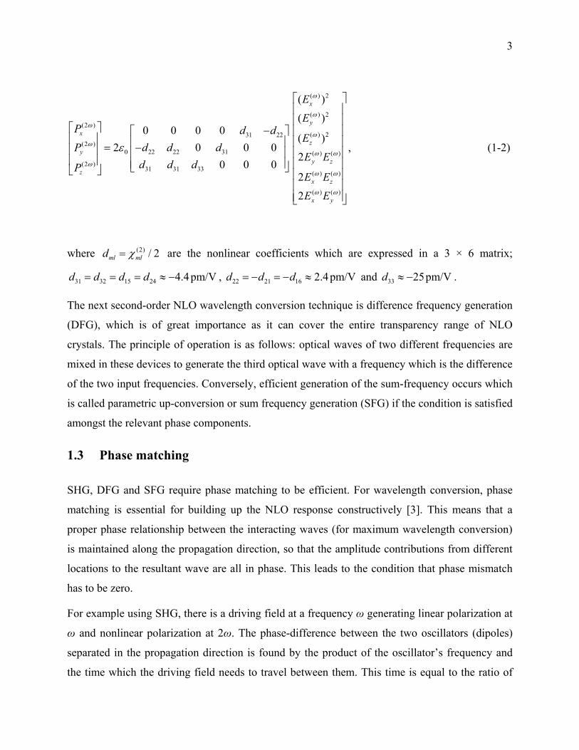
5
Although this configuration provides phase matching, it does not mean at once that it will
efficiently generate the SH as the nonlinear tensor must include an appropriate component to
couple a b-polarized FH to a c-polarized SH. An assessment of dml’s for the LN crystal in
Equation (1-2) exhibits that the required component is d31, which exists in LN. However, the
largest nonlinear coefficient d33 for LN is still not phase-matchable as we can not use the c-
polarized FH wave.
Figure 1-1 : A schematic view for using the LN crystal birefringence to obtain phase matching.
This technique may only work for a particular FH wavelength. For wavelengths below the FH
wavelength, dispersion of LN exceeds the birefringence and for wavelengths above the FH
wavelength, birefringence exceeds the dispersion. Nevertheless, as the involved refractive
indexes change differently with temperature, temperature tuning can be used to achieve phase
matching for some other wavelength. This is used to provide noncritical phase matching for the
desired wavelength. The term “noncritical” is often used as this technique is relatively insensitive
to the slight misalignment of beams. However, relatively high temperatures are required to obtain
phase matching for SHG in practice and these high temperatures may be a disadvantage in some
applications.
6
An alternative technique changes the direction of propagation rather than the temperature in order
to achieve phase matching. Phase matching for SHG may occur for some direction of propagation
in the a–c plane. In this arrangement, the SH is still polarized along the c-axis and experiences ne,
but the polarization of the FH in the a–c plane experiences the refractive index less than no and
phase matching may be satisfied for special wavelengths and angles of beam propagation.
However, this critical technique may also not be applicable to all wavelengths within the
transparency range of materials [2].
1.3.2 Quasi-phase matching
Using birefringent phase matching, the phase mismatch for SHG given by k2ω − 2kω becomes
zero and thus the condition n2ω = nω means that the FH at ω and the SH at 2ω travel through the
nonlinear crystal at the same speed as the index of refraction is a measure of the speed (phase
velocity). Phase matching ensures that SH contributions generated at each point along the crystal
add in phase, maximizing the total generated SH power. Otherwise, there is a phase mismatch of
k2ω − 2kω which leads to oscillations of the SH power as shown in Figure 1-2(b). In this case, the
maximum SH power is limited to the power generated over a small interaction distance,
Lc = π/(k2ω − 2kω) called coherence length at which the phase mismatch is equal to π. However,
the small coherence length is inadequate for efficient energy transfer to the SH component.
One solution to this problem was proposed in 1962 [4]. The technique, called quasi-phase
matching (QPM) is based on the resetting of the phase mismatch to zero at each coherence
length. After propagation in one Lc, the phase mismatch becomes π. If the sign of χ(2) is changed
at that position, an additional π phase shift is added to the nonlinear polarization, resetting the
phase mismatch to zero. Therefore, reversing the sign of χ(2) resets the mismatch to zero after a
length Lc. Thus, QPM permits the phase mismatch to be annulled over long lengths. In such way,
the power in the SH field is allowed to grow along the crystal, as shown in Figure 1-2(c).
7
Figure 1-2 : SH power versus crystal length for (a) phase matching and (b) no phase matching
and (c) quasi-phase matching schemes.
An important point here is that using birefringent phase matching in LN, it is not possible to
exploit the largest nonlinear susceptibility element (2)33 because it can be used only when all of
the interacting waves are polarized along the c-axis, whilst QPM is not subject to such constraints
because it depends on an externally imposed structure, rather than intrinsic dispersion properties
of the material. Thus, QPM can be used in order to take advantage of the highest nonlinear
coefficient in NLO materials.
QPM could not be realized at the time it was proposed as a concept, since appropriate fabrication
techniques had not been developed, and was first made in 1970 [5]. By the development of
advanced techniques for periodic poling to change the sign of χ(2), QPM in bulk crystals and
waveguides is widely used nowadays. QPM using periodic domain-inverted gratings in LN
waveguide, as shown schematically in Figure 1-3, is used extensively for SHG in order to
enhance the efficiency [6]-[7]. It offers several advantages such as phase matching at an arbitrary
wavelength by the use of d33, high conversion efficiency, and guided-mode harmonic output [8].
Nonetheless, most of the SHG-, DFG- and SFG-based devices use quasi-phase matched domain-
inverted gratings (periodically poled structures) and channel waveguides in LN.
8
1.4 Poling and waveguide fabrication in LN
For fabrication of quasi-phase matched gratings, the most popular technique uses liquid
electrodes and high-voltage pulse application [9]. In this method, a comb-shaped photo-resist
pattern (6-µm SiO2 layer) whose structure is the same as the poling period is formed on the
surface of an LN substrate with a thickness of ( 0.5mm)T using a conventional photo or
electron-beam lithographic technique. A liquid electrode consisting of saturated solution of
lithium chloride is applied to both sides of the LN surface while insulation between them is
preserved. The solution is confined within plastic frames sandwiching the crystal. A high-voltage
pulse (~coercive field 21kV/mm× = 10.5kVT ) is then applied to the LN substrate. This reverses
the spontaneous polarization under the electrode.
For fabrication of waveguides, titanium in-diffusion and annealed proton exchange (APE) in LN
are the most well known techniques [10]. Ti-diffused LN waveguides has been used in many
integrated optic devices. The diffusion source is a Ti film with thickness of 50-100 nm deposited
on the crystal surface. The source is thermally diffused into the crystal at ~1000ºC for several
hours. These waveguides with an index difference of ~0.01 support both the TE and TM modes
with very low propagation loss (as low as 0.1 dB/cm) at a wavelength of ~1.5 μm. However, APE
waveguides may be preferred because of their resistance to photorefractive damages and the
possibility of smaller mode fields due to tight confinement [11] but their losses are a little higher
at 0.35 dB/cm at a wavelength of ~1.5 μm. For APE waveguide fabrication, a mask pattern of
SiO2 is first formed photo-lithographically on the LN substrate. Proton-exchanged lithium
niobate optical waveguides are made by immersing the LN substrate at an elevated temperature
(160 - 240 ºC) into a proton donor solution such as benzoic acid for several tens of minutes. Parts
of the Li+ ions in the substrate are exchanged for protons to obtain a thin (several microns thick)
waveguide layer on the substrate. The proton-exchanged waveguides are thermally annealed
(~350 ºC) to diffuse protons from the initial layer to a deeper region of the substrate to anchor the
protons and stabilize the characteristics, reduce the relatively high propagation losses, and avoid
a reduction in effective nonlinearity. The resulting waveguide’s extraordinary refractive index is
higher than that of the substrate with a difference of ~0.09, while the waveguide’s ordinary
9
refractive index is lower than that of the substrate. Thus, the APE waveguides in z-cut LN (when
the cut of the crystal is perpendicular to c-axis) support only TM modes.
1.5 SHG, DFG and SFG in PPLN waveguide
The basic structure of a z-cut PPLN waveguide for SHG is shown in Figure 1-3. For frequency
doubling, the QPM condition for SHG is given by SHG 22 2π / and the period is
SHG c 22 ( / 2) / ( ) L N N where i , iN and i are the propagation constants, effective
indexes of guided waves and wavelengths of the FH and SH waves ( , 2 )i , respectively.
Moreover, an SHG bandwidth (BW) of a fraction of nm, inversely proportional to the length for a
few-centimeter long PPLN waveguide is achieved [11].
Figure 1-3 : A narrowband frequency doubler based on a uniform PPLN waveguide.
It is possible to utilize a PPLN waveguide for another second-order nonlinear mixing process
which is DFG as shown in Figure 1-4(a). When a signal wave of angular frequency s
(wavelength s ) and a pump wave of 02 p (wavelength 0 / 2p ) are mixed in a quasi-
phase matched device, a difference frequency (converted signal or idler) wave of c p s
(wavelength 1 1 1( )c p s ) is generated. The difference frequency c and the signal
frequency s are at points symmetrical to each other on the frequency axis with respect to the
10
half pump wave frequency, 0 . Thus, the DFG device can be considered a wavelength converter
from s to c . The QPM condition for DFG is given by DFG2π / s c p and the period
is 1
DFG / / /
p p s s c cN N N where i , iN and i are the propagation constants,
effective indexes of the guided waves and wavelengths of the signal and idler waves ( , )i s c and
pump frequency wave ( )i p , respectively.
Generally, DFG-based wavelength conversion has a large bandwidth, in which c is near to s
(waveband conversion), but it is difficult to couple both the pump and signal into the waveguide
as they are in different wavelength regions [11]. However, the use of cascaded χ(2) namely SHG +
DFG has been proposed to solve this problem. Consider a pump wave at 0 p and a signal
wave of s near to 0 coupled into the wavelength converter in which the QPM for SHG is
satisfied. The generated SH mixes with the signal wave to give rise to an idler wave at
2c p s when the QPM condition for DFG is satisfied. The configuration of the cascaded
SHG + DFG wavelength converter is shown in Figure 1-4(b). For wavelength conversion within
a communication band, an advantage of the cascaded SHG + DFG conversion is that the pump
wave is in the same band of the signal and idler waves. This allows use of fiber and
semiconductor lasers developed for optical communications instead of short wavelength lasers
for pumps.
The conversion efficiency of the cascaded SHG + DFG, however, is lower than that of ordinary
DFG for the same pump power. Although it is hard to obtain a high efficiency with a low-power
pump wave, an erbium-doped fiber amplifier (EDFA) can be used to increase efficiency. Further,
double-pass cascaded SHG + DFG has also been proposed to increase the conversion efficiency.
By means of the cascaded SHG + DFG, wide waveband conversion of optical signal is possible.
11
(a)
(b)
Figure 1-4 : (a) DFG scheme and (b) cascaded SHG + DFG scheme for broadband wavelength
conversion.
It is also feasible to use a PPLN waveguide to achieve SFG. With the two pump wavelengths, 1p
and 2p , the wavelengths of the sum frequency (SF) wave SF( ) is equal to 1 2 1 2/ ( )p p p p
provided that the QPM condition for SFG given by 1 2 SFG SF2π / p p is satisfied. The
QPM period for SFG thus is 1
SFG SF SF 1 1 2 2/ / /
p p p pN N N where i , iN and i are
the propagation constants, effective indexes of the guided waves and wavelengths of pumps
12
( 1,2)i and SF wave ( SF)i , respectively. SF 0 / 2 , where 0 is approximately the mean
wavelength of two pumps. By cascaded SFG + DFG, presenting advantageous feature including
wider bandwidth, waveband conversion of optical signal is also possible.
In the next two Sections, several applications for the broadband SHG and cascaded χ(2) are
discussed and novel solutions to reach such wavelength converters are presented.
1.6 Wavelength conversion using broadband SHG (frequency doubling)
Broadband frequency doublers based on quasi-phase matched SHG in waveguides have several
applications in optical communication and sensing [12]-[37]. Using broadband SHG, tunable
generation of coherent radiation at wavelengths where no appropriate laser is available, will also
be possible.
For optical communication, an important application of broadband SHG is in the variable and
broadcast wavelength conversion based on the cascaded SHG + DFG which needs a broadband
frequency doubler (SHG device) [15]. In earlier schemes, the pump bandwidth was narrow and
therefore signals could only be converted to limited wavelengths which restricted the usefulness
of the variable wavelength converter. Although, by imposing aperiodic quasi-phase matched
structures for SHG a large wavelength tuning range for the converter can be achieved using
multiple pumps, the pump wavelength channels are discrete and cannot be adjusted once the
aperiodic structures are fabricated [55],[56]. However, using broadband SHG by the
simultaneous use of Q pumps, R×Q wavelength broadcasting can be performed, in which each of
R input optical signals can be converted to Q output wavelengths [43]. Nonetheless, a bandwidth
more than 25 nm for broadband SHG is necessary to achieve a flexible broadcast wavelength
conversion [15].
Another example is in ultrafast optical signal processing [36], [37] in which the problem is
associated with generating ultrashort SH pulses in long quasi-phase-matched uniform gratings.
To minimize dispersive walk-off, the traditional technique uses a short piece of uniform grating
for large bandwidth but with only low efficiency. This works well when the input peak power is
large. When the grating length is too long to provide sufficient SH conversion efficiency, the
output SH pulses can be truncated and stretched in frequency and time domain, respectively due
13
to small conversion bandwidth. Nevertheless, the SHG of sub-picosecond pulses needs
broadband frequency doublers, e.g., a 26-nm bandwidth is enough to convert the pulses down to
∼100-fs duration [23].
Broadband SHG also seems promising in optical coherence tomography (OCT), a technique used
to diagnose various medical conditions [44]. In this case, a broadband SHG device acts as a new
broadband light source at shorter wavelengths. The reason for using the broadband source in an
OCT system is the inverse relationship between the bandwidth of light and axial resolution length
[45]. The use of the broadband light source in the near infrared is due to the fact that the axial
resolution length is also proportional to the square of light wavelength [45]. On the other hand,
for an OCT system a powerful light source is also required to achieve high detection sensitivity
for deep imaging in tissues [47]. However, an approach which is being suggested is to use
broadband frequency doublers to apply the broadband SH field simultaneously with the
broadband FH, namely dual-band OCT, and thereby benefit from differential OCT which may be
used to reveal otherwise unattainable data in one step [46].
Nonetheless, the problem associated with the PPLN-based frequency conversion is the
narrowband feature of SHG, as the bandwidth is dependent on the inverse of the grating length. A
simple solution is to use a short piece of PPLN waveguide to obtain wide bandwidth. To achieve
reasonable efficiency it needs very high input power which may not be tolerated by the PPLN
waveguide. Also, using an aperiodically poled lithium niobate (aPPLN), broadening (15 times) of
the phase matching bandwidth is achieved due to the scrambling of the phases compared to that
(0.3 nm) of a uniform grating with the same length [12]. However, the small bandwidth of the
non-flat SHG response is not suitable for the aforesaid applications. Although there has been
some work on waveguide structure to increase the bandwidth and tailored quasi-phase matched
grating structures have been proposed in the literature to broaden the phase matching, e.g., two
domain inverted building blocks and an aperiodic grating structure [26],[27], the bandwidths are
still a few nanometer. Thus, a high conversion bandwidth e.g., > 25 nm, with high efficiency
remains an unattainable goal. To solve this problem, the chirped grating scheme has been
proposed to broaden the bandwidth by chirping the pitch of the inverted domains as a function of
length [13]. Using this technique, broadening of the conversion bandwidth as a function of the
14
wavelength is achieved but with a fluctuated response, which is not acceptable for many
applications as the spectral conversion response is not uniform. Figure 1-5 shows a schematic of
the concepts of SHG bandwidth broadening in quasi-phase matched devices using a short
uniform grating and a long chirped grating of inverted domains.
In this dissertation, we propose a good candidate for the realization of a novel broadband
frequency doubler which is based on quasi-phase matched chirped gratings. In fact, the
engineering of gratings in quasi-phase matched devices seems promising to solve problems,
namely the broadband generation of SH optical wave with a desired spectrum and efficiency.
Figure 1-5 : Concepts of SHG bandwidth broadening in quasi-phase matched devices.
15
The potential of using chirped grating structures offers the advantage of obtaining larger
bandwidths. It is also important that they remain significantly more temperature tolerant than the
uniform gratings structures and provide a greater stability for frequency doubling. The potential
of using chirped grating structure for broadening the bandwidth in SHG has already been
theoretically analyzed [13]. However, there exist three problems using chirped gratings.
The first problem for realizing such broadband devices is the smallness of change in the linear-
chirped grating (LCG) period, which is typically around 100 picometers or less for a converter
with several nanometers of bandwidth. We will show for the first time that using the step-chirped
grating (SCG) enables us to increase the step size period change for more convenient fabrication,
while the bandwidth and efficiency remain almost the same in comparison to LCGs [38]. SCG
first introduced to broaden and flatten the reflectivity in fiber Bragg gratings [51].
The second problem is the obvious ripple on the efficiency curves of the LCGs and SCGs. One
method for flattening the SHG response is to use a grating structure with carefully located phase
shifts [25]. The other approach to solve this problem is to use apodization [52]. Here, we have
achieved this by changing the duty ratio of the poled regions, which removes the ripples and
achieves a nearly flat response [39].
The third problem is related to the mediocre SH efficiency using the ASCG. The efficiency may
be increased with small-effective-cross-section waveguides to increase the power density, with or
without resonant structures [40]. Thus, it is demonstrated for the first time that using singly
pump-resonant waveguides including ASCG, strong improvement in the SH conversion
efficiency response envelope curve is possible.
1.7 Waveband wavelength conversion using broadband cascaded χ(2)
During the past years, there has been considerable work in research and development of all-
optical wavelength conversion technology based on the cascaded χ(2) effects namely SHG + DFG
and SFG + DFG for future wavelength division multiplexing (WDM) systems in high-capacity
optical communications. For true flexibility, the 3-dB bandwidth of these converters should be
broad enough to cover the 1.55 µm optical window. For practical applications, it would be useful
if one can position the pumps at wavelengths out of the optical window, which is at least 75 nm
16
wide and should have flat responses and high conversion efficiencies. In addition to the
wavelength conversion function, these devices can perform different ultrafast optical signal
processing such as all-optical switching, offering possibilities of applications in ultrafast photonic
network systems based on optical time division multiplexing (OTDM) [41]. Cascaded χ(2)
wavelength converters also offer a variety of possibilities for applications in signal processing
including millimeter-wave/THz generation and radio over fiber.
For optical communications, the most notable advantage of cascaded χ(2) devices is the extremely
wide wavelength coverage while the pump(s) and signal/idler are in the same band. The
converters based on cascaded χ(2) in PPLN waveguides are superior to others [42], as they can
offer a high efficiency with a moderate pump power and can simultaneously convert a batch of
broadband wavelengths or high-speed signals, with negligible signal-to-noise ratio (SNR)
degradation. Another advantage as coherent wavelength converters, is full transparency to
various signal formats. They can also perform bidirectional wavelength conversion.
Compactness, compared to fiber devices and integration compatibility are among the other
advantages of these devices.
DFG [75]-[81] and cascaded SHG + DFG in PPLN waveguides, has already been demonstrated
both theoretically and experimentally as a wavelength conversion scheme in several applications
[82]-[93]. For wavelength conversion within a communication band, an advantage of the single-
pass cascaded SHG + DFG to DFG is that a pump wave with the wavelength in the same band of
the signal and idler waves can be used. However, it is hard to obtain high efficiency with a low
pump power in the single-pass cascaded SHG + DFG scheme. To solve this problem, the double-
pass cascaded SHG + DFG is a good technique to increase the efficiency in comparison to that of
the single-pass one but has a small bandwidth penalty [82],[83]. Nevertheless, the disadvantage
of both SHG + DFG schemes e.g., for WDM systems is that several channels must be sacrificed
because the wavelength of the pump light must be set at the centre of the conversion band
occupying the place of possible channels. Furthermore, highly broadband SHG + DFG need
gratings with complex structures, periodically distributed π-phase shifted domains or chirped
optical superlattices [78],[79],[80].
17
Recently, an interesting wavelength conversion technique based on quasi-phase matched
cascaded SFG + DFG has been demonstrated theoretically and practically in PPLN waveguides
and found wide applications including broadband wavelength conversion, channel selective and
multiple channel wavelength conversion, and format conversion [94]-[113]. By increasing the
pump wavelength difference using this technique, the bandwidth can be enhanced [98]. However,
the mean of the conversion efficiency depends on the wavelengths of the pumps and is decreased
by increasing the pump wavelength difference. To overcome the efficiency reduction, a double-
pass cascaded SFG + DFG scheme has been proposed, which is also able to filter out the residual
pump wavelengths at the output [109]. Nonetheless, for wide pump wavelength difference, SFG
is perfectly phase-matched whilst the DFG phase-mismatch is large when the signal is far from
the pump wavelengths. Thus, the wide pump wavelength difference increases the variation of
conversion efficiency, converting equal-power signal channels unevenly [115].
Although the cascaded SFG + DFG schemes have been principally investigated, the research on
how to set the pumps exactly or alternatively to engineer the grating to improve the conversion
properties still remain and are of great importance [114]. Solutions to the problem are proposed
for the first time, in single-pass and double-pass devices using detuning of the pump wavelength
[116], [117], or alternatively using step-chirped gratings. We show that, if the wavelength of a
pump or the chirp step in the SCG is increased slightly, the SFG phase-mismatch decreases and
the DFG phase-mismatch is also reduced, which leads to flattening of the variation in the
response curve.
1.8 Overview of the dissertation
In Chapter 2, the engineering of quasi-phase matched chirped gratings including inverted
domains for SHG in low-loss titanium in-diffused lithium niobate (Ti:LN) waveguides is
presented in such a way as to broaden the bandwidth significantly. A design formula is proposed
for the first time to help decide how many segments are needed as a design rule, dependent on the
required bandwidth. In addition, we consider an apodization method to flatten the SH bandwidth
by utilizing increasing and decreasing patterns of inverted domains into the quasi-phase matched
gratings. More generally, the proposed concept of apodized step-chirped grating (ASCG) may be
18
applied to broadband QPM in other NLO materials, with or without a waveguide. Finally, the SH
conversion bandwidth of > 50 nm may be designed with a special design of few-segment ASCG
in LN with a 1-µm line width in such a way as to provide a flat response and also facilitate the
poling and fabrication processes.
In Chapter 3, it is shown that the moderate SHG efficiency of the ASCG in Ti:LN waveguides
can be boosted using small-effective-cross-section waveguides. To achieve this goal, APE
waveguides are considered because of the possibility of higher index difference and smaller mode
field cross section. Also, assuming a singly pump-resonant waveguide for broadband SHG using
the ASCG, it is demonstrated that for the quasi-continuous FH it is possible to increase the
conversion efficiency envelope of resonant axial modes effectively while the conversion
bandwidth remains almost unchanged. Furthermore, it is shown numerically for an ASCG that by
means of singly pump-resonant waveguides, the conversion efficiency of quasi-continuous waves
shown with the envelope of responses increases substantially, especially for low propagation loss.
The optimized values of back-facet reflectivity and input power to achieve the maximum
efficiency, for several waveguide loss parameters are also presented.
In Chapter 4, we evaluate and compare numerically the properties of the single-pass cascaded
SFG + DFG and SHG + DFG schemes when the pump wavelength difference is 75 nm and 0 nm,
respectively and show that for the same device length, the adoption of the SFG + DFG device
further improves the bandwidth performance with a small efficiency reduction and a slight ripple
penalty. Moreover, we present the criteria for selection of the waveguide length and pump
powers to obtain the required efficiency, ripple and bandwidth and show that increased
wavelength detuning of a pump in the single-pass device, removes the ripple with a penalty on
the mean efficiency. Further, introducing a few-section SCG device with the proper design,
results in almost the same bandwidth and flatness, with less mean efficiency penalty compared to
the counterpart pump-detuned device. Additionally, we present design diagrams for pump-
detuned and SCG single-pass devices for selection of the length and pump powers to obtain the
required efficiency, ripple and bandwidth.
In Chapter 5, the properties of the double-pass cascaded SFG + DFG and SHG + DFG schemes
are evaluated and compared numerically when the pump wavelength difference is 75 nm and
19
0 nm, respectively. It is demonstrated that for the same device length, the adoption of the double-
pass SFG + DFG in a low-loss waveguide device, with pump detuning or using a SCG, further
improves the conversion efficiency with a small bandwidth reduction compared to the single-pass
SFG + DFG device. Further, it is shown that for the same length and power, the efficiency
enhancement advantage, expected due to the use of the double-pass device instead of the single-
pass one, is lost when the waveguide loss reaches a particular value. Moreover, we present the
design diagrams of pump-detuned and SCG double-pass devices for choice of the length and
pump powers to obtain the necessary efficiency, ripple and bandwidth.
In Chapter 6, we conclude the work and propose some new ideas for future work.
20
CHAPTER 2
BANDWIDTH BROADENING AND FLATENNING
OF QUASI-PHASE MATCHED SHG USING
APODIZED STEP-CHIRPED GRATING
2.1 Overview
An important requirement for exploiting the second-order nonlinearity for harmonic generation
and frequency conversion is phase matching to accumulate NLO response constructively. We
have seen in the last Chapter that the QPM structure presents us with significant advantages.
Nevertheless, the QPM bandwidth broadening for SHG has attracted considerable attention [12]-
[37]. Modified quasi-phase matched structures have been proposed to broaden the phase
matching and the segmented gratings have also been demonstrated for the SHG bandwidth
broadening, however, the bandwidth was only broadened to 1.12 nm [21]. Although, there still
exists a need for higher conversion bandwidth, e.g., more than 25 nm with flat conversion
response, highly-broadband SHG in quasi-phase matched waveguides have not been achieved
successfully.
The capability of using chirped grating structure, offers the benefit of obtaining large SHG
bandwidth [13]. However, there exist three problems using chirped gratings for broadband
frequency doubling. The first problem is the smallness of change in the linear-chirped grating
(LCG) period. We show that a step-chirped grating (SCG) structure can solve the problem. Using
SCG enables us to increase the period change for the convenience of fabrication while the
bandwidth and efficiency remain almost the same in comparison to LCG. The second problem is
the noticeable fluctuations on the broadband SH efficiency responses of chirped gratings. Our
approach to solve this problem is the imposing of some apodization [52]. It can be done by
changing the duty ratio of the poled regions in chirped gratings which helps to remove the ripples
21
and achieve flat responses. The third problem is related to conversion efficiency which will be
addressed in Chapter 3.
In this Chapter, we propose the engineering of SCG in such a way to highly broaden the
bandwidth with large chirp steps. A formula is proposed to decide how many segments one
should use as a design rule dependent on the required bandwidth. Also, we consider an effective
method to apodize and nearly flatten the SH bandwidth by considering increasing and decreasing
patterns of inverted domains into the quasi-phase matched gratings, in low-loss lithium niobate
waveguides with propagation loss around 0.1 dB/cm, e.g., Ti:LN [23], [34], [90], [101].
However, the proposed concept of apodized step-chirped grating can be applied to other kind of
NLO materials and waveguides.
2.2 Modeling of step-chirped grating
For the frequency doublers based on SHG taking advantage of QPM, any phase mismatch
between laser wavelength and gratings should be resolved. Uncertainty in the propagation
constant, error in the fabrication process and fluctuation of the laser wavelength and temperature
variations may increase the mismatch. Not only does a SCG provide a better means for
fabrication of highly-broadband converters but also is able to solve the above problems by
broadening the phase matching bandwidth.
A SCG structure is proposed as shown in Figure 2-1. In this structure, the total grating length (L)
has been divided into p sections that each section consists of n constant periods i or n segments
as a uniform grating with a 50% duty factor which is the ratio of the domain-inverted region to
the period. Therefore, the section length is ( , 1, 2, ..., )i iL n i p . The period of the sections
changes according to a function which we assume to be
1 ( 1) ,i i (2-1)
22
Figure 2-1 : Scheme of a domain-inverted SCG. The plus and minus signs refer to the sign of χ(2)
in gray and white regions, respectively.
where 1 is the period of the first section, is the chirp step or period change between two
adjacent section. To obtain the total SH wave amplitude and efficiency, we can consider p
uniform gratings in PPLN. The calculations begin and cascade from the first section with the
length 1L to the last section with the length pL , in which we use the nonlinear coupled mode
equations [13]
Δ 12( ) ( ) ( ) ( ),j kx
FH FH SH FH FH
dA x j A x A x e A x
dx (2-2)
2 Δ 12( ) ( ) ( ),j kx
SH FH SH SH
dA x j A x e A x
dx (2-3)
to describe SHG in each section which are solved numerically to take into account pump
depletion. ( , )FH FHA and ( , )SH SHA are the amplitudes and losses of the FH and the SH waves,
respectively and Δk is the phase mismatch parameter of each section defined as
23
2Δ 2 2π / ik where 2π / N and 2 2 22π / N are the mode propagation
constants of the FH and SH waves, respectively. Moreover, ( , ) N and 2 2( , ) N are the
effective refractive indexes and wavelengths for the FH and SH waves, respectively. Also, the
coupling factor can be shown as [11]
3/2 220
0 22 0
(2 ),
2( )
eff
eff
d
N N S (2-4)
where 0 is the permeability of free space, 33(2 / π)effd d is the effective nonlinear coefficient
for 50% duty ratio and the effective area is [11]
22 2
2
22
2
( , ) ( , ).
( , ) ( , )
eff
E y z dydz E y z dydzS
E y z E y z dydz (2-5)
where ( , )E y z and 2 ( , )E y z are the normalized mode profiles for the FH and SH waves,
respectively in a z-cut LN waveguide, which is assumed to have a uniform cross section and to be
parallel to the optical axis a which is called here the x-axis. Equation (2-4) shows that the
coupling factor is directly proportional to the effective nonlinear coefficient and inversely to the
square root of the effective area. The effective area of a ~6 μm × 3 μm LN waveguide with the
maximum index difference of 0.01 is 220μm .
The phase mismatch parameter Δk of each section is calculated first by finding the extraordinary
indexes for different wavelengths using the Sellmeier expression in LN
24
82 2 7
2 8 2
0.0992 5.2716 104.5820 0.021940 2.2971 10 ,
(0.21090 4.9143 10 )
e
Fn F
F (2-6)
where λ is the wavelength in µm and F = 894.75 at 26º C [11]; and second by applying the
effective refractive indexes of the waveguide [10]. Finally, the SHG conversion efficiency is
defined as
2 2( ) / ( 0)SH FHA x L A x . (2-7)
2.2.1 Bandwidth of a section in a step-chirped grating
We can now obtain an approximate expression for the bandwidth of a section in an SCG. We
choose the length 1L of the uniform grating consisting of n segments of period 1 . For the loss-
less case that the pump is also non-depleting, the efficiency is given as 22 20 1 sin /P L u u where
1Δu kL and 20 (0)FHP A is the incident FH power. Neglecting the wavelength dependence of
, the FWHM bandwidth of a section is attained (see later) when the efficiency drops to 0.5
where 1Δ 1.39u kL , then
11
21.39,N L
(2-8)
where / 2c and 2N N N . For c , we have
25
22
,2
c c c
N N NN (2-9)
where we assumed ( ) ( )cN N . Substituting Equation (2-9) in (2-8), we obtain
1
1 1
1.39 2.78 0.88.
π πc
c N L L n
(2-10)
Therefore, the bandwidth of a section in an SCG is approximately equal to the product of the
central wavelength and the ratio of the period of the grating to the total length of the section. In
other words, the bandwidth of a section decreases as the number of the segments increase, thus
the SCG bandwidth will be smaller. Equation (2-10) is a basic rule for the bandwidth calculation
of a section in a SCG structure. For example, using a 10-segment SCG device ( 10)n , a rough
estimate of maximum bandwidth for each section is approximately calculated using Equation
(2-10) as 0.88 / 135nmc n near 1550 nm. In the next Section, it will be studied how the
SCG bandwidth varies with the change of the SCG fundamental parameters of p, n and .
2.2.2 Design considerations of step-chirped grating
To understand how the SCG bandwidth changes for the different SCG fundamental parameters of
p, n and , several combinations are simulated. Figure 2-2 to Figure 2-5 show the efficiency of
the SCG versus the FH wavelength for different p, n and parameters. Also, the FH input
power is assumed 50 mW. Considering a 50-nm bandwidth around 1550 nm requires the grating
length of ~10 cm where the period of SCG starts as 1 16881nm and therefore 6000 n p is
achieved. Thus, for 10n , 600 sections exist and the chirp step around 1 nm is necessary to
cover the 3-dB bandwidth of 50 nm which is shown in Figure 2-2. It is seen that for broadband
SHG, interference among phase matching conditions causes large ripples on the conversion
efficiency response with the peak-to-peak of around 3 dB.
26
Figure 2-2 : SHG efficiency of SCG versus FH wavelength for different number of sections p,
10n and 1nm .
However, a shorter length results in a smaller bandwidth and a bandwidth of 25 nm for the SCG
is achieved with about 300 sections where the average efficiency over the bandwidth is about
-17.5 dB whilst using the uniform grating with the same length of ~5 cm, the bandwidth less than
half a nanometer and the efficiency near 0 dB can be achieved.
In Figure 2-2, the SCG structure needs a total length more than 5 cm for the bandwidth greater
than 25 nm which is hard to fabricate on LN substrates. To attain the bandwidth of 50 nm with a
< 5-cm-long SCG, one possibility is to decrease n. In other words, at the expense of losing
efficiency we reach the same bandwidth with the shorter SCG which is suitable for fabrication.
This case for 5n is depicted in Figure 2-3. Actually, the conversion efficiency of the new SCG
is almost 3-dB lower than that of Figure 2-2 because of the length of each section has been
decreased to half.
27
Figure 2-3 : SHG efficiency of SCG versus FH wavelength for different number of sections p,
5n and 1nm .
Another possibility to achieve the maximum bandwidth of 50 nm with a shorter SCG length, is to
increase the chirp step. Figure 2-4 illustrates the efficiency for 10n and 2nm . It is
obvious that the efficiency drops by almost 3 dB when the chirp step is doubled, with increased
fluctuation on the efficiency response in comparison with Figure 2-2. Also the average efficiency
is more slanted as a function of wavelength. So, there is an upper limit for increasing the period
as it leads to a sloping response with wavelength and reduces the bandwidth.
Noteworthy conclusion results from the comparison of Figure 2-3 and Figure 2-4 with Figure
2-2, which is useful for understanding the importance of the SCG structure. For a constant length,
doubling the sections (e.g. halving the segments), nearly doubles the bandwidth and halves the
efficiency. On the other hand, doubling the chirp step , also roughly doubles the bandwidth
and halves the efficiency.
28
Figure 2-4 : SHG efficiency of SCG versus FH wavelength for different number of sections p,
10n and 2nm .
Figure 2-5 shows the efficiency for 5n and 0.5nm . The result is almost the same as
Figure 2-2. Consequently, doubling the sections and halving the chirp in Figure 2-2 gives
approximately the same result as seen in Figure 2-5. Following the same approach, if the chirp
changes to one-tenth and the sections tenfold (segments changes to one-tenth), the result remains
approximately as Figure 2-2. So, to achieve the same result, the LCG structure needs a smaller
period difference in comparison to the SCG structure. Then, to achieve almost the same
bandwidth and efficiency, instead of a smooth linear chirp, using a step chirp increases the
difference in periods which is convenient for fabrication.
29
Figure 2-5 : SHG efficiency of SCG versus FH wavelength for different number of sections p,
5n and 0.5nm .
By examining the results of the previous SCG structures, it appears that for 1nm , the
number of sections required for an acceptable unit bandwidth in nm from the grating is also a
constant, i.e. 12 sections. To study the significance of the chirp step, we note that the
approximate FWHM bandwidth of a section with period is given by Equation (2-10) and
noting the total bandwidth and length L in meters and 12 / ,p we get the bandwidth
of the section which is equal to 10 / ( )c L . Thus, using the total length of around 5
cm, the central frequency at 1550 nm and the chirp step of 1 nm, the bandwidth of each section is
related to the SCG bandwidth by
5.4 . (2-11)
30
The interesting conclusion is that for the constant length of 5 cm, the bandwidth of each section
of the SCG should be greater 5.4 times the total bandwidth. If we need to design a 50-nm-
bandwidth SCG with the length of around 5 cm and 1nm , according to Figure 2-1,
/2/ pn L p and the SCG will be realized with the number of segments equal or less than 5 (see
Figure 2-3).
Additionally, fewer sections in the same length of the SCG give better efficiency because they
have more segments. By examining Figure 2-2 and Figure 2-3 we understand that the 50-nm
bandwidth can be achieved in both (600 sections: 10 segments) and (600 sections: 5 segments)
schemes, but in the latter the length and the average efficiency are almost halved.
2.3 Apodized chirped gratings
In the preceding Section, it was found that the chirped grating enables us to broaden at will the
phase matching bandwidth of SHG. However, the technique results in some non-uniformity in
the broadband conversion efficiency response of frequency doublers. The ripple feature of SCGs
in Figure 2-2 to Figure 2-5 is created by the interference among the constituent phase matching
spectra originating from different positions in the gratings. In the following, we consider it more
precisely how to remove those noticeable ripples.
The wave equation governs the electric field ( , )E x t propagation in the presence of nonlinear
polarization ( , )NLP x t in the nonlinear medium where the polarization is only a perturbation to the
system. Assuming that both the electric field and nonlinear polarization are scalar plane waves
and invoking the slowly varying envelope approximation, it can be described as follows [1]
2 2 2
0 02 2 2( , ) ( , ) ( , ).
NLE x t E x t P x tx t t
(2-12)
The wave equation is derived in the frequency domain by taking the Fourier transform of Eq.
(2-12) given by
31
22 2
0 02( , ) ( , ) ( , ).
NLE x E x P x
x (2-13)
Describing the fields in complex notation as ( ) ( )12( , ) ( , ) ( , ) , jk x jk xE x x e x eE E and
assuming the slowly varying envelope approximation, Equation (2-13) can be simplified
approximately as
( )0
( )
( , ) ( , ) .2
jk x
NL
cx j x e
x nE P (2-14)
It is possible to define the spectrum of nonlinear polarization leading to SH field with the relation
,2 0( , ) ( ) ( ) jkx jkxNL effx d e eP E E (2-15)
where stands for convolution. Thus, Equation (2-14) gives the equation governing the SH
field as
( , )2 0
( , ) ( ) ( ) ,
j k x
effx j d e dxE E E (2-16)
where 0 2/ n c and ( , ) ( ) ( ) ( )k k k k which is a function of the
frequencies at the SH ( ) and FH ( ) . By integrating Equation (2-16) over the total length, the
SH spectrum at the output of the converter of length L is
32
( )2 ( , ) ( ) ( ) j k x
t effover LL j d x e dxE EE . (2-17)
In Equation (2-17), the phase matching spectrum can be engineered by controlling the effective
nonlinear coefficient, ( )effd x . Here, we are only interested in the SH power spectrum. In other
words, the effort should be focused to create a broad power spectrum controlling ( )effd x while
we change the grating period, such that every local period ( )x contributes to a constituent
phase matched spectrum. In other words, the efficiency curve of the chirped structure versus
wavelength is associated with sharp edges in the effective nonlinear coefficient. This is also true
for an SCG with a constant ( )effd x . This problem can be solved by introducing some form of
apodization on the effective SHG coefficient. Therefore, proposing the apodized SCG, the
effective nonlinear coefficient is engineered to flatten the efficiency curve of broadband SHG. A
reduction in the ripple on the efficiency response of broadband LCG and SCG frequency
doublers by tailoring the duty ratios of inverted domains is thus predicted.
2.3.1 Design of step-chirped grating with apodization
In this Section, we propose the apodization of SCGs to flatten the broadband SHG efficiency
response. Evolution of conversion bandwidth and the reduction of ripple on efficiency response
of SHG-based wavelength conversion by increasing the duty ratio of inverted domains are
demonstrated. Figure 2-6 shows the model of the typical grating with several periodically
increasing and decreasing inverted domains added at the beginning and the end of SCG shown in
Figure 2-1 to form an ASCG structure.
These two parts are periodically poled in each section and aperiodically poled over the whole
length. In this ASCG structure, the first and second grating with lengths L and L have been
divided into equal p p sections such that each section has the length
( , , 1, 2, ..., )i i i iL n L n i p consisting of n segments with constant periods i and i .
The periods of the sections in L and L change according to a function which we assume to be
1 ( 1)i i and 1 ( 1)i i where 1 and 1 are the periods of the first
33
sections of the first and second grating structures, respectively. The period relations of these two
parts (Figure 2-6) which are settled in the right and left side of the SCG structure (Figure 2-1)
described as 1 p and 1 p . Moreover, the effective nonlinear coefficient of
the region within a grating period with the duty ratio of ia is (eff ) 33(2 / π)sin ( π)i id d a [13].
Thus, in each section we have a uniform grating but with slightly different ( )i effd from its
adjacent section by changing the duty ratio which denotes the ratio of one gray region to the
period. Consequently, this model of the typical domain-inverted quasi-phase matched gratings
has increasing and decreasing duty ratios and effective nonlinear coefficients, at the beginning
and at the end of the structure. According to Figure 2-1 and Figure 2-6, / 2 / apod t tr L L p p is
the apodization ratio or the ratio of the total length with varying effective nonlinear coefficients
2 apodL L to the total length of the device 2tL L L . The total length is
/2 /2( 2 )t p t pL p p n p n where / 2p is the period of the central section (See Figure 2-1 and
Figure 2-6).
Figure 2-7 depicts the normalized effective nonlinear coefficient versus the grating length for
different r parameters. = 0r illustrates a straight line implying an unapodized device while =1r
depicts a half-cycle sine curve showing a totally apodized device. However, between these two
numbers, one can find partially apodized devices.
34
(a)
(b)
Figure 2-6 : Model of imposed quasi-phase matched grating structures with (a) increasing and (b)
decreasing parts of inverted domains. The ASCG structure begins with (a) at the left side and
ends with (b) at the right side of the SCG structure shown in Figure 2-1 where 1 p and
1 p .
35
Figure 2-7 : Different apodization functions versus length for different apodization ratios, with
=3000tnp .
Efficiency curves versus the FH for the unapodized and apodized SCG structure, based on related
apodization functions shown in Figure 2-7, are plotted in Figure 2-8 for =300tp , 10n ,
1 17193nm and 1nm , where the total length of all the gratings is about 5 cm and FH
input power is 50 mW. According to Figure 2-8, enhancement of conversion efficiency and
reduction of the ripples in the efficiency response of SHG-based wavelength converter by
increasing and decreasing the duty ratio of inverted domains at the beginning and end parts of
quasi-phase matched gratings are demonstrated. For a small apodization ratio 0.13r , the
efficiency is nearly ripple-free except for the two residual “ears” at the edges. Further suppression
of these spectral ears can be achieved by introducing longer apodization regions. For 0.26r ,
the nearly flat bandwidth of about 23 nm and a maximum flat efficiency of about -17.5 dB can be
achieved. It is seen that with increasing r, it is possible to obtain improved and different forms of
efficiency curves with decreased bandwidths.
36
Figure 2-8 : SHG efficiency of SCG and ASCG for the different apodization ratios with 10n ,
=300tp , 1 17193nm and 1nm .
Figure 2-9 shows the efficiency of the unapodized = 0r and apodized gratings structure for
= 600tp , 5n , 1 16881nm and 1nm . For 0.26r , a flat bandwidth of about 44 nm
and the maximum flat efficiency of about -20.5 dB can be obtained.
Figure 2-10 gives a comparison between SCGs ( 10n ) and LCGs ( 1n ) when the steps in the
periods are 1 nm and 0.1 nm, respectively. Following the approach presented in Section 2.2.2, if
the chirp changes to one-tenth and the sections increase tenfold (which changes the SCG into the
LCG structure), the results are approximately the same. Thus to achieve the same result, the
apodized LCG needs smaller chirp step in comparison to the apodized SCG.
37
Figure 2-9 : SHG efficiency of SCG and ASCG for the different apodization parameter with
5n , =600tp , 1 16881 mn and 1nm .
Therefore, to obtain almost the same bandwidth and efficiency of the ALCG, ASCG increases the
chirp step, at the price of more segments. On the other hand, for the same length, the ASCG
scheme reduces the number of sections and therefore increases the changes in the width of the
poled region or the duty factor. Thus, increasing the chirp step and duty-factor change makes the
ASCG more convenient for fabrication. The curves in the inset of Figure 2-10 show details of
how the ripples and spectral ears of the ASCG structure can be suppressed with increasing
apodization ratios. Also, the slight slope between the ears in ALCG is basically a result of
nonlinear wave number variation 2π / ( )x , although the QPM period ( )x is linear.
38
Figure 2-10 : SHG efficiency comparison of ALCG and ASCG for the same length, with a high
resolution detail in the inset.
2.4 Few-segment ASCGs in MgO-doped LN
MgO-doped LN waveguides, suggested for the future fabrication, have the advantage of higher
optical damage threshold, and can also operate at room temperature [118]. Therefore, the inverted
domains in the form of few-segment ASCG in MgO-doped LN waveguides are designed so that
the bandwidth is broadened to > 50 nm with a smaller number of segments and larger step chirp.
Using the MgO-doped PPLN information provided by the fabricator including the extraordinary
refractive index as
2 22
0.0918064.5583 0.032068 ,
0.048086
en (2-18)
39
leads to the period of 18.85 µm around 1550 nm. Based on the procedure of Section 2.2.2, the
number of sections required for a unit bandwidth (in nm) from the 5-cm SCG in MgO-doped LN
is calculated to be roughly 8.5 sections for the chirp step of 2 nm and thus 17 / tp .
Therefore, for a 50-nm-bandwidth SCG with the length of 5 cm and the chirp step of 2 nm it is
necessary to have the number of segments equal or less than 6 using /2/ t t pn L p . Thus, for
maximum conversion efficiency, a 6-segment ASCG is designed to provide the 50-nm flattop
bandwidth with apodization ratio of 0.40r . Also, the minimum line width 1 1( )a is considered
to be 100 nm.
Figure 2-11 shows the SHG efficiency of the 6-segment ASCG versus FH wavelength, assuming
different large chirp steps, waveguide length and input power parameters. Figure 2-11
demonstrates that keeping the chirp step around 2 nm leads to a nearly flat response and the
enhancement of the chirp step leads to a slanted response with increasing bandwidth, and a
decrease in efficiency. Nevertheless, slight slopes are seen in the response for 2.5nm and 3
nm. Moreover, the noteworthy feature of the ASCG is that when the input power is halved (25
mW), the efficiency is also halved and the bandwidth is nearly unchanged. On the other hand,
decreasing the waveguide length to one half (25 mm), decreases the bandwidth to almost one half
while the efficiency remains the same. The reasons for this are based on the ASCG structure
which consists of several unchirped sections with nearly equal lengths (due to chirped structure
the periods change between sections and therefore they are different in length, e.g., about 12-nm
length difference between two adjacent sections for 6-segment ASCG), each of which produces
almost the same efficiency for the phase-matched wavelength of that section (and this is
proportional to the squared length of the section) and a similar bandwidth with a small shifted
central wavelength. Thus, as we increase the sections with a small chirp step between them, we
consequently increase the length and the equivalent bandwidth of the whole SCG while the mean
efficiency remains almost unchanged. At the same time as the length of each section is very
small, its efficiency changes linearly with power, as in unchirped phase matching. Therefore, the
results show that the bandwidth and efficiency are almost linearly proportional to the length and
input power, respectively. Further, there is another notable point which is useful for controlling
the flat-top bandwidth of the phase matching response of the ASCG. Figure 2-11 shows for a
40
constant length, raising the chirp step, increases the bandwidth (and the slant in the response) and
decreases the efficiency.
Figure 2-11 : SHG efficiency versus FH wavelength for 6-segment ASCGs with 0.40r and
different parameters.
One challenge in the previous design is the smallness of the minimum width of line in the
apodized parts, which is assumed 100 nm. As the 100-nm size is difficult to fabricate, in order to
examine the effect of enhancing the minimum line width, we consider a 1000-nm line width, to
ease the fabrication. Nonetheless, increasing the minimum line width in the ASCG, it is still
possible to attain almost the same efficiency responses with a small price of a slight increase in
the non-uniformity of conversion efficiency over the bandwidth in the benefit of facilitating the
poling and fabrication processes.
Figure 2-12 illustrates the efficiency curves versus input wavelength for the 5-, 6- and 7-segment
ASCG for the apodization ratio of 0.4, length of ~5 cm and input FH power of 50 mW. It shows
41
that using 1 1 1μma introduces a small fluctuation in the response of ±0.15 dB. Nonetheless,
increasing the minimum line width also makes the fabrication of the few-segment apodized step-
chirped gratings with the large chirp steps more convenient.
Figure 2-12 : SHG efficiency versus FH wavelength with 0.40r for 5-, 6- and 7-segment
ASCGs when 50 mmtL .
On the other hand, Figure 2-12 demonstrates that decreasing the number of segments for the
same length, increases the bandwidth and decreases the efficiency. Thus, it is possible to achieve
higher bandwidth when there are fewer segments in more sections in the same length and it is a
good technique to design highly-broadband frequency converters. Consequently, a bandwidth >
65 nm can be obtained for a 5-segment ASCG while the efficiency can be linearly increased with
the enhancement of input FH power.
42
Table 2-1 shows the design parameter for the apodized SCG (6-segment) and apodized LCG
(1-segment) structure with a ~5-cm MgO-doped LN waveguide and the central period of 18.85
µm around the central FH wavelength of 1550 nm (from uniform grating) with the bandwidth of
around 50 nm and the mean efficiency of -22 dB (for 17 dBm input FH power) when the
minimum width of line is 100 nm (fine) or 1000 nm (coarse).
Table 2-1 : Design parameters for different engineered chirped gratings to achieve almost the
same mean efficiency and bandwidth.
ASCG (Coarse) ASCG (Fine) ALCG (Coarse) ALCG (Fine)
Min. line width 1 1( )a 1000 nm 100 nm 1000 nm 100 nm
Ripple (dB) ±0.15 dB ±0.05 dB ±0.15 dB ±0.05 dB
Chirp step ( ) 2 nm 0.3 nm
Sections (pt) 450 2700
Segments (n) 6 1
43
2.5 Conclusion
In this Chapter, we proposed the engineering of the step-chirped grating in such a way as to
broaden significantly the QPM bandwidth of SHG with larger chirp steps in which we used a full
model of FH pump depletion to solve the equations. Also, a formula was presented for the first
time to determine the maximum number of segments one should use as a design rule dependent
on the required bandwidth. Achievement of higher conversion bandwidth also was addressed
with the special design of a few-segment engineered SCG in such a way as to provide us with a
controllable broadband response. Tens of nanometer flat bandwidth is achieved with a 5-cm-long
ASCG in LN waveguides for different number of segments whilst the counterpart uniform
grating with the same length, has less than 0.5-nm bandwidth. An effective apodization technique
is proposed to broaden and flatten the wavelength conversion bandwidth by engineering the
patterns of inverted domains in increasing and decreasing forms. Further, by re-designing of the
inverted domains in the form of few-segment ASCG in MgO-doped LN, the bandwidth
broadened with a smaller number of sections and larger step chirp. The efficiency curves with the
bandwidth as large as 65 nm (which can still be increased) were smoothed dramatically and
flattened with the ripples being reduced to less than ±0.15 dB, even with a 1000-nm minimum
width of line, and the spectral ears significantly suppressed at the cost of a 40% apodization ratio.
Further, it was found that the bandwidth and efficiency are almost linearly proportional to the
length and input FH power, respectively. However, the moderate efficiency can still be improved
with some techniques, e.g., using the waveguides with smaller effective cross sections or
resonance, which are further investigated in the next Chapter.
Summarizing, the use of the engineered ASCG with the larger minimum line width and chirp step
is a highly flexible technique for design, and for easing the fabrication requirements of highly-
broadband frequency doublers and the proposed concepts can be applied for broadband QPM to
other NLO materials like polymers and semiconductors, with and without waveguide.
44
CHAPTER 3
EFFICIENCY ENHANCEMENT OF BROADBAND QUASI-PHASE
MATCHED SHG USING SMALL EFFECTIVE-CROSS-SECTION
WAVEGUIDE AND SINGLY PUMP-RESONANCE
3.1 Overview
In Chapter 2, it was shown that the SHG efficiency of the ASCG is diminished compared to the
uniform grating with the same length. Nevertheless, the efficiency can be boosted with small-
cross-section waveguides. This is because the coupling factor is inversely dependent on the
square root of the waveguide effective cross section. Therefore, a smaller cross section may lead
to higher efficiency. To achieve this goal, APE waveguides can be chosen because of the
possibility of higher index difference and a smaller mode field cross section [11] but the reported
loss of APE waveguides in LN is greater than that of Ti-indiffused waveguides in LN (e.g., > 0.1
dB/cm) [36], [105], [109]. However, Ti-indiffused waveguides cannot be used with high powers.
On the other hand, the SHG efficiency of ASCG for quasi continuous waves (CW) may be
increased with resonant structures. There are several theoretical analyses and experiments on
different types of bulk and waveguide resonant SHG devices [60]-[74]. A Fabry-Perot type cavity
maybe constructed in a waveguide SHG device by placing cavity mirrors on waveguide facets.
For waveguide devices, experimental study of narrowband SHG was done in phase-matched
singly pump-resonant waveguide SHG devices and an increased efficiency was obtained with a
matched resonator [74]. Also, a 40% enhancement of the efficiency for a quasi-phase matched
SHG device by integrating two distributed Bragg reflector was achieved [66]. Moreover, a
narrowband pump-resonant quasi-phase matched SHG device with uniform gratings and a factor
of 8 higher conversion efficiency was demonstrated [70], [71].
Nonetheless, to increase the efficiency of ASCG in broadband wavelength conversion, using
small-effective-cross-section waveguides with or without singly pump-resonance, a strong
45
improvement in the conversion efficiency response is anticipated. In this Chapter, we design an
ASCG-based device including APE waveguides in LN in such a way as to broaden the bandwidth
with the maximum efficiency while we consider an effective apodization to flatten the SHG
bandwidth. Also, assuming a singly pump-resonant waveguide structure including the designed
ASCG, we show that for the quasi-continuous FH it is possible to increase the conversion
efficiency envelope of resonant axial modes effectively while the conversion bandwidth remains
almost the same.
3.2 Design of efficient broadband SHG using APE waveguide
A scheme of apodized step-chirped grating in LN waveguide is shown in Figure 3-1(a). Using
APE waveguides, it is possible to enhance the efficiency due to the smaller effective cross
section. For this device, an optical waveguide is designed with the dimensions of ~ 3 μm × 1.25
μm to achieve the maximum confinement resulting to a tighter coupling coefficient between FH
and SH. We consider the dimensions of the lithium niobate waveguide in such a way as to
support one guided mode for both FH and SH waves [10]. The result for optical field distribution
in the resultant single mode waveguide is depicted in Figure 3-1(b) and (c) in which 3.1 μm × 2.1
μm and 2.3 μm × 1.25 μm are the mode widths of FH and SH, respectively. These result in a
small effective-cross- section of ~5 μm2 which later leads to a higher coupling factor between the
FH and SH waves and thus a higher SHG efficiency.
46
(a)
(b)
(c)
Figure 3-1 : (a) A Scheme of the proposed device. Optical field distribution for (b) FH (λω = 1550
nm) and (c) SH (λ2ω = 775 nm).
47
The exact form of the ASCG on top of the device in Figure 3-1(a) is depicted in Figure 3-2.
Based on the procedure of Section 2.2.2, the number of sections required for a unit bandwidth (in
nm) from the 5-cm SCG in LN is calculated to be roughly 10 sections for the chirp step of 0.75
nm and thus 7.5 / tp . Therefore, for a 35-nm-bandwidth SCG with the length of 5 cm
and the chirp step of 0.75 nm, using /2/ t t pn L p , it is necessary to have the number of
segments 10 . Therefore, to achieve higher efficiency, we choose larger number of segments,
namely 10. On the other hand, the central period for the central wavelength (for a PPLN at 1550
nm) is obtained to be around 14.43 µm. This rules that a ~5-cm grating can accept around 3500
periods. Thus, this results in having 350 sections, each of which has 10 segments. The period of
the grating starts at 1 14303nm and finishes at 350 14565nm . The apodization ratio is kept
around 0.4 to achieve the maximum bandwidth with flat response, which leads to using 140
apodized sections (i.e., r = 140/350) equally set in the beginning and the end of the structure. The
parameters of the designed ASCG in detail are given in Table 3-1.
Figure 3-2 : Schematic of proposed ASCG structures (n > 1) with increasing and decreasing parts
of inverted domains. For n = 1, it converts to an ALCG structure. The up and down arrows refer
to the sign of χ(2) in white and black regions, respectively.
48
Table 3-1 : Design parameters of the ASCG for broadband SHG (r ~ 0.4).
Parameter value Description
n 10 No. of periods in each section
pt 350 Total no. of sections
2p' 140 Total no. of apodized sections
Λ1' ~14.3 μm Period of first section
ΔΛ 0.75 nm Step chirp
Nω ~2.15 Effective index for FH
N2ω ~2.20 Effective index for SH
λc 1550 nm FH central wavelength
Lt ~5 cm Total length of gratings
d33 25 pV/m NLO coefficient of LN
Δne 0.09 Max. index difference
a1 100 nm Width of first poled region
W 3 μm Waveguide width
D 1.25 μm Waveguide depth
κ ~262 W-1/2m-1 Coupling factor
Figure 3-3 depicts the SHG efficiency of the SCG and ASCGs ( 10n ) versus the FH
wavelength and provides a comparison between them for different r parameters when the chirp
step is 0.75 nm. Similar curves to Figure 2-8 with higher SH efficiency is achieved showing how
the ripples of the ASCG may also be suppressed with increasing r. For a small apodization ratio
49
0.2r , the efficiency is nearly ripple-free with the bandwidth of ~32 nm, except for the two
residual ears at the edges, and the maximum flat efficiency of about -12 dB can be achieved.
Further suppression of these spectral ears can be achieved by introducing longer apodization
regions. For 0.4r , the nearly flat bandwidth of ~30 nm with the maximum flat efficiency of
about -12 dB can be achieved showing almost 5.5 dB increase compared to that of Figure 2-8
with the same length and input FH power. It is seen that with increasing r up to 1, it is possible to
obtain improved and different forms of efficiency curves with correspondingly smaller
bandwidths.
Figure 3-3 : SHG efficiency comparison of SCG and ASCGs for the different apodization ratios
where 10n and 0.75nm .
Figure 3-4 illustrates the SHG efficiency of the LCG and ALCGs ( 1n ) versus the FH
wavelength when the chirp step is 0.075 nm. It provides a comparison between LCG and ALCGs
for different r parameters so that different forms of efficiency curves with different bandwidths
50
can be achieved. Based on the approach, the enhancement of conversion efficiency and reduction
of ripples in the SHG efficiency response of ALCGs by increasing and decreasing of the duty
ratio of inverted domains at the beginning and end parts of LCG are demonstrated. It shows how
the ripples and spectral ears of the ALCGs can be suppressed with increasing apodization ratios.
Again, the slight slope seen between the ears in the ALCG is basically a result of nonlinear wave-
number variation, although the QPM period changes linearly.
Figure 3-4 : SHG efficiency comparison of LCG and ALCGs for the different apodization ratios
where 1n and 0.075nm .
A comparison between Figure 3-3 and Figure 3-4 shows that if the chirp period changes to one-
tenth and the sections increase tenfold (which changes the SCG into the LCG structure), the
results are approximately the same. Thus to achieve the same result, the apodized LCG needs
smaller chirp period in comparison to the apodized SCG. Therefore, to obtain almost the same
bandwidth and efficiency of ALCG, ASCG increases the chirp step, at a cost of more segments.
51
On the other hand, for the same length, the ASCG reduces the number of sections and therefore
increases the changes in the width of the poled region or the duty cycle. Thus, increasing the
chirp step and duty-cycle change makes the ASCG more convenient for fabrication.
Figure 3-5 illustrates the efficiency of the ASCG ( 10n ) and ALCG ( 1n ) structures versus
the FH wavelength and gives a comparison between them for different r parameters when the
steps in the periods are 0.75 nm and 0.075 nm, respectively. For 0.2r , the nearly flat
bandwidth of about 32 nm with the ears at the edges and the maximum flat efficiency of about
-12 dB can be achieved for both cases while ASCG suppress the slope of the efficiency in
comparison to ALCG .
Figure 3-5 : SHG efficiency comparison of LCG and SCG, and ALCG and ASCG for the same
length, with a high resolution detail in the inset.
52
The SHG efficiency of the small-cross-section waveguide improves around 5.5 dB due to the
enhancement of the coupling coefficient in comparison to the large-cross-section waveguide in
Figure 2-10. Also, the SHG bandwidth for the small-cross-section waveguide has a maximum of
10-nm increase due to the increment of tp and decrement of . The curves in the inset of
Figure 3-5 show how the ripples of the ASCG may also be suppressed with increasing r. Also,
further suppression of spectral ears can be achieved by introducing larger apodization ratio shown
for 0.4r .
3.3 Design of efficient broadband SHG using pump-resonant waveguides
With a simple arrangement, a Fabry-Perot type cavity enables the construction of a singly pump-
resonant device including the designed ASCG achieved by imposing cavity mirrors on
waveguide facets, to resonate the quasi-CW pump for SHG. A singly pump-resonant device for
the proposed broadband frequency doubler is shown in Figure 3-6.
Figure 3-6 : Simple configuration of a singly pump-resonant waveguide for broadband ASCG-
based frequency doubler.
53
Cavity mirrors are set to the front and back facets of the waveguide ASCG frequency doubler. A
quasi-CW FH pump wave launched from the back side, propagates and resonates in the
waveguide cavity. The SHG can occur in the waveguide, with an SH quasi-CW as the output.
The power reflection coefficients for the FH and SH are described by AbR and BbR for the back-
facet mirror and by AfR and BfR for the front-facet mirror, respectively. Nevertheless, precise
control of the grating position relative to the mirrors and that of cavity length, for realization of
efficient SHG in resonant waveguide devices, are necessary. Further, for an efficient resonant
converter, the phase matching condition for SHG and resonance conditions for the FH wave
(2 2 π)FH tL m must be satisfied simultaneously. The latter means that the resonant longitudinal
modes include the frequencies which satisfy the condition 1/ / 2 tc N L , where is the
round trip time. This mode spacing is around 1.4 GHz (i.e. ~11 pm at a wavelength of ~1550 nm)
for the structure. After a round trip, the power of the FH guided wave will be exp( 2 )Af Ab tR R L
times the initial value where is the loss for the FH. The inverse of photon life time can be
expressed as 1 1 1
( ln )2p t Ab Af
c
N L R R
and the linewidth can be written as 1/ 2π p
showing that it depends on the present loss in the low finesse resonator [65]. Whilst the
resonance condition is satisfied, the boundary conditions of a simple singly pump-resonant SHG
device are 1b Ab i Ab bA R A R A and 1i Ab b Ab iA R A R A for the FH quasi-CW at
the input facet of waveguide and f Af fA R A and 1o Af fA R A for the FH quasi-CW at
the output facet of the waveguide and 0bB , o bB B and o fB B , 0fB for the SH
quasi-CW at the input and output facets of the waveguide, respectively. However, the singly
pump-resonant SHG devices ( 0Ab AfR R and 0Bb BfR R ) are preferred to doubly resonant
devices as the SH power build-up is not required in these devices [68].
To obtain series of high-efficiency axial-mode SH waves from a resonant quasi-CW FH waves
shown by an envelope response, a simple singly pump-resonant structure including the
previously-designed 10-segment ASCG in an APE LN waveguide as a broadband frequency
doubler is considered here and numerically characterized assuming the different amounts of FH
54
loss where the reflectivities are taken invariant over the bandwidth. However, for a practical
singly pump-resonant device, the exact efficiency can be obtained by subtracting the additional
losses such as the reflection of the quasi-CW SH waves at the mirrors in dB from the efficiency
result. Figure 3-7 shows the envelope of SHG efficiency responses of the singly pump-resonant
waveguide with the ASCG, versus FH wavelength for different AbR when 1AfR and the total
waveguide FH loss of 1dBtL . Other parameters are the same as given for Figure 3-3. With
increasing reflectivity of FH at the back facet mirror, the efficiency improves and reaches a
maximum of 2.9dB for 0.65AbR and decreases again with the increasing AbR .
Furthermore, using the resonant waveguide for the ASCG structure with 0.4r , nearly the same
3-dB bandwidth of ~30 nm (i.e. ~3.75 THz) is obtained, which includes around 2700 axial
modes with an 11.2 pm (~1.4 GHz) separation and a 1.6 pm (~0.2 GHz) FWHM linewidth, and
in the best case, at least a 9-dB improvement in peak efficiency can be achieved in comparison to
Figure 3-3.
Figure 3-7 : The envelope of SHG efficiency responses of the singly pump-resonant ASCG
versus FH wavelength, for 1AfR , 1dBtL and 5cmtL .
55
Figure 3-8 depicts the envelope of SHG efficiency responses of the singly pump-resonant
waveguide with ASCG, versus wavelength for different AbR assuming 1AfR and the total
waveguide FH loss of 3dBtL when other parameters of Figure 3-3 remain the same. In
Figure 3-8, the maximum efficiency of about –7.2 dB is achieved for a lower back facet
reflectivity of 0.45AbR implying that more FH waveguide loss results in lower efficiency.
Thus, in the case of a high-loss resonant waveguide, ~4.8-dB improvement in peak efficiency can
be obtained in comparison to –12 dB for the non-resonant waveguide shown in Figure 3-3. Also,
Figure 3-8 may predict the peak efficiency when the back facet reflectivity and FH loss are
0.8AfR and 1dBtL , respectively. In comparison to Figure 3-7 ( 1AfR and 1dBtL ), it
shows that the reduction of the reflectivity of the front facet also deteriorates the efficiency even
when the waveguide loss is constant.
Figure 3-8 : The envelope of SHG efficiency responses of the singly pump-resonant ASCG
versus FH wavelength, for 1AfR , 3dBtL and 5cmtL .
56
Figure 3-9 illustrates the maximum SHG efficiency versus AbR for different amounts of FH
waveguide loss. It is clear that the highest efficiency is obtainable only for the lowest loss (i.e.
lossless waveguide 0tL ). Although the efficiency degrades due to loss, remarkable
enhancement is still achieved in matched situations with the proper selection of AbR . The
matching condition for singly pump-resonant structures represents that no pump power exits from
the resonator, meaning that ( / ) / 1i b b Ab b AbA A A R A R should be zero resulting in the
matched situation as /b b AbA A R . In fact, bA is the altered amplitude obtained during a
round trip in the resonator from the transmitted pump bA through the back mirror. bA depends
on the SHG pump depletion, waveguide loss and front mirror reflectivity.
Figure 3-9 : Peak SHG efficiency of the singly pump-resonant waveguide with ASCG, versus
AbR for different waveguide FH loss when 1AfR and 5cmtL .
57
Consider a singly pump-resonant structure with low propagation loss and high reflectivity of the
FH at the front facet mirror. Pump depletion and the efficiency are very low, mean b bA A
and AbR moves toward unity. On the other hand, for a moderate pump depletion and efficiency
(non-resonant pump case), b iA A and i bA A , and AbR approaches zero. Thus, for a
remarkably high pump depletion and efficiency in the resonator, the matching condition
/b b AbA A R can be satisfied and the singly pump-resonant structures provide maximum
efficiency for a given loss. It can be seen that the maximum efficiencies of around –2.9, –4.1,
–5.2 and –7.2 dB can be achieved for the FH losses of –1, –1.5, –2 and –3 dB when the back-
facet reflectivities are 0.65, 0.6, 0.55 and 0.45, respectively. Thus, to achieve the maximum
efficiency for larger FH loss, the optimum value of back-facet reflectivity can be found at lower
values of AbR . However, there is a compromise between the FH loss tL and the reflectivity AbR
since for constant efficiency, the waveguide with the greater tL , may need a higher AbR . For
instance, to achieve –4.1-dB efficiency, the waveguides with 1 dB and 1.5 dB losses require ~0.4
and ~0.6 reflectivities, respectively.
Figure 3-10 shows the dependence of the maximum SHG efficiency on the input FH power for
different amounts of waveguide FH loss, and the reflectivity AbR for which the peak efficiency
occurs in Figure 3-9. It is apparent that with increasing power, the efficiency increases rapidly in
the low pumping region and decreases in the high pumping region. This is because the pump
power build-up in the resonator is disabled by pump depletion due to intense SHG interaction.
58
Figure 3-10 : Peak SHG efficiency of the singly pump-resonant waveguide with ASCG, versus
input FH power for different waveguide loss and back-facet reflectivity when 1AfR and
5cmtL .
However, the maximum efficiency of ~ –1.8 dB for 125 mW input FH power is achieved when
the waveguide FH loss is 1 dB and the back-facet reflectivity is 0.65. It is also evident when the
waveguide loss increases, the peak efficiency is achieved at higher input FH powers but the peak
value is smaller than that of the low-loss waveguides. Thus, increasing the input power for
enhancement of efficiency (before the peak point) is more useful for lossy waveguides. For
example, increasing the input power from 50 to 125mW enhances the efficiency to 1.2 dB and
2.8 dB for waveguides losses of 1 dB and 3 dB, respectively.
59
3.4 Conclusion
A 10-segment ASCG device in a ~5-cm-long APE waveguide in LN with smaller effective area
(~4 times) was designed to achieve a 30-nm bandwidth and a maximum SHG efficiency of -12
dB was obtained, showing a 5.5-dB improvement in efficiency compared to that of the same
length previously designed in a Ti:LN waveguide. Also, by proposing a singly pump-resonant
waveguide including the ASCG, we found that the conversion efficiency envelope of resonant
axial modes for quasi-continuous FH increases substantially with the same bandwidth, especially
for low loss waveguides. Considering the singly pump-resonance, a peak SHG efficiency of
greater than -3 dB over a bandwidth of about 30 nm in a ~5-cm-long APE LN waveguide with 1-
dB FH loss is achieved using the same 10-segment ASCG. Thus, the SHG efficiency of an ASCG
increases dramatically for low-loss waveguides. For a 21-dBm input FH power in a 5-cm-long
resonant waveguide with 1-dB FH loss and an optimized back-facet reflectivity of 0.65, the
maximum efficiency of about -1.8 dB over the same bandwidth of 30 nm is obtained using a
singly pump-resonant waveguide with the ASCG. Moreover, resonant devices with larger-
bandwidth (e.g., 60 nm) can be simply designed using the ASCG with fewer segments (e.g., 5
segments) at the same length.
To sum up, we believe that combining the apodized step-chirped gratings in small-cross-section
waveguides with the singly pump-resonant structures seems to be a highly flexible technique for
designing and easing the fabrication requirements of special highly-efficient, broadband
frequency doublers based on SHG. Although experimental demonstration of small chirp values
may be difficult to implement, the nano-scale domain patterns have already been controlled by
back-switched poling [53], [54]. We also note that a few nanometers of chirp between the poling
periods of adjacent domain gratings have been demonstrated in multiple QPM devices [57], [58]
and between the poling periods of adjacent domain gratings for DFG using apodized gratings
[59]. Chirp below the accepted resolution of the electron-beam writing machine has also been
previously demonstrated in linearly chirped fiber Bragg gratings [51]. We are therefore confident
that the small change in the periods will be possible. It is thus expected that the demonstration of
the ASCG structures will be possible in the near future.
60
CHAPTER 4
BANDWIDTH BROADENING BY SINGLE-PASS CASCADED
SFG + DFG AND RESPONSE FLATENNING USING
PUMP TUNING AND SCG
4.1 Overview
Recently, an interesting wavelength conversion technique based on quasi-phase matched
cascaded sum frequency generation and difference frequency generation (SFG + DFG) has been
demonstrated theoretically and practically in PPLN waveguides and found applications including
broadband wavelength conversion, channel selective and multiple channel wavelength
conversion, format conversion and cross-connection [94]-[108]. Using this technique, by
increasing the pump wavelength difference, the conversion bandwidth can be enhanced [98].
However, the mean of conversion efficiency depends on the wavelengths of the pumps and is
decreased by increasing the pump wavelength difference due to the response being non-uniform.
Although the single-pass cascaded SFG + DFG structure has been principally investigated, the
research on how to set the pumps or alternatively to engineer the grating to improve the
conversion properties still remain and are of great importance. For wide pump wavelength
difference, the SFG is perfectly phase-matched whilst the DFG phase-mismatch is large when the
signal is far from the pump wavelengths. Thus, it increases the variation of conversion response
for larger pump wavelength difference, converting equal-power signal channels unevenly. In this
Chapter, two different solutions to this problem are proposed firstly using detuning of the pump
wavelength and secondly using step-chirped gratings. It is shown that, if a pump wavelength is
increased slightly or alternatively periods of a few-section SCG are shifted with nanometer
resolution, the SFG phase-mismatch is decreased a little and the DFG phase-mismatch is also
reduced, which leads to a flattening of conversion efficiency response.
In this Chapter, we evaluate and compare numerically the properties of the single-pass cascaded
SHG + DFG and single-pass cascaded SFG + DFG schemes and propose that for the same length
61
with or without waveguide loss, the adoption of a single-pass cascaded SFG + DFG, increases the
bandwidth and ripple with a mean efficiency reduction, which can be easily compensated by
increasing the input pump power. We also show that for the single-pass cascaded SFG + DFG,
using a pump detuning or alternatively SCG, improves the efficiency response to achieve almost
a flat bandwidth. Moreover, we demonstrate that for the same length of the single-pass cascaded
SFG + DFG, using the SCG further improves the conversion efficiency performance with a
smaller mean efficiency penalty compared to the pump detuning scheme. In addition, we present
design diagrams of optimized single-pass devices for selection of the waveguide length and pump
powers to obtain the required efficiency, ripple and bandwidth.
4.2 Single-pass cascaded SFG + DFG
In this section, wavelength converters based on quasi-phase matched single-pass cascaded SFG +
DFG in LN waveguide are modeled and investigated theoretically. Figure 4-1 shows the scheme
of the wavelength conversion based on the single-pass cascaded SFG + DFG.
Figure 4-1 : Schematic description of single-pass cascaded SFG + DFG scheme.
With the two pump wavelengths 1p and 2p , and the signal wavelength s , the wavelengths of
the SF wave SF( ) and converted signal wave ( )c are equal to 1 2 1 2/ ( )p p p p and
SF SF/ ( )s s , respectively. SF 0 / 2 where 0 is approximately the mean wavelength of
the two pumps. The relation optimizing the two pumps is determined by 1 1 2 2p p p pP P
62
according to the energy balance condition [110]. The single-pass cascaded SFG + DFG
interaction can be described by the nonlinear coupled-mode equations [109]
11 1 SFG 2 SF SFG 1 12( ) ( ) ( )exp( ) ( ), p p p p p
dA x j A x A x j k x A x
dx (4-1)
12 2 SFG 1 SF SFG 2 22( ) ( ) ( ) exp( ) ( ), p p p p p
dA x j A x A x j k x A x
dx (4-2)
SF SF SFG 1 2 SFG
1SF DFG DFG SF SF2
( ) ( ) ( ) exp( )
( ) ( ) exp( ) ( ),
p p
s c
dA x j A x A x j k x
dx
j A x A x j k x A x
(4-3)
1DFG SF DFG 2( ) ( ) ( ) exp( ) ( ), s s c s s
dA x j A x A x j k x A x
dx (4-4)
1DFG SF DFG 2( ) ( ) ( ) exp( ) ( ), c c s c c
dA x j A x A x j k x A x
dx (4-5)
where SFG SF 1 2Δ 2π /p pk and DFG SFΔ 2π /s ck are the SFG and DFG
phase-mismatched parameters of the structure and 1 1 1( , , )p p pA , 2 2 2( , , )p p pA , SF SF SF( , , )A ,
( , , )s s sA , ( , , )c c cA are the amplitude, propagation losses and propagation constants of the
first and second pumps, sum frequency, signal and converted signal (idler) waves, respectively
and is the QPM period. Moreover, 1/2SFG 0 SFG SF 1 2(2 / )eff p pd cS N N N and
1/2DFG 0 DFG SF(2 / )eff s cd cS N N N are the coupling coefficients, where 33(2 / π)effd d is the
effective value of the nonlinear coefficient of PPLN. 1pN , 2pN , SFN , sN , cN are the effective
63
guided mode indexes for the first and second pumps, sum frequency, signal and converted waves,
respectively. Also, SFGS and DFGS are the cross sections of channel waveguide in LN for SFG
and DFG and are assumed to be 2DFG SFG 30 m S S .
Equations (4-1) to (4-5) describing the single-pass cascaded SFG + DFG are solved numerically
with a full model of depleted pumps and sum frequency waves. However, the conversion
efficiency is defined as the power ratio of the output converted signal to the input signal as
2 2( ) / (0)c sA L A where L is the waveguide length including the grating. The LN waveguide
loss is assumed to be double for the sum frequency (SF) wave compared to the pump, signal and
idler waves and for brevity the SF loss SF( ) is only mentioned in the text and figures.
Throughout this Chapter, typical values, 1 2 0.35dB/cmp p s c and SF 0.7dB/cm
are assumed for low-loss waveguides in the 1550-nm and 775-nm band, respectively [105].
4.2.1 Bandwidth broadening
For future WDM applications, the 3-dB conversion bandwidth of efficient wavelength converters
should be broad enough to cover the 1.55 µm optical window [109]. It will be appropriate for
practical applications if we can set the pumps at wavelengths out of the optical window which is
at least 75 nm wide, whilst we need good efficiency with low ripple. To achieve these objectives,
we consider the conversion efficiency, ripple and 3-dB bandwidth of the single-pass cascaded
SFG + DFG with and without waveguide loss for two wavelength differences of the pumps
2 1( )p p p .
Figure 4-2 depicts the conversion efficiency of a 3-cm single-pass cascaded SFG + DFG device
versus signal wavelength for lossless SF( 0) and low-loss SF( 0.7dB/cm) cases for the
wavelength differences of the pumps of 0p and 75nmp for which the QPM periods of
SFG are calculated to be 14.286μm and 14.273μm , respectively. These are calculated by fitting
the refractive indexes with the help of the Equation (2-6) for the crystal and subsequently finding
the effective indexes of the waveguide. Also, the total pump power and signal power are 50 mW
and 1 mW, respectively. For both 0p and 75nmp , the SFG is perfectly phase-matched
64
whilst in the former the DFG is phase-matched only at 1550nms . In the latter case the DFG
is phase-matched only at 1512.5nms and 1587.5nms . For 0p (shown with thin
lines in Figure 4-2), we encounter the case with and without loss in which the two pump
wavelengths are identical and set to 1 2 1550nmp p , resulting in an SF wave at
SF 775nm . This is the degenerate condition for SHG. Thus, the single-pass cascaded SFG +
DFG based wavelength conversion process in this condition turns out to be similar to the single-
pass cascaded SHG + DFG. This means that as the two pump powers of the SFG + DFG are
equal, each required pump power of the SFG + DFG is half that of the SHG + DFG to achieve
the same conversion efficiency.
The problem with the single-pass cascaded SHG + DFG is that the pumps are within the signal
bandwidth and as long as we set them farther apart, the ripple in efficiency grows gradually
whilst the conversion bandwidth is enhanced. For 75nmP (shown with thick lines in Figure
4-2), we consider two cases with and without loss in which the pumps are set at 1 1512.5nmp
and 2 1587.5nmp under the power balance condition resulting in an SF wave at
SF 774.546nm . In fact, in this case for a signal between two pumps, the SFG is perfectly
phase-matched whilst the DFG is phase-matched only at two points around the pump
wavelengths and phase-mismatched between them with the maximum at SF2 . This mismatch
will increase as a function of the separation of the pump wavelengths causing greater efficiency
variation since the efficiency corresponding to the larger phase-mismatch is low. Figure 4-2
shows that the conversion bandwidth is enhanced by setting the pumps farther apart but the
efficiency curve develops large ripples. Moreover, assuming the loss SF( 0.7dB/cm) , the
mean efficiency drops 2.4 dB while the bandwidth and response variation remains almost the
same for both 0p and 75nmp cases. Thus, the loss consideration is very important for
a realistic design.
65
Figure 4-2 : Efficiency of single-pass cascaded SFG + DFG device versus signal wavelength with
a waveguide length of 3 cm and 50-mW total pump powers for 0p and 75nmp with
and without loss.
Figure 4-3 depicts the design diagram contour maps of efficiency, peak-to-peak ripple and
bandwidth of the single-pass cascaded SFG + DFG device versus waveguide length and total
pump powers where the pumps are set at 1512.500 nm and 1587.500 nm. The efficiency
decreases considerably for SF 0.7dB/cm compared to SF 0 especially for long devices
while the peak-to-peak ripple and bandwidth contour maps are almost the same with and without
loss. Figure 4-3 also shows that almost a constant bandwidth and ripple can be achieved using a
fixed length and further reduction in the ripple can be achieved for shorter waveguides. For a
3-cm long waveguide, the bandwidth of 118 nm with less than 2-dB ripple is achieved in which
-10-dB mean efficiency is possible for pump powers of 76 mW and 102 mW when SF 0 and
SF 0.7dB/cm , respectively. Thus, there is a need for a supplementary 26 mW of power for the
same efficiency to compensate for the loss. It is also seen that to achieve the higher efficiency for
66
the same length, the amount of the extra power to compensate the loss increases which can be
easily predicted using the contour map.
Figure 4-3 : Efficiency contour maps of single-pass cascaded SFG + DFG device versus
waveguide length and total pump powers for SF 0 and SF 0.7dB/cm . Peak-to-peak ripple
and bandwidth contour maps are the same with and without the low loss SF( 0.7dB/cm) . The
pumps are set at 1512.5 nm and 1587.5 nm.
4.2.2 Response flattening
To overcome the ripple in the conversion efficiency, we propose the use of increased detuning of
the pumps or alternatively step-chirped grating for single-pass cascaded SFG + DFG for small
but tolerable reduction in the bandwidth and mean efficiency.
67
4.2.2.1 Pump detuning
If one or both of the pump wavelength 1p or 2p are increasingly detuned, the conversion
response will be changed due to different SFG and DFG phase-matching conditions. Here, we
consider the increased detuning of the pump wavelength 2p while increased detuning of both
pump wavelengths is possible. With increasing 2p the new phase-matching conditions are
SFG SF 1 2Δ 2π /p pk and DFG SFΔ 2π /s ck for SFG and DFG,
respectively. The phase-mismatch for the SFG and DFG are SFG SF SF 2 2p pk and
DFG SF SF c ck . When the second pump wavelength is detuned such that 2 2p p ,
the wavelength of the SF wave increases to SF . Thus, the reduction of SF to SF is more than
that of 2p to 2p and c to c , which leads to SFG DFG 0k k . For the single-pass cascaded
SFG + DFG, the phase-matching conditions for signals between the wavelengths of the two
pumps are SFGΔ 0k and DFGΔ 0k . With detuning of the pump wavelength, SFGΔk L and
DFGΔk L are reduced. However, conversion efficiencies near the pumps are decreased resulting in
a flattening of the response.
Figure 4-4 illustrates the conversion efficiency of a 3-cm single-pass cascaded SFG + DFG
device versus signal wavelength assuming lossless SF( 0) and low-loss SF( 0.7dB/cm)
waveguide for 2 0p and 2 0.450nmp where 2P is a small increase in the wavelength
of the second pump. Also, we consider again 75nmp , the total pump powers of 50 mW and
signal power of 1 mW. As the second pump is detuned to 2 0.450nmp , the phase-matching
parameters for both the SFG and DFG decrease and their two new matching points coincide,
making the two peaks in the efficiency curve gradually move toward SF2 . For 2 0.450nmp ,
the peak-to-peak ripple in the efficiency reduces from 1.7 dB to 0.2 dB with a mean efficiency
penalty and bandwidth penalty of about 2.0 dB and 20 nm, respectively, for both low-loss and
lossless waveguides. Moreover, the loss SF( 0.7dB/cm) decreases only the mean efficiency by
around 2.4 dB for both 2 0p and 2 0.450nmp . On the other hand, comparison of Figure
68
4-2 and Figure 4-4 for both the lossless and low-loss waveguides shows that using the single-pass
cascaded SFG + DFG device with a pump detuning ( 75nm)p instead of the single-pass
cascaded SHG + DFG one ( 0)p increases the flattop bandwidth by about 10 nm for a mean
efficiency penalty of around 1.8 dB, which can be easily compensated by increasing the input
pump power. Although there are advantages using the single-pass cascaded SFG + DFG
wavelength conversion technique instead of the single-pass cascaded SHG + DFG one, the
drawbacks may be the need for a tunable laser, combiner and additional components.
Figure 4-4 : Efficiency of single-pass cascaded SFG + DFG device versus signal wavelength for
3-cm lossless and low-loss waveguides when the pumps are set at 1512.5 nm and
21587.5 nm p and the total pump powers is 50 mW.
Figure 4-5 illustrates the design diagram contour maps of efficiency, peak-to-peak ripple and
bandwidth of the single-pass cascaded SFG + DFG device versus waveguide length and total
pump power where the pumps are set at 1512.500 nm and 1587.950 nm. The efficiency decreases
69
considerably for SF 0.7dB/cm compared to SF 0 especially for long devices while the
peak-to-peak ripple and bandwidth contour maps are almost the same with and without loss.
Figure 4-5 : Efficiency contour maps of the single-pass cascaded SFG + DFG versus waveguide
length and total pump power for SF 0 and SF 0.7dB/cm . Peak-to-peak ripple and
bandwidth contour maps are the same with and without the low loss SF( 0.7dB/cm) . The
pumps are set at 1512.5 nm and 1587.950 nm.
It is seen in Figure 4-5 that using a 0.450-nm pump detuning for the single-pass cascaded SFG +
DFG device, peak-to–peak ripple less than 0.2 dB and 3-dB bandwidths greater than 98 nm with
waveguide lengths shorter than 3-cm can be achieved. For a 3-cm long waveguide, -10-dB mean
efficiency is achievable for the pump powers of 99 mW and 133 mW when SF 0 and
SF 0.7dB/cm , respectively, which proves the need for the 34 mW supplementary power to
compensate the loss. The increase in the loss-compensating extra power obtained in Figure 4-5
70
(e.g., 34 mW) compared to what is achieved from Figure 4-3 (e.g., 26 mW) is due to the use of
pump detuning to flatten the efficiency response.
Furthermore, Figure 4-5 gives good information for the design of the lengths of single-pass
cascaded SFG + DFG wavelength converters, and the exact assignment of total pump powers. To
obtain the bandwidth with the desired efficiency and ripple, one should choose the length and
input power on the intersection of the ripple and efficiency curves of the contour maps.
4.2.2.2 Step-chirped grating
A technique for flattening the ripple of efficiency response in the single-pass cascaded SFG +
DFG is achieved by applying just a small shift in the period of the grating so that the new
uniform grating period is SFG . In this case the new phase-mismatch conditions are
SFG SF p1 p2Δ 2π /k and DFG SF s cΔ 2π /k for the SFG and DFG,
respectively. Thus, the phase-mismatch differences for the SFG and DFG are
SFG SF SF SFG2π (1/ 1/ )k and DFG SF SF c c SFG2π (1/ 1/ )k ,
respectively. When the period shift ( ) is decreased, the sum frequency wavelength is detuned
such that SF SF . Thus, the reduction of SF to SF is more than that of c to c which leads
to SFG DFG 0k k . For the cascaded single-pass SFG + DFG when 0 , the conditions for
signals between the two pumps is SFGΔ 0k and DFGΔ 0k . With a small nanometer-resolution
decrease of period shift ( 0) , SFGΔk and DFGΔk are reduced. However, the efficiencies near
the pumps are decreased resulting in a response flattening with acceptable ripple for a critical
period shift.
Figure 4-6 illustrates the conversion efficiency responses of the single-pass cascaded SFG + DFG
having uniform gratings for several with the minimum resolution of 1-nm when the pumps
are at 1512.5 nm and 1587.5 nm ( 75nm) p . The QPM period of SFG (ΛSFG), total pump
power, signal power and length are as same as Figure 4-4 and the SF loss is 0.7 dB/cm. It is seen
that a slight decrease of period shift when 0 leads to decreasing the ripple of responses.
However, it decreases the mean efficiency so that it has dropped around 3.6 dB for a critical
period shift ( 5nm) compared with 0 although the bandwidth of 90 nm can be
71
achieved. Nevertheless, the mean efficiency penalty and bandwidth penalty are 1.5 dB and 8 nm
more than those with a 0.450-nm pump detuning in Figure 4-4.
Nonetheless, using a few-section SCG, we can take advantage of response flattening of the
single-pass cascaded SFG + DFG while the mean efficiency may be kept the same as the one
with uniform gratings. An SCG structure similar to Figure 2-1 is proposed. To obtain the output
converted signal and efficiency, we can consider p sections with uniform grating. The
calculations begin and cascade from the first section with the length 1L to the last one with the
length pL , in which we use Equations (4-1) to (4-5) to describe the single-pass cascaded SFG +
DFG in lossy waveguides with a full model of pump and SF wave depletion. Here, the period
shift is defined as the difference between the first section period and the QPM period of the SFG,
1 SFGδ .
Figure 4-6 : Conversion efficiency of the single-pass cascaded SFG + DFG with uniform grating
versus signal wavelength for different period shifts when pumps are at 1512.5 and 1587.5 nm
(∆λp = 75 nm) and SF 0.7dB/cm .
72
Figure 4-7(a) and (b) depict the conversion efficiency of the single-pass cascaded SFG + DFG
versus the signal wavelength for the 2- and 4-section SCG for various period shifts δ with a
minimum resolution of 0.5-nm and for two chirp steps 1nm and 4nm when pumps are
at 1512.5 nm and 1587.5 nm ( 75nm) p . Furthermore, the waveguide length, loss, QPM
period of the SFG, total pump power and signal power are the same with Figure 4-6.
In Figure 4-7(a), for the simplest SCG including 2 sections, the flatness of conversion efficiency
response is affected by a nanometer-resolution change in the period shift δ , so that it is
possible to find an appropriate critical period shift (e.g., δ 1.5nm ) to achieve a flat response
with a peak-to-peak ripple less than 0.2 dB for a given chirp step (e.g., 1nm ) wherein a
bandwidth of around 98 nm with maximum efficiency of -16.5 dB can be achieved. Although it is
apparent that the large chirp step (absolute value) reduces the bandwidth and efficiency, a flat
response for 4nm and δ 3nm can still be achieved.
To obtain higher efficiency, it is possible to use more sections. For a 4-section device with
1nm and δ 1.0nm , a bandwidth of 95 nm with maximum efficiency of -16 dB can
be achieved which shows 0.5 dB increase in efficiency in comparison with a 2-section device; see
solid thick lines in Figure 4-7(a) and Figure 4-7(b). Also, a large chirp step leads to smaller
efficiency and bandwidth as it is seen in Figure 4-7(b). For a 4-section device when 4nm
and δ 2nm , the conversion efficiency is reduced more than the uniform structure with the
critical period shift in Figure 4-6 (see solid line). It means that the conversion efficiency of a 4-
section SCG with 4nm is no longer suitable. Therefore, to achieve both efficient and flat
broadband devices we should use a small chirp step around -1 nm whilst more sections may be
advantageous to get higher efficiency.
73
(a)
(b)
Figure 4-7 : Conversion efficiency of single-pass cascaded SFG + DFG versus signal wavelength
for (a) 2-section SCG and (b) 4-section SCG, for different period shifts and chirp steps when
pumps are at 1512.5 and 1587.5 nm and SF 0.7dB/cm .
74
Figure 4-8 shows the influence of the number of sections on the conversion efficiency and
bandwidth of the single-pass cascaded SFG + DFG device using the SCG with the same length.
The efficiency is plotted when the critical period shift with half a nm resolution is adopted to
obtain a flat response with peak-to-peak ripple around 0.2 dB. The conversion efficiency of the
SCG with -1-nm chirp step is improved for the same waveguide length when the number of
sections is enhanced up to 4 sections and then decreases. Nonetheless, the enhancement in
efficiency with more sections is still possible but it may need a smaller chirp step (sub-nanometer
size), which makes the fabrication difficult as the device gradually moves toward a linear-chirped
grating.
Figure 4-8 : Conversion efficiency of a 3-cm-long single-pass cascaded SFG + DFG versus signal
wavelength for 2- to 7-section SCG using -1-nm chirp step with their critical period shifts when
pumps are at 1512.5 and 1587.5 nm and SF 0.7dB/cm .
75
Figure 4-9 illustrates the design diagram contour maps of efficiency, peak-to-peak ripple and
bandwidth of 4-section SCG-based single-pass cascaded SFG + DFG devices versus waveguide
length and total pump power where the pumps are set at wavelengths of 1512.5 nm and 1587.5
nm. Also, we assume 1 14275nm and 1nm . Figure 4-9 shows that an almost constant
bandwidth and low ripple can be achieved using a constant length and more flattening of the
ripples can be achieved for shorter lengths. Hence, the criteria are presented on the design
diagram and the designer can select the proper length and power for a flattop response. For
instance, a bandwidth of 95 nm with less than 0.2-dB peak-to-peak ripple is achieved for a 3-cm
long waveguide and efficiency greater than -5 dB is only possible for the pump powers greater
than 187 mW.
4.2.2.3 Uniform grating (with or without pump detuning) versus 4-section SCG
The optimized value of first period and pump detuning, and resultant maximum and mean
conversion efficiency, peak-to-peak ripple, and signal bandwidth for the number of sections are
quantified in Table 4-1 when the pumps are at 1512.5 nm and 1587.5 + p2 nm. For the uniform
grating with the pump detuning ( 2 0.450nm p ), the mean conversion efficiency and
maximum bandwidth are -17.9 dB and 98 nm, respectively. However, almost the same bandwidth
and ripple with the mean conversion efficiency of -15.9 dB can be achieved for the 4-section
SCG device which shows 2-dB enhancement in efficiency compared to that of the uniform
grating with 0.450-nm pump detuning.
76
Figure 4-9 : Contour maps of conversion efficiency, bandwidth and ripple of the single-pass
cascaded SFG + DFG based device for a 4-section SCG with -1-nm chirp step and 2-nm critical
period shift when pumps are at 1512.5 and 1587.5 nm.
Table 4-1 : First period, chirp step, pump detuning, maximum and mean efficiency, peak-to-peak
ripple, signal bandwidth; for uniform grating with and without pump detuning (p = 1) and SSG
(p = 4) in single-pass cascaded SFG + DFG when the pumps are at 1512.5 nm and 1587.5 + p2
nm. The total pump power and length are 50 mW and 3 cm for all cases.
Sections
(p) 1 (nm) (nm) 2 (nm)p max (dB) mean (dB) p-p (dB)r (nm)s
1 14273.0 0
0 -14.9 -15.8 1.72 118
0.450 -17.1 -17.9 0.18 98
4 14275.0 -1 0 -15.3 -15.9 0.20 95
77
4.3 Conclusion
In summary, we have numerically evaluated the properties of the single-pass cascaded SFG +
DFG and single-pass cascaded SHG + DFG and showed that for the same length, the adoption of
the single-pass cascaded SFG + DFG device further improves the bandwidth with a small
efficiency reduction and some increased ripple, which can be easily compensated for by
increasing the input pump power. Moreover, we showed that the increased wavelength detuning
of a pump by a small amount to a longer wavelength in the single-pass device, removes the ripple
with a penalty on the mean efficiency. Further, introducing few-section SCG with proper design
provides almost the same bandwidth and flatness with much less mean efficiency penalty
compared to the counterpart pump-detuned device. For each case, we also presented the criteria
for selection of the waveguide length and pump powers on design diagrams to obtain the required
efficiency, ripple and bandwidth. If the ripple is tolerable (rp-p < ~2 dB), the design diagram for
uniform grating without pump detuning in Figure 4-3 is chosen. Otherwise for the design of a
flattop response (rp-p < ~0.2 dB), the diagram for uniform grating with pump detuning in Figure
4-5 for higher bandwidth, or the diagram for 4-section SCG without pump detuning in Figure 4-9
for higher efficiency may be used.
78
CHAPTER 5
ENHANCEMENT OF CONVERSION EFFICIENCY
BY DOUBLE-PASS CASCADED SFG + DFG
AND RESPONSE FLATENNING USING
PUMP TUNING AND SCG
5.1 Overview
The mean conversion efficiency of the cascaded single-pass SFG + DFG depends on the
wavelengths of the pumps and is decreased by increasing the pump wavelength difference to
achieve broader bandwidth. To overcome the mean efficiency reduction, the double-pass
cascaded SFG + DFG scheme has been proposed, which is also able to filter out the residual
pump wavelengths at the output [109]. Although the double-pass cascaded SFG + DFG scheme
has been principally investigated [110]-[113], research on the improvement of conversion
properties including flattening of the response still remains and is of immense importance. Two
diverse solutions to remove efficiency variations using the detuning of pump wavelength and
using the step-chirped grating are proposed. It is demonstrated that if a pump wavelength is
increased slightly or alternatively the period of a few-section SCG is shifted by a few
nanometers, they lead to flattening of the response variations.
In this Chapter, we evaluate and compare numerically the properties of the double-pass cascaded
SHG + DFG and double-pass cascaded SFG + DFG schemes. We also propose that for the same
length with or without waveguide loss, the adoption of the double-pass cascaded SFG + DFG,
increases the bandwidth but with a large ripple, and reduces the mean efficiency significantly.
We show that for the double-pass cascaded SFG + DFG, using pump detuning or alternatively
SCG, reduces the ripple to obtain a flat response. In addition, we demonstrate that for the same
length of the double-pass cascaded SFG + DFG device, using an SCG instead of pump detuning
further improves the mean efficiency performance to achieve almost the same bandwidth and
79
ripple. The efficiency reduction may also be compensated by increasing the input pump power.
Additionally, it is verified that for the same waveguide length and power, the efficiency
enhancement expected due to the use of the double-pass device instead of the single-pass one is
finally lost if the waveguide loss increases above a certain value. Further, well below this loss
value, to achieve almost the same flatness of efficiency response using pump detuning or an
SCG, the reduction in mean efficiency is smaller for the double-pass device compared to the
single-pass one for the same loss. Moreover, we present the design diagrams of optimized
double-pass devices for selection of the waveguide length and pump powers to obtain the
required efficiency, ripple and bandwidth.
5.2 Double-pass cascaded SFG + DFG
The use of single-pass cascaded SFG + DFG wavelength converters to set the pumps
wavelengths out of the optical window, which is at least 75 nm for practical applications e.g., in
WDM systems, was discussed in Chapter 4. For higher efficiency, a double-pass device provides
a good solution besides filtering out the pump wavelengths and is presented in this Chapter. The
scheme of wavelength conversion based on the double-pass cascaded SFG + DFG in a PPLN
waveguide is shown in Figure 5-1.
Figure 5-1 : Schematic description of the double-pass cascaded SFG + DFG.
80
Here, the double-pass device is modeled and theoretically investigated and compared with the
single-pass one. Having a reflective coating at a wavelength 0 / 2SF , assuming no
wavelength-dependent phase shifts upon reflection [112], maximizes the SFG before starting the
DFG, where 0 is approximately the mean wavelength of the two pumps. For the double-pass
cascaded SFG + DFG, the SFG process can be described by the three coupled equations [105]
11 1 2 1 12( ) ( ) ( ) exp( ) ( ), p p SFG p SF SFG p p
dA x j A x A x j k x A x
dx (5-1)
12 2 1 2 22( ) ( ) ( ) exp( ) ( ), p p SFG p SF SFG p p
dA x j A x A x j k x A x
dx (5-2)
11 2 2( ) ( ) ( ) exp( ) ( ), SF SF SFG p p SFG SF SF
dA x j A x A x j k x A x
dx (5-3)
and the DFG process is also expressed as
12( ) ( ) ( ) exp( ) ( ), SF SF DFG s c DFG SF SF
dA x j A x A x j k x A x
dx (5-4)
12( ) ( ) ( ) exp( ) ( ), s s DFG SF c DFG s s
dA x j A x A x j k x A x
dx (5-5)
12( ) ( ) ( )exp( ) ( ), c c DFG SF s DFG c c
dA x j A x A x j k x A x
dx (5-6)
81
where SFA and SFA are the amplitudes of sum frequency in forward and backward propagation
directions. As before, the equations describing the double-pass cascaded SFG + DFG are solved
numerically with a full model of depleted pumps and sum frequency waves. In the double-pass
case, first for the forward propagation direction, Equations (5-1) to (5-3), (only SFG), are solved
followed by Equations (5-4) to (5-6), (including DFG) for the backward propagation direction.
The conversion efficiency is defined as the power ratio of the output converted signal to the input
signal or 2 2
( ) / (0)c sA L A where L is the waveguide length including gratings. Also, for a
double-pass device we assume a constant 95% reflectivity at the SF wavelength. Throughout this
Chapter, 1 2 0.35dB/cmp p s c and SF 0.7dB/cm are assumed for low-loss
waveguides in the 1550-nm and 775-nm band, respectively [105], unless otherwise stated.
5.2.1 Enhancement of conversion efficiency
Figure 5-2 depicts the conversion efficiency of a 3-cm double-pass cascaded SFG + DFG based
device versus signal wavelength for lossless SF( 0) and lossy SF( 0.7dB/cm) waveguides
for wavelength differences of the pumps of 0p and 75nmp for which the QPM poling
periods are calculated to be 14.286μm and 14.273μm , respectively. Also, the total pump powers
and signal power are 50 mW and 1 mW, respectively. For both 0p and 75nmp , the
SFG is perfectly phase-matched whilst for 0p , the DFG is phase-matched only at
1550nms . For 75nmp , the DFG is phase-matched only at 1512.5nms and
1587.5nms . For 0p (shown with fine lines in Figure 5-2), we have the case with and
without loss in which the two pump wavelengths are identical and set to 1 2 1550nmp p ,
resulting in an SF wave at SF 775nm . Thus, the double-pass cascaded SFG + DFG in this
condition is similar to double-pass cascaded SHG + DFG. This means that as the two pump
powers of the cascaded SFG + DFG are equal, each required pump power for cascaded SFG +
DFG is half that for cascaded SHG + DFG to achieve the same conversion efficiency. Figure 5-2
shows that the conversion bandwidth is enhanced (i.e., 28 nm) by setting the pumps farther apart
but the efficiency curve develops a large ripple (i.e., 2.5 dB). Moreover, assuming the loss
82
SF( 0.7dB/cm) , the mean efficiency drops considerably by 4.1 dB while the bandwidth and
response variation remains almost the same for both the 0p and 75nmp cases.
Therefore, the loss consideration in double-pass schemes is very important for a realistic design
as even the low-loss waveguide may drastically reduce the efficiency. However, in both cases,
the efficiency curves show ripples.
Figure 5-2 : Efficiency of double-pass SFG + DFG device versus signal wavelength with a
waveguide length of 3 cm and 50-mW total pump powers for 0p and 75nmp with and
without loss.
Figure 5-3 depicts the contour maps of efficiency, peak-to-peak ripple and bandwidth of the
double-pass cascaded SFG + DFG device versus waveguide length and total pump powers in
which the pumps are set at 1512.500 nm and 1587.500 nm. The efficiency decreases considerably
for SF 0.7dB/cm compared to SF 0 especially for long devices while the peak-to-peak
83
ripple and bandwidth contour maps are almost the same with or without loss. Figure 5-3 also
shows that almost the constant bandwidth and ripple can be achieved using a fixed length and
further reduction in the ripple can be achieved for shorter waveguides. In Figure 5-3, for a 3-cm
long waveguide, the bandwidth of 110 nm with less than 2-dB ripple is achieved in which a -10-
dB mean efficiency is possible for pump powers of 45 mW and 69 mW when SF 0 and
SF 0.7dB/cm , respectively. This shows the need for a supplementary 24 mW of power for the
same efficiency to compensate for the loss. It is also seen that to achieve the higher efficiency for
the same length, the amount of the extra power to compensate the loss increases which can be
easily predicted using the contour maps.
Figure 5-3 : Contour maps of efficiency, peak-to-peak ripple and bandwidth of the cascaded
double-pass SFG + DFG device versus length and total power for the SF loss of 0.70 dB/cm
when the pumps are set at 1512.5 nm and 1587.5 + p2 nm for p2 = 0.
84
5.2.2 Response flattening
5.2.2.1 Pump detuning
The problem with the double-pass cascaded SFG + DFG scheme for 75nmp is the huge
ripple in the responses even though it is possible to achieve higher efficiencies compared to the
single-pass cascaded SFG + DFG. To overcome the non-uniform response, we again use
increasing detuning of the pumps for the double-pass cascaded SFG + DFG scheme for a small
reduction in the bandwidth and mean efficiency.
Figure 5-4 illustrates the conversion efficiency of a 3-cm-long double-pass cascaded SFG + DFG
device versus signal wavelength assuming lossless SF( 0) and low-loss SF( 0.7dB/cm)
waveguides for 2 0p and 2 0.225nmp where 2 p is a small increase in the wavelength
of the second pump. Also, we consider again 75nmp , a total pump power of 50 mW and
signal power of 1 mW. For the double-pass device, since the SFG and DFG processes are
independent, only the variation of the two DFG phase-matched points contributing to the two
peaks in the efficiency curve converge rapidly toward SF2 as the second pump is detuned to
2 0.225nmp . In this case, the peak-to-peak ripple in the efficiency reduces from 2.5 dB to
0.25 dB with a mean efficiency and bandwidth penalty of about 0.7 dB and 20 nm, respectively,
for both low-loss and lossless waveguides. Moreover, the loss SF( 0.7dB/cm) decreases only
the mean efficiency by around 4.1 dB for both 2 0p and 2 0.225nmp .
Comparison of Figure 5-2 and Figure 5-4 for both the lossless and low-loss waveguides shows
that using the double-pass cascaded SFG + DFG device with a pump wavelength difference
( 75.225nm)p instead of the double-pass cascaded SHG + DFG one ( 0)p increases the
flattop bandwidth by about 8 nm for a mean efficiency penalty of around 0.7 dB, which can be
easily compensated for by increasing the input pump power. Although there are advantages using
the double-pass cascaded SFG + DFG wavelength conversion technique instead of the double-
pass SHG + DFG one, the drawbacks may be the need for a tunable laser, combiner and
additional components.
85
Figure 5-4 : Efficiency of double-pass cascaded SFG + DFG device versus signal wavelength for
a 3-cm long lossless and low-loss waveguides when the pumps are set at 1512.5 nm and
21587.5 nm p and the total power of the two pumps is 50 mW.
On the other hand, from the comparison of Figure 4-4 and Figure 5-4, to achieve the same
flatness in lossy waveguides, the reduction in mean efficiency is smaller and the mean efficiency
is almost 4.3 dB higher for the double-pass cascaded SFG + DFG scheme in comparison with the
single-pass cascaded SFG + DFG. The reason for higher mean efficiency in the double-pass
device is that the signal and pumps are counter-injected in the waveguide and the available
waveguide length is used twice.
Figure 5-5 illustrate the contour maps of efficiency, peak-to-peak ripple and bandwidth of the
double-pass SFG + DFG device versus waveguide length and total pump power where the pumps
are set at wavelengths of 1512.5 nm and 1587.5 + p2 nm, for a detuning of 2 0.225nmp .
Figure 5-5 also shows that almost a constant bandwidth and ripple can be achieved using a
constant length and more flattening of the ripples can be achieved using the shorter length. It is
86
seen in Figure 5-5 that for waveguide lengths shorter than 3-cm, using a 0.225-nm pump
detuning for the double-pass cascaded SFG + DFG device, peak-to–peak ripple less than 0.25 dB
and 3-dB bandwidths greater than 90 nm can be achieved. For a 3-cm long waveguide, -10-dB
mean efficiency is achievable for the pump powers of 45 mW and 75 mW when SF 0 and
SF 0.7dB/cm , respectively, which shows the need for the 30 mW supplementary power to
compensate the loss. The increase in the loss-compensating extra power obtained in Figure 5-5
(e.g., 30 mW) compared to what is achieved from Figure 5-3 (e.g., 24 mW) is due to the use of
pump detuning to flatten the efficiency response.
Figure 5-5 : Contour maps of efficiency, peak-to-peak ripple and bandwidth of the cascaded
double-pass SFG + DFG device versus length and total power for the SF loss of 0.70 dB/cm
when the pumps are set at 1512.5 nm and 1587.5 + p2 nm for p2 = 0.225 nm.
87
5.2.2.2 Step-chirped grating
Another technique for flattening the ripple was presented in Section 4.2.2.2. By applying just a
small shift in the period of the uniform grating, the efficiencies near the pumps are decreased
resulting in a response flattening with acceptable ripple for a critical period shift where the new
grating period is SFG . Figure 5-6 illustrates the conversion efficiency responses of the
double-pass cascaded SFG + DFG having uniform grating for several ’s with a 1-nm
resolution when the pumps are at 1512.5 nm and 1587.5 nm ( 75nm) p . The QPM period of
SFG (ΛSFG), powers and length are the same as Figure 5-4 and the SF loss is 0.7 dB/cm.
Figure 5-6 : Conversion efficiency of the double-pass cascaded SFG + DFG with uniform grating
versus signal wavelength for different period shifts when pumps are at 1512.5 and 1587.5 nm
(∆λp = 75 nm) and SF 0.7dB/cm .
88
It is seen that a slight decrease in period shift when 0 leads to a decrease of the ripple in the
responses. However, it decreases the mean efficiency as well, so that it has dropped by around
3.3 dB for a critical period shift ( 3nm) compared with 0 , although a bandwidth of
76 nm can be achieved. Also, the mean efficiency penalty and bandwidth penalty are 2 dB and 14
nm more than those with a 0.225-nm pump detuning in Figure 5-4 (see solid thick lines).
However, with the help of the SCG, we can take advantage of both high efficiency and flat wide
bandwidth of the double-pass cascaded SFG + DFG. Figure 5-7 shows the conversion efficiency
responses of the double-pass cascaded SFG + DFG using the SCG with the same length for
different number of sections. The efficiency is plotted when the critical period shift with a nm
resolution is adopted to obtain a flat response with peak-to-peak ripple of less than 0.2 dB.
Figure 5-7 : Conversion efficiency of a 3-cm-long double-pass cascaded SFG + DFG versus
signal wavelength for 2- to 5-section SCG with -1-nm chirp step with their critical period shifts
when pumps are at 1512.5 and 1587.5 nm and SF 0.7dB/cm .
89
The conversion efficiency of the SCG with -1-nm chirp step is improved for the same waveguide
length when the number of sections is enhanced up to 2 sections, and then decreases for more
sections. Nevertheless, the enhancement in efficiency with more sections is still possible but it
may need a smaller chirp step which is not desirable for fabrication.
Figure 5-8 illustrates the contour maps of efficiency, peak-to-peak ripple and bandwidth of 2-
section SCG-based double-pass cascaded SFG + DFG devices versus waveguide length and total
pump power where the pumps are set at wavelengths of 1512.5 nm and 1587.5 nm. Also, we
assume 1 14272nm and 1nm .
Figure 5-8 : Contour maps of conversion efficiency, bandwidth and ripple of double-pass
cascaded SFG + DFG based device for a 2-section SCG with -1-nm chirp step and -1-nm critical
period shift when pumps are at 1512.5 and 1587.5 nm.
90
Figure 5-8 shows that an almost constant bandwidth and low ripple can be achieved using a
constant length and further flattening of the ripples can be achieved for shorter lengths. Hence,
the criteria are presented on the design diagram and the designer can select the proper length and
pump power for a flattop response. For instance, a bandwidth of 87 nm with less than 0.1-dB
peak-to-peak ripple is achieved for a 3-cm long waveguide and conversion efficiency greater than
-10 dB is only possible for the pump powers greater than 67 mW. However, this minimum power
is smaller than that for the pump-detuned device with the same length achieved from Figure 5-5
(75 mW).
5.2.2.3 Uniform grating (with pump detuning) versus 2-section SCG
The optimized value of first period and pump detuning, and resultant maximum and mean
conversion efficiency, peak-to-peak ripple, and signal bandwidth for the number of sections are
quantified in Table 5-1 for the double-pass cascaded SFG + DFG when the pumps are at 1512.5
nm and 1587.5 nm.
Table 5-1 : First period, chirp step, pump detuning, maximum and mean efficiency, peak-to-peak
ripple, signal bandwidth; for uniform grating with and without pump detuning (p = 1) and SSG
(p = 2) in double-pass cascaded SFG + DFG when the pumps are at 1512.5 nm and 1587.5 + p2
nm. The total pump power and length are 50 mW and 3 cm for all cases.
Sections
(p) 1 (nm) (nm) 2 (nm)p max (dB) mean (dB) p-p (dB)r (nm)s
1 14273.0 0
0 -11.6 -12.8 2.52 110
0.225 -12.9 -13.5 0.25 90
2 14272.0 -1 0 -11.9 -12.3 0.11 87
91
For the uniform grating with pump detuning ( 2 0.225nm p ), the mean conversion efficiency
and maximum bandwidth are -13.5 dB and 90 nm, respectively. However, almost the same
bandwidth and ripple with the mean conversion efficiency of -15.8 dB can be achieved for the
2-section SCG device with 1 14272nm and 1nm which shows 1.2-dB enhancement in
efficiency compared to that of the uniform grating with 0.225 nm pump detuning, as shown in
Table 5-1.
5.3 Comparison of double-pass and single-pass configurations
5.3.1 Efficiency versus waveguide loss
Figure 5-9(a) shows the cascaded SFG + DFG conversion efficiency of pump-detuned single-
pass 2( 0.450nm)p and double-pass 2( 0.225nm)p devices for different losses when the
total pump power and the waveguide length is 100 mW and 2.5 cm, respectively. As the loss
increases, the efficiency is much reduced for the double-pass device compared with the single-
pass one and therefore their efficiencies become the same for a certain loss. For instance, the
efficiency enhancement of double-pass scheme compared to single-pass one, drops from almost
5.5 dB to 4 dB showing a 1.5 dB decrease when the SF loss increases from 0 to 0.7 dB/cm in
Figure 5-9(a). That is because the SF effective path is twofold in the double-pass device
compared to the single-pass one. Nonetheless, it is evident that in this case, using a double-pass
structure to enhance the efficiency is only feasible when the SF loss is smaller than 2.6 dB/cm.
To achieve the efficiency enhancement in double-pass devices with greater SF loss, it is possible
to use smaller waveguide lengths with increased pump powers. Figure 5-9(b) shows the
conversion efficiency of the single- and double-pass devices for the different SF loss when the
total pump power is 400 mW and the waveguide length is 1.25 cm to achieve almost the same
efficiency responses in Figure 5-9(a). In this case, the efficiency enhancement based on the
double-pass scheme tolerates the same 1.5-dB decrease for an SF loss of 1.4 dB/cm, as shown in
Figure 5-9(b). Also, the efficiency enhancement is only available until the SF loss exceeds
5.2 dB/cm. Thus, using shorter waveguides with higher input power is more suited to high-loss
double-pass devices.
92
Similar results can be obtained for SCG-based single-pass and double-pass devices. Figure
5-10(a) shows the conversion efficiency of 3-section SCGs as single- and double-pass devices
which lead to maximum efficiency for different losses when the total pump power and the
waveguide length is 100 mW and 2.5 cm, respectively. However, using a double-pass structure to
enhance the efficiency is only possible when the SF loss is smaller than 2.6 dB/cm. Figure
5-10(b) shows the conversion efficiency of the 3-section SCG as single- and double-pass devices
for the different SF loss when the total pump power and the waveguide length is 400 mW and
1.25 cm to achieve almost the same efficiency responses in Figure 5-10(a). Similar to Figure
5-9(b), the efficiency enhancement is only available for SF loss smaller than 5.2 dB/cm.
Nevertheless, for the same length and power, the efficiency enhancement expected due to the use
of the double-pass device instead of the single-pass one is finally cut off when the single-pass SF
loss is 6.5-dB.
93
(a)
(b)
Figure 5-9 : Conversion efficiency of wavelength detuned single-pass (p2 = 0.450 nm) and
double-pass (p2 = 0.225 nm) cascaded SFG + DFG based device versus signal wavelength for
different loss when the length and total pump power are (a) 2.5 cm and 100 mW and (b) 1.25 cm
and 400 mW.
94
(a)
(b)
Figure 5-10 : Conversion efficiency of 3-section SCG-based single-pass and double-pass
cascaded SFG + DFG versus signal wavelength for different loss when 1nm , 0 and
the length and total pump power are (a) 2.5 cm and 100 mW and (b) 1.25 cm and 400 mW.
95
5.3.2 Uniform-grating device (with pump detuning) versus 3-section SCG device
Table 5-2 gives efficiency, ripple and bandwidth comparison among 3-cm-long devices with
uniform grating (with and without pump detuning) and 3-section SCG with the same starting
period of 14273 nm (without pump detuning), using single-pass and double-pass schemes in
cascaded SFG + DFG with 50 mW and 1 mW pump and signal power, respectively. It shows that
using the SCG and double-pass configuration leads to higher efficiency with an insignificant
bandwidth penalty. It also proves that the increased wavelength detuning of one of the pumps or
alternatively using the 3-section SCG in the double-pass device, removes the ripple in the
conversion response with less penalty on the mean efficiency in comparison with the single-pass
device to achieve almost the same flatness.
Table 5-2 : Comparison of the mean efficiency, ripple and bandwidth; for uniform grating with
and without pump detuning (p = 1) and SCG (p = 3) of single-pass and double-pass cascaded
SFG + DFG schemes when the pumps are at 1512.5 nm and 1587.5 + p2 nm. The total pump
power and length are 50 mW and 3 cm for all cases.
SFG + DFG Sections
(p) (nm) 2 (nm)p mean (dB) p-p (dB)r BW (nm)
Double-pass
1 0
0 -12.8 2.52 110
0.225 -13.5 0.25 90
3 -1 0 -12.4 0.07 84
Single-pass
1 0
0 -15.8 1.72 118
0.450 -17.9 0.18 98
3 -1 0 -16.1 0.17 94
96
5.4 Conclusion
In summary, we numerically evaluated the properties of the double-pass SFG + DFG device and
showed that the increased detuning of one pump by a small amount to a longer wavelength
removes the ripple further and flattens the efficiency response. Alternatively using a few-section
step-chirped grating with nanometer chirp step has a similar effect. Additionally, we showed that
for the same length of the double-pass cascaded SFG + DFG device, using the SCG instead of the
pump detuning further improves the mean efficiency performance to achieve almost the same
bandwidth and ripple. We also demonstrated that for the same length, the efficiency enhancement
expected due to the use of the double-pass device instead of the single-pass one is reduced for a
lossy waveguide while the conversion efficiency profile has almost the same shape with or
without low loss. Moreover, it was shown that for the same length and power, the efficiency
enhancement advantage expected due to the use of the double-pass device instead of the single-
pass one is finally lost for a waveguide loss above a certain value. Also, the criteria for selection
of the waveguide length and pump powers to obtain the desired efficiency, ripple and bandwidth
are presented for each case. Using a double-pass device, the higher efficiency and almost the
same ripple, with a small bandwidth penalty compared to the single-pass device can be achieved.
Thus, the proper length and input power can be selected on the intersection of the ripple and
efficiency contour maps of the double-pass design diagram. If the ripple is acceptable (rp-p < ~2
dB), Figure 5-3 (uniform grating without pump detuning) is chosen. Otherwise for a flattop
response (rp-p < ~0.2 dB), Figure 5-5 (uniform grating with pump detuning) for higher bandwidth
may be used, or Figure 5-8 (2-section SCG without pump detuning) for higher efficiency can be
used.
97
CHAPTER 6
CONCLUSIONS
6.1 Thesis overview
There has been increasing interest in broadband wavelength converters based on quasi-phase
matched SHG in LN waveguides as there are several applications in ultrafast optical signal
processing, optical communication, sensing, displays and so on. Nonetheless, the problem
associated with quasi-phase matched wavelength conversion is the narrowband nature of SHG, as
the bandwidth is dependent on the inverse of the uniform grating length. Although, a chirped
grating has been theoretically proposed to broaden the bandwidth by chirping the pitch of the
inverted domains as a function of length, three problems impede its realization.
The first problem for realizing of such a broadband device is the smallness of chirp step in the
LCG which is typically about 100 picometers or less for a converter with tens of nanometers of
bandwidth. For the first time, we proposed the engineering of the SCG with large chirp step (>1
nm) for the convenience of fabrication in low-loss LN waveguide. The bandwidth and efficiency,
which were found to be almost linearly proportional to the length and FH power, remain almost
the same for the SCG in comparison to the LCG. It was shown that if the chirp step changes to
one-tenth and the sections increased tenfold, the results are approximately the same. A design
formula was also presented for the first time to determine the maximum segments one should use
as a design rule dependent on the required bandwidth, using a full depletion model for FH pump.
The second problem is the obvious ripple (> 3-dB peak-to-peak) on the efficiency curves of the
LCG and SCG. We considered an effective method to apodize and flatten the SH bandwidth by
considering increasing and decreasing patterns of inverted domains into the gratings in low-loss
Ti:LN waveguides. Using apodization, the efficiency curve of ALCG and ASCG can be
dramatically smoothed and flattened with the ripples being reduced (< 0.1-dB peak-to-peak) and
the spectral ears can be significantly suppressed at the cost of longer apodization lengths.
98
Additionally, to achieve the same bandwidth and efficiency for the same length, using fewer
sections but with more segments, the ASCG can use larger chirp steps and duty-factor change
(desirable for fabrication) in comparison to the ALCG. Moreover, it was demonstrated that by
increasing the minimum line width (inverted domain) in a broadband (>50 nm) few-section
ASCG designed for fabrication in MgO-doped LN, it is possible to attain almost the same
efficiency response with a small price of a slight increase in the non-uniformity of conversion
efficiency response.
The third problem is related to the reduction in the SHG efficiency using the ASCG. Two new
techniques, namely small-effective-cross-section waveguides with or without resonant structures,
were proposed for the first time to overcome the reduced SHG efficiency of the ASCG. By
designing of a broadband SHG device with the ASCG using the smaller effective-cross-section
(~4 times) APE waveguides in LN, the efficiency was increased (5.5 dB) compared to that of the
same length and input FH power in Ti:LN waveguide. Also, by proposing a singly pump-
resonant waveguide with the ASCG, we have found that the conversion efficiency envelope of
resonant axial modes for quasi-continuous FH increases substantially with the same bandwidth,
for low loss waveguides. The optimized values of back-facet reflectivity and input power to
achieve the maximum efficiency, for several waveguide loss parameters have also been
presented. For a 5-cm-long waveguide with the ASCG using singly pump-resonance, having 1-
dB FH loss and the optimized back-facet reflectivity of 0.65, a maximum efficiency of about -1.8
dB (over almost the same bandwidth without resonance) is obtained for a 21-dBm input FH
power. Moreover, resonant devices with the larger bandwidth can be simply designed using the
ASCG with fewer segments.
There is also a great need for the development of wide waveband wavelength converters.
Broadband cascaded SFG + DFG devices, working in the 1.55-μm wavelength transmission
window for WDM systems, offer good solutions. However, the problem in the SFG + DFG
device is that for the wide pump wavelength difference, the SFG is perfectly phase-matched
whilst the DFG phase-mismatch is large when the signal is far from the pump. Thus, it increases
the variation of conversion response for larger pump wavelength difference, converting equal-
power signal channels unevenly. In this dissertation, two different solutions to this problem were
proposed firstly using detuning of a pump wavelength and secondly, using an SCG. It was shown
99
that, if a pump wavelength is increased slightly, or alternatively periods of a few-section SCG are
shifted with nanometer resolution accuracy, the SFG phase-mismatch is decreased slightly and
the DFG phase-mismatch is also reduced which leads to flattening of response variation.
For the first time, the improved single-pass and double-pass configurations for flattop efficient
broadband wavelength conversion based on cascaded SFG + DFG in LN waveguide was
analyzed numerically with a full depletion model of pumps and sum frequency waves. We
evaluated and compared the properties of the cascaded SFG + DFG when the pump wavelength
difference is 75 nm and 0 nm. It is also proposed that for the same length with or without
waveguide loss, the adoption of the cascaded SFG + DFG, increases the bandwidth with a small
efficiency reduction which can be easily compensated by increasing the input pump power. We
also showed that for the cascaded SFG + DFG devices, using the pump detuning and alternatively
SCG, improves the efficiency response to achieve almost a flat bandwidth. Additionally, we
verified that for the same length of the cascaded SFG + DFG devices, using SCG instead of pump
detuning further improves the mean efficiency performance to achieve almost the same
bandwidth and ripple.
We also demonstrated that for the same length, the efficiency enhancement due to the use of the
double-pass device instead of the single-pass one is reduced for the lossy waveguide. However,
the conversion efficiency profile is unaffected with almost the same shape with or without low
loss. For the first time, it was shown that for the same length and power, the efficiency
enhancement advantage due to the use of the double-pass device instead of the single-pass one is
finally terminated for a waveguide loss above a certain value. In addition, it was confirmed that
replacing a pump-detuned or alternatively a few-section SCG-based single-pass scheme with a
double-pass scheme in low-loss LN waveguide, improves the efficiency. This replacement also
offers a means for removing the ripples with a smaller efficiency penalty which can be
compensated easily with a smaller increase of the total pump power. We obtained reasonable
pump powers and waveguide lengths to achieve lossless or even amplified broadband single-pass
and double-pass devices, suitable for designs of wide waveband wavelength converters operating
in the 1.55-μm optical window. For each case the selection criteria for the waveguide length and
pump powers to obtain the desired efficiency, ripple and bandwidth were presented on the design
diagrams.
100
6.2 Direction for future work
In WDM systems, all-optical bidirectional broadband wavelength converters will play a
significant role in the future to avoid wavelength blocking and improve the use of signal
wavelengths [119]. Nonetheless, for multi-wavelength systems including metro/access networks,
it will be necessary to use both the 1300-nm and the 1550-nm low-loss transmission windows.
Currently, wavelength conversion between the two bands is done by semiconductor optical
amplifiers (SOA). However, it is very difficult to realize broadband up-conversion with such
large wavelength hopping in SOAs and the converted signal suffers from high absorption loss;
and signal-to-noise ratio of output beam is drastically degraded on the shorter wavelengths [120]-
[125]. Thus, there is a need for a replacement all-optical bidirectional broadband wavelength
converter (i.e., 1550 nm <=>1300 nm).
Although we have explored wide flattop waveband conversion using cascaded SFG + DFG
within the 1550-nm transmission window, a novel and innovative technique is proposed for
future work to broaden the conversion bandwidth within both the 1300-nm and 1550-nm
transmission windows. This is developed on the concept of cascaded SFG + DFG and can be
realized by chirping the pitch of the grating as a function of length using careful design of the
poled regions in LN. The design should follow our work on the ASCG. By apodization or
altering the design of the grating, one can also change the wide spectral shape (>100 nm) to a
desired one. The design is aimed at reducing the complexity of the ALCG so that the fabrication
process can be eased by reducing the number of sections. This complex problem needs to be
solved by careful numerical analysis, as apodization has to be designed into the grating as well.
Moreover, using a double-pass structure for the same device can provide higher efficiency.
There is much to be done using the proposed ideas we have in this thesis, and it is rich area for
exploitation. We expect to see many of the ideas implemented and perhaps mass produced. For
applications in temperature-insensitive devices, some of the ideas will lead to compact all optical
signal processing. Using these converters also addresses the issue of cost and ease of
manufacturing for numerous application in communications and sensing systems.
101
REFERENCES
[1] R. W. Boyd, Nonlinear optics, Academics Press, 2003.
[2] J.-M. Liu, Photonic Device, Cambridge University Press, 2005.
[3] P. A. Franken, A. E. Hill, C. W. Peters, and G. Weinreich “Generation of optical harmonics”,
Phys. Rev. Lett., vol. 7, no. 4, pp. 118-120, 1961.
[4] J. A. Armstrong, N. Bloembergen, J. Ducuing, and P. S. Pershan, “Interactions between light
waves in a nonlinear dielectric”, Phys. Rev., vol. 127, no. 6, pp. 1918-1939, 1962.
[5] N. Bloembergen, and A. J. Sievers, “Nonlinear optical properties of periodic laminar
structures,” Appl. Phys. Lett., vol. 17, no. 11, pp. 483-486, 1970.
[6] B. Jaskorzynska, G. Arvidsson, and F. Laurell, “Periodic structures for phase-matching in
second harmonic generation in titanium lithium niobate waveguides,” SPIE vol. 651, pp. 221-8,
Integrated Optical Circuit Engineering III, Innsbruck, Austria, 1986.
[7] M. M. Fejer, G. A. Magel, D. H. Jundt, and R. L. Byer, “Quasi-phase-matched second
harmonic generation: tuning and tolerances,” IEEE J. Quantum Electron., vol. 28. no. 11, pp.
2631-2654, 1992.
[8] M. Asobe, Y. Nishida, O. Tadanaga, H. Miyazawa, and H. Suzuki, “Wavelength conversion
using quasi-phase matched LiNbO3 waveguides,” IEICE Transactions on Electronics, vol. E88-C,
no. 3, pp. 335-41, 2005.
[9] M. Yamada, N. Nada, M. Saitoh, and K. Watanabe, “First-Order Quasi-Phase Matched
LiNbO3 Waveguide Periodically Poled by Applying an External Field for Efficient Blue Second-
Harmonic Generation,” Appl. Phys. Lett., vol. 62, no. 5, pp. 435-436, 1993.
[10] H. Nishihara, M. Haruna, T. Suhara, Optical Integrated Circuits, Mc-Graw Hill, 1989.
[11] T. Suhara and M. Fujimura: Waveguide Nonlinear-Optic Devices, Springer Verlag, Berlin,
2003.
102
[12] M. L. Bortz, M. Fujimura, and M.M. Fejer, “Increased acceptance bandwidth for quasi-
phasematched second harmonic generation in LiNbO3 waveguides,” Elec. Lett., vol. 30, no. 1,
pp. 34-5, 1994.
[13] T. Suhara, and H. Nishihara, “Theoretical analysis of waveguide second-harmonic
generation phase matched with uniform and chirped gratings,” IEEE J. Quantum Electron., vol.
26, no. 7, pp. 1265-1276, 1990.
[14] F. Lu, Y. Chen, J. Zhang, W. Lu, X. Chen and Y. Xia, “Broadcast wavelength conversion
based on cascaded χ(2) nonlinearity in MgO-doped periodically poled LiNbO3,” Elec. Lett., vol.
43, no. 25, pp. 1446-1447, 2007.
[15] J. Zhang, Y. Chen, F. Lu, and X. Chen, “Flexible wavelength conversion via cascaded
second order nonlinearity using broadband SHG in MgO-doped PPLN,” Opt. Express, vol. 16,
no. 10, pp. 6957-6962, 2008.
[16] N. E. Yu, J. H. Ro, M. Cha, S. Kurimura and T. Taira, “Broadband quasi-phase-matched
second-harmonic generation in MgO-doped periodically poled LiNbO3 at the communications
band,” Opt. Lett., vol. 27, no. 12, pp. 1046-1048, 2002.
[17] N. E. Yu, S. Kurimura and K. Kitamura, “Broadband second harmonic generation with
simultaneous group-velocity matching and quasi-phase matching,” Jpn. J. Appl. Phys. vol. 42,
no. 7B, pp. L821–L823, 2003.
[18] J. Huang, X. P. Xie, C. Langrock, R. V. Roussev, D. S. Hum, and M. M. Fejer, “Amplitude
modulation and apodization of quasiphase-matched interactions,” Opt. Lett., vol. 31, no. 5, pp.
604-606, 2006.
[19] R. Das and K. Thyagarajan, “Broadening of the phase-matching bandwidth in quasi-phase-
matched second-harmonic generation using GaN-based Bragg reflection waveguide,” Opt. Lett.,
vol. 32, no. 21, pp. 3128-3130, 2007.
[20] R. Das and K. Thyagarajan, “SHG in Bragg reflection waveguides for enhanced bandwidth
applications,” Opt. Commun., vol. 270, no. 1, pp. 79–84, 2007.
103
[21] K. Mizuuchi, K. Yamamoto, M. Kato, and H. Sato, “Broadening of the phase-matching
bandwidth in quasi-phase-matched second-harmonic generation,” IEEE J. Quantum Electron.,
vol. 30, no. 7, pp. 1596-604, 1994.
[22] S. Gao, C. Yang, and G. Jin, “Flat broad-band wavelength conversion based on sinusoidally
chirped optical superlattices in lithium niobate,” IEEE Photonics Technol. Lett., vol. 16, no. 2,
pp. 557-9, 2004.
[23] Y. L. Lee ,Y. Noh, C. Jung, T. Yu, D. Ko, J. Lee, “Broadening of the second-harmonic
phase-matching bandwidth in a temperature-gradient-controlled periodically poled Ti:LiNbO3
channel waveguide,” Opt. Exp., vol. 11, no. 22, pp. 2813-2819, 2003.
[24] Z. Xianglong, C. Xianfeng, W. fei, C. Yuping, X. Yuxing and C. Yingli, “Second-harmonic
generation with broadened flattop bandwidth in aperiodic domain-inverted gratings,” Opt.
Commun., vol. 204, no. 1-6, pp. 407-411, 2002.
[25] K. Mizuuchi, and K. Yamamoto, “Waveguide second-harmonic generation device with
broadened flat quasi-phase-matching response by use of a grating structure with located phase
shifts,” Opt. Lett., vol. 23, no. 24, pp. 1880-2, 1998.
[26] B.-Y. Gu, B.-Z. Dong, Y. Zhang, and G.-Z. Yang, “Enhanced harmonic generation in
aperiodic optical superlattices,” Appl. Phys. Lett., vol. 75, no. 15, pp. 2175-2177, 1999.
[27] S.-N. Zhu, Y.-Y. Zhu, Y.-q. Qin, H.-F. Wang, C.-Z. Ge, and N.-B. Ming, “Experimental
realization of second harmonic generation in a Fibonacci optical superlattice of LiTaO3,” Phys.
Rev. lett., vol. 78, no. 14, pp. 2752-2755, 1997.
[28] J. Wu, T. Kondo, R. Ito, “Optimal design for broadband quasi-phase-matched second-
harmonic generation using simulated annealing,” J. of Lightwave Technol., vol. 13, no. 3, pp.
456-60, 1995.
[29] S.-D. Yang and A. M. Weiner, K. R. Parameswaran, and M. M. Fejer, “400-photon-per-
pulse ultrashort pulse autocorrelation measurement with aperiodically poled lithium niobate
waveguides at 1.55 µm,” Opt. Lett., vol. 29, no. 17, pp. 2070-2072, 2004.
104
[30] S.-D. Yang and A. M. Weiner, K. R. Parameswaran, and M. M. Fejer, “Ultrasensitive
second-harmonic generation frequency-resolved optical gating by aperiodically poled LiNbO3
waveguides at 1.5 µm,” Opt. Lett., vol. 30, no. 16, pp. 2164-2166, 2005.
[31] S.-D. Yang, H. Miao, Z. Jiang, A. M. Weiner, K. R. Parameswaran, and M. M. Fejer,
“Ultrasensitive nonlinear measurements of femtosecond pulses in the telecommunications band
by aperiodically poled LiNbO3 waveguides,” Applied Optics, vol. 46, no. 27, pp. 6759-69, 2007.
[32] A. Galvanauskas, M. A. Arbore, M. H. Chou, and M. M. Fejer., “Chirped-pulse-
amplification circuits for fiber amplifiers, based on chirped-period quasi-phase-matching
gratings”, Opt. Lett., vol. 23, no. 21, pp. 1695-1697, 1998.
[33] M. Charbonneau-Lefort and M. M. Fejer, and B. Afeyan, “Tandem chirped quasi-phase-
matching grating optical parametric amplifier design for simultaneous group delay and gain
control,” Opt. Lett., vol. 30, no. 6, pp. 634-636, 2005.
[34] Y. L. Lee, Y.-C. Noh, C. Jung, T. J. Yu, B.-A. Yu, J. Lee, D.-K. Ko and K. Oh, “Reshaping
of a second-harmonic curve in periodically poled Ti:LiNbO3 channel waveguide by a local-
temperature-control technique,” Appl. Phys. Lett., vol. 86, no. 1, pp. 011104 (1-3), 2005.
[35] S. Gao, C. Yang, X. Xiao, G. Jin, “Broadband and multiple-channel visible laser generation
by use of segmented quasi-phase-matching gratings,” Optics Communications, vol. 233, no. 1-3,
pp. 205-209, 2004.
[36] Z. Zheng, A. M. Weiner, K. R. Parameswaran, M. Chou, M. M. Fejer, “Femtosecond
second-harmonic generation in periodically poled lithium niobate waveguides with simultaneous
strong pump depletion and group-velocity walk-off,” J. Opt. Soc. Am. B, vol. 19, no. 4, pp. 839-
48, 2002.
[37] G. Imeshev, M. A. Arbore, M. M. Fejer, A. Galvanauskas, M. Fermann, D. Harter,
“Ultrashort-pulse second-harmonic generation with longitudinally nonuniform quasi-phase-
matching gratings: pulse compression and shaping,” J. Opt. Soc. Am. B, vol. 17, no. 2, , pp. 304-
18, 2000.
[38] A. Tehranchi, and R. Kashyap, “Design of novel unapodized and apodized step-chirped
quasi-phase matched gratings for broadband frequency converters based on second harmonic
105
generation,” IEEE J. Lightwave Technology, IEEE J. Lightwave Technol., vol. 26, no. 3, pp.
343-49, 2008.
[39] A. Tehranchi, and R. Kashyap, “Engineered gratings for flat broadening of second-harmonic
phase-matching bandwidth in MgO-doped lithium niobate waveguides,” Optics Express, vol. 16,
no. 23, pp. 18970-75, 2008.
[40] A. Tehranchi, and R. Kashyap, “Novel designs for efficient broadband frequency doublers
using singly pump-resonant waveguide and engineered chirped gratings,” IEEE J. Quantum
Electronics, vol. 45, no. 2, pp. 187-94, 2009.
[41] T. Suhara, M. Fujimura and M. Uemukai, “Waveguide nonlinear-optic wavelength
conversion devices and their applications,” in Photonics Based on Wavelength Integration and
Manipulation, IPAP Books 2, pp. 137–150, 2005.
[42] S. J. B. Yoo, “Wavelength conversion technologies for WDM network applications,” IEEE
J. Lightwave Technol., vol. 14, no. 6, pp. 955-66, 1996.
[43] C. Langrock, S. Kumar, J. E. McGeehan, A. E. Willner, and M. M. Fejer, “All-optical signal
processing using χ(2) nonlinearities in guided-wave devices,” J. Lightwave Technol. vol. 24, no.
7, pp. 2579-2592, 2006.
[44] T. Vo-Dinh, Biomedical Photonics Handbook, CRC Press, 2002.
[45] J. M. Schmitt “Optical coherence tomography (OCT): a review,” IEEE J. Select. Topics
Quantum Electron., vol. 5, no. 4, pp. 1205-15, 1999.
[46] H. Wang and A. M. Rollins, “Optimization of dual-band continuum light source for
ultrahigh-resolution optical coherence tomography,” Appl. Opt., vol. 46, no. 10, pp. 1787-94,
2007.
[47] Chinn S. R. and Swanson E. A., “Blindness limitations in optical coherence domain
reflectometry,” Electron. Lett., vol. 29, no. 23, pp. 2025–2027, 1993.
[48] K. Mizuuchi, H. Ohta, K. Yamamoto, and M. Kato, “Second-harmonic generation with a
high-index-clad waveguide,” Opt. Lett., vol. 22, no. 16, pp. 1217-1219, 1997.
106
[49] R. Kashyap, “Phase-matched second-harmonic generation in periodically poled optical
fibers,” Appl. Phys. Lett., vol. 58, no. 12, pp. 1233-5, 1991.
[50] R. Kashyap, “Phase-matched periodic electric-field-induced second-harmonic generation in
optical fibers,” J. Opt. Soc. Am. B, vol. 6, no. 3, pp. 313-28, 1989.
[51] R. Kashyap, “Design of step-chirped fibre Bragg gratings,” Opt. Commun., vol. 136, no. 5-6,
pp. 461-9, 1997.
[52] R. Kashyap, Fiber Bragg Gratings, Academic Press, 1999.
[53] V. Y. Shur, E. L. Rumyantsev, E. V. Nirolaeva, E. I. Shishkin, O. V. Fursov, R. G. Batchko,
L. A. Eyres, M. M. Fejer, and R. L. Byor, “Nanoscale backswitched domain patterning in lithium
niobate,” Appl. Phys. Lett., vol. 76, no. 2, pp. 143–145, 2000.
[54] V. Y. Shur, “Domain engineering in lithium niobate and lithium tantalate: domain wall
motion,” Ferroelectrics, vol. 340, no. 1, pp. 3-16, 2006.
[55] M. H. Chou, K. R. Parameswaran, M. M. Fejer, and I. Brener, “Multiple-channel
wavelength conversion by use of engineered quasi-phase-matching structures in LiNbO3
waveguides,” Opt. Lett., vol. 24, no. 16, pp. 1157-1159, 1999.
[56] M. Asobe, O. Tadanaga, H. Miyazawa, Y. Nishida, and H. Suzuki, “Multiple quasi-phase-
matched LiNbO3 wavelength converter with a continuously phase-modulated domain structure,”
Opt. Lett., vol. 28, no. 7, pp. 558-560, 2003.
[57] M. Asobe, O. Tadanaga, H. Miyazawa, Y. Nishida, and H. Suzuki, “Multiple quasi-phase-
matched device using continuous phase nodulation of χ(2) grating and its application to variable
wavelength conversion,” IEEE J. Quantum Electron., vol. 41, no. 12, pp. 1540-1547, 2005.
[58] M. Asobe, T. Umeki, O. Tadanaga, K. Yoshino, E. Yamazaki and A. Takada, “Low
crosstalk and variable wavelength conversion using multiple QPM LiNbO3 waveguide module,”
Electron. Lett., vol. 45, no. 10, pp. 519-521, 2009.
[59] T. Umeki, M. Asobe, Y. Nishida, O. Tadanaga, K. Magari, T. Yanagawa, and H. Suzuki,
“Widely tunable 3.4 µm band difference frequency generation using apodized χ(2) grating,” Opt.
Lett., vol. 32, no. 9, pp. 1129-31, 2007.
107
[60] A. Ashkin, G. D. Boyd, and J. M. Dziedzic, “Resonant optical second harmonic generation
and mixing," IEEE J. of Quantum Electron., vol. 2, no. 6, pp. 109-124. 1966.
[61] R. G. Smith, "Theory of intracavity optical second-harmonic generation,” IEEE J. of
Quantum Electron., vol. 6, no. 4, pp. 215-23, 1970.
[62] W. J. Kozlovsky, C. D. Nabors, and R. L. Byer, “Efficient second harmonic generation of a
diode-laser-pumped CW Nd:YAG laser using monolithic MgO:LiNbO3 external resonant
cavities,” IEEE J. of Quantum Electron., vol. 24, no. 6, pp. 913-19, 1988.
[63] R. Paschotta, P. Kürz, R. Henking, S. Schiller, and J. Mlynek, “82% efficient continuous-
wave frequency doubling of 1.06 μm with a monolithic MgO:LiNbO3 resonator,” Opt. Lett., vol.
19, no. 17, pp. 1325-7, 1994.
[64] W. P. Risk, T. R. Gosnell, and A. V. Nurmikko, Compact Blue-Green Lasers, Cambridge
University Press, 2003.
[65] R. Regener, and W. Sohler, “Efficient second-harmonic generation in Ti:LiNbO3 channel
waveguide resonators,” JOSA B, vol. 5, no. 2, pp. 267-77, 1988.
[66] K. Shinozaki, Y. Miyamoto, H. Okayama, T, Kamiioh, and T. Nonaka, “Second-harmonic
generation device with integrated periodically domain-inverted regions and distributed Bragg
reflector in a LiNbO3 channel waveguide,” Appl. Phys. Lett., vol. 58, no. 18, pp. 1934-1936,
1991.
[67] Z. Weissman, A. Hardy, M. Katz, M. Oron, and D. Eger, “Second-harmonic generation in
Bragg-resonant quasi-phase-matched periodically segmented waveguides,” Opt. Lett., vol. 20,
no. 7, pp. 674-6, 1995.
[68] T. Suhara, M. Fujimura, K. Kintaka, H. Nishihara, P. Kurz, and T. Mukai, “Theoretical
analysis of squeezed-light generation by second-harmonic generation,” IEEE J. of Quantum
Electron., vol. 32, no. 4, pp. 690-700, 1996.
[69] M. Fujimura, T. Suhara, and H. Nishihara, “Theoretical analysis of resonant waveguide
optical second harmonic generation devices,” J. Lightwave Technol., vol. 14, no. 8, pp. 1899-
906, 1996.
108
[70] M. Fujimura, M. Sudoh, K. Kintaka, T. Suhara, and H. Nishihara, “Enhancement of SHG
efficiency in periodically poled LiNbO3 waveguide utilising a resonance effect,” Electron. Lett.,
vol. 32, no. 14, p. 1283-1284,1996.
[71] M. Fujimura, M. Sudoh, K. Kintaka, T. Suhara, and H. Nishihara, “Resonant waveguide
quasi-phase-matched SHG devices with electrooptic phase-modulator for tuning,” IEEE J.
Selected Topics in Quantum Electron., vol. 2, no. 2, pp. 396-400, 1996.
[72] C. Q. Xu, K. Shinozaki, H. Okayama, T. Kamijoh, “Second-harmonic generation using a
fiber ring resonator with a LiNbO3 waveguide and a semiconductor optical amplifier,” Appl.
Phys. Lett., vol. 69, no. 15, pp. 2154-6, 1996.
[73] D. J. L. Birkin, E.U. Rafailov, G. S. Sokolovskii, W.Sibbett, G. W. Ross, P. G. R. Smith, D.
C. Hanna, “3.6 mW blue light by direct frequency doubling of a diode laser using an
aperiodically poled lithium niobate crystal,” Appl. Phys. Lett., vol. 78, no. 21, pp. 3172, 2001.
[74] R. Regener and W. Sohler, “Loss in low-finesse Ti:LiNbO3 optical waveguide resonators,”
Appl. Phys. B, vol. 36, no. 3, pp. 143–147, 1985.
[75] C. Q. Xu, H. Okayama, K. Shinozaki, K. Watanabe, and M. Kawahara, “Wavelength
conversions ~1.5 µm by difference frequency generation in periodically domain-inverted
LiNbO3 channel waveguides,” Appl. Phys. Lett., vol. 63, no. 9, pp. 1170–1172, 1993.
[76] M. H. Chou, J. Hauden, M. A. Arbore, and M. M. Fejer, “1.5-µm-band wavelength
conversion based on difference-frequency generation in LiNbO3 waveguides with integrated
coupling structures,” Opt. Lett., vol. 23, no. 13, pp. 1004-1006, 1998.
[77] D. Hofmann, G. Schreiber, C. Haase, H. Herrmann, W. Grundkotter, R. Ricken, and W.
Sohler, “Quasi-phase-matched difference-frequency generation in periodically poled Ti:LiNbO3
channel waveguides,” Opt. Lett., vol. 24, no. 13, pp. 896-898, 1999.
[78] X. Liu, H. Zhang, and Y. Guo, “Theoretical analyses and optimizations for wavelength
conversion by quasi-phase-matching difference frequency generation,” IEEE J. Lightwave
Technol., vol. 19, no. 11, pp. 1785-92, 2001.
109
[79] W. Liu, J. Sun, and J. Kurz, “Bandwidth and tunability enhancement of wavelength
conversion by quasi-phase-matching difference frequency generation,” Opt. Commun., vol. 216,
no. 1-3, pp. 239-46, 2003.
[80] S. Gao, C. Yang, and G. Jin, “Conventional-band and long-wavelength-band efficient
wavelength conversion by difference-frequency generation in sinuoidally chirped optical
superlattice waveguides,” Opt. Commun., vol. 239, no. 4-6, pp. 333-38, 2004.
[81] O. Tadanaga, T. Yanagawa, Y. Nishida, K. Magari, T. Umeki, M. Asobe, and H. Suzuki,
“Widely tunable 2.3 µm-band difference frequency generation in quasiphase-matched LiNbO3
ridge waveguide using index dispersion control,” J. Appl. Phys., vol. 102, no. 3, pp. 033102 (1-
5), 2007.
[82] K. Gallo, G. Assanto, and G. Stegeman, “Efficient wavelength shifting over the erbium
amplifier bandwidth via cascaded second order processes in lithium niobate waveguides,” Appl.
Phys. Lett., vol. 71, no. 8, pp. 1020-1022, 1997.
[83] K. Gallo, and G. Assanto, “Analysis of lithium niobate all-optical wavelength shifters for the
third spectral window,” J. Opt. Soc. Amer. B, vol. 16, no. 5, pp. 741-753, 1999.
[84] M. H. Chou, I. Brener, M. M. Fejer, E. E. Chaban, and S. B. Christman, “1.5-µm-Band
Wavelength Conversion Based on Cascaded Second-Order Nonlinearity in LiNbO3
Waveguides,” IEEE Photon. Technol. Lett., vol. 11, no. 6, pp. 653-655, 1999.
[85] I. Brener, M. H. Chou, D. Peale, and M. M. Fejer, “Cascaded χ(2) wavelength converter in
LiNbO3 waveguides with counter-propagating beams,” Elec. Lett., vol. 35, no. 14, pp. 1155-
1157, 1999.
[86] G. Schreiber, H. Suche, Y. L. Lee, W. Grundkotter, V. Quiring, R. Ricken and W. Sohler,
“Efficient cascaded difference frequency conversion in periodically poled Ti:LiNbO3 waveguides
using pulsed and cw pumping,” Appl. Phys. B, vol. 73, no. 5-6, pp. 501-504, 2001.
[87] Junqiang Sun, and Wei Liu, “Multiwavelength generation by utilizing second-order
nonlinearity of LiNbO3 waveguides in fiber lasers,” Opt. Commun., vol. 224, no. 1-3, pp. 125-
130, 2003.
110
[88] G. S. Kanter, P. Kumar, K. R. Parameswaran, and M. M. Fejer, “Wavelength-selective
pulsed all-optical switching based on cascaded second-order nonlinearity in a periodically poled
lithium-niobate waveguide,” IEEE Photon. Tech. Lett., vol. 13, no. 4, pp. 341-343, 2001.
[89] X. Tang, Z. Wu, and P. Urquhart, “Temperature optimization for broad-band quasi-phase-
matched difference frequency generation,” IEEE J. of Lightwave Technol., vol. 22, no. 6, pp.
1622-1627, 2004.
[90] Y. L. Lee, H. Suche, Y. H. Min, J. H. Lee, W. Grundkötter, V. Quiring, and W. Sohler,
“Wavelength- and time-selective all-optical channel dropping in periodically poled Ti:LiNbO3
channel waveguides,” IEEE Photon. Tech. Lett., vol. 15, no. 7, pp. 978-980, 2003.
[91] X. Liu and Y. Li, “Optimal design of DFG-based wavelength conversion based on hybrid
genetic algorithm,” Opt. Exp., vol. 11, no. 14, pp. 1677-1688, 2003.
[92] Y. L. Lee, C. Jung, Y.-C. Noh, I. Choi, D.-K. Ko, and J. Lee, H.-Y. Lee and H. Suche,
“Wavelength selective single and dual-channel dropping in a periodically poled Ti:LiNbO3
waveguide,” Opt. Exp., vol. 12, no. 4, pp. 701-7, 2004.
[93] A.-C. Chiang, T.-D. Wang, Y.-Y. Lin, C.-W. Lau, Y.-H. Chen, B.-C. Wong, Y.-C. Huang,
J.-T. Shy, Y.-P. Lan, Y.-F. Chen, and P.-H. Tsao, “Pulsed optical parametric generation,
amplification, and oscillation in monolithic periodically poled lithium niobate crystals,” IEEE J.
OF Quantum Electron., vol. 40, no. 6, pp. 791-800, 2004.
[94] X. Liu, H. Zhang, Y. Guo, and Y. Li, “Optimal design and applications for quasi-phase-
matching three-wave mixing,” IEEE J. OF Quantum Electron., vol. 38, no. 9, pp. 1225-1233,
2002.
[95] Y. L. Lee, C. Jung, Y.-C. Noh, M. Y. Park, C. C. Byeon, D.-K. Ko, and J. Lee, “Channel-
selective wavelength conversion and tuning in periodically poled Ti:LiNbO3 waveguides,” Opt.
Exp., vol. 12, no. 12, pp. 2649-2655, 2004.
[96] M. Asobe, I. Yokohama, H. Itoh, and T. Kaino, “All-optical switching by use of cascading
of phase-matched sum-frequency-generation and difference-frequency-generation processes in
periodically poled LiNbO3,” Opt. Lett., vol. 22, no. 5, pp. 274-6, 1997.
111
[97] I. Yokohama, M. Asobe, A. Yokoo, H. Itoh, and T. Kaino, “All-optical switching by use of
cascading of phasematched sum-frequency generation and difference-frequency generation
processes,” J. Opt. Soc. Am. B, vol. 14, no. 12, pp. 3368-3377, 1997.
[98] S. Gao , C. Yang, X. Xiao, Y. Tian, Z. You, and G. Jin, “Bandwidth enhancement and
response flattening of cascaded sum- and difference-frequency generation-based wavelength
conversion,” Opt. Commun., vol. 266, no. 1, pp. 296-301, 2006.
[99] Y. Wang, B. Chen and C.-Q. Xu, “Polarisation-insensitive QPM wavelength converter with
out-of-band pump,” Electron. Lett., vol. 40, no. 3, pp. 189-91 , 2004.
[100] C.-Q. Xu and B. Chen, “Cascaded wavelength conversions based on sum-frequency
generation and difference-frequency generation,” Opt. Lett., vol. 29, no. 3, pp. 292-4, 2004.
[101] Y. L. Lee, B. Yu, C. Jung, Y. Noh, J. Lee, and D. Ko, “All-optical wavelength conversion
and tuning by the cascaded sum- and difference frequency generation (cSFG/DFG) in a
temperature gradient controlled Ti:PPLN channel waveguide,” Opt. Exp., vol. 13, no. 8, pp.
2988-93, 2005.
[102] J. Wang, J. Q. Sun, C. H. Luo, and Q. Z. Sun, “Experimental demonstration of wavelength
conversion between ps-pulses based on cascaded sum- and difference frequency generation
(SFG+DFG) in LiNbO3 waveguides,” Opt. Exp., vol. 13, no. 19, pp. 7405–14, 2005.
[103] H. Furukawa, A. Nirmalathas, N. Wada, S. Shinada, H. Tsuboya, and T. Miyazaki,
“Tunable all-optical wavelength conversion of 160-Gb/s RZ optical signals by cascaded SFG-
DFG generation in PPLN waveguide,” IEEE Photon. Technol. Lett., vol. 19, no. 6, pp. 384-6,
2007.
[104] J. Wang, J. Sun, J. R. Kurz, and M. M. Fejer, “Tunable wavelength conversion of ps-pulses
exploiting cascaded sum- and difference frequency generation in a PPLN-fiber ring laser,” IEEE
Photon. Technol., Lett., vol. 18, no. 20, pp. 2093-5, 2006.
[105] S. Gao, C. Yang, X. Xiao, Y. Tian, Z. You, and G. Jin, “Performance evaluation of tunable
channel-selective wavelength shift by cascaded sum- and difference-frequency generation in
periodically poled lithium niobate waveguides,” IEEE J. Lightwave Technol., vol. 25, no. 3, pp.
710-8, 2007.
112
[106] J. Wang, J. Sun, X. Zhang, D. Huang, and M. M. Fejer, “All-optical format conversions
using periodically poled lithium niobate waveguides,” IEEE J. Quantum Electron., vol. 45, no. 2,
pp. 195-205, 2009.
[107] J. Wang, J. Sun, X. Zhang, D. Liu, D. Huang, “Proposal and simulation for all-optical
format conversion between differential phase-shift keying signals based on cascaded second-
order nonlinearities,” Opt. Commun., vol. 281, no. 19, pp. 5019-24, 2008.
[108] J. Sun, H. Li, Y. Cheng, J. Li, “Tunable wavelength conversion of picosecond pulses based
on cascaded sum and difference-frequency generation in quasi-phase-matched LiNbO3
waveguides,” Opt. Commun., vol. 281, no. 23, pp. 5874-83, 2008.
[109] B. Chen, and C.-Q. Xu, “Analysis of novel cascaded χ(2) (SFG+DFG) wavelength
conversions in quasi-phase-matched waveguides,” IEEE J. Quantum Electron., vol. 40, no. 3, pp.
256-61, 2004.
[110] S. Yu, and W. Gu, “Wavelength conversions in quasi-phase matched LiNbO3 waveguide
based on double-pass cascaded χ(2) SFG+DFG interactions,” IEEE J. Quantum Electron., vol. 40,
no. 11, pp. 1548-54 , 2004.
[111] S. Yu and W. Gu, “A tunable wavelength conversion and wavelength add/drop scheme
based on cascaded second-order nonlinearity with double-pass configuration,” IEEE J. Quantum
Electron., vol. 41, no. 7, pp. 1007-11, 2005.
[112] G. Imeshev, M. Proctor, and M. M. Fejer, “Phase correction in double-pass quasi-phase-
matched second-harmonic generation with a wedged crystal,” Opt. Lett., vol. 23, no. 3, pp. 165-7,
1998.
[113] S. Yu, Y. J. Zhang, H. Zhang, W. Gu, “A tunable wavelength-interchanging cross-connect
scheme utilizing two periodically poled LiNbO3 waveguides with double-pass configuration,”
Opt. Commun., vol. 272, no. 2, pp. 480-3, 2007.
[114] A. Tehranchi, and R. Kashyap, “Response flattening of efficient broadband wavelength
converters based on cascaded sum- and difference frequency generation in periodically poled
lithium niobate waveguides,” IEEE J. Quantum Electronics, vol. 45, no. 9, pp. 1114-20, 2009.
113
[115] A. Tehranchi, and R. Kashyap, “Efficient wavelength converters with flattop responses
based on counterpropagating cascaded SFG and DFG in low-loss QPM LiNbO3 waveguides,”
Optics Express, vol. 17, no. 21 , pp. 19113-19119, 2009.
[116] A. Tehranchi, and R. Kashyap, “Improved cascaded sum and difference frequency
generation-based wavelength converters in low-loss quasi-phased-matched lithium niobate
waveguides,” Applied Optics, vol. 48, no. 31, pp. G143-7, 2009.
[117] A. Tehranchi, and R. Kashyap, “Wideband wavelength conversion using double-pass
cascaded χ(2) : χ(2) interaction in lossy waveguides,” Opt. Commun., vol. 283, no. 7, pp. 1485-
1488, 2010.
[118] H. Y. Shen, H. Xu, Z. D. Zeng, W. X. Lin, R. F. Wu, and G. F. Xu, “Measurement of
refractive indices and thermal refractive-index coefficients of LiNbO3 crystal doped with 5 mol.
% MgO,” Appl. Opt., vol. 31, no. 31, pp. 6695-97, 1992.
[119] B. Ramamurthy and B. Mukherjee, “Wavelength conversion in WDM networking,” IEEE
J. Selected Areas Commun., vol. 16, no. 7, pp. 1061-1073, 1998.
M. Matsuura, N. Kishi, and T. Miki, “Ultrawideband wavelength conversion using cascaded
SOA-based wavelength converters,” J. Lightwave Technol., vol. 25, no. 1, pp. 38-45, 2007.
[120] M. Matsuura, N. Kishi, and T. Miki, “All-optical wavelength conversion with large
wavelength hopping by utilizing multistage cascaded SOA-based wavelength converters,” IEEE
Photon. Technol. Lett., vol. 18, no. 8, pp. 926-28, 2006.
[121] T. Durhuus, B. Mikkelsen, C. Joergensen, S. L. Danielsen, and K. E. Stubkjaer, “All-
optical wavelength conversion by semiconductor optical amplifiers,” J. Lightwave Technol., vol.
14, no. 6, pp. 942-954, 1996.
[122] P. E. Barnsley and P. J. Fiddyment, “Wavelength conversion from 1.3 to 1.55 μm using
split contact optical amplifiers,” IEEE Photon. Technol. Lett., vol. 3, no. 3, pp. 256-258, 1991.
[123] T. J. Morgan, R. S. Tucker, and J. P. R. Lacey, “All-optical wavelength translation over 80
nm at 2.5 Gb/s using four-wave mixing in a semiconductor optical amplifier,” IEEE Photon.
Technol. Lett., vol. 11, no. 8, pp. 982–984, 1999.
114
[124] A. Bilenca, R. Alizon, V. Mikhelashhvili, D. Dahan, G. Eisenstein, R. Schwertberger, D.
Gold, J. P. Reithmaier, and A. Forchel, “Broadband wavelength conversion based on cross-gain
modulation and fourwave mixing in InAs-InP quantumdash semiconductor optical amplifiers
operating at 1550 nm,” IEEE Photon. Technol. Lett., vol. 15, no. 4, pp. 563-565, 2003.
[125] J. P. R. Lacey, G. J. Pendock, and R. S. Tucker, “All-optical 1300-nm to 1550-nm
wavelength conversion using cross-phase modulation in a semiconductor optical amplifier,”
IEEE Photon. Technol. Lett., vol. 8, no. 7, pp. 885-887, 1996.