Nanowire transistors without junctions Jean-Pierre Colinge * , Chi-Woo Lee, Aryan Afzalian † , Nima Dehdashti Akhavan, Ran Yan, Isabelle Ferain, Pedram Razavi, Brendan O’Neill, Alan Blake, Mary White, Anne-Marie Kelleher, Brendan McCarthy and Richard Murphy All existi ng tr ansi stors are based on the use of semico ndu cto r jun cti ons formed by int roduci ng dop ant ato ms int o the semic onduc tor material. As the dista nce between junctions in modern devices drops belo w 10 nm, extraordinarily high dop ing con centr ati on gr adi ents bec ome nec essa ry . Bec aus e of the laws of diff usi on and the sta tis tic al nature ofthe dis tri but ion of the dopi ng ato ms, suc h jun cti ons rep resent an inc rea sin gly diffi cul t fab ric ati on cha lle ng e for the semiconductor industry. Here, we propose and demonstrate a new type of transistor in which there are no junctions and no doping concentration gradients. These devices have full CMOS functionality and are made using silicon nanowires. They have near-ideal subthreshold slope, extremely low leakage currents, and less degradation of mobility with gate voltage and temperature than classical transistors. A ll existing transistors are based on the formation of junctions. Junctions are capable of both blocking current and allowingit to flow, depending on an applied bias. They are typicallyformed by pla cing two semico nductor re gions wit h opposite polarities into contact with one another. The most common junc- tion is the p–n junction, which consists of a contact between a p-t ype piec e of sil icon, ric h in hol es, and an n-t ype piec e ofsilicon, rich in electrons. Every textbook on semiconductor device physics contains a chapter on the p–n junction, usually between the introductory chapters on semiconductor material fundamentals and the chapter s dedi cate d to the differe nt types of tran sist ors. Other types of junctions include the metal–silicon ‘Schottky’ junc- tion and the heterojunction, which is a p–n junction comprisingtwo dif fer ent semico ndu cto r ma ter ial s. The bip ola r juncti on transistor contains two p–n junctions, and so does the MOSFET (met al-oxi de–s emico nduc tor field- effec t tran sist or). The JFET (junct ion field -effe ct tran sist or) has only one p–n junction and the MESFET (metal–semiconductor field-effect transistor) contains a Schottky junction. The first patent 1 for the transistor principle was filed in Canada byAust rian-Hung arian physicis t Julius Edgar Lilienfi eld on 22 October 1925. He patented the device in the United States a few years later under the title ‘Device for controlling electric current’ 2 , but he never published any research article on the device. The Lilienfield transistor is a field-e ffect device , much like modern metal- oxide–s emicond uctor (MOS ) de vic es.It con si sts of a thin semiconduc torfilm de pos ited on a thin insulator layer, itself deposited on a metal electrode. The latter metal electrode serves as the gate of the device. In operation, the cur ren t flows in the resistor betw een two cont act electr odes, in muc h the same wa y tha t dr ain cur ren t flo ws betw een the source and dr ain in a mo de rn MOSFE T. The Lil ie nfi el d de vice is a simple resistor, and the applic ation of a gat e volt age allo ws the semiconductor film of carriers to be depleted, thereby modulatingits conductivity. Ideally, it should be possible to completely deplete the semiconductor film of carriers, in which case the resistance ofthe device becomes quasi-infinite. The Lilienfield transistor, unlike all other types of transistors, does not contain any junction. Although the idea of a transistor without junctions may seem quite unorthodox, the word ‘transistor’ does not, per se, imply the presence of junction. A transistor is a solid-state active device that controls current flow, and the word ‘tra nsis tor’ is a contr acti on of ‘tr ans-r esis tor’. Te chnic ally, the Lilienfield transistor is a gated trans-resistor; that is, it is a resistor with a gate that controls the carrier density, and hence the current flow. It is the simplest and first patented transistor structure, but, unfortunately, the technology available at Lilienfield’s time would never have been able to produce a working device. Figure 1 presents a schematic view of a junctionless nanowire gated resistor. Having no junctions presents a great advantage. Modern tran- sistors hav e rea che d such small dime nsion s tha t ultr asha rp dopin g con- cent rat ion grad ient s are req uir ed in junctions: typically the dopi ng mus t switch from n-type with a concentration of 1 10 19 cm 23 to p-type with a concentration of 1 10 18 cm 23 within a couple of nanometres. This imposes severe limitations on the processing thermal budget and necessit ates the dev elopm ent of cost ly milli secon d annea ling tech - niques. In a junctionless gated resistor, on the other hand, the dopingconcentration in the channel is identical to that in the source and drain. Beca use the gradient of the dopi ng concentration betw een source and channel or drain and channel is zero, no diffusion can Source Gate Gate oxide Silicon nanowire Drain Figure 1| Schematic of an n-channel nanowire transistor. The underlying insulator layer (buried oxide) is not shown. In a classical trigate device, the source and drain are heavily doped n-type and the channel region under the gate is lightly doped p-type. In the junctionless gated resistor, the silicon nanowire is unifo rmly doped n-type and the gate materi al is p-type polysilicon. Opposite dopant polarities are use for p-channel devices. Tyndall National Institute, University College Cork, Lee Maltings, Cork, Ireland; † Present address: Laboratoire de Microe ´lectronique, Universite ´Catholique de Louvain, Louvain-la-Neuve, Belgium. *e-mail: [email protected]ARTICLES PUBLISHED ONLINE: 21 FEBRUARY 2010 | DOI: 10.1038/NNANO.2010.15 NATU RE NANOTECHNOLOGY| VOL 5 | MARCH 2010 | www.nature.com/naturenanotechnology 225
Nanowire transistors without junctionsJean-Pierre Colinge*, Chi-Woo Lee, Aryan Afzalian†, Nima Dehdashti Akhavan, Ran Yan,
Isabelle Ferain, Pedram Razavi, Brendan O’Neill, Alan Blake, Mary White, Anne-Marie Kelleher,
Brendan McCarthy and Richard Murphy
All existing transistors are based on the use of semiconductor junctions formed by introducing dopant atoms into thesemiconductor material. As the distance between junctions in modern devices drops below 10 nm, extraordinarily highdoping concentration gradients become necessary. Because of the laws of diffusion and the statistical nature of the distribution of the doping atoms, such junctions represent an increasingly difficult fabrication challenge for thesemiconductor industry. Here, we propose and demonstrate a new type of transistor in which there are no junctions andno doping concentration gradients. These devices have full CMOS functionality and are made using silicon nanowires. Theyhave near-ideal subthreshold slope, extremely low leakage currents, and less degradation of mobility with gate voltage andtemperature than classical transistors.
All existing transistors are based on the formation of junctions.Junctions are capable of both blocking current and allowing it to flow, depending on an applied bias. They are typically
formed by placing two semiconductor regions with oppositepolarities into contact with one another. The most common junc-tion is the p–n junction, which consists of a contact between ap-type piece of silicon, rich in holes, and an n-type piece of silicon, rich in electrons. Every textbook on semiconductor devicephysics contains a chapter on the p–n junction, usually betweenthe introductory chapters on semiconductor material fundamentalsand the chapters dedicated to the different types of transistors.Other types of junctions include the metal–silicon ‘Schottky’ junc-tion and the heterojunction, which is a p–n junction comprising two different semiconductor materials. The bipolar junction
transistor contains two p–n junctions, and so does the MOSFET(metal-oxide–semiconductor field-effect transistor). The JFET(junction field-effect transistor) has only one p–n junction andthe MESFET (metal–semiconductor field-effect transistor) containsa Schottky junction.
The first patent1 for the transistor principle was filed in Canada by Austrian-Hungarian physicist Julius Edgar Lilienfield on 22 October1925. He patented the device in the United States a few years laterunder the title ‘Device for controlling electric current’2, but he neverpublished any research article on the device. The Lilienfield transistoris a field-effect device, much like modern metal-oxide–semiconductor(MOS) devices.It consists of a thin semiconductorfilm deposited on athin insulator layer, itself deposited on a metal electrode. The lattermetal electrode serves as the gate of the device. In operation, thecurrent flows in the resistor between two contact electrodes, in
much the same way that drain current flows between the sourceand drain in a modern MOSFET. The Lilienfield device is asimple resistor, and the application of a gate voltage allows thesemiconductor film of carriers to be depleted, thereby modulating its conductivity. Ideally, it should be possible to completely depletethe semiconductor film of carriers, in which case the resistance of the device becomes quasi-infinite.
The Lilienfield transistor, unlike all other types of transistors,does not contain any junction. Although the idea of a transistorwithout junctions may seem quite unorthodox, the word ‘transistor’
does not, per se, imply the presence of junction. A transistor is asolid-state active device that controls current flow, and the word‘transistor’ is a contraction of ‘trans-resistor’. Technically, theLilienfield transistor is a gated trans-resistor; that is, it is a resistorwith a gate that controls the carrier density, and hence the currentflow. It is the simplest and first patented transistor structure, but,unfortunately, the technology available at Lilienfield’s time wouldnever have been able to produce a working device.
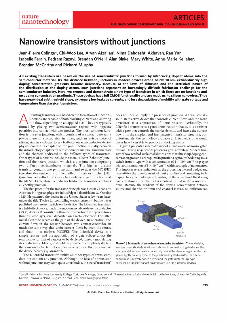
Figure 1 presents a schematic view of a junctionless nanowire gatedresistor. Having no junctions presents a great advantage. Modern tran-sistors have reached such small dimensions that ultrasharp doping con-centration gradients arerequired in junctions: typically the doping mustswitch from n-type with a concentration of 1 1019 cm23 to p-typewith a concentration of 1 1018 cm23 within a couple of nanometres.
This imposes severe limitations on the processing thermal budget andnecessitates the development of costly millisecond annealing tech-niques. In a junctionless gated resistor, on the other hand, the doping concentration in the channel is identical to that in the source anddrain. Because the gradient of the doping concentration betweensource and channel or drain and channel is zero, no diffusion can
Source
Gate
Gateoxide
Silicon
nanowire
Drain
Figure 1 | Schematic of an n-channel nanowire transistor. The underlying
insulator layer (buried oxide) is not shown. In a classical trigate device, the
source and drain are heavily doped n-type and the channel region under the
gate is lightly doped p-type. In the junctionless gated resistor, the silicon
nanowire is uniformly doped n-type and the gate material is p-type
polysilicon. Opposite dopant polarities are use for p-channel devices.
Tyndall National Institute, University College Cork, Lee Maltings, Cork, Ireland; †Present address: Laboratoire de Microelectronique, Universite Catholique de
take place, which eliminates the need for costly ultrafast annealing techniques and allows one to fabricate devices with shorter channels.
The key to fabricating a junctionless gated resistor is the for-mation of a semiconductor layer that is thin and narrow enoughto allow for full depletion of carriers when the device is turnedoff. The semiconductor also needs to be heavily doped to allow
for a reasonable amount of current flow when the device is turnedon. Putting these two constraints together imposes the use of nano-scale dimensions and high doping concentrations. The operationprinciple of the gated resistor has recently been investigatedthrough simulations by several research groups, including theTechnische Universitat Munchen, Carnegie Mellon University,IMEC and the Tyndall National Institute. The different teamsused different names for their devices: vertical slit field-effecttransistor (VeSFET)3, nanowire pinch-off FET4,5 or junctionlessmultigate field-effect transistor6, but all these devices rely on thesame basic principle of operation. More generally, the nanowirestructure is steadily gaining acceptance as the best option forfuture nanoscale transistor fabrication7–10.
An extremely simple transistor fabrication process
Silicon-on-insulator (SOI) technology can be used to producehigh-quality, single-crystal silicon films with a thickness of a few nanometres. Using commercial SOI wafers and electron-beam litho-graphy, we have defined silicon nanowires (or nanoribbons) a few tens of nanometres wide and 10 nm thick. After growing a 10-nmgate oxide, the nanowires were uniformly doped by ion implan-tation, using arsenic to dope the n-type devices and BF
2 to dope
the p-type devices. The implant energies and doses were chosento yield uniform doping concentrations ranging from of 2 1019
to 5 1019 atoms cm23 in different wafers. Such high doping levels are traditionally reserved for source and drain extension for-mation in CMOS devices. In the gated resistor, high doping isrequired to ensure a high current drive and good source anddrain contact resistance; it also imposes the use of nanowire
geometries small enough to allow for the full depletion of thechannel region, which is necessary to turn the device off. The gatewas formed by deposition of a 50-nm-thick layer of amorphoussilicon at a temperature of 550 8C in a low-pressure chemical vapour deposition (LPCVD) reactor. After heavy Pþ or Nþ gatedoping using boron or arsenic ions at a dose of 2 1014 cm22,the samples were annealed in a nitrogen ambient at 900 8C for30 min to activate the doping impurities and transform the amor-
phous silicon gate material in polycrystalline silicon. The gateelectrodes were then patterned and etched in a reactive-ion etch(RIE) reactor. Figure 2 shows a transmission electron micrographof five parallel silicon gated resistor nanoribbons with a commonpolysilicon gate electrode. The magnified view of a single nano-ribbon device is also shown (Fig. 2b), in which individual siliconatomic rows can be observed. To obtain desirable values for thethreshold voltage, a pþ polysilicon gate is used for the n-typedevice and an nþ polysilicon gate is used for the p-channeldevice. After gate patterning, a protective SiO
2 layer was deposited,
contact holes were etched, and a classical TiW–aluminium metalli-zation process was used to provide electrical contact to the devices.No doping step was performed after gate patterning, leaving thesource and drain terminals with exactly the same doping type andconcentration as the channel region. The device has a multigate
(trigate, to be more specific) configuration, which means that thegate electrode is wrapped along three edges of the device (left, topand right sides of the nanoribbon)11,12. Classical trigate FETs werefabricated on separate wafers for comparison purposes. The fabri-cation process was identical to that used for the gated resistorswith the following exceptions. The channel region was either leftundoped or was p-type doped to a concentration of 2 1017 cm23
(we consider here n-channel devices), nþ polysilicon was usedas the gate material, and arsenic ions were implanted at a dose of 2 1014 cm22 with an energy of 15 keV after gate patterning toform the source and drain junctions.
Properties that rival those of the best MOS transistorsThe current–voltage characteristics of the gated resistor are remark-
ably similar, indeed near identical, to those of a regular MOSFET.Figure 3 shows the drain current, I D
, versus gate voltage, V G
, for adrain voltage of +1 V in n-type and p-type devices having awidth of 30 nm and a length of 1 mm. The off current is below
−1.5 −1.0 −0.5 0.0 0.5 1.0 1.510−15
10−13
10−11
10−9
10−7
10−5
=1.0V
=0.05V=−0.05V
=−1.0V
D r a i n c u r r e n t ( A )
Gate voltage (V)
n-type gated resistor
p-type gated resistor
Trigate FET
Figure 3 | Current–voltage characteristics. Drain current versus gate voltage
for drain voltages of +50 mV and+1 V. The off current is below the
detection limit of the measurement system (1 10215 A), and the on/off
current ratio for between V G¼0 and V
G¼+1 V is larger than 1 106. The
width of the device is 30 nm. The curve for a classical trigate FET is shown
for comparison.
Polysilicon gate
Buried oxide
Silicon
nanoribbons
200 nm
a
b
10 nm
30.5 nm
Figure 2 | Transmission electron micrograph of silicon gated resistor
nanoribbons. a, Five parallel devices with a common polysilicon gate
electrode. b, Magnification of a single nanoribbon device. Individual atomic
the detection limit of the measurement system (1 10215 A), andthe on/off current ratio for between V
G¼ 0 and V
G¼+1 V is
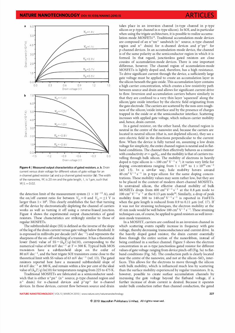
larger than 1 106. This clearly establishes the fact that turning off the device by electrostatically depleting the channel of carriersworks as well as turning it off using a reverse-biased junction.Figure 4 shows the experimental output characteristics of gatedresistors. These characteristics are strikingly similar to those of regular MOSFETs.
The subthreshold slope (SS) is defined as the inverse of the slopeof the log of the drain current versus gate voltage below threshold. It
is expressed in millivolts per decade (mV dec21) and represents thesharpness of the on–off switching of a transistor. It has a theoreticallower (best) value of SS¼ (k
BT /q) ln(10), corresponding to the
numerical value of 60 mV dec21 at T ¼ 300 K. Typical bulk MOStransistors have a subthreshold slope on the order of 80 mV dec21, and the best trigate SOI transistors come close to thetheoretical limit with SS values of 63 mV dec21 (ref. 13). The gatedresistors reported here have a measured subthreshold slope of 64 mV dec21 at 300 K, and remain within a few per cent of the ideal value of (k
BT /q) ln(10) for temperatures ranging from 225 to 475 K.
Traditional MOSFETs are fabricated as a semiconductor sand-wich that is either nþpnþ (nþ source, p-type channel region andnþ drain) for n-channel devices and pþnpþ for n-channeldevices. In those devices, current flow between source and drain
takes place in an inversion channel (n-type channel in p-typesilicon or p-type channel in n-type silicon). In SOI, and in particularwhen using the trigate architecture, it is possible to realize accumu-lation-mode MOSFETs14. Traditional accumulation-mode devicesare composed of an nþnnþ sandwich (nþ source, n-type channelregion and nþ drain) for n-channel devices and pþppþ forp-channel devices. In an accumulation-mode device, the channelis of the same polarity as the semiconductor region in which it is
formed. In that regard, junctionless gated resistors are closecousins of accumulation-mode devices. There is one importantdifference, however. The channel region of accumulation-modeMOSFETs is lightly doped and, therefore, has a high resistance.To drive significant current through the device, a sufficiently largegate voltage must be applied to create an accumulation layer inthe silicon beneath the gate oxide. This accumulation layer containsa high carrier concentration, which creates a low-resistivity pathbetween source and drain and allows for significant current driveto flow. Inversion and accumulation carriers behave similarly inthat they are confined to a very thin layer ‘squeezed’ along thesilicon/gate oxide interface by the electric field originating fromthe gate electrode. The carriers are scattered by the non-zero rough-ness of the silicon/oxide interface and by the presence of chargestrapped in the oxide or at the semiconductor interface. Scattering
increases with applied gate voltage, which reduces carrier mobility and, hence, drain current.
In a gated resistor, on the other hand, the channel region isneutral in the centre of the nanowire and, because the carriers arelocated in neutral silicon (that is, not depleted silicon), they see azero electric field in the directions perpendicular to the currentflow. When the device is fully turned on, assuming a low drain voltage for simplicity, the entire channel region is neutral and in flat-band conditions. The channel then effectively behaves as a resistorwith conductivity s ¼ qm N
D, and the mobility is that of carriers tra-
velling through bulk silicon. The mobility of electrons in heavily doped n-type silicon is 100 cm2 V21 s21; it varies very little fordoping concentrations ranging from 1 1019 to 1 1020 cm22
(ref. 15). In a similar way, hole mobility hovers around
40 cm2
V21
s21
in p-type silicon for the same doping concen-trations. These mobility values may seem rather low, but they areto be placed in the context of modern short-channel MOSFETs.In unstrained silicon, the effective channel mobility of bulk MOSFETs drops from 400 cm2 V21 s21 at the 0.8 mm node to100 cm2 V21 s21 at the 0.13 mm node16. Similarly, a drop of peak mobility from 300 to 140 cm2 V21 s21 is reported in FinFETswhen the gate length is reduced from 0.9 to 0.11 mm (ref. 17). If it was not for straining techniques, the electron mobility at the45 nm node would be well below 100 cm2 V21 s21. These straining techniques can, of course, be applied to gated resistors as well inver-sion-mode transistors.
In a MOSFET, carriers are confined in an inversion channel inwhich scattering events rapidly increase in frequency with gate voltage, thereby decreasing transconductance and current drive. In
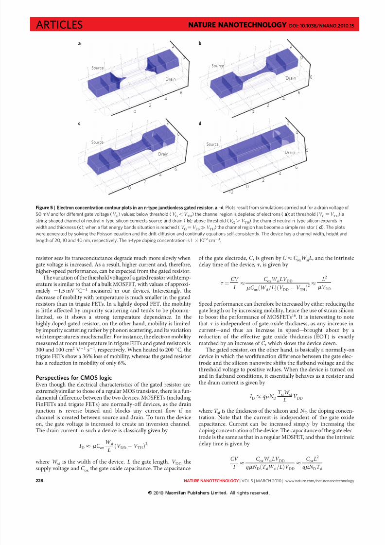
the heavily doped gated resistor, the drain current essentially flows through the entire section of the nanoribbon, instead of being confined in a surface channel. Figure 5 shows the electronconcentration in an n-type junctionless gated resistor for different values of gate voltage ranging from device pinch-off (Fig. 5a) to flat-band conditions (Fig. 5d). The conduction path is clearly locatednear the centre of the nanowire, and not at the silicon–SiO
2 inter-
faces. This allows for the electrons to move through the siliconwith bulk mobility, which is influenced much less by scattering than the surface mobility experienced by regular transistors. It is,however, possible to create surface accumulation channels by increasing the gate voltage beyond the flatband voltage, if afurther increase of drain current is desired. Because it operatesunder bulk conduction rather than channel conduction, the gated
resistor sees its transconductance degrade much more slowly whengate voltage is increased. As a result, higher current and, therefore,higher-speed performance, can be expected from the gated resistor.
The variation of the threshold voltageof a gated resistor withtemp-
erature is similar to that of a bulk MOSFET, with values of approxi-mately 21.5 mV 8C21 measured in our devices. Interestingly, thedecrease of mobility with temperature is much smaller in the gatedresistors than in trigate FETs. In a lightly doped FET, the mobility is little affected by impurity scattering and tends to be phonon-limited, so it shows a strong temperature dependence. In thehighly doped gated resistor, on the other hand, mobility is limitedby impurity scattering rather by phonon scattering, and its variationwith temperatureis muchsmaller. For instance, the electron mobility measured at room temperature in trigate FETs and gated resistors is300 and 100 cm2 V21 s21, respectively. When heated to 200 8C, thetrigate FETs show a 36% loss of mobility, whereas the gated resistorhas a reduction in mobility of only 6%.
Perspectives for CMOS logicEven though the electrical characteristics of the gated resistor areextremely similar to those of a regular MOS transistor, there is a fun-damental difference between the two devices. MOSFETs (including FinFETs and trigate FETs) are normally-off devices, as the drain junction is reverse biased and blocks any current flow if nochannel is created between source and drain. To turn the deviceon, the gate voltage is increased to create an inversion channel.The drain current in such a device is classically given by
I D m C ox
W si
L V DD V THð Þ2
where W si
is the width of the device, L the gate length, V DD
thesupply voltage and C
ox the gate oxide capacitance. The capacitance
of the gate electrode, C , is given by C C ox
W si
L, and the intrinsicdelay time of the device, t , is given by
t ¼CV
I
C ox W siLV DD
m C ox ðW si=LÞðV DD V THÞ2
L2
m V DD
Speed performance can therefore be increased by either reducing thegate length or by increasing mobility, hence the use of strain siliconto boost the performance of MOSFETs16. It is interesting to notethat t is independent of gate oxide thickness, as any increase incurrent—and thus an increase in speed—brought about by areduction of the effective gate oxide thickness (EOT) is exactly matched by an increase of C , which slows the device down.
The gated resistor, on the other hand, is basically a normally-ondevice in which the workfunction difference between the gate elec-trode and the silicon nanowire shifts the flatband voltage and thethreshold voltage to positive values. When the device is turned onand in flatband conditions, it essentially behaves as a resistor and
the drain current is given by
I D qm N DT siW si
L V DD
where T si
is the thickness of the silicon and N D
the doping concen-tration. Note that the current is independent of the gate oxidecapacitance. Current can be increased simply by increasing thedoping concentration of the device. The capacitance of the gate elec-trode is the same as that in a regular MOSFET, and thus the intrinsicdelay time is given by
CV
I
C ox W siLV DD
qm N DðT siW si=LÞV DD
C ox L
2
qm N DT si
Source
a b
c d
Drain
Source
Drain
Source
Drain
Source
2
0
6
4
2
0
Drain
2
0
6
0
4
2
0
2
0
0
6
4
2
0
−2
2
0
6
4
2
0
Figure 5 | Electron concentration contour plots in an n-type junctionless gated resistor. a–d, Plots result from simulations carried out for a drain voltage of
50 mV and for different gate voltage (V G
) values: below threshold (V G,V
TH) the channel region is depleted of electrons (a); at threshold (V
G¼V
TH) a
string-shaped channel of neutral n-type silicon connects source and drain (b); above threshold (V G.V
TH) the channel neutral n-type silicon expands in
width and thickness (c); when a flat energy bands situation is reached (V G¼V
FB V
TH) the channel region has become a simple resistor ( d). The plots
were generated by solving the Poisson equation and the drift-diffusion and continuity equations self-consistently. The device has a channel width, height and
length of 20, 10 and 40 nm, respectively. The n-type doping concentration is 1 1019 cm23.
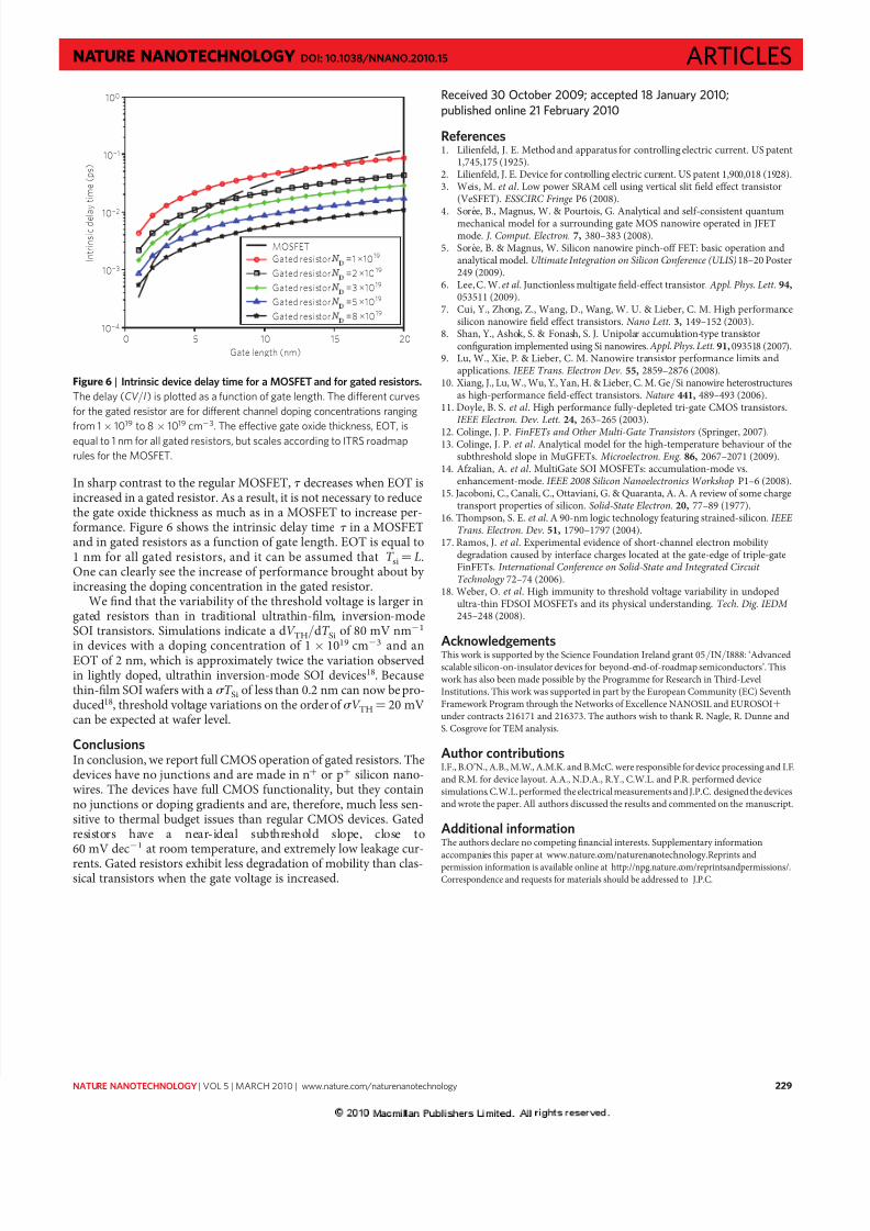
In sharp contrast to the regular MOSFET, t decreases when EOT isincreased in a gated resistor. As a result, it is not necessary to reducethe gate oxide thickness as much as in a MOSFET to increase per-formance. Figure 6 shows the intrinsic delay time t in a MOSFETand in gated resistors as a function of gate length. EOT is equal to1 nm for all gated resistors, and it can be assumed that T
si¼ L.
One can clearly see the increase of performance brought about by increasing the doping concentration in the gated resistor.
We find that the variability of the threshold voltage is larger ingated resistors than in traditional ultrathin-film, inversion-modeSOI transistors. Simulations indicate a dV
TH/dT
Si of 80 mV nm21
in devices with a doping concentration of 1 1019
cm23
and anEOT of 2 nm, which is approximately twice the variation observedin lightly doped, ultrathin inversion-mode SOI devices18. Becausethin-film SOI wafers with a s T
Si of less than 0.2 nm can now be pro-
duced18, threshold voltage variations on the order of s V TH¼ 20 mV
can be expected at wafer level.
ConclusionsIn conclusion, we report full CMOS operation of gated resistors. Thedevices have no junctions and are made in nþ or pþ silicon nano-wires. The devices have full CMOS functionality, but they containno junctions or doping gradients and are, therefore, much less sen-sitive to thermal budget issues than regular CMOS devices. Gatedresistors have a near-ideal subthreshold slope, close to60 mV dec21 at room temperature, and extremely low leakage cur-
rents. Gated resistors exhibit less degradation of mobility than clas-sical transistors when the gate voltage is increased.
Received 30 October 2009; accepted 18 January 2010;
published online 21 February 2010
References1. Lilienfeld, J. E. Method and apparatus for controlling electric current. US patent
1,745,175 (1925).2. Lilienfeld, J. E. Device for controlling electric current. US patent 1,900,018 (1928).3. Weis, M. et al . Low power SRAM cell using vertical slit field effect transistor
(VeSFET). ESSCIRC Fringe P6 (2008).
4. Soree, B., Magnus, W. & Pourtois, G. Analytical and self-consistent quantummechanical model for a surrounding gate MOS nanowire operated in JFETmode. J. Comput. Electron. 7, 380–383 (2008).
5. Soree, B. & Magnus, W. Silicon nanowire pinch-off FET: basic operation andanalytical model. Ultimate Integration on Silicon Conference (ULIS) 18–20 Poster249 (2009).
6. Lee, C. W. et al . Junctionless multigate field-effect transistor. Appl. Phys. Lett. 94,053511 (2009).
7. Cui, Y., Zhong, Z., Wang, D., Wang, W. U. & Lieber, C. M. High performancesilicon nanowire field effect transistors. Nano Lett. 3, 149–152 (2003).
8. Shan, Y., Ashok, S. & Fonash, S. J. Unipolar accumulation-type transistorconfiguration implemented using Si nanowires. Appl. Phys. Lett.91,093518 (2007).
9. Lu, W., Xie, P. & Lieber, C. M. Nanowire transistor performance limits andapplications. IEEE Trans. Electron Dev. 55, 2859–2876 (2008).
10. Xiang, J., Lu, W., Wu, Y., Yan, H. & Lieber, C. M. Ge/Si nanowire heterostructuresas high-performance field-effect transistors. Nature 441, 489–493 (2006).
11. Doyle, B. S. et al . High performance fully-depleted tri-gate CMOS transistors.IEEE Electron. Dev. Lett. 24, 263–265 (2003).
12. Colinge, J. P. FinFETs and Other Multi-Gate Transistors (Springer, 2007).13. Colinge, J. P. et al . Analytical model for the high-temperature behaviour of the
subthreshold slope in MuGFETs. Microelectron. Eng. 86, 2067–2071 (2009).14. Afzalian, A. et al . MultiGate SOI MOSFETs: accumulation-mode vs.
enhancement-mode. IEEE 2008 Silicon Nanoelectronics Workshop P1–6 (2008).15. Jacoboni, C., Canali, C., Ottaviani, G. & Quaranta, A. A. A review of some charge
transport properties of silicon. Solid-State Electron. 20, 77–89 (1977).16. Thompson, S. E. et al . A 90-nm logic technology featuring strained-silicon. IEEE
Trans. Electron. Dev. 51, 1790–1797 (2004).17. Ramos, J. et al . Experimental evidence of short-channel electron mobility
degradation caused by interface charges located at the gate-edge of triple-gateFinFETs. International Conference on Solid-State and Integrated Circuit Technology 72–74 (2006).
18. Weber, O. et al . High immunity to threshold voltage variability in undopedultra-thin FDSOI MOSFETs and its physical understanding. Tech. Dig. IEDM 245–248 (2008).
AcknowledgementsThis work is supported by the Science Foundation Ireland grant 05/IN/I888: ‘Advanced
scalable silicon-on-insulator devices for beyond-end-of-roadmap semiconductors’. This
work has also been made possible by the Programme for Research in Third-Level
Institutions. This work was supported in part by the European Community (EC) Seventh
Framework Program through the Networks of Excellence NANOSIL and EUROSOIþ
under contracts 216171 and 216373. The authors wish to thank R. Nagle, R. Dunne and
S. Cosgrove for TEM analysis.
Author contributionsI.F., B.O’N., A.B., M.W., A.M.K. and B.McC. were responsible for device processing and I.F.
and R.M. for device layout. A.A., N.D.A., R.Y., C.W.L. and P.R. performed device
simulations. C.W.L. performed the electrical measurements and J.P.C. designed the devices
and wrote the paper. All authors discussed the results and commented on the manuscript.
Additional informationThe authors declare no competing financial interests. Supplementary information
accompanies this paper at www.nature.com/naturenanotechnology. Reprints and
permission information is available online at http://npg.nature.com/reprintsandpermissions/.Correspondence and requests for materials should be addressed to J.P.C.
MOSFET
Gated resistor =1 ×10¹⁹
Gated resistor =2 ×10¹⁹
Gated resistor =3 ×10¹⁹
Gated resistor =5 ×10¹⁹
Gated resistor =8 ×10¹⁹
0 5 10 15 20
Gate length (nm)
I n t r i n s i c d e l a y t i m e ( p s )
10−4
10−3
10−2
10−1
100
Figure 6 | Intrinsic device delay time for a MOSFET and for gated resistors.
The delay (CV /I) is plotted as a function of gate length. The different curves
for the gated resistor are for different channel doping concentrations ranging
from 1
1019 to 8
1019 cm23. The effective gate oxide thickness, EOT, is
equal to 1 nm for all gated resistors, but scales according to ITRS roadmap