HAL Id: hal-00793916 https://hal.archives-ouvertes.fr/hal-00793916 Submitted on 10 Jun 2013 HAL is a multi-disciplinary open access archive for the deposit and dissemination of sci- entific research documents, whether they are pub- lished or not. The documents may come from teaching and research institutions in France or abroad, or from public or private research centers. L’archive ouverte pluridisciplinaire HAL, est destinée au dépôt et à la diffusion de documents scientifiques de niveau recherche, publiés ou non, émanant des établissements d’enseignement et de recherche français ou étrangers, des laboratoires publics ou privés. Diffusion Mechanism of Lithium Ion through Basal Plane of Layered Graphene Fei Yao, Fethullah Gunes, Hui Quang Ta, Seung Mi Lee, Seung Jin Chae, Kyeu Yoon Sheem, Costel Sorin Cojocaru, Si Shen Xie, Young Hee Lee To cite this version: Fei Yao, Fethullah Gunes, Hui Quang Ta, Seung Mi Lee, Seung Jin Chae, et al.. Diffusion Mechanism of Lithium Ion through Basal Plane of Layered Graphene. Journal of the American Chemical Society, American Chemical Society, 2012, 134 (20), pp.8646–8654. 10.1021/ja301586m. hal-00793916
Transcript
HAL Id: hal-00793916https://hal.archives-ouvertes.fr/hal-00793916
Submitted on 10 Jun 2013
HAL is a multi-disciplinary open accessarchive for the deposit and dissemination of sci-entific research documents, whether they are pub-lished or not. The documents may come fromteaching and research institutions in France orabroad, or from public or private research centers.
L’archive ouverte pluridisciplinaire HAL, estdestinée au dépôt et à la diffusion de documentsscientifiques de niveau recherche, publiés ou non,émanant des établissements d’enseignement et derecherche français ou étrangers, des laboratoirespublics ou privés.
Diffusion Mechanism of Lithium Ion through BasalPlane of Layered Graphene
Fei Yao, Fethullah Gunes, Hui Quang Ta, Seung Mi Lee, Seung Jin Chae,Kyeu Yoon Sheem, Costel Sorin Cojocaru, Si Shen Xie, Young Hee Lee
To cite this version:Fei Yao, Fethullah Gunes, Hui Quang Ta, Seung Mi Lee, Seung Jin Chae, et al.. Diffusion Mechanismof Lithium Ion through Basal Plane of Layered Graphene. Journal of the American Chemical Society,American Chemical Society, 2012, 134 (20), pp.8646–8654. �10.1021/ja301586m�. �hal-00793916�
Diffusion Mechanism of Lithium Ion through Basal Plane of Layered Graphene
Fei Yao,a,d Fethullah Gunes, a Huy Quang Ta, a Seung Mi Lee,b Seung Jin Chae,a Kyeu Yoon Sheem,c
Costel Sorin Cojocaru,d Si Shen Xie,a and Young Hee Lee,a
a Department of Energy Science, BK21 Physics Division, Graphene Center, Sungkyunkwan Advanced Institute of Nanotechnology, Sungkyunkwan University, Suwon 440-746, Republic of South Korea
bCenter for Nanocharacterization, Korea Research Institute of Standards and Science, Daejeon 305-340, Republic of South Korea
cSamsung SDI Corporate R&D Center, Gongse-dong, Giheung-gu, Yongin-si, Gyeounggi-do 446-577, Republic of South Korea
dLPICM CNRS, Ecole polytechnique, Palaiseau 91120, France
ABSTRACT: Coexistence of both edge plane and basal plane in graphite often hinders the understanding of lithium ion diffusion mechanism. In this report, two types of graphene samples were prepared by chemical vapor deposition (CVD): (i) well-defined basal plane graphene grown on Cu foil and (ii) edge plane-enriched graphene layers grown on Ni film. Electrochemical performance of the graphene electrode can be split into two regimes depending on the number of graphene layers: (i) the corrosion-dominant regime and (ii) the lithiation-dominant regime. Li ion diffusion perpendicular to the basal plane of graphene is facilitated by defects, whereas diffusion parallel to the plane is limited by the steric hindrance that originates from aggregated Li ions adsorbed on the abundant defect sites. The critical layer thickness (lc) to effectively prohibit substrate reaction using CVD-grown graphene layers was predicted to be ∼6 layers, independent of defect population. Our density functional theory calculations demonstrate that divacancies and higher order defects have reasonable diffusion barrier heights allowing lithium diffusion through the basal plane but neither monovacancies nor Stone-Wales defect.
INTRODUCTION Graphite has been widely used as an anode material in lithium ion batteries due to its well-defined layered structure for lithium intercalation, low operating potential, and remarkable interfacial stability.1 Graphite has two characteristic planes: a basal plane and an edge plane, which are parallel and perpendicular to the c-axis, respectively. It is known in general that the basal plane and edge plane exhibit different physical and chemical activities in many aspects, leading to different lithiation capabilities in graphite.2,3 The diffusion time constant for Li ion insertion within the active graphitic flakes is governed by the formula τ = L2/2D, where L is the diffusion length (or radius of spherical flake) and D is diffusion coefficient.4 Although lithium diffusion through basal plane is rather limited, lithium diffusion may still occur through several defect sites, such as vacancies and grain boundaries.5,6 Lithium diffusion through an edge plane of graphitic flakes can be easily facilitated but is further complicated by the presence of different functional groups such as hydroxyl and carboxyl groups. In other words, lithiation through these two different planes is highly anisotropic.5−9 One ambiguity in understanding a diffusion pathway of lithium ions in graphite is the coexistence of both edge planes and basal planes in the sample. The presence of these two different interfaces is unavoidable in conventional graphite.10,11 Currently available highly oriented pyrolytic graphite (HOPG), which is well-known as a highly ordered crystallographic structure, has a finite size of flakes whose edge planes are still abundant in addition to basal planes. Therefore, lithium ion diffusion through the basal plane cannot be exclusively observed.5−8 Thus, a well-defined basal plane of graphite with a large area is required to have a comprehensive picture of lithium diffusion mechanism in lithium ion batteries. Recently, large area monolayer and multilayer graphene have been synthesized by chemical vapor deposition (CVD).12,13 This paves a new route for exploring numerous new fundamental sciences and, moreover, developing numerous technological breakthroughs in electronics and energy storage.14−16 Large area graphene can be transferred onto any substrate by a simple transfer process and therefore an anode electrode with layered graphene without leaving an edge plane (or negligible portion of edge plane) is easily attainable. This provides an opportunity to study the diffusion of lithium ions exclusively through the basal plane of graphene. However, in lithium ion batteries, corrosion of the conventional current collectors such as Al, Cu, and stainless steel (SUS) can adversely affect lifetime and safety through increased internal resistance, passivation of active materials, and consumption of electrolyte/active electrode materials.17−23 Anode performance of thin graphene layers can be misguided by the strong substrate reaction since the most reactive lithium ions exist in electrolyte.24,25 It has been proposed that monolayer graphene can be used as a protective layer for substrate against air oxidation and mild electrochemical mechanically polished with FeCl3
solution for flattening. The prepared Cu foil was then brought into the growth chamber. The temperature of the chamber was heated up to 1060 °C with 1000 sccm of Ar gas and 200 sccm of H2 gas for 20 min. Methane (5 sccm) was then introduced with 10 sccm H2 gas for 5 min. After growth, the sample was cooled to room temperature naturally in the same atmosphere. In the case of MLG synthesis, Ni thin film (300 nm) was deposited on SiO2 (300 nm)/Si by a thermal evaporator. This was placed in rapid thermal CVD chamber. The temperature was increased to 1000 °C in reaction.26,27 Therefore, information on the critical layer 5 min in vacuum. Ni surface was reduced by flowing 45 sccm H2 gas at thickness of graphene (lc) to minimize the substrate effect and the influence of defects to lc are key ingredients to understand electrochemical reaction and protective nature of graphene layers under severe electrochemical condition. The main purpose of this work is two-fold: (i) To clarify the lithium diffusion pathway through the basal plane of graphene layers and (ii) to investigate the influence of defect population to lithium ion diffusion and the protective ability of graphene layers. In this work, we prepared Cu-grown monolayer graphene (SLG) samples and Ni-grown multilayered graphene (MLG) samples that are dominated with graphene basal planes and edge planes, respectively. We found that the electro- chemical performance of few-layer graphenes (FLGs) which are overlapped up to three layers of SLG is strongly affected by the substrate reaction. Experiments with Ar plasma treatment 1000 °C. The gas mixing ratio of C2H2/H2 was optimized to 2:45 sccm and flown for 1 min. After completion of growth, the gas supply was terminated, and the chamber was cooled to room temperature. The detail has been described elsewhere.28,29 Transfer Process of a Graphene. PMMA (e-beam resist, 950 k C4, Microchem) was spin-coated on the graphene/Cu foil (Ni film) at 1000 rpm for 60 s. To etch away Cu foil (Ni film), the sample was submerged in a copper etchant (CE-100, Transene) for ∼30 min (4 h for Ni film). After rinsing by deionized water for a few times, the PMMA/graphene layer was fished onto the CR 2032 cell case coated with lithium-reaction resistive polymer. PMMA was removed by acetone later after graphene was completely dried and attached onto the cell case. The transferred sample was then annealed up to 650 °C for 5 h in high vacuum (1 × 10⁻⁶ Torr) for further removal of PMMA.30 Argon Plasma Treatment of Graphene. Structural defects of indicated that 6 layers of basal plane-enriched large area graphene were created by Ar+ bombardment with different plasma graphene were needed to provide effective substrate protection. Combing the experimental results and density functional theory calculations, we proved that basal plane hindered lithium ion diffusion with a high diffusion barrier height, whereas divacancies and higher order defects can be shortcuts for lithium ion diffusion.
Figure 1. Schematic of a coin cell fabrication process with Cu-grown SLG or Ni-grown MLG. Bilayer and trilayer graphene coin cells were fabricated by repeatedly transferring monolayer graphene.
EXPERIMENTAL SECTION Material Synthesis. Large area SLG was synthesized on copper foil by atmospheric pressure (AP) CVD. Cu foil purchased from Nilaco (Lot No. 113321, 99.96%, 100 μm in thickness) was preannealed to 1060 °C for 2 h with 100 sccm of Ar gas and 200 sccm of H2 gas to enlarge Cu grain
size and then chemico- powers (15 W, 100 W) for 1 min. The transferred graphene was brought into the vacuum chamber with a base pressure of 1 × 10⁻⁶ Torr and then filled with Ar gas of 100 sccm for a minute, followed by the plasma ignition. This was repeated layer by layer to obtain Ar+ plasma-treated FLG samples. Material Characterization. For optical images and confocal Raman spectroscopy, the CRM 200 (WiTec, Germany) with 100 lens (Olympus, N. A. 0.9) and ∼1 mW of 532 nm laser was used. For micro-Raman spectroscopy (Renishaw, RM-1000 Invia) with an excitation energy of 2.41 eV (514 nm, Argon laser) and UV−vis- NIR absorption spectroscopy (Varian, Cary 5000) were used for characterizing optical properties of the graphene films on SiO2/Si and PET substrates, respectively. Electrochemical Measurement. Electrochemical measurements were performed with a CR2032 coin cell using VMP3 instrument (BioLogic Science Instruments). The cell was assembled in a dry room using the CR 2032 cell case with different number of graphene layers and bare foil (SUS 316) as a working electrode, lithium metal foil as a counter/reference electrode, and a 1 M of LiPF6 in a 1:1 (v/v) mixture of ethylene carbonate (EC) and diethyl carbonate (DEC) as an electrolyte. A glassy carbon microfiber was used as a separator. The cells were charged and discharged galvanostatically between 3.0 and 0.01 V at a constant current of 5 μA/cm2. The AC impedance spectra were obtained by applying a sine wave with an amplitude of 10 mV over a frequency range of 100 kHz to 10 mHz.31 Theoretical Calculation. We performed density functional theory calculations within generalized gradient approximation as implemented in DMol3 code.32,33 All electron Kohn−Sham wave functions were expanded in a local atomic orbital basis set with each basis function defined numerically on an atomic centered spherical mesh. Double numeric polarized basis sets (DNP) were used for all elements. The dangling bonds of graphene edge were saturated by hydrogen atoms and the atomic cluster structure which consists of 120 carbon atoms and 48 hydrogen atoms were relaxed fully until the force on each atom is less than 10−4 eV/Å and the total energy change is less than 5 × 10⁻⁵ eV. The dampened atom-pairwise dispersion corrections of the form C6R−6 were also considered for calculations.34 Li adsorption 0.01 to 3 V. The bare SUS electrode showed an anodic peak near 1.03 V (S ) and a cathodic peak around 0.78 V (S ). energy was calculated by Ead(Li) = Etot(Li + carbon) − Etot(Li) −Etot(carbon), where Etot(Li) is the self-energy of lithium atom and Etot(carbon) is the total energy of carbon system. Various local charges were also calculated using Mulliken, Hirshfeld, and electrostatic potential (ESP). (See also Supporting Information, SI, S5.)
Figure 2. Optical micrographs of (a) Cu-grown SLG and (b) Ni-grown MLG on SiO2/Si substrate. White dashed lines indicate wrinkles. Some portion of thicker graphene is indicated by arrows. (c) Schematic of (i) SLG with a well-defined basal plane and (ii) edge plane enriched MLG. (d) Micro-Raman spectra of SLG and MLG. Confocal Raman mapping of D/G intensity ratio of (e) SLG and (f) MLG from squared positions of (a) and (b). The contrast is normalized to 0.4 to visualize the defect distribution for both images. (g) Wavelength-dependent transmittance (values are provided at a wavelength of 550 nm) and (h) optical photographs of different number of graphene layers on PET substrate.
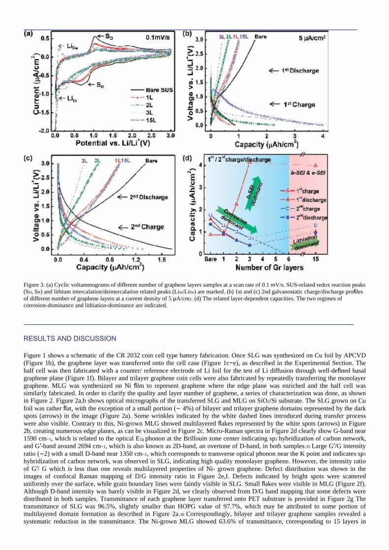
Figure 3. (a) Cyclic voltammograms of different number of graphene layers samples at a scan rate of 0.1 mV/s. SUS-related redox reaction peaks (SO, SR) and lithium intercalation/deintercalation related peaks (LiIn/LiDe) are marked. (b) 1st and (c) 2nd galvanostatic charge/discharge profiles of different number of graphene layers at a current density of 5 μA/cm2. (d) The related layer-dependent capacities. The two regimes of corrosion-dominance and lithiation-dominance are indicated.
RESULTS AND DISCUSSION Figure 1 shows a schematic of the CR 2032 coin cell type battery fabrication. Once SLG was synthesized on Cu foil by APCVD (Figure 1b), the graphene layer was transferred onto the cell case (Figure 1c−e), as described in the Experimental Section. The half cell was then fabricated with a counter/ reference electrode of Li foil for the test of Li diffusion through well-defined basal graphene plane (Figure 1f). Bilayer and trilayer graphene coin cells were also fabricated by repeatedly transferring the monolayer graphene. MLG was synthesized on Ni film to represent graphene where the edge plane was enriched and the half cell was similarly fabricated. In order to clarify the quality and layer number of graphene, a series of characterization was done, as shown in Figure 2. Figure 2a,b shows optical micrographs of the transferred SLG and MLG on SiO2/Si substrate. The SLG grown on Cu foil was rather flat, with the exception of a small portion (∼ 4%) of bilayer and trilayer graphene domains represented by the dark spots (arrows) in the image (Figure 2a). Some wrinkles indicated by the white dashed lines introduced during transfer process were also visible. Contrary to this, Ni-grown MLG showed multilayered flakes represented by the white spots (arrows) in Figure 2b, creating numerous edge planes, as can be visualized in Figure 2c. Micro-Raman spectra in Figure 2d clearly show G-band near 1590 cm−1, which is related to the optical E2g phonon at the Brillouin zone center indicating sp2 hybridization of carbon network, and G′-band around 2694 cm−1, which is also known as 2D-band, an overtone of D-band, in both samples.35 Large G′/G intensity ratio (∼2) with a small D-band near 1350 cm−1, which corresponds to transverse optical phonon near the K point and indicates sp3
hybridization of carbon network, was observed in SLG, indicating high quality monolayer graphene. However, the intensity ratio of G′/ G which is less than one reveals multilayered properties of Ni- grown graphene. Defect distribution was shown in the images of confocal Raman mapping of D/G intensity ratio in Figure 2e,f. Defects indicated by bright spots were scattered uniformly over the surface, while grain boundary lines were faintly visible in SLG. Small flakes were visible in MLG (Figure 2f). Although D-band intensity was barely visible in Figure 2d, we clearly observed from D/G band mapping that some defects were distributed in both samples. Transmittance of each graphene layer transferred onto PET substrate is provided in Figure 2g The transmittance of SLG was 96.5%, slightly smaller than HOPG value of 97.7%, which may be attributed to some portion of multilayered domain formation as described in Figure 2a.36 Correspondingly, bilayer and trilayer graphene samples revealed a systematic reduction in the transmittance. The Ni-grown MLG showed 63.6% of transmittance, corresponding to 15 layers in
average by assuming 2.3% absorption per each layer.36 Optical photographs were provided to visualize different transmittances with different numbers of graphene layers in Figure 2h. Figure 3a shows cyclic voltammograms (CV) of different numbers of graphene layers at a scan rate of 0.1 mV/s from These redox peaks involve chemical reactions with Li ions and possibly electrolytes. Both anodic and cathodic peaks were reduced in the monolayer graphene electrode. These peaks were reduced consecutively in bilayer and trilayer graphene electrodes. It is obvious to see that the redox reaction of the bare SUS electrode was suppressed by the coated graphene layers. An additional cathodic peak appeared near 0.28 V in bilayer and trilayer samples. The origin of these peaks could be ascribed to defect-associated lithium adsorption.5 At the MLG (15 layer graphenes) sample, a sharp cathodic peak near 0.01 V (LiIn) is identified as lithium intercalation and a rather broad peak near 0.12 V (LiDe) is related to decomposition of graphitic intercalation compound (GIC) stages.24 It is of note that the bare SUS-related peak was nearly compressed in this case. Both LiDe and LiIn peaks appeared in this case, in good contrast with FLG samples in which only a clear LiIn peak was observed, suggesting that no GIC stages were formed in FLGs. The distinct CV behavior of FLGs and MLG demonstrates that lithium ion intercalation becomes more effective in MLG induced by the considerable amount of edge planes, as shown in Figure 2b. Figure 3b shows the first galvanostatic charge/discharge profile with a voltage sweeping range of 0.01−3 V at a constant current of 5 μA/cm2. As the number of graphene layers increased, a long tail appeared in the charge curve at the low voltage region. At MLG sample, a plateau appeared in the range of 1.25−0.6 V. In graphitic material, the solid-electrolyte interface (SEI) formation via electrolyte decomposition takes place in the range of less than 1.0 V.7,37−39 The SEI formation potential varies with types of graphite planes. In general, SEI forms at higher potential in edge plane than in basal plane.40−42 Therefore, we ascribed this plateau in MLG to edge plane- related SEI formation. In the second cycle, the voltage profile shows a gradual change in a wide range of voltages during charge/discharge, revealing a V-shape curve, i.e., no plateau region, as shown in Figure 3c. This is in good contrast with a U- shaped curve in graphite electrode, where the edge plane intercalation is dominant in the plateau region of low voltage within 0.1 V.39,43 Capacities of graphene-coated electrodes in Figure 3c were consistently smaller than those of the bare electrode, and furthermore much smaller by about 30 times than the recently reported graphene battery result.16 The huge capacity difference comes from the use of different substrates (See Figure S1 of the SI). This implies that in spite of graphene layers coated on the electrode with well-defined basal plane, the reaction with electrode did inevitably occur. The related layer-dependent capacities are summarized in Figure 3d. As the number of graphene layers increased, the first charge capacity increased rapidly up to trilayer graphene electrode and saturated at the MLG electrode. As described in the schematic of Figure 2c, the basal plane is exposed during lithiation up to three layers, whereas both the edge plane and basal plane are present in 15 layers. Two different types of SEI are formed: (i) basal-plane associated SEI (b-SEI) which is formed up to 3 graphene layers and (ii) edge-plane associated SEI (e-SEI) which is formed in MLG sample. It has been known that b-SEI formed at lower potential is associated with solvent reduction, while e-SEI formed at higher potential is associated with salt ions.40−42,44 Since our basal plane contains abundant defect sites, as observed from Figure 2d,e, some decomposed solvent molecules may further diffuse into the subjacent layers along with Li ions or in a form of lithium salvation and form additional b-SEI layer. This is why b-SEI increases as the number of graphene layers increases at FLG samples. At the MLG electrode, both b-SEI and e-SEI are formed. Although e-SEI increases in this case, b-SEI is reduced compared to FLG electrodes due to the decrease of effective basal plane area of 15 layers (See Figure 2c) and therefore the capacity from SEI formation is saturated in the first charge. On the other hand, the first discharge capacity decreased gradually up to three layer graphene electrode and increased at 15 layer electrode. Similar trend was also observed in the second charge/discharge profile. The discharge capacities of the second cycle were not much different from those of the first cycle. A large capacity of the bare SUS electrode was reduced by coating graphene layers up to three layers. This gradual reduction was also expected from the reduced areas of CV curves in FLGs (Figure 3a). This implies several facts: (i) SUS substrate reaction is systematically suppressed with an increasing number of graphene layers (For impedance measurement of pristine graphene layers, see Figure S2 of the SI). (ii) Because lithium ions can diffuse through the basal plane of graphene, monolayer graphene is not sufficient to prohibit substrate reaction. Since the pure basal plane presumably does not allow Li diffusion, the diffusion may be provoked through some defect sites that exist on the graphene plane, as observed from the D/G intensity ratio of confocal Raman mapping in Figure 2e. This will be described later in detail. In FLG samples, if we presume capacity only to be contributed from intercalation (0.028 μAhcm−2/interlayer in the case of LiC6), then the intercalation capacity reaches 0.056 μAh/cm2 at trilayer graphene sample (see Figure S3 of the SI). This value is negligible to the capacity (0.73 μAh/cm2) observed in our experiment. This tells us that even if intercalation of lithium ions was invoked, the observation was still obscured by the dominant SUS redox reaction. By noting a linear decrease of the capacity and hence extrapolating to a minimum capacity, lc to effectively prohibit the SUS redox reaction is predicted to be ∼6 layers (See Figure S2 of the SI for the impedance measurement of 6 layer graphene sample). As the number of graphene layers increases, the capacity from the SUS redox reaction decreases, while the capacity reduction will be compensated by the intercalation capacity between graphene layers. After 6 layers, the capacity starts increasing by the pure intercalation. We can define substrate corrosion- dominant region up to 6 layers and lithiation-dominant region after 6 layers, as visualized in Figure 3d. The theoretically estimated capacity at 15 layers (or effectively 9 layers), is 0.2 μAh/cm2 (see Figure S3 of the SI). However, this value is still far smaller than the observed value of 1.30 μAh/cm2. This extra capacity could be ascribed to the lithium adsorption on defects of the graphene surface, which can be supported by the widely distributed defects observed from confocal Raman mapping in our experiments (Figure 2f). In the second cycle, the discharge capacity was consistently smaller than the charge capacity, nearly independent of the thickness of graphene layers. This difference of 0.35 μAh/cm2 in the charge/discharge capacity is irreversible capacity and can be ascribed to strongly adsorbed lithium ions on defects such as vacancies or grain boundaries formed on the graphene layers. This will be discussed in the theory section later. Since defects on graphene basal plane seem to play an important role in lithium diffusion, a systematic study is required for comprehensive analysis. Figure 4a shows Raman spectra of Ar plasma-treated monolayer graphene. At 15 W plasma power, D/G intensity ratio was increased to 0.56 from 0.19 in no plasma-treated pristine graphene, implying structural defect formation in the graphene plane. At 100 W, one additional peak near 1620 cm−1 (D′) appeared in addition to further increase of D-band intensity (D/G intensity ratio is 1.66), indicating plausible formation of structural defects.45 No peak splitting of G-band into G+ and G− peaks indicates that our process does not involve strain-induced effect.46 Figure 4b shows CV diagrams for SLG electrode with different plasma powers at a scan rate of 0.1 mV/s. (For CV diagrams of plasma- treated graphene samples with
different numbers of graphene layers, see Figure S4 of the SI.) It is obvious to see that the redox reaction peak intensities of SO and SR related peaks were enhanced and the related peak positions were also shifted after plasma treatment. Those peaks are a combination of defect- associated adsorption and SUS substrate reaction, as mentioned in Figure 3a. Additional redox reaction due to the generated basal plane defects by plasma treatment is provoked. Since the protective layer is monolayer graphene, extra lithium ions adsorbed on defects could easily reach the SUS substrate, thus increasing the substrate redox reaction. The second galvano- static charge/discharge capacity of SLG increased accordingly compared to the pristine graphene sample, as shown in Figure 4c. (For charge/discharge profiles of plasma-treated bilayer and trilayer graphene electrodes, see Figure S4 of the SI.) The enhanced capacity was attributed to the increased adsorption of Li ions on defects and increased substrate reaction, as mentioned in Figure 4b. The second charge capacity kept increasing with increasing plasma power, independent of the number of graphene layers, as summarized in Figure 4d. The substrate redox reaction was also suppressed, which is identified by the capacity decrease with increasing number of graphene layers similar to that of pristine graphene samples. Smaller capacity was increased in FLG electrodes compared to that of SLG after plasma treatment and generated different slopes, as shown in Figure 4d. The absolute slope increased from 0.26 to 0.56 with increasing the plasma power. Extrapolation of these slopes, which determines the critical layer thickness to prohibit substrate reaction, gave rise to lc of ∼6 layers independent of the plasma power, i.e., defect population. This is rather surprising, because creation of more defects in the basal plane is expected to increase basal- plane diffusion of Li ions which will eventually increase substrate redox reaction (See Figure 4b,c) and thereby larger critical layer thickness should be required after strong plasma treatment. In order to explain this contradictory phenomenon, a schematic of Li diffusion through defects in the basal plane is provided in Figure 4e. In the case of SLG, Li ion diffusion is allowed through defect sites and no lateral diffusion limitation is expected, since the graphene layer is fully surrounded by Li ions in electrolyte. Therefore, a higher defect population will enhance Li ion adsorption and also substrate reaction. In the case of FLGs, where large area basal plane is dominant, graphene layers are overlapped with each other so that Li ions will diffuse through defects perpendicular to the plane of the top layer first and diffuse along the plane of subjacent graphene layer until they meet another defect site. Since these Li ions may accumulate near the defect sites generated by Ar plasma, Li diffusion along the plane direction will be limited by the steric hindrance from aggregated Li atoms, which is different from the SLG case. Therefore, further Li diffusion through graphene basal planes in FLGs is constrained severely by the lateral diffusion at higher defect density. Thus, when FLGs are used as a protective layer, the defects-related lithium adsorption on subjacent graphene layers and actual lithium ion reaction with substrate are suppressed, which is again consistent with the reduction of the peaks in CV diagrams (See Figure S4a,b of the SI). As a consequence of these phenomena, the critical layer thickness gives rise to the same value, independent of the defect population. It will be worth mentioning the possibility of forming oxygen-related functional groups on defect sites. Li ions can also be adsorbed on such sites and thus our argument of lateral diffusion suppression by the steric hindrance is still valid.
Figure 4. (a) Raman spectra, (b) cyclic voltammograms at a scan rate of 0.1 mV/s, and (c) 2nd galvanostatic charge/discharge profiles at a current density of 5 μA/cm2 for monolayer graphene treated by Ar plasma with different plasma powers (15 and 100 W). (d) Capacity of 2nd charge as a functional of number of graphene layers under different Ar plasma powers. Absolute slopes according to different plasma powers and critical layer thickness (lc) are indicated. (e) Schematics of proposed Li diffusion mechanism through defects on the basal plane with different defect population. Broad down arrows indicate Li ion diffusion through defect sites of basal plane. Red glows represent steric hindrance for Li ion diffusion formed by the accumulated Li ions or functional groups. The inset in the right indicates the relative magnitude of diffusion coefficient. (f) Relationship of D/Gratio with the extracted slope from (d).
It is intriguing to see the relationship between D/G intensity ratio from Raman spectra and the slope extracted from charge/discharge profiles, as shown in Figure 4f. The slope which indicates Li diffusion through graphene layers is correlated to the population of defects in the graphene plane. The larger slope implies the slower diffusion rate and vice versa. Li ion diffusion is limited by the Li aggregates adsorbed on the increased defect sites described in the schematic (e). Thus, information of Li diffusion obtained from electrochemical test could be used as a metric for evaluating the defect population of graphene, an
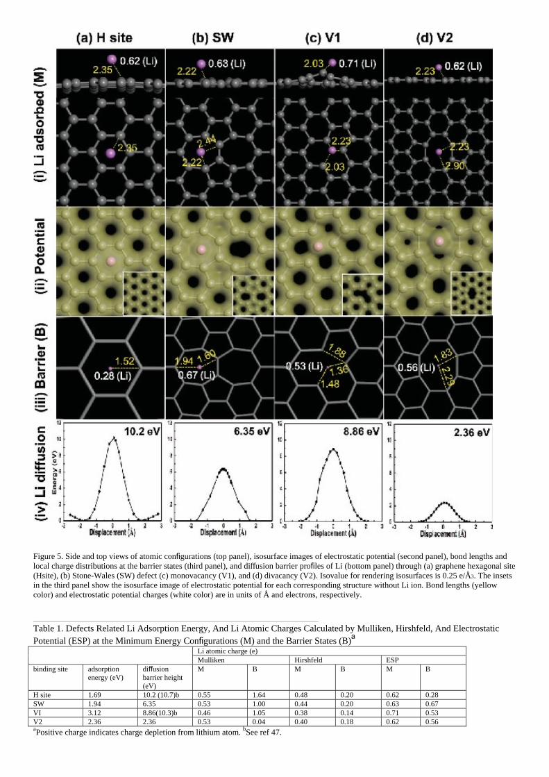
important material parameter of graphene. In order to understand what type of defects allows Li ion diffusion through the basal plane of graphene, we conducted density functional theory calculations for various defects: ideal hexagonal site (H site), Stone−Wales defect (SW), mono- vacancy (V1), and divacancy (V2). Li atom adsorbs on the H site with a bond length of 2.35 Å above the graphene plane and with an adsorption energy of −1.69 eV, as shown in the upper panel of Figure 5a and Table 1. Li ESP charge at H site is partially depleted to 0.62 e. The ESP charge of Li atom at barrier state is 0.28 e, much less compared to that at the binding site (see Figure S5 of the SI for details). This charge difference between adsorption and barrier state is an important variable in determining the Coulomb interaction energy. As the Li approaches to the barrier site, the available space for Li is narrow with a short separation distance of 1.52 Å, invoking severe charge overlapping between Li and adjacent carbon atoms, as can be seen in the electrostatic potential contour in the second panel of Figure 5a. This increases repulsive forces, giving rise to large diffusion barrier height of 10.2 eV, similar to the previous report (Table 1),47 validating our approaches.48 A similar situation takes place in the SW defect, which is abundant in the graphene grain boundary.49 The Li adsorption energy near the heptagon is −1.94 eV, slightly stronger than that of H site. Although the charge overlapping is still severe, a longer separation distance of 1.60 Å and also much less charge difference between adsorption and barrier state (0.04 e) forms a relatively smaller activation barrier height of 6.35 eV than that of H site, as shown in Figure 5b. In the case of V1, Li adsorbs at the vacancy site with an adsorption energy of −3.12 eV, keeping closer distance (2.03 Å), as shown in the top panel of Figure 5c. The excess charge difference of Li atom between adsorption and barrier site is 0.18 e and the closest separation distance at the barrier site is 1.36 Å. Charges are distributed not only on the Li and carbon sites, but also between them, implying both covalent bonding and ionic bonding characters due to charge depletion from Li atom. This produces a large diffusion barrier height of 8.86 eV. However, V2 provides a rather large open space with an adsorption energy of −2.36 eV near the middle of the two dimers (top panel of Figure 5d) such that a large separation distance of 2.90 Å is maintained. This gives minimizes electrostatic charge overlapping and a large bond length of 1.83 Å at the barrier state, i.e., steric hindrance is minimized, as shown in the second and third panels in Figure 5d. The charge difference between the adsorption and the barrier states is 0.04 e. All of these factors induced a smallest diffusion barrier height (2.36 eV) among the defects we studied. This barrier height can be overcome under the typical charging conditions of the battery.
Figure 5. Side and top views of atomic configurations (top panel), isosurface images of electrostatic potential (second panel), bond lengths and local charge distributions at the barrier states (third panel), and diffusion barrier profiles of Li (bottom panel) through (a) graphene hexagonal site (Hsite), (b) Stone-Wales (SW) defect (c) monovacancy (V1), and (d) divacancy (V2). Isovalue for rendering isosurfaces is 0.25 e/Å3. The insets in the third panel show the isosurface image of electrostatic potential for each corresponding structure without Li ion. Bond lengths (yellow color) and electrostatic potential charges (white color) are in units of Å and electrons, respectively.
Table 1. Defects Related Li Adsorption Energy, And Li Atomic Charges Calculated by Mulliken, Hirshfeld, And Electrostatic Potential (ESP) at the Minimum Energy Configurations (M) and the Barrier States (B)a Li atomic charge (e)
We have studied lithium diffusion pathways with two types of graphene samples prepared by CVD; (i) well-defined basal plane graphene grown on Cu foil and (ii) edge plane-enriched graphene layers grown on Ni film. We have discovered that electrochemical reaction of the electrode (substrate/graphene) is not only related to the number of graphene layers but also relies on the defect sites on the basal plane of graphene. The experimental and calculated results related to the specific types of defects, such as divacancies and higher order defects, that can assist lithium ion diffusion through the basal plane could help us in designing high capacity and highly conductive corrosion- free electrodes for lithium ion batteries. It would be reasonable to expect that the substrate-protective nature of few-layer graphenes could be the basis for further investigation of the preparation of original substrate, which remains unaltered with respect to its properties and has a longer lifetime under the severe electrochemical corrosion conditions found in batteries. Furthermore, by correlating the lithium diffusion in graphene layers to the D/G intensity ratio from Raman spectra, we developed a way of predicting the defect population of graphene with an electrochemical method.
* Supporting Information
Figures showing the corrosion effect of different types of SUS substrate, AC impedance spectra of pristine graphene samples, relationship between intercalation capacity and different numbers of graphene layers, cyclic voltammogram and 2nd charge/discharge behavior of graphene samples with different number of layers under different plasma powers, charges (Li site) calculated by various models with varying the normal distance from barrier site to the stable position of Li adsorption at the H site. This material is available free of charge via the Internet at http://pubs.acs.org.
ACKNOWLEDGMENTS
This work was supported by the Star Faculty program (2010- 0029653) and WCU program (R31- 2008-10029) of the NRF of Korea funded by MEST. The density functional theory work was supported by KRCF through KRISS. Authors gratefully acknowledge Drs. Feng Li and Li Liu for valuable discussions.
REFERENCES
(1) Winter, M.; Besenhard, O. J.; Spahr, E. M.; Novak, P. Adv. Mater. 1998, 10, 725.
(2) Winter, M.; Novak, P.; Monnierb, A. J. Electrochem. Soc. 1998, 145, 428.
(3) Bar-Tow, D.; Peled, E.; Bursteinb, L. J. Electrochem. Soc. 1999, 146, 824.
(4) Ren, Y.; Armstrong, R. A.; Jiao, F.; Bruce, G. P. J. Am. Chem. Soc. 2010, 132, 996.
(5) Tran, T.; Kinoshita, K. J. Electroanal. Chem. 1995, 386, 221.
(6) Persson, K.; Sethuraman, A. V.; Hardwick, J. L.; Hinuma, Y.; Meng, S. Y.; Ven, A.; Srinivasan, V.; Kostecki, R.; Ceder, G. Phys. Chem. Lett. 2010, 1, 1176.
(7) Placke, T.; Siozios, V.; Schmitz, R.; Lux, S. F.; Bieker, P.; Colle, C.; Meyer, H.-W.; Passerini, S.; Winter, M. J. Power Sources 2012, 200, 83.
(8) Jungblut, B.; Hoinkis, E. Phys. Rev. B 1989, 40, 10810.
(10) Tarascon, J. M.; Guyomard, D. G. Extended Abstracts, Spring Meeting of the Electrochemical Society, May 16−21, 1993, 93−1,
Honolulu, HI, no. 69.
(11) Takamura, T.; Endob, K.; Fuc, L.; Wu, Y.; Lee, K. J.; Matsumoto, T. Electrochim. Acta 2007, 53, 1055.
(12) Kim, K. S.; Zhao, Y.; Jang, H.; Lee, S. Y.; Kim, J. M.; Kim, S. K.; Ahn, J.-H.; Kim, P.; Choi, J.-Y.; Hong, B. H. Nature 2009, 457, 706.
(13) Li, X. S.; Cai, W. W.; An, J. H.; Kim, S.; Nah, J.; Yang, D. X.; Piner, R. D.; Velamakanni, A.; Jung, I.; Tutuc, E.; Banerjee, S. K.; Colombo, L.; Ruoff, R. S. Science 2009, 324, 1312.
(14) Biswas, C.; Lee, Y. H. Adv. Func. Mater. 2011, 21, 3806.
(15) Yu, W. J.; Chae, S. H.; Lee, S. Y.; Duong, D. L.; Lee, Y. H. Adv. Mater. 2011, 23 (16), 1889.
(16) Reddy, A. L. M.; Srivastava, A.; Gowda, R. S.; Gullapalli, H.; Dubey, M.; Ajayan, M. P. ACS Nano 2010, 4, 6337.
(17) Vetter, J.; Novak, P.; Wagner, M. R.; Veit, C.; Mo ller, K.- C.; Besenhard, J. O.; Winter, M.; Wohlfahrt-Mehrens, M.; Vogler, C.; Hammouche, A. J. Power Sources 2005, 147, 269.
(18) Arora, P.; White, E. R. J. Electrochem. Soc. 1998, 145, 3647. (19) Wijesinghe, T.; Blackwood, D. Corros. Sci. 2007, 49, 1755.
(20) Kadry, S. Eur. J. Sci. Res. 2008, 22, 508.
(21) Hyams, C. T.; Go, J.; Devinea, M. T. J. Electrochem. Soc. 2007, 154, C390.
(22) Song, S.-W.; Richardson, J. T.; Zhuang, V. G.; Devine, M. T.; Evans, W. J. Electrochim. Acta 2004, 49, 1483.
(23) Zhang, X.; Winget, B.; Doeff, M.; Evans, W. J.; Devine, M. T. J. Electrochem. Soc. 2005, 152, B448.
(24) Pollak, E.; Geng, B.; Jeon, K.-J.; Lucas, T. I.; Richardson, J. T.; Wang, F.; Kostecki, R. Nano Lett. 2010, 10, 3386.
(25) Reddy, A. L. M.; Srivastava, A.; Gowda, R. S.; Gullapalli, H.; Dubey, M.; Ajayan, M. P. ACS Nano 2010, 4, 6337.
(26) Chen, S.; Brown, L.; Levendorf, M.; Cai, W. W.; Ju, S.-Y.; Edgeworth, J.; Li, X.; Magnuson, C.; Velamakanni, A.; Piner, D. R.; Kang, J.; Park, J.; Ruoff, S. R. ACS Nano 2011, 5, 1321.
(27) Prasai, D.; Tuberquia, J. C.; Harl, R. R.; Jennings, G. K.; Bolotin, K. I. ACS Nano 2012, 6 (2), 1102.
(28) Han, G. H.; Gu nes, F.; Bae, J. J.; Kim, E. S.; Chae, S. J.; Shin, H.- J.; Choi, J.-Y.; Pribat, D.; Lee, Y. H. Nano Lett. 2011, 11, 4144.
(29) Chae, S. J.; Gunes, F.; Kim, K. K.; Kim, E. S.; Han, G. H.; Kim, S. M.; Shin, H.-J.; Yoon, S.-M.; Choi, J.-Y.; Park, M. H; Yang, C. W.; Pribat, D.; Lee, Y. H. Adv. Mater. 2009, 19 (16), 2553.
(30) Gunes, F.; Han, G. H.; Shin, H.-J.; Lee, S. Y.; Jin, M.; Duong, D. L.; Chae, S. J.; Kim, E. S.; Yao, F.; Benayad, A.; Choi, J.-Y.; Lee, Y. H. Nano 2011, 6, 409.
(31) Naoi, K.; Ogihara, N.; Igarashi, Y.; Kamakura, A.; Kusachi, Y.; Utsugi, K. J. Electrochem. Soc. 2005, 152 (6), A1047. Gong, J. B.; Wu, H. Q. Electrochim. Acta 2000, 45, 1753. Funabiki, A.; Inaba, A.; Ogumi, Z. J. Power Sources 1997, 68, 227. Zhang, H.; Li, F.; Liu, C.; Cheng, H. J. Phys. Chem. C 2008, 112, 7767.
(32) Perdew, J. P.; Burke, K.; Ernzerhof, M. Phys. Rev. Lett. 1996, 77, 3865.
(33) Delley, B. J. Chem. Phys. 1990, 92, 508; J. Chem. Phys. 2000, No. 113, 7756.
(34) Tkatchenko, A.; Scheffler, M. Phys. Rev. Lett. 2009, 102, 073005.
(35) Casiraghi, C.; Pisana, S.; Novoselov, K. S.; Geim, A. K.; Ferrari, A. C. Appl. Phys. Lett. 2007, 91, 233108.
(36) Nair, R. R.; Blake, P.; Grigorenko, A. N.; Novoselov, K. S.; Booth, T. J.; Stauber, T.; Peres, N. M. R.; Geim, A. K. Science 2008, 320, 1308.
(37) Edstroma, K.; Herstedt, M.; Abraham, D. P. J. Power Sources 2006, 153, 380.
(39) Bruce, P. G.; Scrosati, B.; Tarascon, J. - M. Angew. Chem., Int. Ed. 2008, 47, 2930.
(40) Hirasawa, K.; Sato, T.; Asahina, H.; Yamaguchi, S; Mori, S. J. Electrochem. Soc. 1997, 144 (4), L81.
(41) Chu, C. A.; Josefowicz, J. Y.; Farrington, G. C. J. Electrochem. Soc. 1997, 144 (12), 4161.
(42) Tang, M.; Miyazaki, K.; Abe, T.; Newman, J. J. Electrochem. Soc. 2012, 159 (5), A634.
(43) Yoo, E. J.; Kim, J.; Hosono, E.; Zhou, H. S.; Kudo, T.; Hunma, I. Nano Lett. 2008, 8, 2277.
(44) Yan, J.; Zhang, J.; Su, Y. C.; Zhang, X. G.; Xia, B. J. Electrochim. Acta 2010, 55, 1785.
(45) Kudin, K. N.; Ozbas, B.; Schniepp, H. C.; Prud’homme, R. K.; Aksay, I. A.; Car, R. Nano Lett. 2008, 8, 36.
(46) Mohiuddin, T. M. G.; Lombardo, A.; Nair, R. R.; Bonetti, A.; Savini, G.; Jalil, R.; Bonini, N.; Basko, D. M.; Galiotis, C.; Marzari, N. K.; Novoselov, S.; Geim, A. K.; Ferrari, A. C. Phys. Rev. B 2009, 79, 205433.
(48) For Li diffusion barrier calculations, the position of Li atom was fixed and carbon atoms were allowed to relax fully simultaneously, except the saturating hydrogen atoms and the carbon atoms bound to hydrogen atoms. The diffusion barrier height obtained through this process may result in higher values due to the plausible improper pathways taken in this study.
(49) Banhart, F.; Kotakoski, J.; Krasheninnikov, A. V. ACS Nano 2011, 5, 26.