Next-generation multi-wavelength lithography: survey and roadmap John S. Petersen, Periodic Structures, Inc. [email protected]512.751.6171 John T. Fourkas, Univ. of Maryland Steven R. J. Brueck, The Univ. of New Mexico Dave Markle, Periodic Structures, Inc. Rudi Hendel, Periodic Structures, Inc. Paper 9052-6 Time: 11:40 AM - 12:00 PM
Transcript
Next-generation multi-wavelength lithography: survey and roadmap
Outline and Comments • Super-resolution with Multi-wavelength lithography (MWL)
– Principles: Improve resolution by trimming an actinic image using a deactivating λ – Resist Background: For non-SC applications resolution to 9 nm using visible λ
• Semiconductor Lithography – Possible Tool Solutions: Modified scanner, Interference litho, Direct-Write – Theoretical Resolution < 10 nm and pitch < 20 nm – Estimated Throughput 30 wafers per hour for grid based designs, 7.8 for arbitrary
• Status – Thick to thin resist challenges ITX, DETC and MGCB – Resist screening test apparatus – CINT transitive absorption spectroscopy
• Conclusions – The technique holds great promise and requires industrial support to make it real – Resist requirements
• 2-color resists will work for small features and large pitches • 3-color resists provide the best avenue to small pitch.
– Material development for SC lithography is required.
Paper 9052-6 Next-generation multi-wavelength lithography 2
Motivation for a New Lithography • Money
– EUV and 193i multi-patterning is prohibitive except for HVM of leading edge devices.
– Scalable maskless multi-wavelength litho enables the rest.
• Enables – Rapid prototyping and limited run products using ODW – EUV mask production – Imprint Templates – Arbitrary and gridded 10 nm DSA piloting structures
• Coulomb – Replaces e-beam in DW of masks, templates and wafers
Paper 9052-6 Next-generation multi-wavelength lithography 3
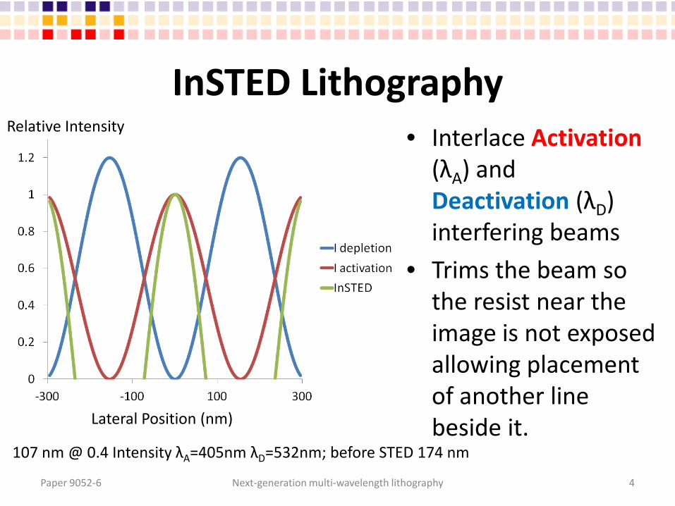
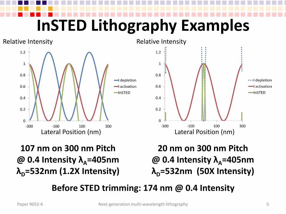
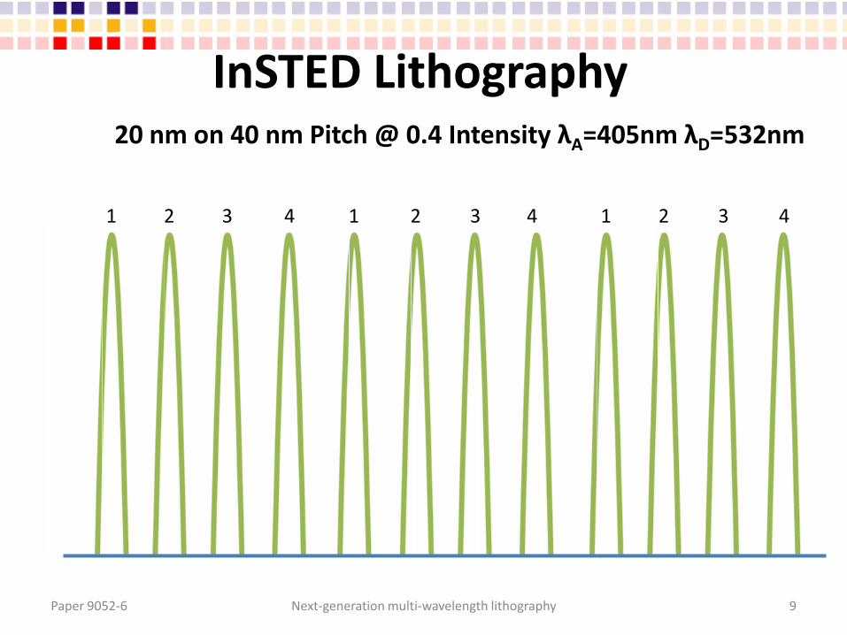
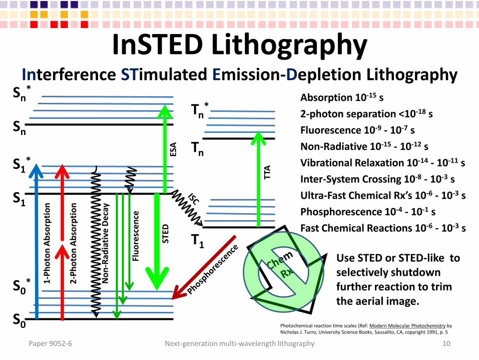
InSTED Lithography • Interlace Activation
(λA) and Deactivation (λD) interfering beams
• Trims the beam so the resist near the image is not exposed allowing placement of another line beside it.
107 nm @ 0.4 Intensity λA=405nm λD=532nm; before STED 174 nm
Paper 9052-6 Next-generation multi-wavelength lithography 4
Use STED or STED-like to selectively shutdown further reaction to trim the aerial image.
Photochemical reaction time scales (Ref: Modern Molecular Photochemistry by Nicholas J. Turro, University Science Books, Sausalito, CA, copyright 1991, p. 5
Paper 9052-6 Next-generation multi-wavelength lithography 10
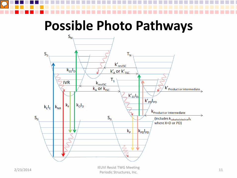
Possible Photo Pathways
2/23/2014 IEUVI Resist TWG Meeting
Periodic Structures, Inc. 11
Presenter
Presentation Notes
Photophysical schemes for multi-color photolithography. The photosensitizer begins in its electronic ground state S0, and is promoted to its first excited electronic state, S1, via absorption (blue arrow). The electronically-excited molecule relaxes to its ground vibrational state via intramolecular vibrational redistribution (IVR). The molecule can then activate a reaction, relax nonradiatively, fluoresces, undergo stimulated emission, or transfer to its triplet via intersystem-crossing. It can also be driven to a higher electronic state Sn by the deactivation beam. If ISC occurs it moves to the triplet state where analogous paths exist with the addition of reverse and phosphorescence and stimulated phosphorescence, triplet EEA by absorbing ID, or by absorbing the phosphorescence deactivation beam. In the triplet it can move on to react or form intermediate excited state compounds that may form diffusion limited solvated electrons.
Spectra and Excitation-Depletion Absorbance
Fluorescence
Phosphorescence
STED 2-Photon
1-Photon
Rela
tive
Spe
ctra
l Uni
ts
Wavelength (nm) 300 810 532 400
12 Paper 9052-6 Next-generation multi-wavelength lithography 12
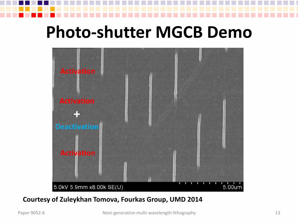
Photo-shutter MGCB Demo
Courtesy of Zuleykhan Tomova, Fourkas Group, UMD 2014
Activation
+ Deactivation
Activation
Activation
Paper 9052-6 Next-generation multi-wavelength lithography 13
Thin Resist Result
NA=1.45 Resolution Pitch Limit: 673-551 nm Achieved 400 nm w/pattern collapse Fourkas Group Set up
Paper 9052-6 Next-generation multi-wavelength lithography 14
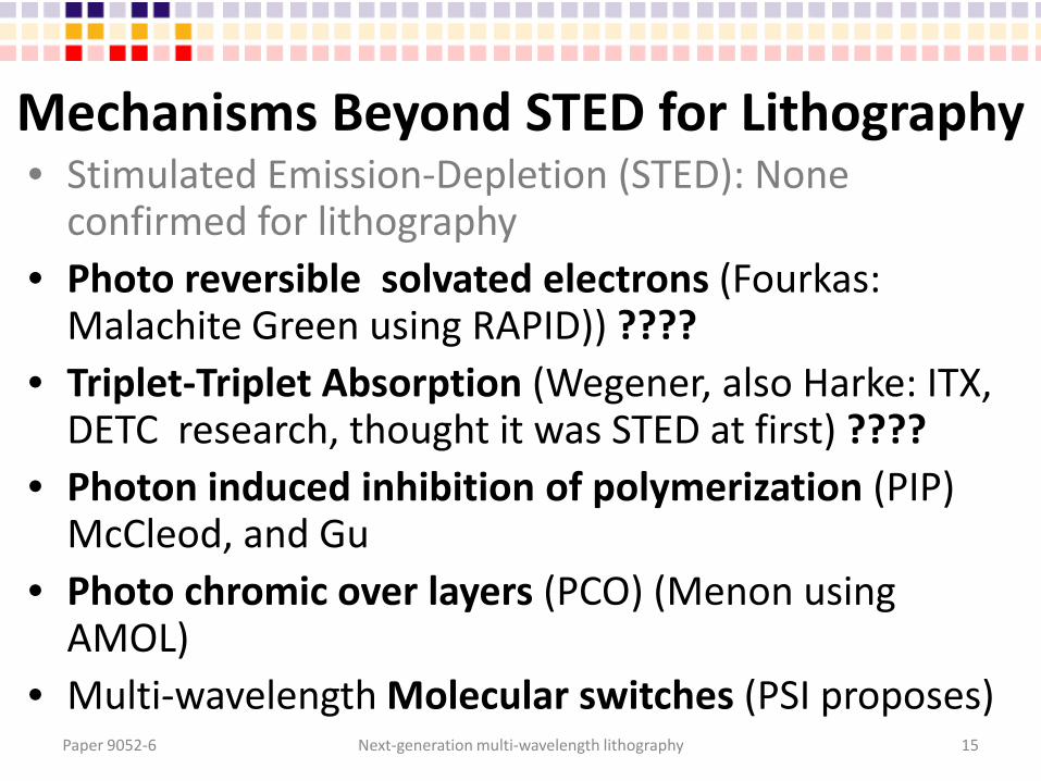
Mechanisms Beyond STED for Lithography • Stimulated Emission-Depletion (STED): None
confirmed for lithography • Photo reversible solvated electrons (Fourkas:
Malachite Green using RAPID)) ???? • Triplet-Triplet Absorption (Wegener, also Harke: ITX,
DETC research, thought it was STED at first) ???? • Photon induced inhibition of polymerization (PIP)
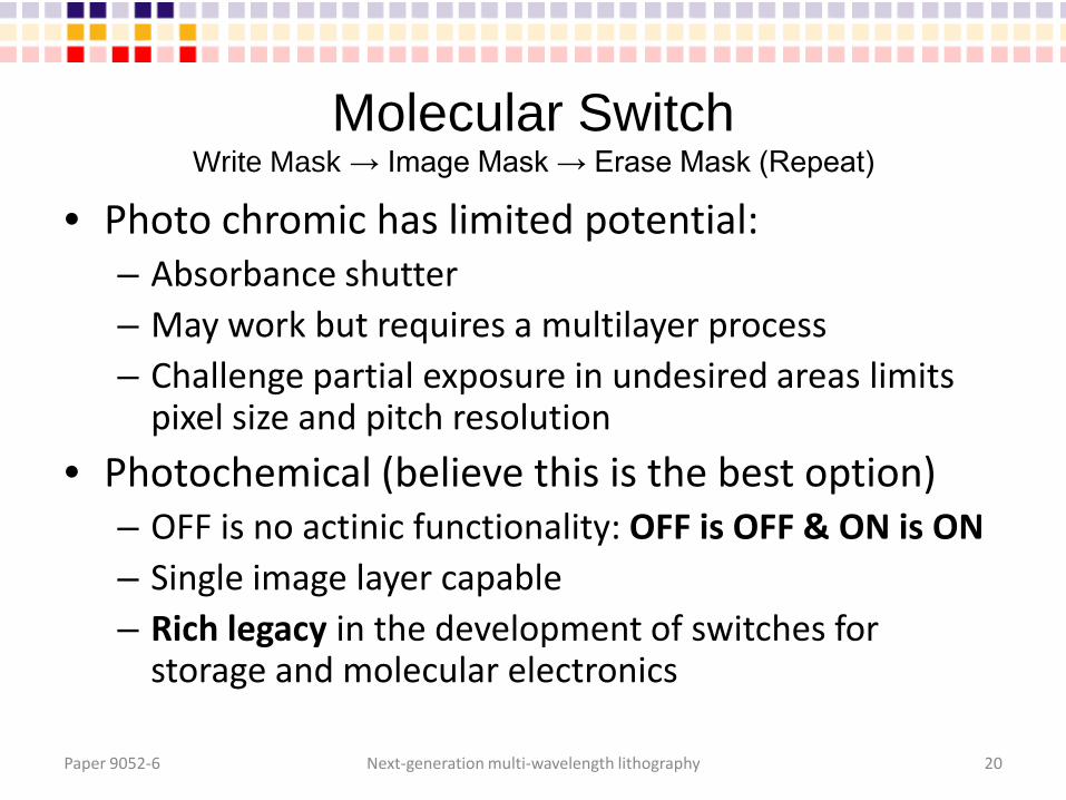
McCleod, and Gu • Photo chromic over layers (PCO) (Menon using
• Photo chromic has limited potential: – Absorbance shutter – May work but requires a multilayer process – Challenge partial exposure in undesired areas limits
pixel size and pitch resolution
• Photochemical (believe this is the best option) – OFF is no actinic functionality: OFF is OFF & ON is ON – Single image layer capable – Rich legacy in the development of switches for
storage and molecular electronics
Paper 9052-6 Next-generation multi-wavelength lithography 20
Super-resolution Lithography System Schematic
Camera
Telecentric Relay
DMD B B R
Beam-splitter
Objective
Light Pipe
Frustrated Prism
Dose Detector
Stage
Grating Phase Shifter
Laser Diodes
Inhibition Laser
Paper 9052-6 Next-generation multi-wavelength lithography 21
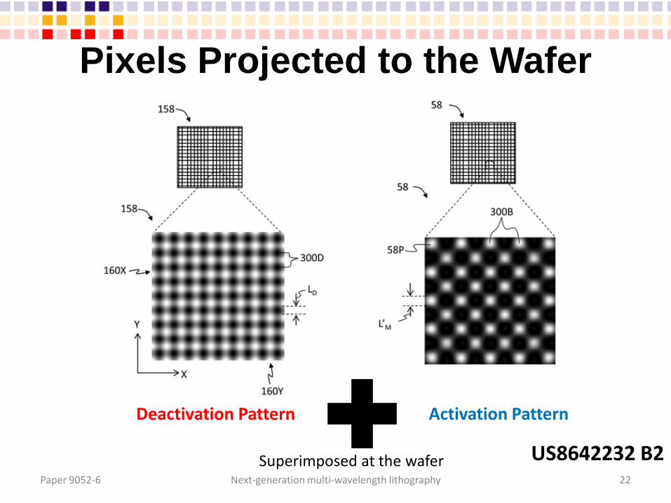
US8642232 B2
Pixels Projected to the Wafer
Paper 9052-6 Next-generation multi-wavelength lithography 22
US8642232 B2
Deactivation Pattern Activation Pattern
Superimposed at the wafer
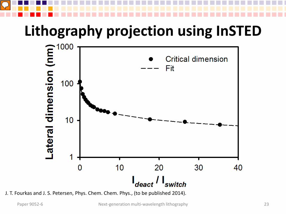
Lithography projection using InSTED
J. T. Fourkas and J. S. Petersen, Phys. Chem. Chem. Phys., (to be published 2014).
Paper 9052-6 Next-generation multi-wavelength lithography 23
Presenter
Presentation Notes
Fig. 4 Lithography projection of the imaging capability of a tool using 2-color interference. (a) The critical dimension for images with a NILS of 1.5 or slightly larger relative to the ratio of the depletion intensity to the switch intensity. (b) NILS for 2-color interference lithography as a function of critical dimension for different deactivation intensities. The images were formed using two-beam interference of a 532-nm deactivation source with an effective NA of 0.9 and a blanket exposure of a 405-nm excitation source. The pitch for each individual exposure is 295.556 nm.
Throughput varies with the type of Pattern and the Line Edge Resolution
Pattern Type
Continuous Lines
Broken Lines
Arbitrary Pattern
Assumptions: 2560 by 1600 pixel DMD 20 kHz frame rate, 7.8 μm DMD pixel spacing 20 nm image pixel 50 mm by 75 mm footprint, 0.5 m/s maximum scan rate 266 nm interference wavelength 0.95 NA Period = λ/2NA = 140 nm Magnification = 7.8/.14 = 55.7 Acceleration = 1g
Paper 9052-6 Next-generation multi-wavelength lithography 24
Line Edge Placement
Time/Footprint
20 nm 35.3 s (102/hr)
117.5 s (30.6/hr) 20 nm
2.5 nm 460.2 s (7.82/hr)
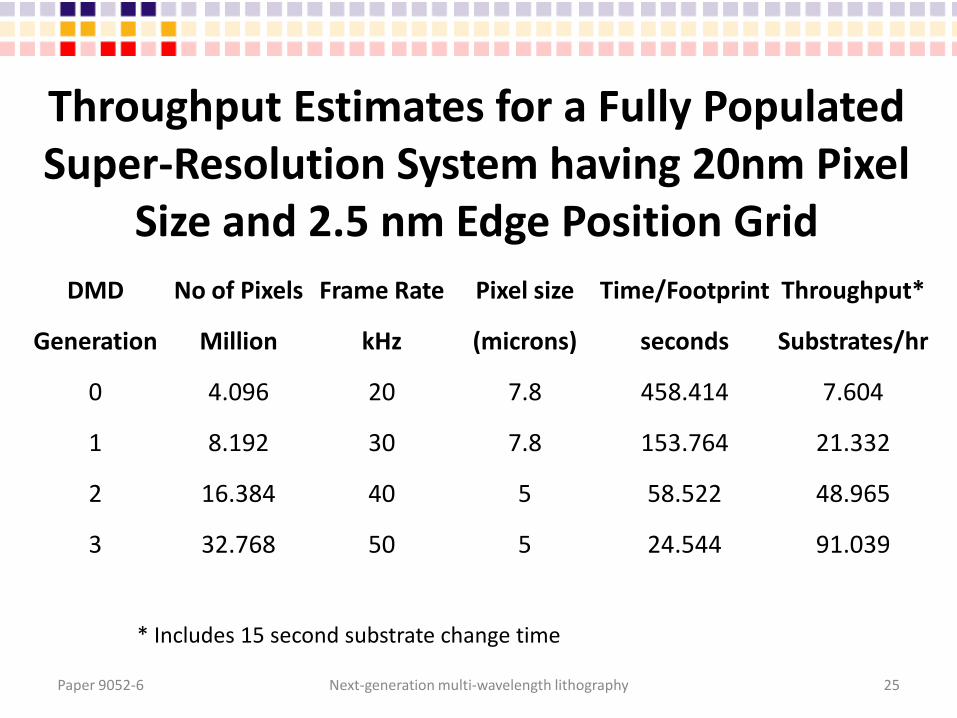
Throughput Estimates for a Fully Populated Super-Resolution System having 20nm Pixel
Size and 2.5 nm Edge Position Grid DMD No of Pixels Frame Rate Pixel size Time/Footprint Throughput*
Generation Million kHz (microns) seconds Substrates/hr
0 4.096 20 7.8 458.414 7.604
1 8.192 30 7.8 153.764 21.332
2 16.384 40 5 58.522 48.965
3 32.768 50 5 24.544 91.039
* Includes 15 second substrate change time
Paper 9052-6 Next-generation multi-wavelength lithography 25
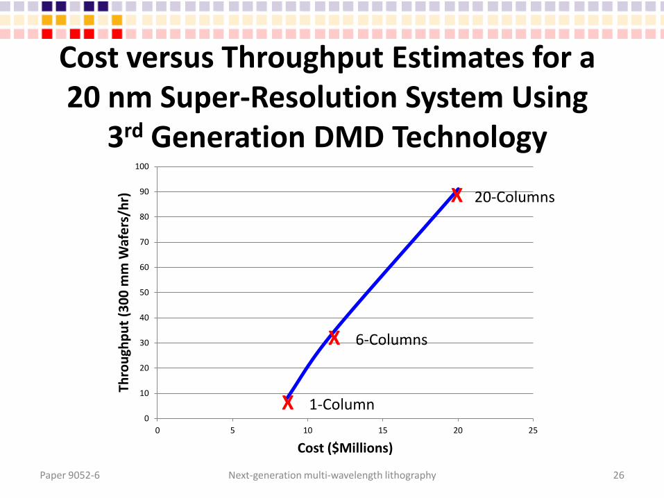
Cost versus Throughput Estimates for a 20 nm Super-Resolution System Using
3rd Generation DMD Technology
0
10
20
30
40
50
60
70
80
90
100
0 5 10 15 20 25
Thro
ughp
ut (3
00 m
m W
afer
s/hr
)
Cost ($Millions)
X 1-Column
X 6-Columns
X 20-Columns
Paper 9052-6 Next-generation multi-wavelength lithography 26
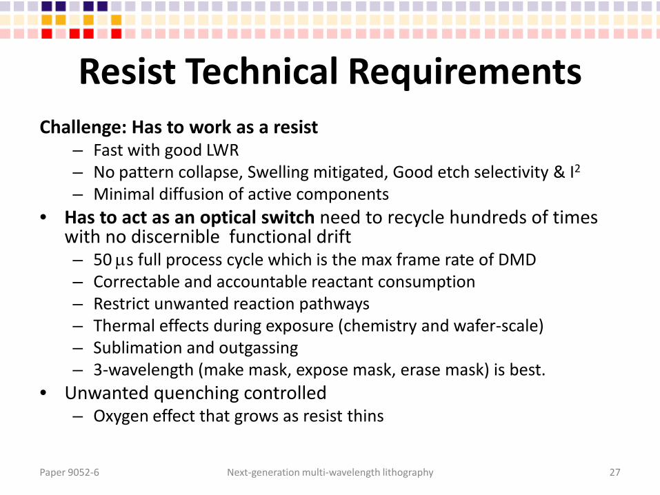
Resist Technical Requirements Challenge: Has to work as a resist
– Fast with good LWR – No pattern collapse, Swelling mitigated, Good etch selectivity & I2 – Minimal diffusion of active components
• Has to act as an optical switch need to recycle hundreds of times with no discernible functional drift – 50 µs full process cycle which is the max frame rate of DMD – Correctable and accountable reactant consumption – Restrict unwanted reaction pathways – Thermal effects during exposure (chemistry and wafer-scale) – Sublimation and outgassing – 3-wavelength (make mask, expose mask, erase mask) is best.
• Unwanted quenching controlled – Oxygen effect that grows as resist thins
Paper 9052-6 Next-generation multi-wavelength lithography 27
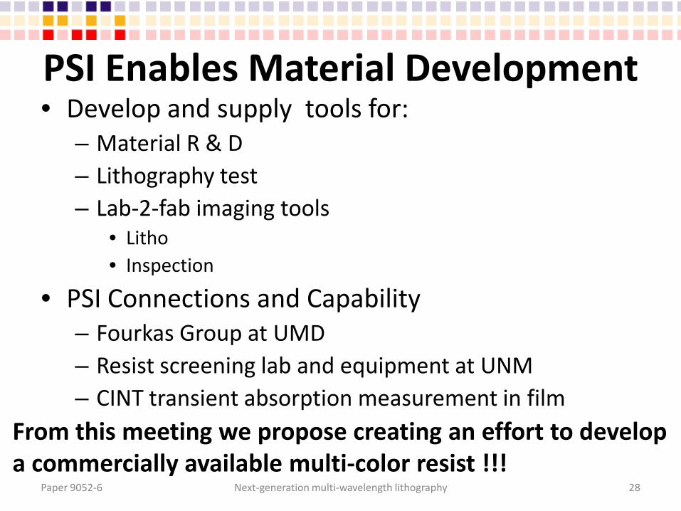
PSI Enables Material Development • Develop and supply tools for:
– Material R & D – Lithography test – Lab-2-fab imaging tools
• Litho • Inspection
• PSI Connections and Capability – Fourkas Group at UMD – Resist screening lab and equipment at UNM – CINT transient absorption measurement in film
From this meeting we propose creating an effort to develop a commercially available multi-color resist !!!
Paper 9052-6 Next-generation multi-wavelength lithography 28
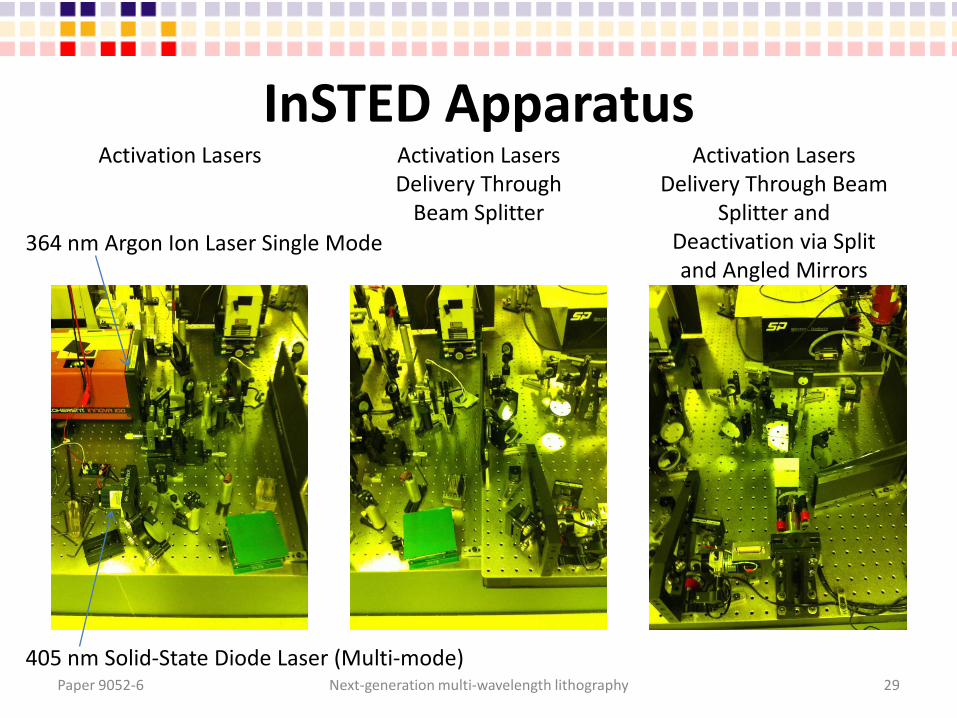
InSTED Apparatus Activation Lasers Delivery Through
Beam Splitter
Activation Lasers Activation Lasers Delivery Through Beam
Splitter and Deactivation via Split and Angled Mirrors
405 nm Solid-State Diode Laser (Multi-mode)
364 nm Argon Ion Laser Single Mode
Paper 9052-6 Next-generation multi-wavelength lithography 29
Thank You Work supported by NSF Grant: IIP-1318211
0
0.2
0.4
0.6
0.8
1
1.2
-0.4 -0.3 -0.2 -0.1 0 0.1 0.2 0.3 0.4
Expo
sure
Dos
e
Image Position (Microns)
Exposure Dose Profile for Various Inhibition to Exposure Intensity Ratios
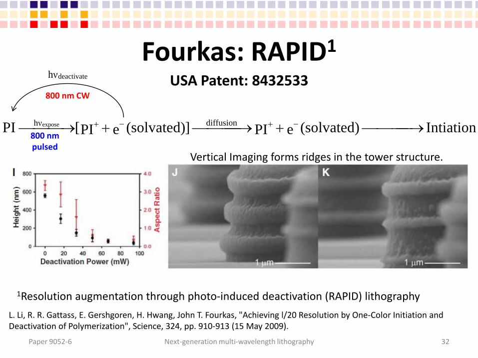
1Resolution augmentation through photo-induced deactivation (RAPID) lithography
L. Li, R. R. Gattass, E. Gershgoren, H. Hwang, John T. Fourkas, "Achieving l/20 Resolution by One-Color Initiation and Deactivation of Polymerization", Science, 324, pp. 910-913 (15 May 2009).
Vertical Imaging forms ridges in the tower structure.
USA Patent: 8432533
Paper 9052-6 Next-generation multi-wavelength lithography 32
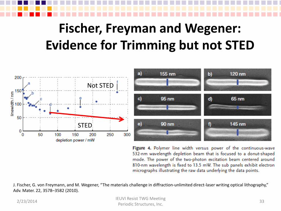
J. Fischer, G. von Freymann, and M. Wegener, “The materials challenge in diffraction-unlimited direct-laser writing optical lithography,” Adv. Mater. 22, 3578–3582 (2010).
Fischer, Freyman and Wegener: Evidence for Trimming but not STED
Z. Gan, Y. Cao, R. A. Evans and M. Gu, Nat. Commun., 2013, 4, 2061
Paper 9052-6 Next-generation multi-wavelength lithography 34
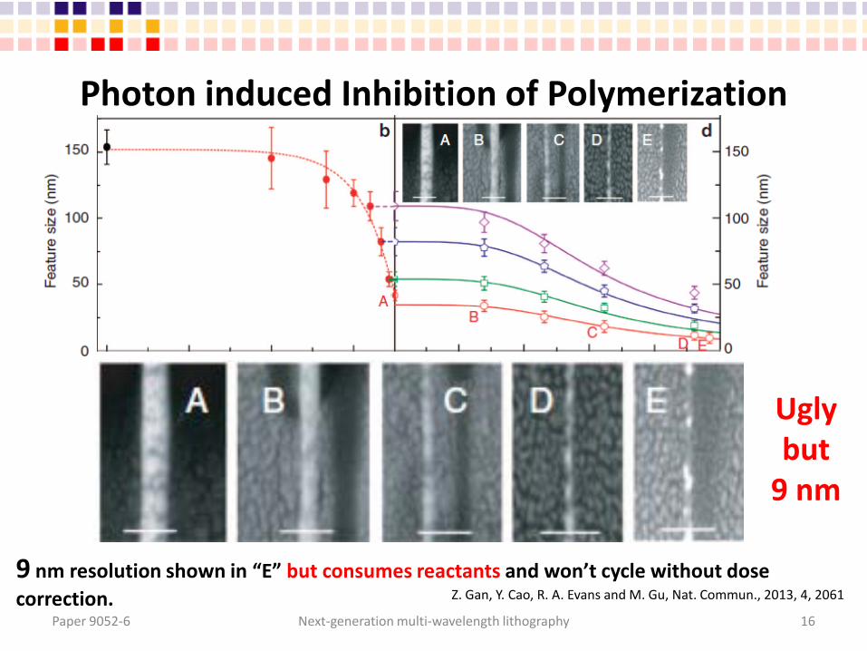
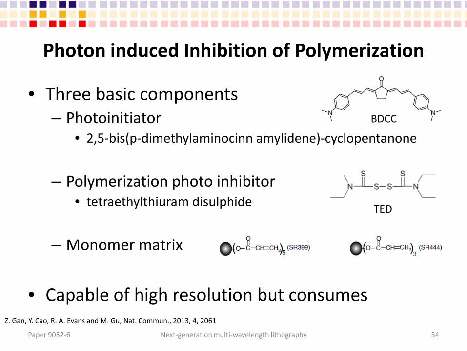
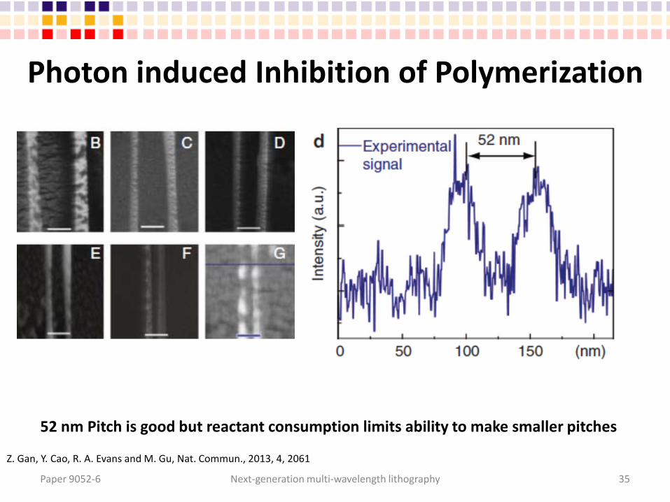
Photon induced Inhibition of Polymerization
Z. Gan, Y. Cao, R. A. Evans and M. Gu, Nat. Commun., 2013, 4, 2061
52 nm Pitch is good but reactant consumption limits ability to make smaller pitches
Paper 9052-6 Next-generation multi-wavelength lithography 35
Menon: AMOL
R. Menon, H-Y Tsai and S. W. Thomas III, "Far-Field Generation of Localized Light Fields using Absorbance Modulation", PRL 98, 043905 (2007).
Control
Paper 9052-6 Next-generation multi-wavelength lithography 36
References
• S. W. Hell and J. Wichmann, Opt. Lett., 1994, 19, 780-782. • J. T. Fourkas and J. S. Petersen, Phys. Chem. Chem. Phys., (to be published 2014). • K. Berggren, A. Bard, J. Wilbur, J. Gillaspy, A. Helg, J. McClelland, S. Rolston, W. Phillips, M. Prentiss and G.
Whitesides, Science, 1995, 269, 1255-1257. • L. J. Li, R. R. Gattass, E. Gershgoren, H. Hwang and J. T. Fourkas, Science, 2009, 324, 910-913. • T. F. Scott, B. A. Kowalski, A. C. Sullivan, C. N. Bowman and R. R. McLeod, Science, 2009, 324, 913-917. • T. L. Andrew, H. Y. Tsai and R. Menon, Science, 2009, 324, 917-921. • J. T. Fourkas, J. Phys. Chem. Lett., 2010, 1, 1221-1227. • J. Fischer, G. von Freymann and M. Wegener, Adv. Mater., 2010, 22, 3578-3582. • J. Fischer and M. Wegener, Opt. Mater. Expr., 2011, 1, 614-624. • B. Harke, P. Bianchini, F. Brandi and A. Diaspro, Chemphyschem, 2012, 13, 1429-1434. • B. Harke, W. Dallari, G. Grancini, D. Fazzi, F. Brandi, A. Petrozza and A. Diaspro, Adv. Mater., 2013, 25, 904-909. • J. Fischer and M. Wegener, Laser Photon. Rev., 2013, 7, 22-44. • M. P. Stocker, L. Li, R. R. Gattass and J. T. Fourkas, Nat. Chem., 2011, 3, 223-227. • Y. Y. Cao, Z. S. Gan, B. H. Jia, R. A. Evans and M. Gu, Opt. Expr., 2011, 19, 19486-19494. • Z. Gan, Y. Cao, R. A. Evans and M. Gu, Nat. Commun., 2013, 4, 2061. • Z. S. Gan, Y. Y. Cao, B. H. Jia and M. Gu, Opt. Expr., 2012, 20, 16871-16879
Paper 9052-6 Next-generation multi-wavelength lithography 37