INTERNATIONAL TECHNOLOGY ROADMAP FOR SEMICONDUCTORS 2.0 2015 EDITION INTERCONNECT THE ITRS 2.0 IS DEVISED AND INTENDED FOR TECHNOLOGY ASSESSMENT ONLY AND IS WITHOUT REGARD TO ANY COMMERCIAL CONSIDERATIONS PERTAINING TO INDIVIDUAL PRODUCTS OR EQUIPMENT. THE INTERNATIONAL TECHNOLOGY ROADMAP FOR SEMICONDUCTORS 2.0: 2015
Transcript
INTERNATIONAL TECHNOLOGY ROADMAP
FOR SEMICONDUCTORS 2.0
2015 EDITION
INTERCONNECT
THE ITRS 2.0 IS DEVISED AND INTENDED FOR TECHNOLOGY ASSESSMENT ONLY AND IS WITHOUT REGARD TO
ANY COMMERCIAL CONSIDERATIONS PERTAINING TO INDIVIDUAL PRODUCTS OR EQUIPMENT.
THE INTERNATIONAL TECHNOLOGY ROADMAP FOR SEMICONDUCTORS 2.0: 2015
THE INTERNATIONAL TECHNOLOGY ROADMAP FOR SEMICONDUCTORS 2.0: 2015
Table of Content Interconnect........................................................................................................................... 1
Figure INTC4 Schematic Representation of the Various Key Process Modules and 3D-stacking
Options when using Through-Si-Via 3D-SIC Technologies .................................10
Figure INTC5 Schematic Representation of the Various Key Process Modules and 3D-stacking
Options when using Through-Si-Via 3D-WLP Technologies ...............................11
Figure INTC6 Evolution of Jmax (from device requirement) and JEM (from targeted lifetime) ..14 Figure INTC7 Comparison of the Lifetime Improvement versus the Resistivity Increase for
Different EM Resistance Booster Technologies11 ..............................................14
Figure INTC17 Schematic Cross-sections of the Challenges for Si-TSV Plasma Etching...........38
Figure INTC18 Cu and W-based TSV Options as a Function of TSV Diameter and Aspect Ratio, in Accordance with the 3D Interconnect Hierarchy and Roadmap ......................40
List of Tables Table INTC1 2015 Interconnect Difficult Challenges ..................................................................3
Table INTC9 Advantages and Concerns for Cu Extensions, Replacements and Native Device Interconnects .......................................................................................................43
Interconnect 1
INTERCONNECT
1. SCOPE The Interconnect chapter of the ITRS 2.0 addresses the wiring system that distributes clock and other signals to the various functional blocks of a CMOS integrated circuit, along with providing necessary power and ground connections. The process scope begins at the contact level with the pre-metal dielectric and continues up to the wirebond pads, describing deposition, etch and planarization steps, along with any necessary etches, strips and cleans. A section on reliability and performance includes specifications for electromigration and calculations of delay. The process scope of 3D integration is described from both process and architectural point of view.
1.1. INTRODUCTION The Interconnect chapter of the 1994 National Technology Roadmap for Semiconductors (NTRS) described the first needs for new conductor and dielectric materials that would be necessary to meet the projected overall technology requirements. With the publication of the 1997 edition of the NTRS, the introduction of copper-containing chips was imminent. The 1999 International Roadmap for Semiconductors (ITRS) emphasized an ongoing change to new materials that were being introduced at an unprecedented pace. The 2001 ITRS described continued new materials introductions and highlighted the problem of increases in conductor resistivity as linewidths approach electron mean free paths. The slower than projected pace of low-κ dielectric introduction for microprocessors (MPUs) and application-specific ICs (ASICs) was one of the central issues for the 2003 ITRS Interconnect area. The 2005 ITRS showed the calculated electron scattering induced Cu resistivity rise for future technology generations, as well as the resultant effect on resistance and capacitance (RC) performance metrics. A crosstalk metric was also introduced in 2007. Managing the rapid rate of materials introduction and the concomitant complexity represents the overall near-term challenge. For the long term, material innovation with traditional scaling will no longer satisfy performance requirements. Interconnect innovation with optical, radio frequency (RF), or vertical integration combined with accelerated efforts in design and packaging will deliver the continuing ability to match the performance scaling expected with Moore’s Law.
The function of the interconnect or wiring system is to distribute clock and other signals and to provide power/ground, to and among, the various circuit/system functions on a chip. The fundamental development requirement for interconnect is to meet the high-bandwidth low-power signaling needs without introducing performance bottlenecks as scaling continues.
Although copper-containing chips were introduced in 1998 with silicon dioxide insulators, reduction of the insulator dielectric constant indicated by the ITRS has been problematic. Fluorine doped silicon dioxide (κ = 3.7) was introduced at 180 nm, however insulating materials with κ = 2.7–3.0 were not widely used until 90 nm. The reliability and yield issues associated with integration of these materials with dual damascene copper processing proved to be more challenging than expected. The integration of porous low-κ materials is expected to be even more challenging. Since the development and integration of these new low-κ materials is rather time invariant, the anticipated acceleration of the MPU product cycle (two versus three years until 2009) will shift the achievable κ to later technology generations. The various dielectric materials that are projected to comprise the integrated dual damascene dielectric stack for all years of the roadmap and the complimentary materials when integrating with porous low-κ dielectrics are depicted in the Dielectric Potential Solutions Figure, INTC 10.
1.2. WHAT’S NEW FOR 2015? Overall simplified from 2013 style focusing on roadmap related issues The Technology Requirements Table (INTC2) has been substantially changed from 2013 style reorganized as
o Roadmap only for levels with minimum pitches presented o General requirements – e.g., bulk resistivity and dielectric constant o Level specific requirements determined by the nature of the wire geometry – e.g., barrier thickness and
effective resistiv y it Low-κ roadmap – substantially changed due to delay of the introduction of new materials and the continuous
usage of non-porous low-κ materials o New range for bulk κ o Air gaps expected to be a possible solution for κ bulk < 2.0 o Evaluation of new parametric indicator considering sidewall damage by RIE or wet cleaning
Renewal of metallization potential solution with appropriate material candidates and their promising application.
THE INTERNATIONAL TECHNOLOGY ROADMAP FOR SEMICONDUCTORS 2.0: 2015
2 Interconnect
o Barriers (< 3.0 nm) and nucleation layers are a critical challenge o Approaches of new liners (Co, Ru and others) stacked with barrier layers are proliferating o Capping metal for reliability improvement nearing production o Reconsideration of appropriate material candidates with their potential duration as MnSiO, CuAl and
CuTi. o Consideration of alternative materials with weaker size effect as W, Mo, Ru and NiSi.
Revised 3D TSV roadmap tables Revised process modules roadmap tables
2. SUMMARY For 2015, interconnect performance is at the forefront as a key challenge to achieve overall chip performance. Low-κ scaling (κ < 2.55) was greatly slowed down due κ-value increase by plasma and mechanical damages induced during interconnect integration. Air gap structures are now considered a mainstream potential solution for the ILD, recognizing their increased maturity. Air gap structure with SiO2 ILD has introduced into NAND Flash memory to reduce the word-line capacitance. Recently in MPU, air gap structure with SiOC ILD has also introduced to reduce the line-to-line capacitance. The ITRS team firmly believes that any substantial reduction in effective κ will not be achieved by further materials improvements of porous ultra-low-κ (κ ≤ 2) but by the use of low-κ scaled diffusion barriers and air gap structures. For low-κ, this is the end of materials solutions and the beginning of architecture solutions. Delays in the emergence of quality ALD processes prevent the deposition of the required sub-2 nm barriers, and are a top concern. Discussions on 3D interconnects have been moved out of the emerging interconnect section, with TSVs starting production.
2.1. DIFFICULT CHALLENGES Table INTC1 highlights the five key challenges in the long term (< 12 nm [Mx hp]). The most difficult challenge for interconnects is the impact of size effects on interconnect structures must be mitigated.
Future effective κ requirements preclude the use of a trench etch stop for dual damascene structures. Dimensional control is a key challenge for present and future interconnect technology generations and the resulting difficult challenge for etch is to form precise trench and via structures in low-κ dielectric material to reduce variability in RC. The dominant architecture, damascene, requires tight control of pattern, etch and planarization. To extract maximum performance, interconnect structures cannot tolerate variability in profiles without producing undesirable RC degradation. These dimensional control requirements place new demands on high throughput imaging metrology for measurement of high aspect ratio structures. New metrology techniques are also needed for in-line monitoring of adhesion and defects. Larger wafers and the need to limit test wafers will drive the adoption of more in situ process control techniques. Dimensional control, a challenge now, will become even more critical as new materials, such as porous low-κ dielectrics and ALD metals, play a role at the tighter pitches and higher aspect ratios (A/R) of intermediate and global levels.
THE INTERNATIONAL TECHNOLOGY ROADMAP FOR SEMICONDUCTORS 2.0: 2015
Five Most Critical Challenges < 12 nm [Mx hp] Summary of Issues
Materials
Mitigate impact of size effects in interconnect structures
Line and via sidewall roughness, intersection of porous low-κ voids with sidewall, barrier roughness, and copper surface roughness will all adversely affect electron scattering in copper lines and cause increases in resistivity.
Metrology
Three-dimensional control of interconnect features (with its associated metrology) will be required
Line edge roughness, trench depth and profile, via shape, etch bias, thinning due to cleaning, CMP effects. The multiplicity of levels, combined with new materials, reduced feature size and pattern dependent processes, use of alternative memories, optical and RF interconnect, continues to challenge.
Process
Patterning, cleaning, and filling at nano dimensions
As features shrink, etching, cleaning, and filling high aspect ratio structures will be challenging, especially for low-κ dual damascene metal structures and DRAM at nano-dimensions.
Complexity in Integration
Integration of new processes and structures, including interconnects for emerging devices
Combinations of materials and processes used to fabricate new structures create integration complexity. The increased number of levels exacerbate thermomechanical effects. Novel/active devices may be incorporated into the interconnect.
Practical Approach for 3D
Identify solutions which address 3D interconnect structures and other packaging issues
Three-dimensional chip stacking circumvents the deficiencies of traditional interconnect scaling by providing enhanced functional diversity. Engineering manufacturable solutions that meet cost targets for this technology is a key interconnect challenge.
2.2. INTERCONNECT ARCHITECTURES
2.2.1. INTRODUCTION Two specific classes of products: Logic (MPUs and SoCs) and NAND flash memory are discussed. Figure INTC1 shows a typical cross-section of hierarchical scaling for an MPU device (left), SoC (middle) and Flash memory device (right).
Dielectric Capping
LayerCopper
Conductor with
Barrier / Nucleation
Layer
Pre-Metal Dielectric
Tungsten Contact
Plug
Inter-Mediate(=M1x1)
Inter-Mediate(=M1x1)
Metal 1Metal 1
Passivation
DielectricEtch Stop Layer
Semi-Global (=M1x2)
Semi-Global (=M1x2)
Metal 1 Pitch
Via
Wire
Metal 1 Pitch
Via
Wire
Via
Wire
Via
Wire
Metal 1 Pitch
Via
Wire
Via
Wire
Metal 1 Pitch
Global(=IMx1.5~2µm)
Global(=IMx1.5~2µm)
Inter-Mediate(=M1x1)
Inter-Mediate(=M1x1)
Metal 1Metal 1
Global(=IMx1.5~2µm)
Global(=IMx1.5~2µm) Metal 3
Metal 0Metal 1
Metal 2
Poly Pitch
Metal 1 Pitch
Metal 3
Metal 0Metal 1
Metal 2
Poly Pitch
Metal 1 Pitch
Figure INTC1 Typical Cross-sections of Hierarchical Scaling (MPU Device (left), SoC (middle) and Flash Memory (right))
2.2.2. LOGIC (MPU/SOC) MPUs utilize a high number of metal layers with a hierarchical wiring approach of steadily increasing pitch and thickness at each conductor level to alleviate the impact of interconnect delay on performance. To accommodate the need for
THE INTERNATIONAL TECHNOLOGY ROADMAP FOR SEMICONDUCTORS 2.0: 2015
4 Interconnect
ground planes or on-chip decoupling capacitors, the growth of metal levels is projected to increase beyond those specified, solely to meet performance requirements. SoCs share many of the technology attributes of MPUs, for example, Cu wiring and low-κ dielectrics. SoC design methodology is generally more regular, consisting of M1, intermediate, semi-global (2X intermediate) and global (4X intermediate) wire pitches.
The accelerated scaling of MPU pitch has aggravated the copper electromigration problem. Jmax limits for current dielectric cap technologies for copper will be exceeded by 2017. Modification of the Cu surface to form CuSiN or use of alloys such as Cu-Al can yield significant electromigration improvements. Implementation of a selective metal cap technology for copper, such as CoWP, will result in even higher electromigration capability. However, there is still concern about yield loss due to metal shorts caused by these selective processes. Improved dielectric caps are also being explored.
Damascene process flows dominate MPU/SoC fabrication methodologies. Figure INTC2 illustrates two typical inter-level dielectric (ILD) architectures used in the creation of interconnect wiring levels. Types of dielectric structures have been reduced from three to two (Inorganic/Organic hybrid structure has been removed). While current copper damascene processes utilize PVD Ta-based barriers and Cu nucleation layers, continued scaling of feature size requires development of other materials and nucleation layer deposition solutions. Continuous improvement of tools and chemistries will extend electrochemically deposited (ECD) Cu to the end of the forecasted roadmap but small, high A/R features necessitate the simultaneous development and subsequent selection of alternative filling techniques. A thin barrier is also needed to maintain the effective conductor resistivity in these features. Nucleation layer conformity requirements become more stringent to enable Cu ECD filling of damascene features. Surface segregated, CVD, ALD, and dielectric barriers represent intermediate potential solutions; zero thickness barriers are desirable but not required.
Accordingly, numbers of Cu resistivity for minimum M1, intermediate and global wires are now listed for all the years of the roadmap. The effect of this resistivity increase on the RC performance metrics is also calculated and included in the technology requirements table. The total variability of M1 wire resistance due to CD variation and scattering has been calculated and is also included in the MPU technology requirements table. Since the length of Metal 1 and intermediate wires usually shrinks with traditional scaling, the impact of their delay on performance is minor. Global interconnects, which have the greatest wire lengths, will be impacted most by the degraded delay. The benefit of materials changes or some amelioration of the Cu resistivity rise will be insufficient to meet overall performance requirements. The trend toward multi-core MPU design has alleviated some of the delay issues associated with ever increasing lengths of global interconnects
Although introduction of air-gap structures into Cu interconnects has been realized in MPU, it is still a significant challenge. Several integration schemes and structures for air-gap formation have been reported. They can be classified into two categories according to whether gap formation is performed before or after the upper metal formation.
Figure INTC2 Typical ILD Architectures
THE INTERNATIONAL TECHNOLOGY ROADMAP FOR SEMICONDUCTORS 2.0: 2015
Interconnect 5
2.2.3. MEMORY (FLASH) Flash memory utilizes a simple hierarchical wiring with three or four metal layers. Bit-line (metal 1 layer) in flash memory reflects the most aggressive metal pitch, and its contact layer has the highest aspect ratio in all semiconductor devices. Therefore, they face the largest RC delay due to the size effect and the challenges on patterning and metal fill. Metal 2 layer and beyond utilize relaxed metal pitch.
As well as in logic device, process flows dominate flash memory fabrication methodologies. Copper damascene processes utilize PVD-based barriers and Cu nucleation layers and continued scaling of feature size requires development of other materials and nucleation layer deposition solutions. Technology requirements for metallization are listed in logic section above in detail. As a new trend, tungsten as the finest Bit-line interconnects material has been introduced for its advantage on metallization process, airgap formation and electromigration resistance. However it requires a design to deal with higher bulk resistivity than copper.
Electron scattering models have been improved and can now predict the Cu resistivity rise as a function of linewidth and aspect ratio. There is a significant contribution to the increase in resistivity by the electron scattering at both grain boundaries and interfaces. To date, research has not identified any potential solutions to this problem. Three-dimensional control of critical dimension (3DCD) interconnect features has been listed as one of the critical challenges in several editions of the ITRS.
Air-gap structure has been adapted ahead to other devices with the combination of tungsten interconnects. Formation of air-gap by plasma-CVD dielectric deposition into space between reactive ion-etched tungsten interconnects is a most promising solution. In copper damascene interconnects, introducing air-gap structure will still be challenging as well as in logic device. Usage of low-κ materials in Bit-line can be effective to reduce capacitance; however, they need to have dielectric film properties to endure high voltage operations which are unique in flash memory.
2.2.4. MORE THAN MOORE Minimum feature size M1 and intermediate Cu wiring, in MPUs and SOCs, has already experienced a exponential increase in resistivity in scaling technology nodes due to electron scattering [9-11]. In additional, there is a more than projected decrease Cu cross sectional area with scaling due to the non-scaling on barrier metal thickness. These parameters combine to form to a larger than expected Cu resistance increase which is only partially mitigated by the decrease in line length with scaling. Global wiring levels, with their much larger linewidths, will be the last to be impacted by size effects in Cu. The resistivity of the smallest pitch global wiring level is expected to increase by more than double by the end of this decade. For some applications, this global wiring starts at the next Cu wiring level after M1. These global wires traverse long wiring lengths and increased resistivity can negatively impact performance. Cu interfaces, microstructures, and impurity levels will need to be engineered to alleviate the impact of this resistivity rise. MPUs use a hierarchical wiring approach in which the pitch and thickness of the global wires are increased at each level. Indeed, the final global wiring level is little changed from one generation to the next and so will not be affected by electron scattering effects. In the 2013 table, the global wiring pitch will be estimated to be constant because significant changes are not expected.
Other design alternatives are the use of repeaters or oversized drivers, both of which impact chip size and power. The most likely near-term solution is the use of very high density TSVs as an enabling technology for three-dimensional chip stacking. This technology can reduce overall interconnect wire lengths while allowing incorporation of non-Si solutions for improved functional diversity. The other near-term solutions are judicious use of design and signaling options and packaging to minimize the effect of the narrower more resistive global wires. A great deal of research is underway on the use of either RF or optical techniques to resolve this issue. More radical solutions include superconductors, carbon nanotubes, etc. A full discussion of 3D IC, a proposed roadmap for high density TSV and other alternatives is contained in a TSV related section.
The use of optical signals for on-die interconnects has been an active research topic for many years. Integration of optics on-die has also been proposed to increase off chip BW densities. To date it appears that for on-die interconnects, electrical versions will be sufficient to meet roadmap needs through the 8nm technology node [20]. In this comparison of on-die electrical (RC and transmission line) vs optics (off-die and on-die lasers), the study indicates that while optical interconnects can potentially provide a higher BW density, power will be higher and furthermore that electrical interconnects are sufficient through the 8nm node. While some of the assumptions in this study are overly optimistic, the relative assessments appear reasonable. In addition, it should be noted that only power per bit and BW density are
THE INTERNATIONAL TECHNOLOGY ROADMAP FOR SEMICONDUCTORS 2.0: 2015
6 Interconnect
compared. The integration of optics onto a leading edge CMOS node based CPU or switch chip will not only increase the processing cost but will introduce many additional avenues for yield loss. Lasers are typically temperature sensitive as well, hindering inclusion on-die, and circumvented this issue by locating off-die lasers adds additional packaging cost and coupling loss (power).
For stand-alone optical transceivers, CMOS-compatible optical interconnect transceivers continue to make progress however, as Si Photonics based optical interconnect modules enter the market for data center and telecommunications links. One can envision that out beyond the 8nm node there is some possibility that as CMOS technology development slows, there may be more opportunities to integrate optics directly on a CPU or switch chip, first for off-chip interconnects and perhaps much farther out for on-chip interconnects. To that point, III-V based hybrid lasers integrated with CMOS have made considerable progress [21], [22]. Though not without difficulties in overcoming yield and thermal issues [23]. Furthermore advances in laser construction, for example, through use of quantum dots, promise not only more compact structures but increased operation temperature as well [24].
More radical solutions include superconductors, carbon nanotubes, etc. A full discussion of 3D IC, a proposed roadmap for high density TSV and other alternatives is contained in a TSV related section.
The increasing demands for wireless and telecom applications and high performance computing will spur a focus on processes and materials for passive devices within the interconnect structure. Yield and reliablity concerns for the electrodes of MIMCAPS will have to be addressed with a focus on new processes and materials. Performance issues for MIMCAPS will have to be addressed by increased number of electrodes, development of higher k dielectrics and offering them at a much higher planar density than previous technologies. Al and Cu are in use for standard spiral inductors, but various magnetic materials may emerge with different inductor designs to reduce the area of these devices.
Table INTC4 DRAM Interconnect Technology Requirement
2.3. 3D INTERCONNECT ARCHITECTURES
2.3.1. INTRODUCTION New developments in electronic system integration look increasingly to the third dimension for a variety of reasons, such as miniaturization, heterogeneous integration, improved circuit performance and lower power consumption. A broad variety of technologies is proposed by all players in the electronic manufacturing supply chain (IC foundry → wafer level processing (WLP) → semiconductor assembly and test (SAT) → printed circuit board (PCB) → assembly…), often blurring the traditional interfaces between them.
In order to come to a clear vision on roadmaps for 3D technologies, it is important to come to a clear definition of what is understood by 3D interconnect technology and to propose a classification of the wide variety of technologies. This definition should capture the functional requirements of 3D technology at the different hierarchical levels of the system and correspond to the supply chain manufacturing capabilities.
2.3.2. 3D-INTERCONNECT TECHNOLOGY DEFINITIONS When breaking down any electronic system into its bSoC components, the transistors, diodes, passive circuit elements, MEMS, etc… we observe that electronic systems consist of two parts: these bSoC components and the highly complex interconnect fabric interconnecting all these bSoC electronic components.
This interconnect fabric is organized in a hierarchical way. From small short interconnect between bSoC elements to longer and larger interconnects for interconnecting circuit blocks. This is clear for integrated circuits which have well defined local, intermediate and global interconnect layers, organizing the circuit-hierarchy on chip: from transistors to logic gates, sub-circuits, circuit-blocks and finally the bond pad interface circuits. This is also the case for the electronic systems as a whole, which typically consist of multiple integrated circuits, passive components, crystals, MEMS and others. These are organized into different levels corresponding to the IC-package, system-on-package, module, board, and rack level. An example is the classification according to JISSO. [http://jisso.ipc.org]
THE INTERNATIONAL TECHNOLOGY ROADMAP FOR SEMICONDUCTORS 2.0: 2015
Within a certain level of the interconnect hierarchy, interconnects are essential routed in a 2D-topology: isolated lines are defined on a surface without crossing each other. Crossing of lines are realized on adjacent interconnect planes. Connections between planes are realized through features such as: via’s, plated through holes, pins, solder balls, and connectors. These ‘via’ interconnects allow for the 3D stacking of interconnect levels. The combination of bSoC circuit elements with multiple 2D-interconnect planes is considered a 2D-device, such as the integrated circuit or the printed circuit board.
What is commonly considered a ‘3D technology’ today is a different type of ‘via’ technology that allows for the stacking of bSoC electronic components in the third dimension, not only interconnect planes. This is the main distinctive feature of 3D integration technologies. It allows for the realization of electronic systems with very high packaging efficiency, both measured as a per unit area or per unit volume.
3D DEFINITIONS AND NAMING CONVENTIONS 3D Interconnect Technology—Refers to technology which allows for the vertical stacking of layers of bSoC electronic components that are connected using a 2-D-interconnect fabric are as follows:
“BSoC electronic components” are elementary circuit devices such as transistors, diodes, resistors, capacitors and inductors.
A special case of 3D interconnect technology is the Si interposer structures that may only contain interconnect layers, although in many cases other bSoC electronic components (in particular decoupling capacitors) may be embedded into the interposer.
DEFINITIONS OF SUGGESTED NAMES 3D-Wafer-Level-Packaging (3D-WLP)—3D integration using wafer level packaging technologies, performed after wafer fabrication, such as flip-chip redistribution, redistribution interconnect, fan-in chip-size packaging, and fan-out reconstructed wafer chip-scale packaging
3D-System-on-chip (3D-SOC)—Circuit designed as a system-on-chip, SOC, but realized using multiple stacked die. 3D-interconnects directly connect circuit tiles in different die levels. These interconnects are at the level of global on-chip interconnects. This allows for extensive use/reuse of IP-blocks.
3D-Stacked-Integrated-Circuit (3D-SIC)—3D approach using direct interconnects between circuit blocks in different layers of the 3D die stack. Interconnects are on the global or intermediate on-chip interconnect levels. The 3D stack is characterized by a sequence of alternating front-end (devices) and back-end (interconnect) layers.
3D-Integrated-Circuit (3D-IC)—3D approach using direct stacking of active devices. Interconnects are on the local on-chip interconnect levels. The 3D stack is characterized by a stack of front-end devices, combined with a common back-end interconnect stack.
Table INTC5 presents a structured definition of 3D interconnect technologies based on the interconnect hierarchy. This structure also refers to the industrial semiconductor supply chain and allows definition of meaningful roadmaps and targets for each layer of the interconnect hierarchy.[1]
Table INTC5 3D Interconnect Technologies Based on the Interconnect Hierarchy
Level Suggested Name
Supply Chain
Key Characteristics
– WLP infrastructure, such as redistribution layer (RDL) and bumping.
–3D interconnects are processed after the IC fabrication, “post IC-passivation” (via last process). Connections on bond-pad level.
Bond-pad 3D-Wafer-level Package (3D-WLP)
Wafer-level Packaging
– TSV density requirements follow bond-pad density roadmaps.
–Stacking of large circuit blocks (tiles, IP-blocks, memory-banks), similar to an SOC approach but having circuits physically on different layers.
Global 3D-Stacked Integrated Circuit / 3D-System-on-
Wafer Fab
– Unbuffered I/O drivers (Low C, little or no ESD protection on TSVs).
THE INTERNATIONAL TECHNOLOGY ROADMAP FOR SEMICONDUCTORS 2.0: 2015
8 Interconnect
Chip (3D-SIC /3D-SOC) –
TSV density requirement significantly higher than 3D-WLP: Pitch requirement down to 4–16 µm
–Stacking of smaller circuit blocks, parts of IP-blocks stacked in vertical dimensions.
– Mainly wafer-to-wafer stacking. Intermediate 3D-SIC Wafer Fab
–TSV density requirements very high: Pitch requirement down to 1–4 µm
– Stacking of transistor layers.
– Common BEOL interconnect stack on multiple layers of FEOL. Local 3D-Integrated Circuit (3D-IC)
Wafer Fab
– Requires 3D connections at the density levels of local interconnects. 3D-THROUGH-SI-VIA TECHNOLOGY DEFINITIONS A wide variety of technologies can be used to realize the 3D interconnect technologies described above. Of particular interest here are the so-called “Through-Si-Via” technologies used for 3D-WLP, 3D-SOC, and 3D-SIC interconnect technologies.
A Through Silicon Via connection is a galvanic connection between the two sides of a Si wafer that is electrically isolated from the substrate and from other TSV connections. The isolation layer surrounding the TSV conductor is called the TSV liner. The function of this layer is to electrically isolate the TSVs from the substrate and from each other. This layer also determines the TSV parasitic capacitance. In order to avoid diffusion of metal from the TSV into the Si-substrate, a barrier layer is used between the liner and the TSV metal.
The sequence of these process modules may vary, resulting in a large variation of proposed process flows, as shown in Figure INTC3.
(a) (b) (c)
Figure INTC3 Schematic Cross-sections of TSV First(a), Middle(b) and Last(Back-Via)(c) Structures
The different process flows may be characterized by four key differentiating characteristics:
1. The order of the TSV process with respect to the device wafer fabrication process: (see Figure INTC3)
o “Via-first”—fabrication of TSVs before the Si front-end of line (FEOL) device fabrication processing,
o “Via-middle”—fabrication of TSVs after the Si FEOL device fabrication processing but before the back-end
THE INTERNATIONAL TECHNOLOGY ROADMAP FOR SEMICONDUCTORS 2.0: 2015
Interconnect 9
THE INTERNATIONAL TECHNOLOGY ROADMAP FOR SEMICONDUCTORS 2.0: 2015
of line (BEOL) interconnect process,
o “Via-last (back via)”—fabrication of TSVs after wafer bonding/thinning from a back side.
2. The order of TSV processing and 3D-bonding—TSV before or after 3D-bonding1
3. The order of wafer thinning and 3D-bonding—Wafer thinning before or after 3D-bonding
4. The method of 3D-bonding:
o Wafer-to-wafer (W2W) bonding
o Die-to-wafer (D2W) bonding
o Die-to-die (D2D) bonding
In addition to these four main characteristics, three secondary characteristics are identified:
Face-to-Face (F2F) or Back-to-Face (B2F) bonding For “via-last”: “Front side” TSVs realized starting from the top surface of the wafer or “Backside” TSVs starting
from the thinned wafer backside. (The top surface of the wafer being the side with the active devices and back-end interconnect layers)
Removal of the carrier-wafer before or after bonding (i.e., temporary bonding and permanent bonding).
The generic flow characteristics defined above are applicable to 3D-WLP and global and intermediate interconnect level 3D-SIC process flows. For 3D-WLP TSV technology, the via-last flow is the most important and is realized before 3D bonding either as front side or backside TSV, as shown in Figure INTC4.
The different approaches presented are not only applicable to regular semiconductor devices, but can also be applied to passive redistribution or interposer substrate layers. Key processing technologies for 3D integration are the various temporary or permanent bonding and debonding operations. The requirements for the materials and processes used may vary significantly, depending on the chosen route.
1 In literature, sometimes TSV processing after 3D bonding is also referred to as “via last” technology. We however define “via last” in relation to the semiconductor wafer fabrication process, which makes the “via last” definition more general and not restricted to TSV after 3D bonding only.
10 Interconnect
Bottom Wafer
IC Foundry
Top Wafer
TSV Wafer
F2F,W2W
TSV processthrough BEOL
F2F, W2W
Backside process
B2F, W2W,D2W or D2D
3D Alignedbonding
Wafer Bonding to
Carrier
Wafer Thinning
Wafer Bonding to
carrier
Wafer Thinning
Wafer Fab Processing
Ca
rrie
rd
e-b
on
din
g (+
op
t. d
icin
g)
FL
IP
Carrier Debonding
F2F, W2W
Backside Contact process
B2F, W2W,D2W or D2D
F2F, W2W,D2W or D2D
TS
V a
fter
3D
sta
ckin
gT
SV
bef
ore
3D
sta
ckin
g
Waf
er T
hin
nin
g
afte
r3
D s
tack
ing
Waf
er T
hinn
ing
bef
ore
3D
sta
ckin
gb
efo
re3
D-s
tack
ing
Via
-last
onl
y
W2W
onl
yW
2W/D
2W/D
2D
Via
-fir
st,
mid
dle
or
last
Thi
n di
e/w
afe
r h
andl
ing
Figure INTC4 Schematic Representation of the Various Key Process Modules and 3D-stacking Options when using Through-Si-Via 3D-SIC Technologies2
2 IMEC
THE INTERNATIONAL TECHNOLOGY ROADMAP FOR SEMICONDUCTORS 2.0: 2015
Interconnect 11
THE INTERNATIONAL TECHNOLOGY ROADMAP FOR SEMICONDUCTORS 2.0: 2015
3D Alignedbonding
W2W, D2W or D2D
Carrier Debonding
B2F
F2F
Bottom Wafer
TSV waferon carrier
Carrier Debonding+ optional
dicing
FL
IP
B2FW2W
IC FoundryTop
Wafer
TSV Wafer
Wafer Bonding to
Carrier
Wafer Thinning
Backside process
Bac
ksid
eT
SV
Fro
nts
ide
TS
V
3D Alignedbonding
W2W, D2W or D2D
Carrier Debonding
B2F
F2F
Bottom Wafer
TSV waferon carrier
Carrier Debonding+ optional
dicing
FL
IP
B2FW2W
IC FoundryTop
Wafer
TSV Wafer
Wafer Bonding to
Carrier
Wafer Thinning
Backside process
Bac
ksid
eT
SV
Fro
nts
ide
TS
V
IC FoundryTop
Wafer
TSV Wafer
Wafer Bonding to
Carrier
Wafer Thinning
Backside process
Bac
ksid
eT
SV
Fro
nts
ide
TS
V
Figure INTC5 Schematic Representation of the Various Key Process Modules and 3D-stacking Options when using Through-Si-Via 3D-WLP Technologies3
3 IMEC
12 Interconnect
2.3.3. 3D-TSV ROADMAP Using the 3D interconnect hierarchy and 3D process definitions described above, it is possible to define TSV roadmaps in relation to the interconnect hierarchy they serve.
This technology is defined at two levels of the interconnect hierarchy.
3D-SIC for connecting at the global interconnect level, e.g., 3D stacking of IP-blocks (3D-SOC). This technology allows for W2W, D2W and D2D stacking. This 3D-TSV process is typically integrated in the Si-wafer fabrication line. The 3D-stacking process is generally done outside the standard Si-process line. Details of the 3D-SIC/3D-SOC are shown in Table INTC6.
Table INTC6 Global Interconnect Level 3D-SIC/3D-SOC Roadmap Global Level 2013–2014 2015–2018
Minimum TSV diameter 5-10 µm 2-4 µm
Minimum TSV pitch 10-20 µm 4-8 µm
Minimum TSV depth 40-100 µm 30-50 µm
Maximum TSV aspect ratio 8:1-10:1 12:1-15:1
3D-SIC for interconnects at the intermediate level, e.g., 3D stacking of smaller circuit blocks. This technology is mainly a W2W stacking technology. Emerging Intermediate Interconnect Level 3D-SIC roadmap specifications are shown in Table INTC7. Both the 3D-TSV process and the 3D stacking are typically integrated in the Si-wafer fabrication line.
2.3.4. 3D-TSV CHALLENGES Large variety of approaches and compatibility with the microelectronic industrial supply chain Due to the large variety of approaches for 3D integration, the supply chain, and the possible flows for 3D
integration, defining the limits or solutions is beyond the scope of this work. Many of the choices will be dictated by the available capabilities of the various manufacturers in the supply chain and business decisions. Clear definitions of ownership will be critical to the success of the non-IDM business.
Compound yield—design and test strategies for obtaining high yield 3D-stacked devices
Design challenges—required tool capabilities for seamless heterogeneous 3D system design
Interactions between the 3D interconnect and the device packaging and assembly requirements
Electrical requirements for 3D-interconnects—RLC values for different application regimes The main challenge with TSV parasitics is to achieve a low TSV capacitance. The delay and power
consumption of 3D-interconnects using TSVs will be mainly determined by the TSV capacitance. This capacitance should be on the order of the capacitance of global interconnect wiring in equivalent 2D-circuits to avoid degradation of circuit performance by going to 3D stacking. This requirement puts an upper limit on the TSV capacitance for a given technology
Electrostatic discharge (ESD) protection of the devices during the 3D process sequence While 3D promises a dramatic increase in the number of I/O on a layer of Si, these implementations lead to a
corresponding increase in the number of circuit elements exposed to ESD. The fine pitch of these new tier-to-tier I/O limit the Si area available to provide active ESD protection. Thus, the design and manufacturing of 3D devices require that attention is paid to the protection of circuits from ESD.
3D manufacturing brings new sources of ESD during such steps as wafer handling, TSV etch, TSV liner, TSV fill, bonding, debonding and stacking. While little is currently known about the level of possible ESD damage
THE INTERNATIONAL TECHNOLOGY ROADMAP FOR SEMICONDUCTORS 2.0: 2015
Interconnect 13
these new steps may generate, every effort should be made to reduce ESD in 3D manufacturing. This is required to keep the size (cost) of ESD protection of 3D circuit elements to a minimum. Once the 3D structure is fully integrated, ESD protection is no longer required unless the 3D structure is part of an external path for I/O/P or G. Thus, any ESD protection for internal 3D elements will be a liability adding to the active power and reducing circuit performance.
Cost of ownership
Factory integration of processing using bonded and/or thinned wafers Backside processing of bonded and thinned wafers is required in many of the process flows described above.
This presents a number of manufacturing and factory integration challenges. In many cases, these wafers will deviate from the SEMI M1.15 spec for 300 mm wafers. This spec covers such items as wafer diameter, thickness, notch, and edge bevel.4 This standard is referenced by other SEMI standards that deal with FOUPs (E47.1), FOSBs (M31), Load ports (E15.1), and Wafer identification (T7).5 Depending on the specific 3D processes used, bonded and thinned wafers may be in violation of several of these specs. Also, introducing bonded and thinned wafers into a fab requires ensuring that they can be safely re-introduced into the line without causing contamination or added particles, and qualifying them on each of the tools in the manufacturing flow for both wafer transport issues and tool-specific processing issues. Examples include possible hardware and/or software adjustments for handling thicker wafers and accommodations for the different edge zone.
Particles and issues of cross-contamination
Advanced process control requirements
Environmental, Safety, and Health (ESH) regulation concerns Carbon emissions regulation—carbon footprint impact to the environment given the significantly larger volume
of patterning feature sizes that require high chemical usage (e.g., SF6)
3. RELIABILITY Continued scaling of interconnect materials and structures are resulting in significant new reliability challenges. New emerging failure mechanism should be expected from unrelenting increases in interconnect density, number of layers, and power consumption.
An interconnect system is typically composed of insulating dielectric materials and conductors arranged in a multilevel scheme, followed by chip packaging. In the case of Cu-based metallization, metallic and dielectric diffusion barriers are required to prevent copper migration into the dielectric. Each of these components plays an important role in the reliability of the system. Recently, introduction of air-gaps affects the reliability. The implementation of today’s copper low-κ interconnects is strongly impacted by reliability, both for metals and dielectrics.
Metal reliability is generally assessed by studying electro-migration (EM) and stress induced voiding (SIV), while dielectric reliability is assessed by leakage and time dependent dielectric breakdown (TDDB) or triangular voltage (TVS) sweep measurements. Numerous novel barrier metals, alloys of copper and copper cap layers were recently proposed in order to cope with the increasing current density that conductors have to carry as presented in Figures INTC6 and INTC7. While the general description of the EM phenomenon is well-established, the scaling effects on EM reliability need further understanding and exploration. As the interconnect dimensions continue to decrease, important materials characteristics of Cu microstructure and failure mechanisms that control the EM lifetime and early failure statistics have emerged, bringing into focus the EM challenges for future development of interconnects. Alternative materials such as nanocarbon may be required for further scaling toward the end of roadmap, unless the maximum current density (Jmax) will be relaxed by circuit design such as maximum operation frequency, since the current density (JEM) will be limited by the EM lifetime of Cu interconnects. Unfortunately no SIV lifetime extrapolation law has been proposed so far, and SIV lifetime becomes shorter with scaling down the via-diameter. However, it is straightforward that SIV is design dependent with high risk of failure when large vacancies reservoirs are available, and it can be coped with the layout design rules such as the maximaum width of the interconnects. Understress gradient, Cu atoms or vacancies diffusion should take place along the available diffusion paths, and mostly along the easy diffusion path having the lowest activation energy. Then the process options similar to that improve EM lifetime will help to reduce SIV risk.
As dielectric spacing between adjacent copper wires scales, BEOL dielectric reliability is becoming an increasingly
4 M1.15. SEMI M1.15, Standard for 300 mm Polished Monocrystalline Silicon Wafers (Notched) 5 E47.1. Mechanical Specification for FOUPS Used to Transport and Store 300 mm Wafers, 1997.
THE INTERNATIONAL TECHNOLOGY ROADMAP FOR SEMICONDUCTORS 2.0: 2015
14 Interconnect
important challenge, both for advanced logic and for memory devices. While concerns regarding the importance of dielectric reliability are widespread in the community, strategies to assess and predict the expected lifetime at product level are lacking in consensus. It is commonly acknowledged that ensuring the necessary low-κ dielectric reliability margins is increasingly difficult [1-3] and that the importance of BEOL dielectric reliability increases with dimension and material scaling. The lack of consensus and of a fundamental understanding of BEOL dielectric reliability models, statistics and dominating controllable factors, calls for concentrated efforts on this topic.
Identification of failure modes and establishing correct prediction models is crucial. These models can be used for predicting reliability limits of entire circuits and systems. In some cases, by monitoring the degradation of system and circuit parameters (due to degradation of metals and dielectrics) it may be possible to extend the reliability limits of the entire system by reducing the workload on one part of the circuit. Finally, in the context of full IC-system reliability, chip package interactions will play an increasing role and must not be neglected.
Figure INTC6 Evolution of Jmax (from device requirement) and JEM (from targeted lifetime)
Figure INTC7 Comparison of the Lifetime Improvement versus the Resistivity Increase for Different EM
Resistance Booster Technologies (modified from [4])
THE INTERNATIONAL TECHNOLOGY ROADMAP FOR SEMICONDUCTORS 2.0: 2015
Interconnect 15
4. PROCESS MODULES 4.1. DIELECTRIC POTENTIAL SOLUTIONS
Damascene has been the dominant process scheme for fabricating Cu interconnect structures. In particular, dual damascene, in which there are fewer metallization and planarization steps than in single damascene, has generally been used since 1997. Following the adoption of Cu as the conductor, intensive research and development efforts have been carried out to minimize wire capacitance by incorporating dielectrics with lower dielectric constants (κ) than conventional oxides. The pace of incorporating advanced low-κ materials has been slowing down as compared to the earlier ITRS projections because of difficulties in manufacturing, including cost, and reliability.
Low-κ materials have been targeted mainly for use as intra/inter-layer dielectrics (ILD). But the influence of other dielectric diffusion barriers, typically having higher κ values, on the effective κ has been growing. Thinning of relatively high-κ layers is challenging than conventional ILD since the layers are already as thin as possible. In the Passive Devices Appendix, Figures A1 and A2 show cross-sections of interconnect structures and the corresponding effective κ values. Historically, the highest-κ layer such as SiN is Cu diffusion barrier. There have been high-κ materials at the top of the ILD to protect the porous low-κ ILD from the damage during CMP and plasma deposition, but they will be sacrificial with implementation of air-gap features. Reduction of thicknesses and bulk-κ values of diffusion barriers will be most important for decreasing RC delay. In addition to the improvement in capacitance reduction, diffusion barrier deposition pre-treatment has been investigated as a means of obtaining higher reliabilities. Scaling down the metal/hole-size and -spacing degrades electro-migration (EM) and time-dependent dielectric breakdown (TDDB), respectively. The interfaces just below the diffusion barriers will require improved adhesion, fewer defects, less damage, etc.
Reduction of the ILD κvalue is slowing down because of problems with manufacturability. The poor mechanical strength and adhesion properties of lower-κ materials are obstructing their incorporation. Degradation of low-κ materials (damage) during technological processes such as plasma etching, resist strip and post etch residue removal, barrier deposition, delamination and damage during CMP are major problems at early stages of development. For mass production, the hardness and adhesion properties needed to sustain the stress imposed during assembly and packaging must also be achieved. The difficulties associated with the integration of highly porous ultra-low-κ (κ ≤2) materials are becoming clearer, but air-gap technologies were introduced earlier than projected in the previous editions of the ITRS.
Due to the increase in the development costs of process design kits, once a process technology is established, only relatively minor changes are made in the course of its improvement. In the future, new materials are expected to be introduced only when migrating to a new technology. The bulk κ values of ILD layers and the κeff roadmaps for MPUs, Flash and DRAM are shown in Table INTC2-Table INTC4 respectively. The slowdown in the decrease of κ-values since the 2007 edition of the ITRS was partly reflected in the 2008 update. In this edition, the trend is further reflected by delaying low-κ progress by one year with narrower range of bulk low-κ materials in light of the actual pace of deployment of new technologies (Figure INTC8).
THE INTERNATIONAL TECHNOLOGY ROADMAP FOR SEMICONDUCTORS 2.0: 2015
16 Interconnect
1.0
1.5
2.0
2.5
3.0
3.5
Eff
ecti
ve D
iele
ctri
c C
on
stan
t; k
eff 4.0
15 16Year of 1st Shipment
Red Brick Wall(Solutions are NOT known)
Manufacturablesolutionsare known
2120191817 22
Values after 2022 will be set after further consideration.
2423
ITR
S20
07-8
ITR
S2
015
ITRS2009
30
Manufacturablesolutions exist,
and arebeing optimized
ITR
S2
009-
1025 26 292827
ITR
S2
011-
13
Estimated by typical several kinds of low-k ILD structures.(Refer ITRS2013 Chapter 7.2)
2.55-3.00
2.40-2.782.15
-2.78 1.88-2.78
Figure INTC8 Low-κ Roadmap Progression
4.1.1. PRE-METAL DIELECTRIC (PMD) While the requirement for the reduction of κ value has been dropped, the need for filling ability is becoming more critical for three-dimensional device structures. To fabricate small contact holes uniformly, the space between the side-walls of transistors must be filled without any voids. Combination of conventional and conformal deposition techniques is a possible way to achieve both fine-pitch filling and low cost. Thermal and plasma-assisted CVD SiO2 and its planarization process will be used continuously because of their low cost, efficiency, and reliability. Two-dimensional miniaturization is no longer a sufficient, nor the most effective means to increase the capacity of memories, and consequently three-dimensionally stacked memory cell structures have been reported for NAND Flash.[1, 2] In these devices, the gate electrode of a memory cell has a stepped structure, and very large steps are formed between the memory cell area and its periphery during fabrication. The stepped surface thus formed must be filled with an insulator, without leaving voids, and a contact hole must be made for each gate electrode. For this process, spin-on dielectrics (SOD) might be used because of their superior gap filling capability versus conventional CVD materials. In this case, the spin-on conditions required for filling a relatively large area with challenging topography must be investigated. The SOD must also be amenable to planarization by CMP. A new class of carbon free flowable CVD film has been developed and applied in CVD based gap-fill technologies.
4.1.2. CONVENTIONAL LOW-Κ ILD PECVD-SiO2 has been used as an ILD material since the dawn of Cu interconnects. For the top few metal layers, used mainly for power/ground lines, attaining high mechanical strength to avoid cracking and/or delamination during assembly and packaging processes is more important than capacitance reduction. Given its cost effectiveness, PECVD-SiO2 will continue to be used for thick layers.
For the bottom few metal layers with thin wires, reduction of κeff is still critical. Various spin-on low-κ materials including porous materials have been studied. However, PECVD-SiCOH has been the dominant low-κ ILD film due to the process compatibility with PECVD-SiO2. Non-porous spin–on materials have not been used except in some special cases.
In order to decrease κeff by adopting increasingly porous low-κ ILD materials, challenges in integration processes such as etching, CMP, and deposition on porous ILD layers must be tackled.[3] Photolithography for porous ILD usually requires a dense layer to ensure a uniform resist coating and to prevent damage during resist strip. The layer can also act as a stopper during metal-CMP. SiO2 has been widely used as a “hardmask” layer; however, low-κ ILD is damaged by active
THE INTERNATIONAL TECHNOLOGY ROADMAP FOR SEMICONDUCTORS 2.0: 2015
Interconnect 17
oxygen in the initial stages of the hardmask deposition. The hardmask and damaged layers must be removed in order to decrease the capacitance, especially in intra-layers. Those layers should be removed during CMP after the barrier metal is cleared up in order to minimize process steps. However, it also exposes the porous low-κ material to CMP conditions. For ultra-low-κ ILD (κ ≤ 2.3) minimal dielectric constant increase due to damage from CMP slurries and cleans is key for successful low-κeff interconnects.
Dry etching and resist removal for trench or via formation also damages low-κ ILD. To minimize damage from strip, Via first tri-layer schemes have been replaced with trench first TiN HM based dual damascene fabrication. In order to minimize damage done by active species, “closed-pore” porous low-κ materials are actively being researched. For ULK films (κ < 2.3), all damage scenarios get amplified, and the need to have packaging compatibility (i.e. high mechanical strength) limits the degrees of freedom to develop a damage resistant ULK. Thus, κ recovery with low-κ repair techniques remains increasingly important to be able to integrate bulk films with κ ≤2.3 with packaging integrity. The development of ultra-low-κ ILD (κ < 2.3) that aid in damage recovery through low-κ repair with acceptable mechanical strength will become increasingly important in meeting harsh performance demands. In addition, restoration and pore sealing layer on sidewall ultra-low-κ film has been developed to prevent metal penetration into pore for CVD or ALD metal barrier deposition.
Several new approaches allowing reduction of plasma have been explored. The first one is based on pore stuffing by organic polymers. The pores are filled by selected sacrificial polymers that prevent plasma species penetration into the pores during the plasma etching.[4] Using plasma-enhanced ALD process, damaged low-κ surface is self-assembly restored by amino-silane absorption, which is followed by pore-sealing layer formation.[5] The pore protection can also be realized by etching at cryogenic temperature. The pore stuffing in this case occurs by means of condensation of reaction products or by special precursors that condense in the pores before plasma etching.[6] The third method is based on subtractive approach when the integration starts with metal patterning first with the following gap filling by SOD low-κ material. Development of direct Cu etch technology has been under research during the last few years. An alternative approach is so called “low-κ replacement” when sacrificial layer is used for metal patterning. The sacrificial material is patterned before the metal deposition (similar to damascene technology), then selectively removed after metal deposition and CMP. This approach allows to avoid plasma etch damage and also allows to reduce the thickness of diffusion barrier.[7]
Formation of porous ultra-porous low-κ films requires appropriate cure technologies such as complete decomposition and evaporation of porogen and chemical-bond bridging that gives higher mechanical strength. UV assistance has commonly been used in low temperature cure processes, but their cost effectiveness and effects on underlying layers invite serious consideration when applied to multiple thin interconnect layers. It is presently accepted that broadband UV light with wavelength longer than 200 nm should be used for curing of organosilicate (OSG) low-κ materials. More energetic photons with wavelength smaller than 190-200 nm are damaging low-κ matrix by scissing Si-CH3 bonds.[8] PECVD followed by UV cure is now the predominant choice for κ ≥2.2 low-κ film deposition.
In spite of the tremendous efforts being made, a broad consensus is forming that κeff cannot be lowered much further by reducing the bulk κ value of ILD, once it has reached 2.0, due to mechanical integrity and plasma damage problems with porous low-κ materials. Ultra low-κ materials with κ <2.0 are discussed in the Emerging Research Materials chapter. A different, architectural (as opposed to material) approach to lowering κeff is to introduce air-gaps (described below) into ILD layers.
4.1.3. AIR GAPS Introducing air-gap structures into interconnects will be one of the most significant challenges for semiconductor device fabrication in the coming decade. Several integration schemes and structures for air-gap formation have been reported and the most likely are shown in Figure INTC9. They can be classified into two categories according to whether gap formation is performed before or after the upper metal formation. In order to integrate air-gaps into Cu damascene structures, sacrificial materials located between metal lines must be removed because Cu-CMP should be carried out under non-gapped conditions.
In integration schemes in which gap formation is performed before the upper metal is formed, the sacrificial parts are removed after CMP, and then air-gaps are formed by dielectric deposition with low filling capability.[9, 10] The removed parts consist mostly of the sacrificial material. The gap shape is defined by the spacing between and aspect ratio of metal lines along with deposition conformality. In most cases of gap formation during inter-layer dielectric deposition, air-gaps are formed in regions having a narrow line-to-line spacing, but the dielectric is also deposited in regions having a wider spacing. This gives different total ILD thicknesses in dense and sparse regions and necessitates a planarization process. Another process flow in this category uses the damage done by dry etching to the sides of trenches. Uniform gaps are formed during the subsequent wet treatment for any line-to-line spacing selectively in damaged regions.[11] The gap
THE INTERNATIONAL TECHNOLOGY ROADMAP FOR SEMICONDUCTORS 2.0: 2015
18 Interconnect
formation before upper metal formation creates a serious alignment challenge for fine-pitched interconnects. Misaligned vias do not sit exactly on a metal line. If a via opening connects to an air-gap region, appropriate barrier metal deposition and Cu filling cannot be carried out. Exclusion of regions around upper vias from air-gap formation has been presented, but it is accomplished at the cost of more process steps, including an additional lithography step.
In the integration schemes in which air gaps are formed after the upper metal layer is constructed, there is no misalignment problem because via holes are filled with metal before gap formation.[9, 12, 13] Removing the sacrificial parts of multiple layers may be desirable for minimizing the number of process steps. The removal process applied in this scheme produces large gaps, which degrade the mechanical strength of the whole chip. Ceaseless efforts will be needed to develop air-gap structures with sufficient mechanical strength and can be formed with minimal process steps.
CVD gap process
Gap formationby removing
sacrificialmaterial
SchematicProcess
A realistic air-gap formation process should be proposed with minimal process step increase, maintained mechanical strength and sufficient
borderless-via capability.
A realistic air-gap formation process should be proposed with minimal process step increase, maintained mechanical strength and sufficient
borderless-via capability.
GapGap
GapGap
(Dis)advantages
No Cu-filling capability due to via to under-metal misalignment
Borderless capability
Air-gap region can be defined by lithography
Mechanical strength
Additional lithography and removal process steps for each wire level
Process step increase
No Cu-filling capability due to via to under-metal misalignment
Borderless capability
Air-gap region can be defined by lithography
Mechanical strength
Additional lithography and removal process steps for each wire level
Process step increase
T.Harada et al. (IITC2006 )
R.Daamen et al. (IITC2007 )
Not sensitive to via to under-metal misalignment
Borderless capability
Poor mechanical strength by air-gap formation in a whole wafer
Mechanical strength
Minimal process step increase by all-in-one post-removing process
Process step increase
Not sensitive to via to under-metal misalignment
Borderless capability
Poor mechanical strength by air-gap formation in a whole wafer
Mechanical strength
Minimal process step increase by all-in-one post-removing process
Process step increase
Figure INTC9 Typical Air-Gap Integration Schemes
4.1.4. DIFFUSION BARRIER DIELECTRIC Diffusion barriers must be free of pinhole defects and function as etch stop layers during via formation. These layers were referred to as the “via etch stop layers” in the 2007 edition of the Interconnect chapter.
Silicon nitride (SiN), whose κ value is over 6, was adopted as a diffusion barrier dielectric at the inception of Cu interconnects with PECVD-SiO2 ILD. Since low-κ ILD materials were introduced, SiC, SiCN, or SiCO [14], whose κ value is between 4 and 5 have been used as diffusion barrier dielectrics in order to decrease κeff. However, these lower κ (<5.0) dielectric barriers have scaling issues due to stress and leakage challenges on UV exposure required to cure low-κ films(κ<3.0). As the ILD layers become thinner, the relative contribution of the diffusion barrier κ to κeff is growing. While alternative lower-κ diffusion barriers have not been used to date, thinning of diffusion barriers and κ reduction are critically required without reliability degradation.[15, 16]
4.1.5. CAPPING BARRIER DIELECTRIC The interface between a diffusion barrier and the top of a Cu line has a direct impact on the reliability of damascene Cu interconnects.[17] Minimum spacing between metals usually appears at such interfaces by misalignment of vias with Cu lines. Time-dependent dielectric breakdown (TDDB) lifetime and electromigration reliability are strongly affected by the cleanliness of the interfaces. Dominant electromigration paths usually run along the interfaces of Cu lines, which are not
THE INTERNATIONAL TECHNOLOGY ROADMAP FOR SEMICONDUCTORS 2.0: 2015
Interconnect 19
THE INTERNATIONAL TECHNOLOGY ROADMAP FOR SEMICONDUCTORS 2.0: 2015
covered with barrier metal. The requirement for fine interface formation will become more stringent as the metal width and spacing become narrower; EM and TDDB lifetimes will also be shortened.
Metal capping using Electroless CoWP has been shown to give longer EM lifetimes compared with the conventional structure with a dielectric barrier on Cu. The capping metal, selectively grown on Cu lines, produces a strong metal connection between the wires and the via bottoms. Capping metal growth must be carried out with near perfect selectivity on fine-pitched Cu lines to prevent leakage and TDDB. The selectivity is improved by pre and post cleaning, but, this adds cost, and manufacturability concerns as the cleaning process itself also has a selectivity problem. Improvement of the EM lifetime by the use of Cu-alloy seed and/or by barrier metal optimization is also being studied. Several metal materials are considered but tend to increase the resistance of Cu lines. Continuous research and development are needed to find feasible and cost effective solutions.
Another process that gives better interface characteristics is pre-treatment of the Cu before the deposition of the dielectric diffusion barrier. In-situ CuSiN formation using silane and ammonia plasma, in the same apparatus as that used for the dielectric barrier deposition, gives a longer EM lifetime without TDDB degradation.[18] The resistance of the Cu wires depends on the silicon diffusion condition, so the exposure to silicon and nitridation must be carefully controlled. Recently, CuGeN formation using germane instead of silane was reported.[19] The resistivity of CuGeN is more controllable than CuSiN. Silane/germane sources, combined with ammonia, are suitable for mass production. But there will be possibilities for other powerful treatment processes with different materials. The recently proposed pre-treatment for preventing Cu migration by impurity metal doping is also a potential solution to high-reliability interface formation.[20] A different approach was recently reported where a selective Co cap deposited by CVD demonstrated a 30X improvement in electromigration without TDDB or resistance degradation.[21] A good capping scheme needs to provide the required EM performance improvement with minimal impact on RC (<5%), equivalent TDDB reliability and manufacturability at low additional cost.
20 Interconnect
First Year of IC Production 2015 2016 2017 2018 2019 2020 2021 2022 2023 2024 2025 2026 2027 2028 2029 2030
MPU/ASIC Metal 1 (M1) ½ Pitch(nm)(contacted)
28 18 12 9 6 6 6 6
PRE-METAL DIELECTRIC (PMD)
HDP silicon dioxide (к = 4.2)
SA CVD (к = 4.5)
INTER/INTRA LAYER DIELECTRIC (ILD)
PECVD silicon oxide (к ~ 4)
PECVD SiCOH (2.8 ≤ к ≤ 3.2)
PECVD porous SiCOH (2.4 ≤ к ≤ 2.7)
PECVD ultra-porous SiCOH (2.0 ≤ к ≤ 2.4)
Spin-on porous MSQ (2.0 ≤ к ≤ 2.4)
Restoration and pore sealing
Altanative air-gap (к ≤ 2.0)
DIFFUSON BARRIER DIELECTRIC
CVD silicon carbide (к > 3.5)
CVD silicon carbide (к ≤ 3.5)
PECVD SiCOH (к ≤ 3.5)
CAPPING BARRIER DIELECTRIC
CuSiN or CuGeN
This legend indicates the time during which research, development, and qualification/pre-production should be taking place for the solution.
Research Required
Development Underway
Qualification / Pre-Production
Continuous Improvement
Alternative treatment on Cu beforediffusion barrier deposition
Figure INTC10 Dielectric Potential Solutions
THE INTERNATIONAL TECHNOLOGY ROADMAP FOR SEMICONDUCTORS 2.0: 2015
Interconnect 21
4.2. BARRIER / LINER / NUCLEATION POTENTIAL SOLUTIONS Ti/TiN films [1] will continue to be used as barriers for tungsten local wiring, which is sometimes called metal zero, and for contact fill in the near term. Established deposition techniques such as ionized PVD, long throw PVD, along with CVD are being enhanced to improve compatibility with key-hole free W used for high aspect ratio DRAM contacts. Development of ALD TI/TiN is underway and is likely to improve the overall W fill process by improving barrier conformality and reducing the top of contact “pinch-off” that leads to difficulty in W filling. Even with improvements, the Ti/TiN barrier is expected to be a significant contributor to future contact plug resistivity because of film thickness requirements and high resistivity. Development of alternative ALD barriers for W contact plugs is underway and it appears that barrier resistivity and thickness can both be reduced versus Ti/TiN. In this case, the barrier contribution to overall contact plug resistance can be reduced.
Research is also underway to explore alternate materials and fill techniques for high aspect ratio contact structures which would allow simplification of the current contact/barrier/conductor film stack. Since one of the primary functions of the TiN or WN barrier is to prevent interaction of Ti with F from the WF6 precursor, a change to non-fluorine containing tungsten precursors could allow for elimination of the barrier film entirely. Serious consideration is also being given to the use of Cu to replace W in contact studs. In this case, the standard PVD TaN/Ta [2], Ti [3], Ru or ALD Cu barrier alternatives would be used.
Since the inception of Cu interconnects, Ta and TaN layers deposited by PVD have been used as adhesion layers and diffusion barriers for the copper conductor material. Replacement of PVD TaN has not happened on a large scale, mainly due to the higher purity and density of PVD TaN films in comparison to their ALD and CVD counterparts. The reliance on PVD TaN as a barrier layer continues at least through the 10nm technology, owing to evolutionary developments in PVD source technology.
Maturation and consolidation in the PVD tooling industry has reduced the number of PVD Ta(N) source designs used in the industry, but the key challenges for PVD Ta(N) deposition remain clear: PVD source tooling must provide high ionization for directionality and conformality, along with low deposition rates for film-thickness control on minimum-groundrule features. Current PVD source designs seek to meet these conflicting demands by combining multiple design elements together [4-8]: ionized sources, long-throw geometries, capacitively-coupled chucks for wafer bias, sophisticated electromagnet designs for tailored magnetic-field configurations, and in some designs, the introduction of RF plasma through coils or baffles in order to increase metal ionization. Magnetron designs, in particular, have depended upon special magnet configurations to achieve both high and local ionization over small areas along with film-uniformity requirements. Simultaneous deposition-etch process conditions have been used to improve coverage and control net deposition rates [4]. At advanced BEOL groundrules, PVD source designs are nowadays optimized for a specific material, and usually target for a specific technology node. It is not unusual for a PVD source to have a service life one or two technology nodes before it is no longer extendible and upgrades are needed.
The challenge going forward with PVD Ta(N) diffusion barriers is whether they can be scaled thinner than the current controllable minimum of ~3-2 nm and still provide adequate barrier properties. The TaN barrier layer was already been identified as a significant problem in scaling the resistance of minimum-groundrule vias at technology nodes as early as 28nm. If TaN layers below ~2 nm are not adequate barriers, the only viable alternative might be schemes which omit PVD TaN altogether, such as self-forming barriers or the replacement of Cu vias with a conductor which does not require such a resistive diffusion barrier.
PVD Cu sources have undergone a similar evolution to those used for PVD Ta(N). The most notable design differences between current the latest PVD Ta(N) and Cu sources is the use of physical collimators in some Cu sources, as well as the self-ionizing properties of Cu, which leads to differences in magnetron design and gas-flow sequencing [9]. At advanced nodes of 10 nm and below, the deposition of thick PVD Cu at elevated temperatures on wettable liners such as CVD Ru is now a serious candidate to replace the traditional Cu feature fill technique of thin seed layers with electroplating [10]. The wettable liners permit complete gap fill due to the reflow effect the hot PVD Cu has on small features, and eliminates the problems of dealing with thin, oxidizable seedlayers prior to electroplating.
In copper interconnects, the replacement of PVD TaN with ALD TaN has been cited as a potential avenue for resistance improvement for over a decade [11]. There has been some limited use of ALD TaN in high-volume manufacturing. However, the ALD version of the film generally has a lower density, poorer purity and weaker hermeticity relative to PVD TaN [12], and industrial adoption has not been widespread. Large-volume semiconductor manufacturers have generally preferred to avoid the risk of introducing ALD TaN into production, and have instead looked to other avenues of reducing resistance, such as revised groundrules and overlay specifications. Recent trends towards replacing PVD Ta liners with CVD Co or Ru tend to favor the continued use of PVD TaN as a barrier, since neither Ru nor Co can serve has auxiliary diffusion barriers in the way that PVD Ta can. The ultimate adoption of ALD TaN might depend on realizing
THE INTERNATIONAL TECHNOLOGY ROADMAP FOR SEMICONDUCTORS 2.0: 2015
22 Interconnect
synergies with other approaches to advanced BEOL metallization.
One area of advanced interconnects development that has seen considerable progress has been the substitution of PVD Ta with liners that are more wettable to copper [13]. The two main materials under study have been Co [14] and Ru [15], both deposited by CVD. The CVD Co has been successfully demonstrated to improve gapfill at nodes of 45nm and below, and has shown exceptional electromigration performance when combined with selective CVD Co capping [16].
Ru liners deposited using CVD have been a topic of study for well over a decade, and have shown even better wettability to Cu at 14nm and 10nm [17]. Progress was held back for many years by the difficulties of polishing this platinum-group metal by CMP. Recent developments in CMP have enabled Ru-liner interconnects to pass critical measures of voltage-breakdown and TDDB, which make Ru a promising liner candidate at 10nm and looking forward to 7nm.
Whether ALD deposition might replace CVD deposition of Co or Ru depends critically on whether an ALD-deposited liner will have better wetting and gapfill properties at thinner thicknesses than the 1.5 -3 nm limits current seen with CVD deposition of Co or Ru. If ALD films of <1.5 nm show superior wettability, a case can be made for migration from CVD to ALD, but at present there are not clear candidate processes that can meet this criterion.
One promising area of development for Cu wiring technology is self-forming barriers (SFB), schemes consisting of Cu-Mn alloys [18]. This process eliminates the PVD barrier and instead utilizes a PVD Cu-Mn alloy seed layer. After ECP Cu deposition, an anneal causes the Mn to diffuse to the Cu /dielectric interface and form a thin barrier. Mn has been reported as the most suitable material for a SFB scheme [19 - 22] due to the high chemical activation coefficient of Mn [22] in Cu which assists Mn diffusion out from Cu. The thin barrier formed by the Mn at the dielectric interface, MnSiO3 has been reported to exhibit diffusion barrier performance to Cu and O2 [19]. Ti has been also examined as an alloy element in SFB schemes, however, a penalty in line resistance increase was observed due to impurity scattering. The diffusion barrier performance of the metal silicate and the chemical activation coefficient need to be taken into consideration for the impurity selection. Impurities also diffuse to the Cu top surface to form metal silicate or metal oxide which can improve the electromigration (EM) performance. Another advantage of this process is that the Mn does not form a barrier in the underlying via region, resulting in a Cu-Cu via interface with very low via resistance. The EM blocking boundary at the via bottom may be required for some wires to accept high current density without EM failure through utilization of so-called EM Short Length effect [23]. Extremely long EM lifetime observed during EM stress of SFB hardware tends to be due to the Cu reservoir effect which is not always expected or practical in circuit designs for semiconductor products. SFB formation has been often reported in the integration with TEOS oxide, but not frequently with SiCOH low-κ. The adhesion of Cu to low-κ is generally not strong. This leaves a question in implementation of SFB in ULK/Cu integration schemes. The formation of metal oxide or metal silicide such as MnOx and MnSiO3 depends on the supply of oxygen at the dielectric / Cu interface. The dielectric material needs to be the source of oxygen, [24], which remains another question in the implementation of SFB. PVD Cu-alloy target fabrication with high impurity concentration which reduces the electrical conductivity and the thermal conductivity of the Cu alloy in the PVD target creates a concern of the target bending due to the heat during PVD plasma generation. Monolithic PVD targets which have higher resistance against target bowing have been examined. CVD-Mn and ALD-MnN have been examined as the source of Mn for Mn oxide or Mn silicate formation [25]. Mn is supplied not from PVD-CuMn seed layer, but Mn films are directly deposited on dielectrics.
BEOL Interconnect development has seen significant developments in Cu-conductor cap development starting at 45nm. Minority-alloy components such as Al or Mn have been included in sputtered Cu seedlayers, and have given significant boosts in electromigration due to the self-capping effect in which the Al or Mn then chemically bonds to the CVD SiCN capping layer [26]. The resulting chemical bond provides substantially improved adhesion, and suppresses top-surface Cu-atom diffusion, thereby enhancing electromigration lifetime. PECVD dielectric Cu barriers such as Si3N4, SiCN, and SiC are predominately used for this application. Disadvantages are degraded Cu electromigration properties and a rise in the overall κeff of the structure because of their higher κ values.
To reduce the rate of electromigration along the Cu/dielectric cap layer interface it has proved beneficial to replace the dielectric cap with a metal cap layer [27]. Some of the selective metal capping barriers such as W [28], CoWP [29] or CVD Ru [30] have been explored and employed on the manufacturing process. Capping metal growth must be carried out with near perfect selectivity on fine-pitched Cu lines to prevent leakage and TDDB. A good capping scheme needs to provide the required EM performance improvement with minimal impact on RC (< 5%), equivalent TDDB reliability and manufacturability at low additional cost. Another approach of selective metal cap deposition is self-aligned CVD Mn [31, 32].The presence of Mn at the Cu/insulator interface greatly increases the strength of the bonding between Cu and the insulator. This Mn-enhanced binding strength of Cu to insulators is observed for all insulators tested, including plasma-enhanced chemical vapor deposited Si3N4, SiCNOH, SiO2, and low-κ SiCOH, as well as thermal SiO2 and atomic-layer-deposited SiO2. This selective CVD Mn capping process should increase the lifetime of advanced copper interconnections.
THE INTERNATIONAL TECHNOLOGY ROADMAP FOR SEMICONDUCTORS: 2015
Interconnect 23
THE INTERNATIONAL TECHNOLOGY ROADMAP FOR SEMICONDUCTORS 2.0: 2015
At technology nodes of 22nm and smaller, the use of separate selective CVD metal cap depositions appear to offer greater electromigration boost and extendibility [33]. Early studies at 32nm-groundrules of selective cobalt capping in combination with TaN/Ta liner and multi-layer SiN dielectric cap showed a 10x improvement in electromigration lifetimes over similar copper lines capped with SiN-only [34,35]. Subsequent studies of wrap-around CVD Co liner combined with selective CVD Co capping has been shown to enhance Electromigration lifetime by as much as two orders of magnitude, with concomitant increase of activation energy from 1.0 eV for CuMn to 1.7 eV for cobalt CVD liner and selective cap [34]. Selective CVD cobalt capping has already been implemented in high-volume manufacturing, and appears likely to see continued use past 10nm. The key areas of development on selective metal capping are focused on reducing the capping-layer thickness in order to reduce the RC penalty associated with the capping layer. For 10nm and below, metal capping in addition to control of Cu grain structure and development of Cu alloys provide the most effective means of improving electromigration performance [36].
Possible alternatives to selective Co capping are being studied. EM enhancement with reduced graphene oxide (GO) has been reported [37]. Further enhancement of the EM lifetime was achieved by increasing the functionality of graphene by mixing GO with polyvinylpyrrolidone (PVP). It is reported that the dominant EM path of Cu is successfully changed from the surface to grain boundaries by the use of an ultrathin (2.5 nm) PVP/GO capping layer. An electromigration activation energy of 1.23 eV was measured for GO capping vs 0.76 eV on the relatively large 110nm-linewidth pure Cu interconnects, making graphene worthy of further study as an alternative capping material.
The contributions to electron scattering made by grain boundaries and surfaces/interfaces are difficult to separate [38], and the dominant mechanism remains disputed as Cu resistivity measurements extend to cross-sectional area well below 1000 nm2 [39, 40]. However, any resistance benefit that can be achieved through reduced scattering at surfaces will prove valuable in the context of sharply rising RC delay.
A great deal of research and development in the area of advanced barrier materials and deposition techniques is needed, since engineering the smoothness and other properties, such as density of states [41] within the barrier and at the barrier/Cu interface, and the lattice mismatch between the barrier and the Cu interface, may help to ameliorate the expected Cu resistivity increase from electron scattering effects. Practical approaches to simultaneously suppressing electromigration and resistivity increases are essential. For example, dielectric barriers with fewer states for scattering may be less robust in terms of electromigration and time dependent dielectric breakdown.
The evaluation of surface roughness depends on the scale at which it is measured. Line-edge roughess (LER) and line-width roughness (LWR) can be considered as relatively large scale and treated in terms of geometrical impact. Several theoretical and simulated studies have considered such effects [43 - 45], but significant impact has not been seen experimentally for roughness of wavelength and amplitude characteristic of patterning methods used in technology [39, 42, 44, 46, 47]. Patterning yield may continue as the true motive for roughness control at the nm scale, while atomic scale interface morphology may be the focus in terms of scattering specularity.
24 Interconnect
First Year of IC ProductionLogic 1/2 Pitch
201528nm
201618nm
2017 201812nm
2019 20208nm
2021 20226nm
2023 20246nm
2025 20266nm
2027 20286nm
2029 20306nm
Metal 0/Contact plugBarrier/Liner
ALD/CVD Ru, Co for Cu plug
E-less or plated Cu seed
ConductorECD Cu etc
Barrier less conductor: Co, Carbon
Metal 1, Intermediate wiring:Barrier
ALD-TaN/TiN
Self Assembled Monolayer barrier
Seed/Liner/Nucleation
E-less or plated Cu seed
Modified-ECD, self-nucleation
Conductor
CVD, PVD Cu reflow
This legend indicates the time during which research, development, and qualification/pre-production should be taking place for the solution.
Research Required
Development Underway
Qualification / Pre-Production
Continuous Improvement
CVD(ALD) w ettable Co liners for Cureflow f illing
Alternative materials w ith w eakersize effect; W, Mo, Ru, NiSi
Continuous improvement of Cu forreliability improvements
CVD(ALD)-Co, Ru for Cu-w ettabilityimprovement or direct plating
TaN/Ta, Ta, Ti, Stacked Ru… barriersfor Cu plug
Continuous improvement of ionizedPVD Ta(N)
Continuous improvement of selfformed/restored barriers: MnSiO
THE INTERNATIONAL TECHNOLOGY ROADMAP FOR SEMICONDUCTORS: 2015
Interconnect 25
4.3. CONDUCTOR POTENTIAL SOLUTIONS Local wiring is limited to very short lengths and usually contacts adjacent transistors. Tungsten will continue to be used for local wiring and for the contact level to the devices in microprocessors, MPU/SOCs, Flash, and DRAM devices. ALD, in conjunction with CVD techniques, is being utilized first in the W deposition area. There has been a problem associated with the standard silane nucleation step in the CVD W process in that this Si-rich film takes up an ever-larger portion of the plug and will result in unacceptably high resistance for future technology generations. Modification of the process to minimize or eliminate this layer is an area of focus. Alternative materials and processes such as electroplated Cu [1] which exhibit superfilling behavior are also being investigated as a replacement for W contact plugs. Continued development of ALD tungsten deposition has been examined to accomplish W fill of high aspect ratio contacts for stacked capacitor DRAM designs. Alternate materials and techniques may ultimately be needed to address the long-term requirements of DRAM stacked capacitor contacts.
Cu is currently the preferred solution for the Metal 1 and intermediate wiring levels in MPUs and SOCs and ECD continue to dominate the market in the near term [2-4]. There will be continuous improvement in plating chemistry and ECD tool design to allow seamless fill of smaller geometry, higher A/R structures. CVD/ALD technologies are also needed for minimum feature sizes [5, 6]. It has been reported that even with the normal Cu overburden, there is ever increasing difficulty in transforming ECD Cu in minimum feature size damascene wires into the large-grain bamboo structures desired for good electromigration performance. As a consequence, Cu grain boundaries, as well as surface diffusion, must both be considered as potential failure modes for electromigration in the future. Enhancement of Cu grain growth by stress control during the post-plating anneal and resultant reduced line resistance and larger Cu grain size distribution have been reported [7]. One potential solution to improving electromigration lifetime of the Cu conductor is through the use of Cu alloys such as Cu-Al [8], Cu-Mn [9], and Cu-Ti [10]. The alloying element is introduced by the use of PVD Cu alloy seed layers which diffuses through the conductor during heat processes after plating. Alloy impurities which diffused in Cu reach the Cu top surface to form metal oxide or metal silicate at the top surface to enhance the adhesion strength of the dielectric cap / Cu interface and to form impurity rich Cu top surface region. Both the improved adhesion and the metallic impurity rich Cu region are believed to improve EM performance [11]. Impurities also segregate at defects at the liner/Cu interface and form metal oxide or metal silicate, which is so called “Scabbing effect” and is believed to improve EM performance [11]. As one example of this, the use of this Cu-Al alloy along with an optimized Cu to dielectric cap interface resulted in a large improvement in electromigration lifetime. Cu-Mn has been reported to improve EM more than Cu-Al at the same line resistance penalty [9]. This comes from the larger chemical activation coefficient of Mn than Al which helps Mn be driven out of Cu during thermal processes [12]. One downside to the use of alloying elements is an increase in resistivity when compared to the pure conductor. However, as the interconnect dimension becomes smaller, the line resistance starts to be dominated by the small dimension effects such as the surface scattering and the limited electron free path which becomes shorter than the electron mean free path. The impurity scattering effect starts to be capped with this dimension effect [13]. Supply of Mn from CVD-Mn and ALD-MnN has been examined as an alternative to the Mn supply from PVD-CuMn seed layer. As an alternative to the current Cu interconnects, different materials such as NiSi [14] and Co [15, 16] have been examined to achieve lower line resistance than Cu. In fine dimensions, metals with longer electron mean free path which has lower resistivity than others as bulk materials have potential to achieve lower line resistance in dimensions which are smaller than the electron mean free path.
THE INTERNATIONAL TECHNOLOGY ROADMAP FOR SEMICONDUCTORS 2.0: 2015
26 Interconnect
4.4. ETCH / STRIP / CLEAN POTENTIAL SOLUTIONS
4.4.1. INTRODUCTION Beyond the 10nm technology node, porous low-κ dielectric with κ value below 2.3 will be required to reduce RC delay for Cu interconnects. In order to achieve effective integrated κ-value (κeff) < 2.5, for advanced technology nodes [1], lower κ-value assist layers will need to be integrated. Neither bulk low-κ materials with κ < 2.3 nor the introduction of airgaps will be able to fulfill the roadmap requirements even when thinning currently used silicon oxy-carbide - based assist materials.
Process integration also affects the final κeff value. Among BEOL process steps, etching and ashing are the most damaging processes which induce modification of low-κ properties, resulting in degradation of electrical reliability and increase of defectivity. In addition, wet cleaning process may also affect the electrical performances by removing part of the damaged dielectric layer and/or by modifying its properties. Several challenges are thus associated with low-κ patterning processes, including profile control, dielectric damage induced by the plasma etch, dielectric sidewall and bottom roughness, and removal of post-etch residues.
4.4.2. PLASMA PROCESS CONTROL Successful integration schemes require that the etch plasma be optimized for each material and structure. A slightly tapered profile is preferred over a bowing profile for metal filling consideration. The desired profile can be achieved using the proper hard mask faceting management and good control of the passivation layer created during etching process. Additionally, bottom trench surface roughness has to be minimized. One way to minimize the trench bottom roughness is by optimizing the carbon/fluorine ratio in the etching chemistry (fluorocarbon chemistry) and regulating ion bombardment conditions including the flux and energy. The choice of the etching chemistry also has a significant impact on sidewall modifications and feature scaling CDs. Development of an effective post-etch treatment for the removal of residual fluorocarbon species is needed. Additionally, given some integration damage of porous low-κ is likely, some process for κ-value restoration will be required.
The plasma damage of porous dielectrics is a complex phenomenon involving both physical and chemical effects [2] resulting in a change in bonding structure, film shrinkage, formation of carbon-depleted layer, surface densification, and loss of surface (and bulk) hydrophobicity. It has been shown that ion bombardment, reactive radicals formed as a result of UV radiation (mainly VUV photons), intrinsic to many plasma processes, are the main responsible for low-κ damage.
A porous low-κ etch performed using a lower density plasma with fluorocarbon chemistry, and low additive concentration of O2 or N2, was showed to minimize the plasma damage. For photoresist stripping, it is preferable to apply a H2-based downstream plasma at elevated temperature, with or without a minimum amount of ions, photons, and electrons. Under these conditions, the resist removal can still be achieved together with an increase of the degree of recombination of active species inside the pores, thus limiting their penetration depth into the bulk of the porous low-κ [2]. For high throughput, the via ash should be carried out in the same chamber as for the via etch.
For better profile control, better in-line characterization of the profile is mandatory. Scatterometry technology is under evaluation as an alternative to conventional CD SEM and TEM cross section metrology [3].
4.4.3. PLASMA HARDWARE CONTROLS Continual refinement of current Capacitive Coupled Plasma (CCP) source technology is expected to be able to adequately address the material challenges as well as shrinking trench and via dimensions at nearly constant aspect ratios. With the introduction of porous low dielectric constant materials, ULK materials and selective air-gap technology, the implementation of a metal hard mask to reduce the ash damage is gaining momentum. The development of specific and efficient cleaning procedures for recovering the initial chamber wall conditions is required between multiple etching processes. For, example, the removal of fluorine containing species is critical in order to avoid electrical dispersion and increased defectivity. The plasma chamber cleaning will require a high-quality Si-based top electrode associated with good cleaning chemistries utilizing either oxidizing or reducing gases. Special attention has to be paid concerning development of cleaning procedures for waferless auto clean (WAC) to improve the mean time before wet clean (MTBC).
At the research level, Plasma Atomic Layer Etching (PALE) may be an emerging technique; however, the concept has to be studied further in order to prove the feasibility and global benefit for porous low-κ material etching. Currently, the CCP source with double frequency is the accepted technology used in production.
4.4.4. INTEGRATION STRATEGY AND OPTIMIZATION OF PROCESS INTEGRATION
THE INTERNATIONAL TECHNOLOGY ROADMAP FOR SEMICONDUCTORS 2.0: 2015
Interconnect 27
Regarding process windows, the 10 nm node and beyond require the use of thinner photoresists as the critical dimension shrinks associated with similar limitation for the aspect ratio. With regard to type of hardmask, two strategies are in competition and are used in production today: metallic and organic hardmasks. A multiple layer resist scheme will be required for upcoming process nodes for better dimensional control.
Delays in the implementation of EUV lithography have necessitated the used of double patterning to achieve the 20 nm half-pitch. In the near term EUVL is likely to be delayed until beyond the 10 nm node for production, this will require the continued use of DP along with multiple patterning steps. This strategy is complex and expensive but is currently the only viable economic option [4]. At the research level several alternative lithography techniques are being explored including: Multi-beam lithography (Mask Less Lithography); and Di-Block copolymers, directed self assembly (DSA) [5]. Both techniques also have significant challenges remaining which are described in the lithography section. For example, ML2 lithography at low accelerating voltage will need a thin resist (40 nm) which will require a new hardmask strategy using an adapted thickness or multi-layer strategy in order to protect underlying low-κ or ULK materials [6].
The pores present in dielectric films decreases their mechanical strength proportional to their porosity and hence make them more susceptible to damage caused by common patterning processes using fluorocarbon-based reactive ion etching. A successful integration strategy must include both damage repair and pore sealing steps for porous ULK dielectrics after etching [7, 8]. These requirements might force etching or stripping tools into multi-station systems. Problems such as moisture absorption or the reaction of moisture with damaged dielectrics could require complex in situ process flows that include etch, dry strip, wet strip, damage repair, degas and pore sealing steps.
It has been shown that damage repair of ULK material can be achieved using a silylation process [9-14], in which the reactants are selected to eliminate, or at least reduce, silanol groups (Si-OH), replacing them with the hydrophobic silyl groups (R3-Si-). The subtraction of the OH will make the low-κ less susceptible to moisture absorption [15].
Partially or totally sealing pores in ULK materials may be realized using a “soft” plasma treatment with adapted chemistries such as NH3 [16] or alternatively CH4 to create a carbon rich layer at the dielectric surface. For both the repair and pore sealing, trench sidewall and bottom characterization must be addressed. For ULK material characterization (before and after plasma etch), ellipsometric porosimetry can be used for evaluating the extent of sealing, and possible the open porosity.
This “Hybrid” approach means that the porogens from the porous ULK are still present during etching, stripping and cleaning of the (dual-) damascene features and possibly even during Cu- and barrier-CMP after the metal fill [17, 18]. After finalization of these process steps the organic porogens in the ULK are then removed by thermal furnace, E-beam or UV cure. This approach may significantly relax the requirements illustrated in Figure INTC12 for etching, stripping, cleaning and CMP processes, because they are performed on a “quasi dense” or “hybrid dense” low-κ material. Thus, the amount of processing induced low-κ damage may be significantly reduced. However, concerns with the porogen approach remain which include film thickness loss, lateral shrinkage and porogen residue. Both issues could lead to reliability concerns. Recent work has shown that a low-κ refilling process may compensate for the film thickness loss after the porogen is removed [19].
Another, more recent, approach consisted of the use of plasma etch and strip at cryogenic temperatures, which allows confining the depth of penetration of plasma radicals within a nanoporous film [2, 20-21]. This process is based on the principle that during cryogenic etch, certain reactants and reaction products can condense inside the pores and provide “temporary” sealing. The authors suggested that plasma chemistries similar to the one used for anisotropic deep Si etch - SF6 plasma - can be used for cryogenic dielectric etch. In this case, the dielectric sidewall is protected by SiOxFx layer formed during the etch process. This compound is solid at -100ºC and becomes volatile at room temperature, thus leaving a clean sidewall.
A full understanding of the effect of etch and strip parameters on the change in mechanical and electrical properties of the dielectric stack is required for an efficient scaling.
4.4.5. CLEANING PROCESS Wet cleaning is required in order to remove post-etch polymer residue deposited on the dielectric sidewall and trench/via bottom and metallic contamination. Trapped fluorine species and moisture present in porous low-κ dielectrics, as well as copper oxides and sidewall polymer, have a negative impact on the global yield. These polymer residues and metallic contamination must be selectively removed prior to subsequent processing steps to ensure high adhesion and good coverage of materials deposited in the etched features.
All these residues have significant impact on the global yield during processing. Figure INTC13 shows the current post-dielectric cleans roadmap. For example, copper surface control for successful subsequent processing is critical for reliable
THE INTERNATIONAL TECHNOLOGY ROADMAP FOR SEMICONDUCTORS 2.0: 2015
28 Interconnect
electrical performance. This includes addressing the process queue time between etching and cleaning. According to these criteria, good advanced wet chemistry formulations have to be efficient for removing post-etch residues, native copper oxides, and at the same time prevent copper surface corrosion and re-oxidation.
Conventional solvent chemistry commonly used for previous nodes could be replaced by diluted organic acids in wet or vapor phase processing mainly for efficiency and cost considerations [16, 22]. These chemistries have been shown to be efficient for the removal of metallic contamination and copper oxides. Short process time with fresh chemistries is preferable.
For removal of both post-etch residues and copper oxides, diluted HF solution with concentration up to ~0.5% has been the simplest choice for this purpose. Note that diluted HF solution does not dissolve post-ash fluorocarbon residues; the mechanism of removal here is substrate undercutting. The kinetics of low-κ etching in diluted HF greatly depends on the extent of plasma modification. Undercutting the residues or particles is an effective method for wafer cleaning. However, the formation of a damaged layer during etch and ash processes leads to significant CD loss making it inappropriate, especially for small structures. For CFx polymer residues, dilute HF or solvent mixtures based on DMSO were found not efficient to remove this type of residues. A two-step cleaning process consisting of a UV treatment at = 254 nm combined with the use of a solvent mixture or SC1 significantly enhanced the overall removal efficiency [23-24].
All efforts used in etch, strip and cleans in the industry should also adhere to the principles not just of economics but of also being a good steward of the environment. It is the nature of this section that harsh chemical species are often used. For example, SF6 which is arguably the best choice for etching Si is also the gas with the largest global warming potential [23]. The responsible consequence is ensuring complete capture, recycling or abatement of any residual gas to protect the environment lest regulatory industries force replacement of such important etchants. Whatever the process and chemistry involved, one should always consider the ramifications and take opportunities to minimize the industry’s environmental footprint.
THE INTERNATIONAL TECHNOLOGY ROADMAP FOR SEMICONDUCTORS 2.0: 2015
Interconnect 29
First Year of IC Production 2015 2016 2017 2018 2019 2020 2021 2022 2023 2024 2025 2026 2027 2028 2029 2030
MPU/ASIC Metal 1 (M1) ½ Pitch(nm)(contacted)
28 18 12 9 6 6 6 6
Cu/LOW-k POST CMP
Control of Cu roughness control ofCu surface (CuOx or CuFx), control ofCu corrosion, control of Cu removal,slurry residue removal, particleremoval, clean Cu in the presence oflow- Wet method
Organic acid - based
Mineral acid or alkali - based
Surfactants for acidCherate agents for alkali
+ Corrosion inhibitors
Improved scrubbing techniques
Dissolved gas control(Chemical and DIW)
Advanced wet cleaning
Pad cleaning for soft type
This legend indicates the time during which research, development, and qualification/pre-production should be taking place for the solution.
Research Required
Development Underway
Qualification / Pre-Production
Continuous Improvement
Figure INTC12 Post-CMP / Deposition Clean
THE INTERNATIONAL TECHNOLOGY ROADMAP FOR SEMICONDUCTORS 2.0: 2015
30 Interconnect
First Year of IC Production 2015 2016 2017 2018 2019 2020 2021 2022 2023 2024 2025 2026 2027 2028 2029 2030
MPU/ASIC Metal 1 (M1) ½ Pitch(nm)(contacted)
28 18 12 9 6 6 6 6
Cu/LOW- POST-ETCH CLEANING
Cleaning porous materials, cleaningmaterials w ith C contact, cleaninghydrophobic films, minimal dielectricremoval, minimal CD loss, CD control,minimal -value shift, cleaning highaspect ratios
Wet method
Mineral acid or alkali - based
Organic acid - based
Aqueous based (not includingorganic component )
+ Corrosion inhibitors
Dissolved gas control(Chemical and DIW)
Advanced wet cleaning
Dry method
RIE ashing/cleaning
Cryogenic aerosols
POST-ETCH RESTORATION and PORESEALINGSurface restorations,Surface densification,New surface clean
Plasma treatments
ALD(CDO)
Wet surface modification
Deposition + etch-back
This legend indicates the time during which research, development, and qualification/pre-production should be taking place for the solution.
Research Required
Development Underway
Qualification / Pre-Production
Continuous Improvement
Figure INTC13 Post Dielectric Etch Clean
THE INTERNATIONAL TECHNOLOGY ROADMAP FOR SEMICONDUCTORS 2.0: 2015
Interconnect 31
4.5. PLANARIZATION POTENTIAL SOLUTIONS
4.5.1. INTRODUCTION Chemical mechanical polishing (CMP) has become the standard technology for the planarization needed to make interconnects. Thinning and etching are also used in creation of 2.5D and 3D structures, but otherwise, no significant challengers to CMP exist today for thin films planarization. Any planarization process has the requirement of producing an adequately flat surface across the wafer that is free of significant defects. This must be accomplished consistently at a reasonable overall cost. Since feature size decreases and wafer size increases will continue, these planarization requirements become more severe over time. A brief overview of planarization technology, the latest problems, and potential solutions are discussed.
Before CMP, the main ways to planarize dielectric films were processes such as bias CVD [1], TEOS-O3 CVD [2] and Spin-On-Glass (SOG) [3]. Planarization of metals was done through processes such as reflow of Al interconnects [4] and etch-back after W CVD [5]. Those technologies have largely been replaced by CMP for advanced devices. The initial purpose of CMP, which was first adopted in early 80’s, was planarization of Inter-level dielectric (ILD). Since then CMP has been adopted across a wide variety of structures and materials. With each technology generation, the number of CMP steps being employed continues to steadily rise [6]. The average process complexity is also rising as more materials need to be planarized within a single process step and as more CMP solutions involve multiple steps. All this is in addition to the significant challenge of meeting the new planarization needs for shrinking dimensions. An overview of planarization concepts is given in Figure INTC14.
Figure INTC14 Brief History of Planarization Solutions
THE INTERNATIONAL TECHNOLOGY ROADMAP FOR SEMICONDUCTORS 2.0: 2015
32 Interconnect
The planarization potential solutions chart, Figure INTC15, is broken into three sections. The first section details a timeline for the Major Applications. This timeline serves as a preface to the potential solutions described in the Equipment and Consumables sections that follow.
4.5.2. DIELECTRIC CMP The most common use of ILD CMP today is for the storage node and interconnects in memory devices. Figure INTC15 shows how ILD CMP can minimize the step height created by lines and spaces. As scaling has progressed, the initial film profile entering CMP has drastically changed. Instead of creating a separate hump over each line, the dielectric creates a raised block or wide planarization length (PL) over the array of lines. The increased length effect has also been seen in shallow trench isolation (STI) CMP, which is discussed in the Front End Processes section. In addition, nano-topography and roll off in the incoming material [7] need to be minimized to avoid affecting the planarization performance. With scaling, the range in remaining thickness after CMP that can be tolerated also decreases.
Changes in structures and materials being utilized continue to lead to the creation of new planarization applications. A leading alternative for the floating gate for flash memory involves polishing dielectric and stopping on polysilicon. CMP has been used as an option to aid lithography in double-patterning schemes and in planarization of photoresist for dual damascene patterning. New ways of creating non-volatile memories and logic devices with air gaps for the lowest effective κ values are driving the need for ILD-like steps where low-κ and Ultra-low-κ dielectrics are planarized. In DRAM, planarity challenges have been created with the advent of stacked architectures. An optional final backside Si thinning step for 3DIC’s can also be considered a new dielectric step where a high removal rate is desired. 3DIC’s also require the backside passivation dielectric stack to be removed, exposing the metal Through-Silicon-Via, which can be accomplished with CMP. As CMP is utilized more for the thicker films associated with vertically integrated memory or 3D interconnects or MEMS, the need for higher removal rate processes has resurfaced.
In the FEOL, the planarization application that removes nitride and stops on oxide for Self-Aligned Contacts (SAC) has the possibility of moving into interconnects. A dielectric diffusion barrier can be deposited over recessed metal wiring and polished back, leaving the diffusion barrier only over the lines where it is needed. Also, the use of damascene processing of dielectric films of differing refractive index is a common approach for research being done on optical interconnects.
4.5.3. CONDUCTOR CMP Polysilicon is still widely used for contacts and landing pads in DRAM technology, though it is being gradually replaced by Tungsten. Over time, the contact process is moving from one that simply stops on dielectric to one that removes a combination of dielectric and nitride. Planarization of polysilicon stopping on dielectric is common for flash floating gates.
The first implementations of W for contacts and vias employed etchback processes. Manufacturability was enhanced by replacing these processes with CMP of the W and Ti-based liner. Leading logic devices today use W only at the contact level. In DRAM, the interconnect steps are migrating away from W and ILD CMP to Cu and barrier CMP. Due to the replacement of Polysilicon etchback and implementation of stacked W contact schemes, however, the overall number of W CMP steps is not dropping. An issue in W CMP has been the Edge Over Erosion (EOE) effect where erosion increases at the edge of pattern arrays. This has been improved by development of slurries and pads. One avenue to improving overall planarity has been implementation of slurries that achieve lower selectivity to dielectrics. Simultaneous control of recess and erosion and film loss has become more important for both logic and memory that uses multiple contact levels. The use of selective W CMP in memory for creation of bitline and wordlines has been rising.
Cu and Barrier CMP see more planarization passes than any other type. A multi-step process is performed where the Cu is polished back to the Ta-based barrier layer and then Cu, the barrier, any hardmask material, and then the desired amount of dielectric are removed at rates that optimize the final topography and thickness. Corrosion including galvanic and photo-corrosion [8] is regarded as an eternal problem for conductor polishing in a conductive liquid. As technology progresses, the dielectric constant is being driven down. The combined effect of smaller features build from more fragile materials is driving the need to reduce maximum stresses applied during planarization to prevent structure damage. Stress improvements are being sought with CMP and alternatives such as ECMP (Electro Chemical Mechanical Polish), ECP (Electro Chemical Polish), CE (Chemical Etching) and combinations of these technologies are being investigated [9]. As the mechanical component of Cu removal is decreased, the chemical component is being increased. This must be done in a way that corrosion protection is maintained and planarization is not only maintained but improved.
Barrier CMP processes for the future need to deal with these issues, plus more. As patterning and metal fill become more
THE INTERNATIONAL TECHNOLOGY ROADMAP FOR SEMICONDUCTORS 2.0: 2015
Interconnect 33
difficult, CMP is being asked to remove new barrier and liner layer materials such as Mn or Co or Ru and an increasing number of dielectric or metal hardmask films. The effective dielectric constant needs to be minimized, which means polishing onto or into dielectrics with increasing porosity. Removing a dense dielectric hardmask and stopping in a weak ULK film is particularly challenging. Preventing change to the dielectric is being done through a combination of optimized CMP, post-CMP cleaning, and restoration techniques. Given that interconnect resistance is now a prime driver of overall circuit speed, film loss control has become more important. Also, since the number of Cu and barrier steps in advanced flows is high, there is special attention placed on solving all the issues already mentioned in a way that drives throughput up and overall cost down. There are several impending needs for new planarization applications for conductors. Considered a Front-End Process, polysilicon is increasingly being planarized before gate patterning, particularly for multi-gate transistors. Redesign of W contact structures in conjunction with metal gates has created an alternative where the W bulk and buff processes must stop in a mixed surface of dielectric and metal. W for contacts will eventually need to be replaced by a better conductor. A via stack with shallow W on the bottom and a Cu via above it exists today as an incremental step. Eventually other metals or carbon-based conductors will likely be needed.
The Cu for lines will need to change, too. That could take the form of doping to mitigate electromigration effects. The grain structure of Cu is driving towards larger grains, which can mean needing to keep the thickness of Cu deposition up. It could also be the replacement of Cu with another material such as Ni that may be used without a barrier. Increasing porosity is giving way quickly to air gap structures, which will add challenge to the planarization steps for copper and barrier.
DRAM capacitors are starting down the long-delayed path of implementation of noble metals and a special planarization step will likely be required. A variety of non-volatile memory technologies beyond flash are being developed. Formation of the storage cells in those technologies is expected to shift towards damascene processing and CMP as they mature, which is being seen for the GeSbTe and other Chalcogenides for PRAM today. As 3DIC technologies are becoming more widely adopted, improvements are needed in special high rate bulk metal and barrier processes to create those large features with low cost. Another process that needs a little more attention is the delayering of interconnects with polishing for failure analysis.
4.5.4. EQUIPMENT Polishers with rotary motion and integrated cleaning, called the dry-in and dry-out concept, have been widely adopted. Although equipment is now more mature, modification and improvement must be continued to meet the needs of the new processes described above. Efforts to enhance OEE (Overall Equipment Efficiency) will be also continued. Greater emphasis is being placed on endpoint and measurement capability that improve process control and non-uniformity. Endpoint metrology is preferred versus inline measurement, due to the delay between measurement and process adjustment. Barrier CMP is an application today where measurement technology is used, but a true endpoint is wanted. Real-time measurement of more and more complex dielectric stacks is also wanted. Improved capability for tailoring radial non-uniformity is needed, especially for dielectric films. Equipment is being designed for lower pressures for lower stress. Equipment must be created for novel low-stress planarization methods and must be designed together with the consumables
The shift to 450 mm is driving additional work. This includes designing hardware capable of achieving 1.5 mm edge exclusion. It also means investigating new options to minimize the footprint of the equipment.
4.5.5. CONSUMABLES Consumables are the largest contributor to most planarization performance metrics, so significant advances will be required. High solids slurries utilized today are being driven to increased consistency, especially in defectivity. Development must be done for a wide variety of slurries that must simultaneously and exponentially lower defectivity, improve planarity, and decrease cost to support increasingly complex applications. Current trends to drive down solids and improve chemical activity will continue. The abrasives being used are increasingly being engineered specifically for CMP. The abrasives must be made with acceptable purity and with unique surface and bulk characteristics. Innovation is needed in the area of particle detection and characterization as particle size decreases. Alternatively, the use of abrasive-free formulations should rise. Combinations of chemistries and particles that create tunable platforms are being leveraged to make robust achievement of all the needs and easier support of those needs possible. This philosophy can be leverage to quickly attain both engineered selectivity as well as higher removal rate for thicker films. It should also aid in making slurries more environmentally friendly.
Cleaning chemistries must also be developed that optimize removal for specific slurries and substrates, without inducing issues such as corrosion. This challenge is especially steep for porous films, low temperature dielectrics, galvanic metal film stacks, and ceria particles. New materials and form factors for the brushes in the cleaners are needed. The ability to
THE INTERNATIONAL TECHNOLOGY ROADMAP FOR SEMICONDUCTORS 2.0: 2015
34 Interconnect
effectively remove smaller particles is also needed. More CMP applications are dictating the use of buff processes to improve the cleanliness of the substrate prior to entering the cleaning steps.
Significant advances will also be needed from today’s urethane pads to extend the range of hardness and chemical transport options for use across the applications. Pads that contain abrasives are used mainly for STI today and their use is declining. There is a strong need for development of a wide range of pad types that can be paired with slurries by application to accomplish the required planarization and selectivity. The designs for future pads should incorporate engineered asperities. Advanced pad conditioning methods are also needed, especially for new pad types. For both pads and slurries, more research is needed into fundamental mechanisms so that solutions coming out of development can be more mature.
THE INTERNATIONAL TECHNOLOGY ROADMAP FOR SEMICONDUCTORS 2.0: 2015
Interconnect 35
First Year of IC Production 2015 2016 2017 2018 2019 2020 2021 2022 2023 2024 2025 2026 2027 2028 2029 2030
MPU/ASIC Metal 1 (M1) ½ Pitch(nm)(contacted)
28 18 12 9 6 6 6 6
MAJOR APPLICATIONS
Dielectrics
Interlevel dielectric (ILD)[memory]
LK/ULK dielectric (ILD)[NVRAM, air gap]
Backside Si[thinning, 3DIC]
Backside dielectric[3DIC]
Diffusion barrier[logic]
3D NAND Big Topography Correction[memory]
Conductors
Polysilicon[selective]
Tungsten/buff for contact/via[selective & nonselective]
New contact/local interconnect[logic]
Tungsten/buff for bit/word lines[memory]
Capacitor (Ru, Pt)[DRAM]
Copper/barrier/diel [4.0 > κ eff > 2.5]
Cu/barrier/hardmask/diel[2.7 > κ eff > 2.0]
Cu/barrier (Co, Mn)/HM/diel[2.2 > κ eff > 1.4]
Cu/barrier (Ru)/HM/diel[2.2 > κ eff > 1.4]
Metal/barrier/diel for 3DIC[memory, logic]
EQUIPMENT
Integrated clean andonbordmetrology
Variety of endopoint and processcontrol techniques
Mult-step processing w ith higherthruput & low stress
450mm with 2mm edge exclusion andincreased profile control
continued
This legend indicates the time during which research, development, and qualification/pre-production should be taking place for the solution. Research Required
Development Underway
Qualification / Pre-Production
Continuous Improvement
THE INTERNATIONAL TECHNOLOGY ROADMAP FOR SEMICONDUCTORS 2.0: 2015
36 Interconnect
Figure INTC15 Planarization Applications and Equipment Potential Solutions First Year of IC Production 2015 2016 2017 2018 2019 2020 2021 2022 2023 2024 2025 2026 2027 2028 2029 2030
MPU/ASIC Metal 1 (M1) ½ Pitch(nm)(contacted)
28 18 12 9 6 6 6 6
CONSUMABLES
Fluids
High solids slurries
Slurries w ith low or nosolids/defects/cost/selectivity
Cleaning and buff solutions tailored toapplications
Pads
Urethane pads for new applications
Range of alternative pads forplanarity/defects/cost
Conditions, Brushes
Range of condtions for stabiloty/padlife
Novel brushes for cleaning effeciency
This legend indicates the time during which research, development, and qualification/pre-production should be taking place for the solution. Research Required
THE INTERNATIONAL TECHNOLOGY ROADMAP FOR SEMICONDUCTORS 2.0: 2015
Interconnect 37
THE INTERNATIONAL TECHNOLOGY ROADMAP FOR SEMICONDUCTORS 2.0: 2015
38 Interconnect
4.6. THROUGH-SI-VIA (TSV), 3D STACKING TECHNOLOGY
4.6.1. INTRODUCTION The 3D interconnect technology based on TSV interconnects bSoCally consists of three main process modules: 1) the TSV module itself, 2) wafer thinning and backside processing, and 3) the die or wafer stacking process (permanent bonding and/or temporary bonding). Each of these steps requires rather specific equipment and process technologies and may be executed by different parts of the microelectronic supply chain. The discussion below on process modules is therefore organized along these three bSoC elements.
4.6.2. THROUGH SI VIA TECHNOLOGIES A wide variety of techniques to realize via-connections through the Si-substrate of an integrated circuit have been proposed. The actual processing may be performed before, during, or after the IC fabrication process. Processing can also be done with the sole intention of forming silicon interposers without embedded active devices. However, a number of common features can be clearly defined: a hole has to be etched in the Si substrate; an isolation layer has to be provided to isolate the TSV electrically from the Si-substrate; a barrier layer has to be provided to prevent diffusion of metals into Si, and the via must be filled with a conductive material. The most common approaches to TSV technology are to provide for the TSV function before finalizing the wafer, (prevalent for 3D-SIC technology) or to realize the vias after finalizing the wafer (prevalent for 3D-WLP technology).[1]
TSV ETCHING TECHNOLOGY TSV holes are generally not etched through the entire wafer. Wafer processing with actual through-Si holes is not compatible with standard semiconductor or wafer-level-packaging processes and equipment. The prevalent technology is to use a “blind” via approach from the front side or the TSV is etched until an etch-stop layer from the back side, as shown in Figure INTC17.
ScallopingResidue
Si
oxide
UndercutScallopingResidue
Si
oxide
NotchingScallopingResidue
Si
oxide
UndercutScallopingResidue
Si
oxide
Notching
Figure INTC17 Schematic Cross-sections of the Challenges for Si-TSV Plasma Etching
ETCHING THROUGH MASK, OXIDE OR BEOL LAYERS Depending on the actual integration scheme used, etching a via hole in the Si substrate may require etching through resist, oxide or BEOL layers such as SiO, SiN, SiON, SiO(C) and, in certain cases, low-κ materials, as indicated in Figure INTC17. Before etching the TSV-via in the Si, the masking layers have to be etched. This can be done using a separate tool or chamber prior to the Si-etch or in the same tool as the Si-etch. Depending on the selectivity of the Si-etch with respect to the passivating or masking layers, there will be etch process development challenges when thick passivating/masking layers are used. There are also concerns with Si etch undercutting below the patterned passivating/masking layer.
ETCHING HIGH ASPECT RATIO SI HOLES/TRENCHES The actual fabrication of the Si hole is commonly realized by plasma etching. A specific feature of TSV Si via etching is the need for etching deep, and often high aspect ratio holes in Si. This may require long processing times on expensive equipment, so fast etching processes are highly desirable.
Critical aspects of via hole etching include good control over sidewall tapering angle (both global and local), minimal sidewall roughness and scalloping, minimal residue/defect issues, minimal undercutting and notching issues, minimal local bowing effects right below masking layers, respectable etch rates, and excellent repeatability and within wafer center-to-edge depth and profile uniformity.
THE INTERNATIONAL TECHNOLOGY ROADMAP FOR SEMICONDUCTORS 2.0: 2015
Interconnect 39
In order to avoid isotropic etching of the Si, the etching recipe balances sidewall passivation with bottom Si-etch process chemistries. The prevalent technique used is the “Bosch” recipe, in which passivation and etch steps alternate in time. During the passivation step, a polymer is deposited on the Si surface. During the Si etch step, the polymer is easily removed from the bottom surface of the hole, while remaining on the via sidewall, protecting the previously etched Si sidewall. An undesired characteristic of this technique is “scalloping” on the Si sidewall, as can be seen schematically in Figure INTC17. The periodic circular ridges formed along the perimeter of the sidewall after each cycle can add complexity to the the following steps.
Depending on the critical dimensions, aspect ratio, and final depth of the TSV etch process, there are also non-Bosch RIE process solutions. These usually involve hardware upgrades, followed by advanced process development to existing CMOS plasma etchers (oxide or polysilicon)[2] and primarily address three main attributes unique to the nominal feature size of a TSV structure: 1) high etch rates on the order of 5–15 µm per minute, 2) high anisotropicity/ability to modulate the taper angle, and 3) high selectivity to Si etch. From a manufacturing perspective, the main advantages of the non-Bosch RIE process over the Bosch process include smooth sidewalls with no scalloping; ability to modulate sidewall tapering angle; re-use of existing tools; minimal F-containing polymer residues, and minimal undercutting. It is noteworthy that when the critical dimension becomes too small (usually less than 1 micron) and the aspect ratio becomes too high (usually greater than 20:1), the type of RIE used may tip to favor Bosch etch.
After etching, cleaning the Si via hole is a critical process. In particular, the F-containing polymers deposited during the passivation cycle of a Bosch etch need to be fully removed before further processing.
Another inherent characteristic of deep Si etching processes is the aspect-ratio dependent etch rate. As vias are etched deeper into the Si wafer, or as via diameter decreases, etch speed goes down. This typically causes a linear dependence between the average etch rate and the feature size aspect ratio. The consequence is that CD control for TSV patterning is critical to obtaining a uniform wafer-to-wafer processing speed.
TSV LINER PROCESS—ISOLATION LAYER, DEFINES TSV CAPACITANCE In order to electrically isolate the TSV connections from the Si substrate, an isolation layer is required. The key requirements for this layer are that it should exhibit low leakage current, sufficiently large breakdown voltage, and low capacitance.
Deposition of the TSV liner layer must be compatible with the device process flow. For the deposition temperature, this implies for “via middle” a deposition temperature acceptable to the front-end process devices and for “via last” deposition temperatures, acceptable temperature for the back-end interconnect processes and, when processing on carriers, compatibility with the temporary bonding materials. In particular, for post-processing on DRAM memory devices, temperatures below 200°C may be required to avoid damage to device wafers.
Ideally this layer should planarize the Si sidewall roughness (e.g., scallops from Bosch etching). Conformal deposition on sidewall scallops may cause a more difficult surface topology for the following processing steps.
The most popular liners are oxide or nitride layers, deposited by CVD, although PVD techniques are also being evaluated. Obtaining a conformal fill is more difficult at low processing temperatures. Nitride results in a higher capacitance, but can also act as a barrier layer to prevent metal diffusion.
For 3D-WLP via-last TSVs, the use of polymer isolation layers is also possible. This allows for a significantly lower capacitance of these larger diameter structures and also allows the metal in the TSV structure to absorb some strain.[3]
TSV BARRIER LAYER In order to avoid migration of TSV metal into the Si, a high quality, pin-hole free barrier layer is required. The prevalent barrier materials are Ta and TiN, which also improve adhesion between the TSV metal and the liner.
Prevalent technologies for barrier deposition are PVD and CVD. Different forms of CVD allow for barrier deposition on the most challenging, high aspect ratio TSV via holes. PVD technology has more limitations, with respect to coating conformality and via aspect ratio, but is often preferred because of superior adhesion, the barrier properties of films and lower operational costs. Improvements in PVD equipment have extended the process window for PVD barrier deposition.
TSV METAL FILL PROCESS The main approaches to realize conductive TSV structures are using electrochemical deposition (ECD) of Cu, CVD of W, CVD of Cu or, for via first approaches, poly-Si via fill. Several process options for Cu or W fill are available, and are discussed in more detail below. Figure INTC18 maps the different process options for Cu and W-based TSVs as a
THE INTERNATIONAL TECHNOLOGY ROADMAP FOR SEMICONDUCTORS 2.0: 2015
40 Interconnect
function of TSV diameter and aspect ratio, in relation to the 3D-TSV roadmap.
Figure INTC18 Cu and W-based TSV Options as a Function of TSV Diameter and Aspect Ratio, in Accordance with the 3D Interconnect Hierarchy and Roadmap
The green diagonal lines represent a constant TSV depth. (Trench and annular TSV refer to non-cylindrical TSV shapes which are narrow in one lateral dimension.)
CU TSV (VIA-MIDDLE APPROACH) Process steps: Cu seed deposition, Cu-via fill by electrochemical deposition, ECD, (plating) and CMP removal of Cu-overburden.
The prevalent technology is derived from commonly used single Damascene Cu plating in the BEOL process. The main difference is the high aspect ratio of the Cu-TSV features.[5]
For the Cu-seed deposition process, the prevalent technology is Physical Vapor Deposition, PVD. The main challenge is to obtain a continuous Cu seed layer in high aspect ratio TSV structures. The highest aspect ratio successfully realized using Cu PVD about 12 for 5 µm diameter TSVs. Alternative technologies for high aspect ratio TSV’s are the use of CVD Cu, electrografting of Cu seed layers or direct-on-barrier plating.
The main challenge for the ECD Cu filling process is to realize void-free Cu-filling of the Cu-TSV structures. This requires a ‘superfilling’ of the etched via structures. This is achieved by carefully controlling additives to the plating solution that accelerate the plating in the bottom of the via while concurrently supressing and smoothing the plating on the wafer top surface. The resulting processes are slow and require equipment that can run multiple wafers in parallel on a single tool.
After ECD Cu deposition, the Cu is annealed. This is required to avoid the so-called “Cu-pumping” problem: the
THE INTERNATIONAL TECHNOLOGY ROADMAP FOR SEMICONDUCTORS 2.0: 2015
Interconnect 41
extrusion of Cu from the filled TSV structure upon high temperature processing. After anneal, a Cu-CMP process is performed. In addition to the Cu-CMP, the barrier and the liner layer need to be removed from the wafer to allow further processing of the BEOL interconnect layers.
The main challenges are reliability issues such as Cu contamination via from Cu TSsV and/or backside liner and Cu-pumping problem introduced by 3D integration process.
CU TSV (BACK-VIA APPROACH) Process steps: Wafer bonding (permanent/temporary), wafer thinning, Si via etch, liner formation, contact open, seed/barrier deposition, Cu-via fill by ECD, (plating), and RDL formation
Benefits are high flexibility to apply commercial/customized wafers supplied by foundry, better reliability owing to relatively low temperature process (< 300°C) and low cost process (no Cu-CMP and via-reveal CMP processes).
The main challenges are the difficulty of TSV fabrication process to avoid some issues such as Si notch, contact failture to M1 layer and plasma damage and the property of low-temperature isolation liner. Major challenges are reliability issues such as Cu contamination via from Cu TSVs and/or backside liner and Cu-pumping problem introduced by 3D integration process.
W-TSV: W CVD FILL, CMP Chemical Vapor Deposition, CVD, can be used to fill narrow TSV structures with large aspect ratios. TSV with diameters up to 3 µm have been reported.[4] Larger TSV structures are realized by combining multiple TSV’s in parallel, using narrow slits or using annular-ring type TSV’s [IBM] The W-CVD process is highly conformal. A typical W-TSV filled structure is characterized by a center-seam void.
Since relatively thick tungsten layers are required to fill the TSVs, a partial blanket W etch back to a resulting film thickness < 500 nm is carried out, avoiding any peeling or delamination. The partial etch back also helps decreasing the wafer bow to a moderate level.
After CVD-W fill, the typical process consists of a W-CMP step to remove the W on the wafer field. After this step, also a barrier and liner layer CMP have to be performed to allow for further wafer processing.
CVD W is mainly considered for small diameter (< 2 µm) TSV applications due to the high stress of deposited W CVD films.
POLY-SI TSV: VIA-FIRST TECHNOLOGY For via-first technologies, Cu and W TSV cannot be used because of compatibility problems with the FEOL process: Poly-Si can be used as a TSV fill. In this case only a liner and no barrier layer is required. After poly-Si deposition the wafers are polished and the standard process Si-process flow can be performed. This requires a high quality of the pre-processing steps to avoid yield loss during device manufacturing. The higher resistivity of poly-Silicon limits the use of this approach to applications that allow for high-impedance TSV interconnects.
Glossary of 3D and TSV Definitions:
3D interconnect technology: is a technology which allows for the vertical stacking of layers of bSoC electronic components that are connected using a layer 2D-interconnect fabric.
3D Bonding: an operation that joins two or more die or wafer surfaces together.
3D Stacking: 3D bonding operation that also realizes electrical interconnects between the device levels.
3D-SIP: 3D-System-In-Package: 3D integration using ‘traditional’ packaging technologies, such as wire bonding, Package-on-package stacking or embedding in printed circuit boards.
3D-WLP: 3D-Wafer-Level-Packaging: 3D integration using wafer level packaging technologies, performed after wafer fabrication, such as flip-chip redistribution, redistribution interconnect, fan-in chip-size packaging and fan-out reconstructed wafer chip-scale packaging.
3D-SOC: 3D-System-on-chip: Circuit designed as a system-on-chip, SOC, but realized using multiple stacked die. 3D-interconnects directly connect circuit tiles in different die levels. These interconnects are at the level of global on-chip interconnects. Allows for extensive use/reuse of IP-blocks.
3D-SIC: 3D-Stacked-Integrated-Circuit: 3D approach using direct interconnects between circuit blocks in different layers of the 3D die stack. Interconnects are on the global or intermediate on-chip interconnect levels.
THE INTERNATIONAL TECHNOLOGY ROADMAP FOR SEMICONDUCTORS 2.0: 2015
42 Interconnect
The 3D stack is characterized by a sequence of alternating front-end (devices) and back-end (interconnect) layers.
3D-IC: 3D-Integrated-Circuit: 3D approach using direct stacking of active devices. The 3D stack is characterized by a stack of front-end devices, combined with a common back-end interconnect stack.
Through-Si-Via connection, TSV: a galvanic connection between both sides of a Si wafer that is electrically isolated from the substrate and from other TSV connections.
TSV liner: The isolation layer surrounding the TSV conductor.
TSV barrier layer: Barrier layer in TSV in order to avoid diffusion of metal from the TSV into the Si-substrate.
“Via-first” TSV process: fabrication of TSV’s before the Si front-end (FEOL, Front-End-Of-Line) device fabrication processing.[5]
“Via-middle” TSV process: fabrication of TSV’s after the Si front-end (FEOL) device fabrication processing but before the back-end (BEOL, Back-End-Of-Line) interconnect process,
“Via-last” TSV process: fabrication of TSV’s after or in the middle of the Si back-end (BEOL) interconnect process.
Wafer-to-Wafer (W2W, WtW) bonding: 3D-stacking strategy that uses a wafer on wafer alignment and bonding strategy. Stacked die must be equal in size and wafer stepping pattern.
Die-to-Wafer (D2W, DtW) bonding: 3D-stacking strategy that uses a die on wafer alignment and bonding strategy. Stacked die can have different sizes and partial population of a wafer is possible.
Die-to-Die (D2D, DtD) bonding: 3D-stacking strategy that uses a die on die alignment and bonding strategy. Stacked die can have different sizes.
Face-to-Face (F2F, FtF) bonding: 3D-stacking strategy where the sides of the die or wafers with active devices (= ‘Face’-side) face each other after bonding.
“Frontside” TSVs, TSV’s realized starting from the top surface of the wafer 5device and interconnect side of the wafer).
“Backside” TSVs: TSV’s starting from the thinned wafer backside.
Back-to-Face (B2F, BtF) bonding: 3D-stacking strategy where the backsides of the die or wafers face each other after bonding.
Outer TSV-Aspect ratio: ratio depth of the TSV to the maximum diameter of etch hole in the Si substrate.
Inner TSV-Aspect ratio: ratio depth of the TSV to the maximum diameter of conductive layer of the TSV. (Aspect ratio, excluding the liner thickness)
5. EMERGING INTERCONNECT SOLUTIONS It is clear that while transistor performance intrinsically improves with geometric scaling, however, interconnect performance does not. This implies that unless revolutionary interconnect solutions are found, interconnects will increasingly limit the overall performance and power efficiency of new products. In fact, in this 2015 rewrite of the ITRS the cadence for scaling the BEOL was reduced somewhat as shown in Table INTC2 and within just a few years we are at a position were no solution is currently known. The sense of urgency in the industry is palpable. Looking forward, a coherent vision for both global and local interconnects faces numerous challenges and few potential solutions.
For global interconnects, multi-core designs have reduced the longest interconnect path lengths and helped mitigate the problem, but extreme parallelism has limitations for most applications. For global interconnects, the geometrical path length reduction solution using 3D stacking is a potential solution; however, 3D interconnects still faces cost, integration, thermal, and reliability challenges. Another viable RC alternative for global interconnect is optical interconnects.
For local interconnects the sidewall and grain boundary scattering in narrow metal trenches rapidly increases the resistivity and delay. The rapid increase in resistivity in narrow trenches requires the consideration of new conduction systems which do not suffer from either sidewall or grain boundary scattering. Ballistic transport in one dimensional systems, such as silicides, carbon nanotubes, nanowires, or graphene nanoribbons offers potential solutions. While ballistic transport has many advantages in narrow dimensions, most of these options incur fundamental, quantized resistances associated with any conversions of transport media, such as from Cu to CNTs. In addition to the quantum
THE INTERNATIONAL TECHNOLOGY ROADMAP FOR SEMICONDUCTORS 2.0: 2015
Interconnect 43
resistance, the technological problems of utilizing a novel additional conduction medium with its interface, substrate and integration issues, pose substantial barriers to the implementation of ballistic transport media.
It is important to note that the research to find new transistors or switches to replace FETs may present an important opportunity and/or imperative to implement new transport media for local interconnect. For example if graphene-based switches are identified as promising replacements to CMOS transistors, then it would be logical to use graphene conductors as the local interconnects. For these interconnect applications, referred to as native device interconnects, one needs to explore the combined switch and local interconnect properties of the new system. In other words, a great switch which cannot communicate effectively with its neighboring switches would not improve system performance.
There are two classes of emerging interconnects: Cu replacements, and native device interconnects. The Cu replacement options replace the copper communication medium with other less mature technologies, including carbon-based and optical options. Included in these options would be a metal that scatters less than Cu and does not require a significant barrier for its use as a conductor. The barrier is expected to take over 40% of the total area of the trench at the 10-nm node. The native device interconnect options are highly speculative since they are by definition dependent upon the use of new types of switches, but the consideration of their properties is essential for driving the roadmap towards the correct solutions beyond the timeframe of the FET switch. Table INTC9 lists brief summaries of the principal advantages and concerns for thirteen different emerging interconnect options.
Table INTC9 Advantages and Concerns for Cu Extensions, Replacements and Native Device Interconnects
Quantum contact resistance, control of edges, deposition,etch stopping, and stacking, substrate interactions
Optical (interchip) High bandwidth, low power and latency, noise immunity
Connection and alignment between die and package, optical /electrical conversion efficiencies
Optical (intrachip) Latency and power reduction for long lines, high bandwidth with WDM
Benefits only for long lines, need compact components, integration issues, need WDM,
Energy cost
Wireless Available with current technology, parallel transport medium, high fan out capability
Very limited bandwidth, intra-die communication difficult, large area and power overhead
Superconductors Zero resistance interconnect, high Q passives
Cryogenic cooling, frequency dependent resistance, defects, low critical current density, inductive noise and crosstalk
Native Device Interconnects:
Nanowires No contact resistance to device, ballistic transport over microns
Quantum contact resistance to Cu, substrate interactions, fan out/branching and placement control
Carbon Nanotubes No contact resistance to device, ballistic transport over microns
Quantum contact resistance to Cu, fan out/branching and placement control
Graphene Nanoribbons No contact resistance to device, ballistic transport over microns, support for multi-fanouts
Quantum contact resistance to Cu, deposition and patterning processes.
Spin Conductors- Si(Mn), Ga(Mn)As
Long diffusion length for spin excitons Low T requirements, low speed, surface magnetic interactions
THE INTERNATIONAL TECHNOLOGY ROADMAP FOR SEMICONDUCTORS 2.0: 2015
44 Interconnect
6. REFERENCES 3D INTERCONNECT ARCHITECTURES [1] E. Beyne, “3D Interconnection and packaging: impending reality or still a dream?” Proc. IEEE ISSCC, p. 138–145,
2004. Reliability [1] J. Noguchi, “Dominant factors in TDDB degradation of. Cu Interconnects,” IEEE TED, Vol. 52, p. 1743–1750, 2005.
[2] G.S. Haase, “A model for electric degradation of interconnect low- dielectrics,” J. Appl. Phys., 105(4), 044908, 2009.
[3] F. Chen and M. ShinoskY, “Addressing Cu/low- dielectric TDDB-reliability challenges for advanced CMOS technologies” , IEEE Trans. Electron Devices, Vol. 56, no. 1, p. 2–12, 2009.
[4] S. Yokogawa et al, IEEE Trans. Electron Devices, Vol. 55, pp.350-357, 2008.
DIELECTRIC POTENTIAL SOLUTIONS [1] J. Jang, H.S. Kim, W. Cho, H. Cho, J. Kim, S.I. Shim, Y. Jang, J.H. Jeong" Vertical Cell Array using TCAT Technology for
Ultra High Density NAND Flash Memory", VLSI Tech. Dig. Tech., pp.192-193, 2009.
[2] T. Yaegashi, T. Okamura, W.Sakamoto, Y. Matsunaga, T. Toba, K. Sakuma, K.Gomikawa, K. Komiya, H. Nagashima, H. Akahori, K. Sekine, T. Kai, Y. Ozawa, M. Sugi, S. Watanabe, K. Narita, M. Umemura, H. Kutsukake, M. Sakuma, H. Maekawa, Y.Ishibashi, K. Sugimae, H. Koyama, T. Izumida, M. Kondo, N. Aoki and T. Watanabe, "20nm-node Planar MONOS Cell Technology for Multi-level NAND Flash Memory," Symp. on VLSI Technology, Tech. Dig., pp.190-191, 2009.
[3] M. R. Baklanov, P. S. Ho, E. Zschech (Eds.). Advanced Interconnects for ULSI Technology. Wiley, 2012.
[4] T. Frot, W. Volksen, S. Purushothaman, R. L. Bruce, T. Magbitang, D. C. Miller, V. R. Deline, and G. Dubois, Adv. Funct. Mater., 22, 3043 (2012).
[5] A. Kobayashi, D. Ishikawa, K. Matsushita, N. Kobayashi, “Pore-sealing Process initiated by Self-assembled Layer for Extreme Low-k SiOCH (k=2.0)”, 6-3, 2013.
[6] M. R. Baklanov, J.-F. de Marneffe, L. Zhang, I. Ciofi, Zs. Tokei. Sol. St. Technol. 2014, 57, 5.
[7] L. Zhang, J-F. de Marneffe, N. Heylen, G. Murdoch, Zs. Tokei, J. Boemmels, S. de Gendt, M. R. Baklanov. IEEE International Interconnect Technology Conference (IITC), 2015, Grenoble, May 18-21, 2015.
[8] L. Prager, P. Marsik, L.Wennrich, M. R. Baklanov, S. Naumov, L. Pistol, D. Schneider, J. W. Gerlach, P. Verdonck, and M. R. Buchmeiser, Microelectron. Eng. 85, 2094–2097 (2008).
[9] N. Nakamura, N. Matsunaga et al. Proc.IITC 2008, pp. 193-195.
[10] S.Nitta et al., Adv.Metal.Conf.,2007, pp.329-336., Proc. IITC 2008, pp.191-192.
[11] R. Gras, F. Gaillard, D. Bouchu et al. Proc IITC 2008, pp. 196-198.
[12] L.G. Gosset, F. Gaillard, D. Bouchu, R. Gras, J. de Pontcharra, S. Orain, O. Cueto, P. Lyan, O. Louveau, G. Passemard, J. Torres. Proc.of IITC, pp.58-60, 2007.
[13] R. Daamen, P.H. Bancken, D. Emur Badaroglu, J. Michelon, V.H. Nguyen, G.J.A.M. Verheijden, A. Humbert, J. Waeterloos, A. Yang, J.K. Cheng, L. Chen, T. Martens, R.J. Hoofman, Proc.of IITC, pp.61-63, 2007.
[14] S. W. King. ECS J.Sol. S. Sci. and Technol.: Focus Issue on Advanced Interconnects: Materials, Processing, and Reliability. 4, N3029 (2015).
[15] K. Yoneda, M. Kato, S. Nakao, N. Matsuki, K. Matsushita, N. Ohara, S. Kaneko, A. Fukazawa, Y. Kamigaki,.N. Kobayashi, “Robust Low-κ Diffusion Barrier (k=3.5) for 45-nm Node Low-κ (k=2.3)/Cu Integration”, Proc. of IITC, pp.184-186 2006.
[16] H. Shimizu, N. Tajima, T. Kada, S. Nagano, Y. Ohashi, S Hasaka. Jap.J.Appl. Phys., 49, 05FF02 (2010).
[17] T. Usui, T. Oki, H. Miyajima, K. Tabuchi, K. Watanabe, T. Hasegawa, H. Shibata, “Identification of electromigration dominant diffusion path for Cu damascene interconnects and effect of plasma treatment and barrier dielectrics on electromigration performance”, Proc. of.IRPS, pp.246-250, 2004.
[18] T. Usami, T. Ide, Y. Kakuhara, Y. Ajima, K. Ueno, T. Maruyama, Y. Yu, E. Apen, K. Chattopadhyay, B. van Schravendijk, N. Oda, M. Sekine, “Highly Reliable Interface of Self-aligned CuSiN process with Low-κ Sic barrier dielectric (k3.5) for 65nm node and beyond”, Proc.of IITC, pp.125-127, 2006.
[19] C.S. Liu, H.C. Chen, T.I. Bao, J. VanOlmen, K. Croes, E. VanBesien, E. Pantouvaki, M. Zhao, C. Sleeckx, E. Beyer, G. Yu, C. H., “Self Aligned CuGeN Process for 32/22nm Nodes and Beyond”, Proc. of IITC, pp.199-201, 2008.
[20] Y. Hayashi, N. Matsunaga, M. Wada, S. Nakao, K. Watanabe, A. Sakata, AH. Shibata, “Low resistive and highly reliable copper
THE INTERNATIONAL TECHNOLOGY ROADMAP FOR SEMICONDUCTORS 2.0: 2015
Interconnect 45
interconnects in combination of silicide-cap with Ti-barrier for 32 nm-node and beyond”, Proc. of IITC, pp.252-254, 2009.
[21] C.C. Yang, F. Baumann, P. Wang, S. Lee, P. Ma, J. AuBuchon, D. Edelstein, “Characterization of Copper Electromigration Dependence on Selective Chemical Vapor Deposited Cobalt Capping Layer Thickness “, IEEE Electron Device Letters, Vol 32, No 4, pp560-562, 2011.
BARRIER POTENTIAL SOLUTIONS [1] Choe, H.S., et al., “MOCVD TiN Diffusion Barriers for Copper Interconnects,” IITC, 1999, p. 62
[2] Edelstein, D., et al., “A High Performance Liner for Copper Damascene Interconnects,” IITC, 2001, p. 9
[3] Sakata, A., et al., “Reliability Improvement by Adopting Ti-barrier Metal for Porous Low-κ ILD Structure,” IITC 2006, p. 101
[4] P. Gopalraja, et al., US Patent # 9,062,372
[5] J.C. Forster, et al., US Patent # 9,017,533
[6] T.J. Gung, et al., US Patent # 8,871,064
[7] S. Mizuno, H. Toshima, US Patent # 8617363 B2 (TEL - magnetron)
[8] T. Ikeda, et al., US Patent # 7,790,626 B2 (TEL - Rf Baffle)
[9] T.P.Chiang, et al., US Patent #6,582,569 B1
[10] T. Ishizaka, et al., “Cu dry-fill on CVD Ru liner for advanced gap-fill and lower resistance”, IEEE IITC 2011
[11] Gelatos, J. et al., Solid State Tech.v.45, No2 (2003)
[12] Nag, J. et al., AVS ALD Conference, (2013)
[13] Nogami, T. et al., “CVD Co and its application to Cu damascene interconnections”, IEEE IITC 2012
[14] Cerio, F. M. US Patent # 7618888 B2
[15] Simon, A. H. et al . “Electromigration comparison of selective CVD cobalt capping with PVD Ta(N) and CVD cobalt liners on 22nm-groundrule dual-damascene Cu interconnects” , IEEE IPRS 2013
[16] Nogami, T. et. Al, “Performance of Ultrathin Alternative Diffusion Barrier Metals for Next Generation BEOL Technologies, and their Effects on Reliability”, IEEE IITC 2014 p.223
[17] Kim, R. H. et al., “Highly Reliable Cu Interconnect Strategy for 10nm Node Logic Technology and Beyond”, IEEE IEDM 2014
[18] Watanabe, T., et al “Self-Formed Barrier Technology using CuMn Alloy Seed for Cu Dual-Damascene Interconnect with Porous-SiOC/ Porous-Par Hybrid Dielectric”, IITC, 2007, p. 7
[19] T.Watanabe, et al., “Self-Formed Barrier Technology using CuMn Alloy Seed for Copper Dual-Damascene Interconnect with porous-SiOC/ porous-PAr Hybrid Dielectric,“, IEEE IITC 2007 02-3
[20] J. Koike et al., Proc. of IEEE IITC, 2006, p.161
[21] M. Harada, et al., “Self-Restored Barrier using Cu-Mn alloy”, AMC 2007 013_3_3
[22] J. Koike, “Self-Forming Barrier Process as a Key Technology for Future Node”, MAM 2007
[23] A. Oats, et al., “The Electromigration Short – Length Effect and Its Impact on Circuit Reliability,” IEEE IITC, 2013. S03-01
[24] J. M. Ablett, et al., “Phase identification of self-forming Cu–Mn based diffusion barriers on p-SiOC:H and SiO2 dielectrics using x-ray absorption fine structure,” APPLIED PHYSICS LETTERS 94, 042112 2009
[25] Y. k. Siew, e. al, « Cu Wire Resistance Improvement using Mn-based Self-Formed Barriers”, IEEE IITC 2014 8-4
[26] Nogami, T. et al., “High Reliability 32 nm Cu/ULK BEOL Based on PVD CuMn Seed, and its Extendibility” IEEE IEDM, 2010, p. 33.5.1
[27] Hu, C. K. et al., Appl. Phys. Lett., 81, 1782 (2002).
[28] Saito, T., et al., “A Reliability Study of Barrier-Metal-Clad Copper Interconnects With Self-Aligned Metallic Caps,“ IEEE Trans. Electron Devices, 48, p. 1340
[29] Hu, C. K. et al., “A Study of Electromigration Lifetime for Cu Interconnects Coated with CoWP, Ta/TaN, or SiCxNyHz,” Proceedings of AMC, 2003, p. 253
[30] Yang, C.-C., et al., “Integration and Reliability of CVD Ru Cap for Cu/Low-k Development,” IITC, 2009, p. 255
[31] Nguyen, S., et al., “Selective Mn deposition for metal cap in nano Cu/pSiCOH low k interconnect”. ALD 2015 Conference, July 2015, Portland, Oregon
[32] Au, Y. et al , “Selective Chemical Vapor Deposition of Manganese Self-Aligned Capping Layer for Cu Interconnections in Microelectronics “ Journal of The Electrochemical Society, 157 _6_ D341-D345 _2010
[33] Yang, C-C, et al, “In-situ metal/dielectric capping process for electromigration enhancement in cu intercoonects”, IEEE IITC 2012
[34] A.H. Simon, A.H., et al . “Electromigration comparison of selective CVD cobalt capping with PVD Ta(N) and CVD cobalt liners on 22nm-groundrule dual-damascene Cu interconnects” , IEEE Proc. Int. Reliability Physics Symp. (IRPS), 3F.4.1, (2013)
THE INTERNATIONAL TECHNOLOGY ROADMAP FOR SEMICONDUCTORS 2.0: 2015
46 Interconnect
[35] Priyadarshini, D. et al, “Advanced Metal and Dielectric Barrier Cap Films for Cu Low k Interconnects”, IEEE IITC
[36] A.S. Oates, A.S., “Strategies to Ensure Electromigration Reliability of Cu/Low-k Interconnects at 10 nm”, ECS Journal of Solid State Science and Technology, 4 (1) N3168-N3176 (2015)
[37] S. J. Yoon, S. J., et al “ Improved Electromigration-Resistance of Cu Interconnects by Graphene-Based Capping Layer” 2015 Symposium on VLSI Technology
[38] Steinhögl, W. et al., J. Appl. Phys., 97, p. 023706, 2005
[39] Pyzyna, A. et al., VLSI 2015
[40] Roberts, J. M. IITC 2015
[41] Zheng, P. Y., et al., Appl. Phys. Lett., vol. 105, 131603, 2015. (also in Gall SRC talk)
[42] Leunissen, L. H. A. et al., J. Vac. Sci. Technol. B, vol. 24, no. 4, pp. 1850, 2006
[43] Steinhogl, W. et al., J. Microelectronic Engineering, vol. 76, pp. 126, 2004
[44] Lopez, G. et al., IITC 2009, pp. 231, 2009
[45] Kurusu, T. et al., SISPAD 2012, pp. 204, 2012
[46] Gignac, L. unpublished work by IBM
[47] Isobayashi, A. et al., unpublished work by IBM and Sony
CONDUCTOR POTENTIAL SOLUTIONS [1] Demuynck, S., et al., “Impact of Cu Contacts on Front End Performance: A Projection Towards 22 nm Node,” IITC, 2006, p. 178
[2] Edelstein, D., et al., “Full Copper Wiring in a Sub-0.25 µm CMOS ULSI Technology,” Tech. Digest IEEE IEDM Meeting, 1997, p .773
[3] Heidenreich, J., et al., “Copper Dual Damascene Wiring for Sub-0.25 µm CMOS Technology,” IITC, 1998, p. 151
[4] Reid, J., et al., “Optimization of Damascene Feature Fill for Copper Electroplating Process,” IITC, 1999, p. 284
[5] Norman, J., et al., "New Precursor for CVD Copper Metallization,” Microelectronic. Eng., Vol. 85, 2008, p. 2159.
[6] Jezewski C. J., et al., "Low temperature ALD Cu nucleation and full-fill for BEOL interconnects,” 13th International Conference on Atomic Layer Deposition, Abstract Book, 2013, p.204
[7] Yang, C-C. et al., “Thermal stress control in Cu Interconnects,” IEEE IITC Meeting, 2014, p .253
[8] Tada, M. et al., “A Metallurgical Prescription for Electromigration (EM) Reliability Improvement in Scaled-down, Cu Dual Damascene Interconnects,” IITC, 2006, p. 89
[9] Nogami, T. et al., “High Reliability 32 nm Cu/ULK BEOL Based on PVD CuMn Seed, and its Extendibility” IEEE IEDM, 2010, p. 33.5.1
[10] Tonegawa, T., et al., “Suppression of Bimodal Stress-Induced Voiding using High-diffusive Dopant from Cu-alloy Seed Layer,” IITC, 2003. p. 216
[11] Nogami, T. et al., “Electromigration Extendibility of Cu(Mn) Alloy-Seed Interconnects, and Understanding the Fundamentals,” IEEE IEDM, 2012, p. 33.7.1
[12] Koike, J., “Self-Forming Barrier Process as a Key Technology for Future Node”, MAM 2007
[13] Nogami, T. et. Al, “Performance of Ultrathin Alternative Diffusion Barrier Metals for Next Generation BEOL Technologies, and their Effects on Reliability”, IEEE IITC 2014 p.223
[14] Kevin L. Lin, et al., “Nickel Silicide for Interconnects,” IEEE IITC, 2015, 6-2
[15] M. H van der Veen, et al., “Cobalt Bottom-Up Contact and Via Prefill enabling Advanced Logic and DRAM Technologies,” IEEE IITC, 2015, 3-2
[16] Jun-Fei Zheng, et al., “Selective Co Growth on Cu for Void-Free Via Fill,” IEEE IITC, 2016, p. 265
[17] Kuan, T.S., et al., “Fabrication and Performance Limits of Sub-0.1 Micrometer Cu Interconnects,” Mat. Res. Soc. Symp. Proc., 2000, Vol. 612, D7.1.1
[18] Jiang, O-T., et al., “Line Width Dependency of Copper Resistivity,” IITC, 2001, p. 227
[19] Schindler, G., et al., “Assessment of Future Nanoscale Interconnects: Resistivity of Copper and Aluminum Lines,” Proceedings of AMC, 2004, p. 305
[20] Stucchi, M., “,ON-CHIP OPTICAL INTERCONNECTS VERSUS ELECTRICAL INTERCONNECTS FOR HIGH-PERFORMANCE APPLICATIONS”, MICROELECTRONIC
[21] Koch, G. R. et al., "Heterogeneously integrated lasers on silicon ", Proc. SPIE 9002, Novel In-Plane Semiconductor Lasers XIII, 90020U (February 27, 2014); doi:10.1117/12.2042023; http://dx.doi.org/10.1117/12.2042023
[22] Chen, X. et al., "25 Gb/s transmission over 820 m of MMF using a multimode launch from an integrated silicon photonics transceiver," Opt. Express 22, 2070-2077 (2014)
THE INTERNATIONAL TECHNOLOGY ROADMAP FOR SEMICONDUCTORS 2.0: 2015
Interconnect 47
[23] Christy, P., et al., “Intel delays commercial introduction of much-anticipated silicon photonics components”, https://451research.com/report-short?entityId=84332&referrer=marketing Feb 17, 2015
[24] Alan Y. L., et al. "High performance continuous wave 1.3 μm quantum dot lasers on silicon." Applied Physics Letters 104.4 (2014): 041104.
[2] M. R. Baklanov, J.-F. de Marneffe, D. Shamiryan, A. M. Urbanowicz, H. Shi, T. V. Rakhimova, H. Huang, and P. S. Ho, “Plasma Processing of Low-k Dielectrics”, J. Appl. Phys. 113, 041101 (2013).
[3] R. Bouyssou, M. El Kodadi, C. Licitra, T. Chevolleau, M. Besacier, N. Posseme, O. Joubert, P. Schiavone, “Scatterometric porosimetry: A new characterization technique for porous material patterned structures”, J. Vac. Sci. Technol. B 28 (4), 809, 2010.
[4] J. Versluijs; Y. K. Siew; E. Kunnen; D. Vangoidsenhoven; S. Demuynck; V. Wiaux; H. Dekkers; G. Beyer, “Spacer defined double patterning for (sub-)20nm half pitch single damascene structures”, Proc of SPIE, Vol. 7973, 79731R-79731R-11 2011.
[5] X. Chevalier, R. Tiron, T. Upreti, S. Gaugiran, C. Navarro, S. Magnet, T. Chevolleau, G. Cunges, G. Fleury, and G. Hadziioannou, “Study and optimization of the parameters governing the block copolymer self-assembly: toward a future integration in lithographic process”, Proc. SPIE 7970, 79700Q (2011)
[6] N. Posseme, R. Bouyssou, T. Chevolleau, T. David, V. Arnal, S. Chhun, C. Monget, E. Richard, D. Galpin, J. Guillan, L. Arnaud, D. Roy, M. Guillermet, J. Ramard, O. Joubert, and C. Verove. “In Situ Post Etching Treatment as a Solution To Improve Defect Density For Porous Low-κ Integration Using Metallic Hard Masks”, Proc. Int. Interconnect Technology Conf., p. 240. 2009.
[7] H. Chaabouni, L.L. Chapelon and M. Aimeddedine. “Sidewall restoration of porous ultra low-κ dielectrics for sub-45 nm technology nodes”, Microelectron. Eng., 84, pp. 2595–2599 (2007).
[8] L. Broussous, W. Puyrenier, D. Rebiscoul, V. Rouessac, and A. Ayral” Post-Etch Cleaning for Porous Low-κ Integration: Impact of HF Wet Etch on Pore-Sealing and k recovery", Proc. Int. Intercon. Tech. Conf., p 87, 2008.
[9] T. C. Chang, Y. S. Mor, P. T. Liu, T. M. Tsai, C. W. Chen, C. J. Chu, F. M. Pan, W. Lur, and S. M. Sze, “Trimethylchlorosilane treatment of ultralow dielectric constant material after photoresist removal processing”, J. Electrochem. Soc. 149(10), F145 (2002).
[10] Y. S. Mor, T. C. Chang, P. T. Liu, T. M. Tsai, C. W. Chen, S. T. Yan, C. J. Chu, W. F. Wu, F. M. Pan, W. Lur, and S. M. Sze, “Effective repair to ultra-low-k dielectric material (k-2.0) by hexamethyidisilazane treatment”, J. Vac. Sci. Technol. B 20(4), 1334 (2002).
[11] J. C. Hu, C. W. Wu, W. C. Gau, C. P. Chen, L. J. Chen, C. H. Li, T. C. Chang, and C. J. Chu, “Self-organized nanomolecular films on lowdielectric constant porous methyl silsesquioxane at room temperature,” J. Electrochem. Soc. 150(4), F61 (2003).
[12] B. Xie and A. J. Muscat, “The restoration of porous methylsilsesquioxane (p-MSQ) films using trimethylhalosilanes dissolved in supercritical carbon dioxide”, Microelectron. Eng. 82, 434 (2005).
[13] S. Eslava, S. Delahaye, M. R. Baklanov, F. Iacopi, C. E. A. Kirschhock, K. Maex, and J. A. Martens, “Reaction of trimethylchlorosilane in spin on silicalite-1 zeolite film”, Langmuir 24, 4894 (2008).
[14] T. Oszinda, M. Schaller, and S. E. Schulz, “Chemical repair of plasma damaged porous ultra low-k SiOCH film using a vapor phase process”, J. Electrochem. Soc. 157, H1140 (2010).
[15] J. Liu, W. Kim, J. Bao, W. Baek, P.S. Ho “Restoration and Pore Sealing of Plasma Damaged Porous Organosilicate Low-κ Dielectrics with Phenyl Containing Agents”, J. Vac Sci, and Tech., B 25(3), p906, 2007.
[16] D.Tee S.M. Francis, N.V. Richardson, Chris Reid, Larry McGhee, “The Interaction of Sublimed Iminodiacetic Acid with a Cu{110} Surface“, Solid State Phenomena, Vol. 145-146, p. 335, 2009.
[17] V. Jousseaume, M. Assous, A. Zenasni, S. Maitrejean, B. Rémiat, P. Leduc, H. Trouvé, Ch. Le Cornec, M. Fayolle, A. Roule, F. Ciaramella, D. Bouchu, T. David, A. Roman, D. Scevola, T. Morel, D. Rebiscoul, G. Prokopowicz, M. Jackman, C. Guedj, D. Louis, M. Gallagher, and G. Passemard Cu/ULK integration for 45 nm node and below using an improved hybrid material with conventionnal BEOL processing and a late porogen removal Proc.IEEE International Intercon. Tech. Conf. 60–62, 2005.
[18] V. Jousseaume, L. Favennec, A. Zenasni and G. Passemard, “Plasma-Enhanced-Chemical-Vapor-Deposited Ultra Low-κ for a post-integration porogen removal approach”, Appl. Phys. Lett., 88, 182908, 2006.
[19] T. Frot, W. Volksen, T. Magbitang, D. Miller, S. Purushothaman, S. ; Lofaro, M. ; Bruce, R. ; Dubois, G., “Post Porosity Plasma Protection a new approach to integrate k ≤ 2.2 porous ULK materials”, Interconnect Technology Conference and 2011 Materials for Advanced Metallization” (IITC/MAM), p 1 – 3 2011.
[20] F. Iacopi, J. H. Choi, K. Terashima, P. M. Rice, and G. Dubois, “Cryogenic plasmas for controlled processing of nanoporous materials”, Phys. Chem. Chem. Phys. 13, 3634 (2011).
[21] F. Iacopi, S. Stauss, K. Terashima, and M. R. Baklanov, “Cryogenic approaches to low-damage patterning of porous low-k
THE INTERNATIONAL TECHNOLOGY ROADMAP FOR SEMICONDUCTORS 2.0: 2015
48 Interconnect
THE INTERNATIONAL TECHNOLOGY ROADMAP FOR SEMICONDUCTORS 2.0: 2015
films”, PESM Workshop, Grenoble, 2012.
[22] H. Kudo, K. Ishikawa, M. Nakaishi, A. Tsukune, S. Ozaki, Y. Nakata, S. Akiyama, Y. Mizushima, M. Hayashi, A. A. Akbar, T. Kouno, H. Iwata, Y. Iba, T. Ohba, T. Futatsugi, T. Nakamura, and T. Sugii, “Enhancing Yield and Reliability by Applying Dry Organic Acid Vapor Cleaning to Copper Contact Via-Bottom for 32-nm Nodes and Beyond “ Proc. Int. Intercon. Tech. Conf., p. 93, 2008.
[23] Q. T. Le, J-F. de Marneffe, T. Conard, I. Vaesen, H. Struyf, and G. Vereecke, J. Electrochem. Soc. 159 , H208 (2012).
[24] Q. T. Le, I. Simms, H. Yue, I. Brown, E. Kesters, G. Vereecke, H. Struyf, and S. De Gendt, Microelectron. Eng. (2013), http://dx.doi.org/10.1016/j.mee.2013.03.112.
PLANARIZATION POTENTIAL SOLUTIONS [1] G.C. Smith, A.J Purdes, “Sidewall‐Tapered Oxide by Plasma‐Enhanced Chemical Vapor Deposition,” J. Electrochem. Soc.
32, 11, p. 2721, 1985.
[2] H. Kotani, M. Matsuura, A. Fujii, H. Genjou, S. Nagao, “Low-temperature APCVD oxide using TEOS-ozone chemistry for multilevel interconnections,” Tech. Dia. IEDM, p.669, 1989.
[3] D.S. Balance et al.: Extg. Abst. VMIC Conf., p. 180, 1992. (Not Verified)
[4] S. Suguro et al.: Extended Abstracts of SSDM, Makuhari, pp. 171–173, 1993. (Not Verified)
[5] C.W. Kaanta, S.G. Bombardier, W.J. Cote, W.R. Hill, G. Kerszykowski, H.S. Landis, D.J. Poindexter, C.W. Pollard, G.H. Ross, J.G. Ryan, S. Wolff, J.E. Cronin, “Dual Damacese: A ULSI Wiring Technology,” VLSI Multeilevel Interconnection Conf., IEEE, p. 144, 1991.
[6] P. Feeney et al.: The Increasing Needs and New Solutions in CMP, ICPT 2009 Conf.
[7] M. Tsujimura, Wet Process Revolution, pp. 132–139. (Not Verified)
[8] US Patent 6,153,043, Elimination of photo-induced electrochemical dissolution in chemical mechanical polishing.
[9] M. Tsujimura et al.:”General Principle of Planarization Governing CMP, ECP, ECMP & CE”, Proceedings 2004 IMIC-030/00/0267, p267-274.
THROUGH-SI-VIA (TSV), 3D STACKING TECHNOLOGY [1] E. Beyne, “3D Interconnection and packaging: impending reality or still a dream?,” IEEE ISSCC2004, p. 138–145, 2004.
[2] W.H. Teh, R. Caramto, S. Arkalgud, T. Saito, K. Maruyama, and K. Maekawa, “A route towards production-worthy 5 µm × 25 µm and 1 µm × 20 µm non-Bosch through-silicon-via (TSV) etch, TSV metrology, and TSV integration,” Proc. IITC, p. 53–55, 2009.
[3] D. Sabuncuoglu Tezcan et al, “Sloped through wafer vias for 3D Wafer Level packaging,” Proc. 57th IEEE ECTC, 2007.
[4] A. Klumpp, R. Wieland, R. Ecke, and S.E. Schulz in “Handbook of 3D Integration,” edited by P. Garrou, C. Bower and P. Ramm, Wiley-VCH, ISBN: 978-3-527-32034-9 157–173, 2008.
[5] J. Van Olmen, A. Mercha, G, Katti, “3D stacked IC demonstration using a through-silicon- via first approach,” IEEE IEDM, p. 603–606, 2008.
CONTRIBUTORS SANGHOON AHN, LUCILE ARNAUD, HANS-JOACHIM BARTH, ERIC BEYNE, BOYAN BOYANOV, BEN BRIGGS, LARRY CLEVENGER, MIKE CORBETT, ALEXIS FARCY, PAUL FEENEY, TAKESHI FURUSAWA, PHILIP GARROU, TAKASHI HAYAKAWA, PAUL HO, DIANE HYMES, MASAYOSHI IMAI, ATSUNOBU ISOBAYASHI, HIROYUKI ITO, SHINPUU JENG, MORIHIRO KADA, SATOSHI KAGEYAMA, SIBUM KIM, NOBUYOSHI KOBAYASHI, KAUSHIK KUMAR, KWANGWOOK LEE, DIDIER LOUIS, JAMES LU, DAVID MALONEY, AKIRA MATSUMOTO, AZAD NAEEMI, MEHUL
NAIK, TOMOJI NAKAMURA, TAKESHI NOGAMI, SUNIL PATEL, ADAM PYZYNA, SESH RAMASWAMI, URMI RAY, RICK REIDY, JOSHUA M RUBIN, MARK SCANNELL, HIDEKI SHIBATA, HOSADURGA SHOBHA, REIJIROH SHOHJI, WINSTON SHUE, ANDY SIMON, MICHELE STUCCHI, KENICHI TAKEDA, ZSOLT TOKEI, MANABU TSUJIMURA, ATSUHIRO TSUKUNE, MARC A TUBENBLAT, KAZUYOSHI UENO, OSAMU YAMAZAKI, PAUL ZIMMERMAN


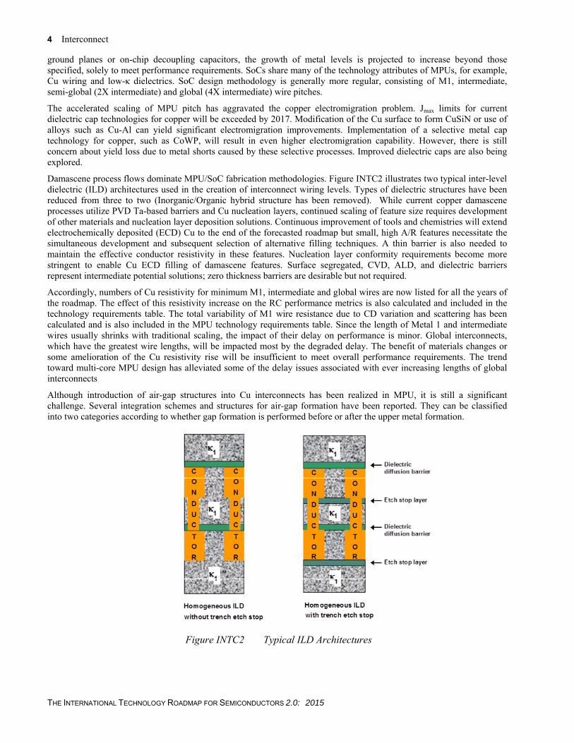


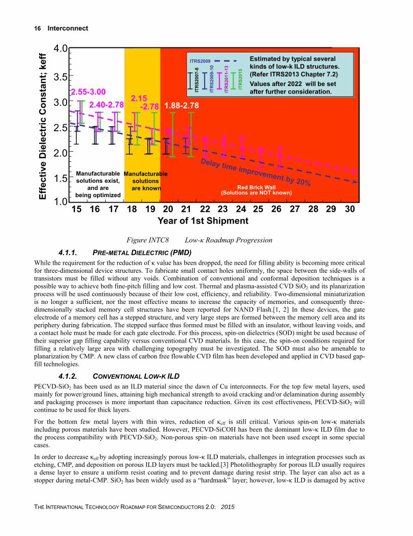


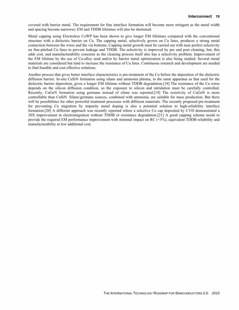
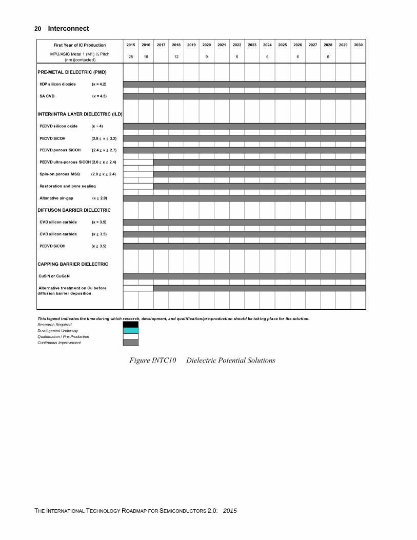


![ITRS 2001 Renewal - Work in Progress - Do Not Publish 1 [Per IRC Approved Proposals 3/27/01, Scenario 2.0/3.7] ITRS IRC/ITWG Meeting ORTC Proposal Review.](https://static.documents.pub/doc/80x56/55149715550346f06e8b5550/itrs-2001-renewal-work-in-progress-do-not-publish-1-per-irc-approved-proposals-32701-scenario-2037-itrs-ircitwg-meeting-ortc-proposal-review.jpg)


![ITRS Winter Conference 2007 Makuhara, Japan 1 International Technology Roadmap for Semiconductors 2007 ITRS ORTC [12/5 Makuhari Japan ITRS Public Conference]](https://static.documents.pub/doc/80x56/5514961d550346b0158b62f5/itrs-winter-conference-2007-makuhara-japan-1-international-technology-roadmap-for-semiconductors-2007-itrs-ortc-125-makuhari-japan-itrs-public-conference.jpg)

