108


iii
© Hamza Shahid
2017

iv
Dedicated to my parents and siblings

v
ACKNOWLEDGMENTS
All praise is due to ALLAH and peace be upon the Prophet صلى الله عليه وسلم and his family, his
companions (may ALLAH be pleased with them) and his followers.
Through utmost respect, I would like to share my inmost regards to my parents and my
family, without their prayers, moral support and love, I would not have been able to
accomplish my desired objectives in life. I will always be grateful to them for their
constant prayers, support and inspiration.
It has been my honor to be able to work with Dr. Hussain Abdullah Alzaher. I would like
to admire his supervision, suggestions and guidance right from the beginning till the end
of this research. His constant motivation helps me to produce quality work. I would like
to thank my committee members: Dr. Mohammad K. Alghamdi and Dr. Alaa El-Din
Hussein for their useful response, advice and the time they spent reviewing this thesis. I
am very obliged to King Fahd University of Petroleum & Minerals for providing me an
opportunity to pursue my graduate degree.

vi
TABLE OF CONTENTS
ACKNOWLEDGMENTS ............................................................................................................. V
TABLE OF CONTENTS ............................................................................................................. VI
LIST OF TABLES ........................................................................................................................ IX
LIST OF FIGURES ....................................................................................................................... X
LIST OF ABBREVIATIONS .................................................................................................... XII
ABSTRACT ............................................................................................................................... XIV
XVI ............................................................................................................................... ملخص الرسالة
CHAPTER 1 INTRODUCTION ................................................................................................. 1
1.1 Motivation ...................................................................................................................................... 4
1.2 Requirements from a sensor ........................................................................................................... 5
1.3 Thesis Objectives ............................................................................................................................ 6
1.4 Thesis Methodology ........................................................................................................................ 6
1.5 Thesis Contribution: ........................................................................................................................ 7
1.6 Thesis Breakdown ........................................................................................................................... 8
CHAPTER 2 LITERATURE REVIEW ..................................................................................... 9
2.1 Background: .................................................................................................................................... 9
2.2 Applications of Wireless Sensors:.................................................................................................. 10
2.3 Classification of Gas sensors based upon method of sensing ........................................................ 11
2.4 Evaluation of Gas Sensing Methods: ............................................................................................. 11
2.5 Approaches for Metal Oxides semiconductor based Gas Sensors:................................................. 14
2.6 Blocks of Wireless Gas Sensors: .................................................................................................... 15

vii
2.6.1 Sensor Front End: ..................................................................................................................... 16
2.6.2 Drawback of the approach: ...................................................................................................... 17
2.6.3 Low Noise Amplifier: ................................................................................................................ 18
2.6.4 Microcontroller: ....................................................................................................................... 20
2.6.5 Voltage/Current to frequency Converter: ................................................................................. 24
CHAPTER 3 GAS SENSOR: INTEGRATED CIRCUIT APPROACH ................................ 27
3.1 Sub hertz Oscillator ....................................................................................................................... 28
3.1.1 The feedback loop .................................................................................................................... 28
3.1.2 Relaxation Oscillator: ............................................................................................................... 30
3.1.3 Proposed Oscillator: ................................................................................................................. 32
3.2 Voltage Dividers ............................................................................................................................ 38
3.3 Buffer ............................................................................................................................................ 39
3.4 Wheatstone bridge ....................................................................................................................... 40
3.4.1 Micro-heater for gas sensor ...................................................................................................... 41
3.4.2 Noise analysis of Wheatstone bridge:....................................................................................... 45
3.5 Oscillator for excitation of Wheatstone bridge ............................................................................. 47
3.6 Analog Buffer ................................................................................................................................ 48
3.7 Difference Amplifier: ..................................................................................................................... 50
3.8 Switching Transistors .................................................................................................................... 52
3.9 Operation during the presence of gas ........................................................................................... 53
CHAPTER 4 RESULTS AND DISCUSSIONS ....................................................................... 55
4.1 Output of Sub Hertz Oscillator ...................................................................................................... 55
4.2 Output at Buffer Stage .................................................................................................................. 57
4.3 Characteristics of 1 KHz oscillator: ................................................................................................ 57

viii
4.4 Characteristics of Analog Buffer Stage .......................................................................................... 59
4.5 Characteristics at Wheatstone bridge: .......................................................................................... 60
4.6 Output Characteristics of Gas Sensor: ........................................................................................... 61
4.7 Summary of the Results ................................................................................................................ 74
4.8 Comparison with Other Sensors: ................................................................................................... 77
CHAPTER 5 POST LAYOUT SIMULATION........................................................................ 79
5.1 Layout for gas sensor circuit based on Schmitt Trigger based Timer. ............................................ 79
5.2 Post Layout Simulations for both configuration of gas sensors ..................................................... 80
CHAPTER 6 CONCLUSION AND FUTURE WORK ........................................................... 82
6.1 Conclusion .................................................................................................................................... 82
6.2 Future Work: ................................................................................................................................. 83
REFERENCES............................................................................................................................. 84
VITAE .......................................................................................................................................... 91

ix
LIST OF TABLES
Table 2.1 Advantages, disadvantages and applications of different Gas sensors ............. 14
Table 2.2 Power Consumption comparison for different sensor circuits.......................... 26
Table 3.1 Sizes of the transistors in Oscillator ................................................................. 38
Table 3.2 Sizes of 1 KHz oscillator circuit ....................................................................... 48
Table 3.3 Sizes for the Analog Buffer .............................................................................. 49
Table 3.4 Sizes for the difference amplifier ...................................................................... 52
Table 4.1 Summary for increase in Resistance of KΩ ...................................................... 74
Table 4.2 Summary of decrease of resistance in KΩ ........................................................ 75
Table 4.3 Summary of increase in resistance in MΩ ........................................................ 75
Table 4.4 Summary of decrease in resistance for MΩ ...................................................... 76
Table 4.5 State-of-the-art Gas Sensing Circuits: Comparative Study .............................. 78
Table 5.1 Comparison for both configurations ................................................................. 81

x
LIST OF FIGURES
Figure 1.1 Basic elements inside a general Sensor ............................................................. 2
Figure 2.1 General Applications of Wireless Sensors ...................................................... 10
Figure 2.2 Classification of Gas Sensing Methods ........................................................... 11
Figure 2.3 Approaches for Wireless Gas Sensors ............................................................. 15
Figure 2.4 Sensing front end circuits (a) Wheatstone (b) Voltage Divider ...................... 17
Figure 2.5 Typical application circuit for increased linearity. .......................................... 19
Figure 2.6 Tri-level comparator SAR ADC architecture .................................................. 22
Figure 2.7 Block diagram of frequency to digital converter ............................................. 23
Figure 2.8 Sensor heating profiles with time .................................................................... 24
Figure 2.9 Circuit diagram of a voltage controlled ring oscillator.[3] .............................. 25
Figure 2.10 Schematic circuit for source coupled multi-vibrator ..................................... 25
Figure 3.1 Flow diagram for the proposed sensor approach ............................................. 27
Figure 3.2 Positive feedback loop for bi-stable operation ................................................ 29
Figure 3.3 Bi-stable circuit with transfer characteristics .................................................. 30
Figure 3.4 Astable Multivibrator ...................................................................................... 31
Figure 3.5 Proposed CMOS based Oscillator ................................................................... 33
Figure 3.6 CMOS based Schmitt Trigger ......................................................................... 34
Figure 3.7 Voltage dividers for the circuit ........................................................................ 39
Figure 3.8 Inverter based buffer ........................................................................................ 40
Figure 3.9 Wheatstone bridge configuration of sensor front-end ..................................... 41
Figure 3.10 Typical micro-heater ..................................................................................... 42
Figure 3.11 Plate structure of micro-heater with hole in center ....................................... 43
Figure 3.12 Meander line structure ................................................................................... 43
Figure 3.13 Double Spiral Shaped .................................................................................... 44
Figure 3.14 Fan shaped Micro-heater ............................................................................... 44
Figure 3.15 Honey-comb Shaped Micro-heater ................................................................ 44
Figure 3.16 S-Shaped Micro-Heater ................................................................................. 45
Figure 3.17 Noise spectrum for resistive circuit ............................................................... 46
Figure 3.18 1 KHz oscillator for Bridge excitation .......................................................... 47
Figure 3.19 Analog buffer based on two stage op-amp .................................................... 49
Figure 3.20 Difference Amplifier ..................................................................................... 51
Figure 3.21 Transistor Switch ........................................................................................... 53
Figure 4.1 Output Characteristics of Sub-Hertz Oscillator with C=100p ......................... 56
Figure 4.2 Output Characteristics of Sub-Hertz Oscillator with C=50p ........................... 56
Figure 4.3 Output characteristics at buffer stage .............................................................. 57
Figure 4.4 Output of 1 KHz Oscillator ............................................................................. 58
Figure 4.5 Zooming in the waveform of 1 KHz oscillator ............................................... 58
Figure 4.6 Capacitor voltage for the 1 KHz oscillator ...................................................... 59
Figure 4.7 Output waveform of Analog buffer compared with capacitor voltage ............ 59

xi
Figure 4.8 Outputs of Wheatstone Bridge at equal transistors of 1KΩ ............................ 60
Figure 4.9 Outputs of Wheatstone Bridge at 1KΩ and 2KΩ resistors in one branch ....... 61
Figure 4.10 Output for the case of both 1 KΩ Resistors ................................................... 62
Figure 4.11 Output for the case of increase of 1% resistance ........................................... 63
Figure 4.12 Output for the case of increase of 5% resistance ........................................... 63
Figure 4.13 Output for the case of increase of 10% resistance ......................................... 64
Figure 4.14 Output for the case of increase of 20% resistance ......................................... 65
Figure 4.15 Output for the case of increase of 50% resistance ......................................... 65
Figure 4.16 Output for the case of increase of 100% resistance ....................................... 66
Figure 4.17 Output for the case of decrease of 5% resistance .......................................... 67
Figure 4.18 Output for the case of decrease of 10% resistance ........................................ 67
Figure 4.19 Output for the case 1MΩ - 1MΩ ................................................................... 68
Figure 4.20 Output for the case of increase of 1% resistance ........................................... 69
Figure 4.21 Output for the case of increase of 5% resistance ........................................... 70
Figure 4.22 Output for the case of increase of 10% resistance ......................................... 70
Figure 4.23 Output for the case of increase of 20% resistance ......................................... 71
Figure 4.24 Output for the case of increase of 50% resistance ......................................... 72
Figure 4.25 Output for the case of increase of 100% resistance ....................................... 72
Figure 4.26 Output for the case of decrease of 5% resistance .......................................... 73
Figure 4.27 Output for the case of decrease of 10% resistance ........................................ 74
Figure 4.28 Change of resistance for Wheatstone bridge ................................................. 76
Figure 4.29 Response of Sensor to the change in resistance of gas sensitive resistor ...... 77
Figure 5.1 Layout for first configuration of the gas sensor (layout floorplanning) .......... 80
Figure 5.2 Comparison of schematic and post-layout simulation for first configuration . 81

xii
LIST OF ABBREVIATIONS
WSN : Wireless Sensor Network
WPAN : Wireless personal area network
WLAN : Wireless local area network
GSM : Global System for Mobile communication
GPRS : General Packet Radio Service
CDMA : Code division multiple access
RFID : Radio-Frequency Identification
mW : milliwatt
ADC : Analog to digital converter
DAC : Digital to Analog Converter
CMOS : complementary metal-oxide-semiconductor
LNA : Low noise amplifier
GHz : Giga Hertz
GPS : Global positioning system
PWM : Pulse width modulation
AC : Alternating Current
DC : Direct Current

xiii
PMOS : P-type Metal Oxide Semiconductor
NMOS : N-type Metal Oxide Semiconductor

xiv
ABSTRACT
Full Name : [Hamza Shahid]
Thesis Title : Power Efficient Wireless Sensors for Gas Concentration Measurement
Major Field : [Electrical Engineering]
Date of Degree : [April 2017]
Wireless/mobile sensors have newly been considered in monitoring industrial applications
including risky gasses location. These types of sensors are of particular importance for the
Saudi industry in refineries and petrochemical plants. As a significant energy users, gas
sensors might essentially limit their lifetime. Hence, the sensing circuit is carefully
designed to optimize power consumption while achieving the desired performance and
accuracy. The metal oxide from which these sensors are made of (mostly SnO2-based), has
a range of temperature for sensing different gasses. Hence, the same sensor can be used by
different applications for measuring different gasses. The ideal temperature for metal oxide
(SnO2) to sense CH4 is 400 °C while it is 90 °C for CO.
The main objective of this thesis is to design a low power wireless sensors for gas
concentration measurement such that it can be utilized in the harsh environment for a long
period of time. Typical wireless sensor has main blocks of sensor front end, micro-heater,
microcontroller, power management, memory and communication block. After
microheater, the most power hungry component in sensor is microcontroller. The main
function of microcontroller is to provide the clock timing for the sensor operation. It is also
used for signal conditioning and memory. This work suggests adoption of a sub-hertz
oscillator, which has very low power consumption, for providing the timing for sensor
instead of the microcontroller. A microcontroller but at the receiver end, where utility
power sources are available, can be used to analyze the transmitted signal and add various
signal conditioning attributes. Several circuit techniques are utilized to achieve the purpose
of gas sensing more efficiently while keeping the sensitivity comparable and reducing
power consumption.
The sensor circuit uses two oscillators, a sub-hertz for providing the operating time of
sensor while the other for generation of AC signal to excite the Wheatstone bridge based
xv
sensor front end. The sub-hertz timer utilizes sub-threshold operation of transistors to
realize a CMOS inverter based Schmitt trigger. The current for charging and discharging
of capacitor is reduced in order to obtain ultra-low frequency oscillation. In addition, a
novel inverter based Schmitt trigger is proposed which is used to provide the AC signal to
sensor front end with improved sensitivity. The sensitivity of the wireless sensor is further
improved by using a high gain difference amplifier providing a gain of 63.5 V/V which
makes the output range of 1V for full scale variation. This allows to take the measurement
at lower temperatures when the resistance starts changing. The average power consumption
of the whole circuit is 38.77μW apart from the micro-heater power consumption. It is
possible to estimate the overall power consumption of the system by adding the power of
a commercial microheater and communication block to be around 2.07mW which is around
40 times less than the available solutions.
The thesis consists of seven chapters. The first chapter include an introduction, motivation,
the problem statement, an outline of objectives and the contributions. In chapter # 2,
literature review is discussed. A detail discussion on different specifications of wireless
gas sensors is presented in this section. In chapter #3, the approach towards achieving the
goal will be explained with all the circuits involved and their explanation. The results for
each stage as well as the final results are summarized in Chapter #4. Chapter # 5 contains
the new proposed Schmitt trigger for timer circuit. Chapter # 6 shows the post layout
simulation and Chapter # 7 consists of conclusion and future directions.

xvi
ملخص الرسالة
حمزة شاھد :الاسم الكامل
أجھزة استشعار لاسلكیة ذات كفاءة عالیة لاستھلاك الطاقة لقیاس تركیز الغاز :عنوان الرسالة
الھندسة الكھربائیة التخصص:
ھجري 1438-رجب-19 :تاریخ الدرجة العلمیة
تستخدم أجھزة الاستشعار اللاسلكیة / المحمولة حدیثا في رصد مواقع التطبیقات الصناعیة بما في ذلك الغازات الخطرة. ھذه
الأنواع من أجھزة الاستشعار ذات أھمیة خاصة للصناعة السعودیة في معامل التكریر والبتروكیماویات. لكن بسبب استھلاكھا
م التشغیلیة. وبالتالي، من المھم تصمیم دائرة الاستشعار بعنایة لتحسین استھلاك الطاقة مع لطاقة كبیرة، تحد أساسا من حیاتھ
)، وتتمتع SNO2تحقیق الأداء المطلوب والدقة. وتصنع ھذه الأجھزة الاستشعاریة من أكسید المعادن (معظمھا على أساس
لتالي، یمكن استخدام نفس أجھزة الاستشعار من قبل بأن لدیھا مجموعة من درجة الحرارة لاستشعار الغازات المختلفة. وبا
درجة مئویة 400المیثان ھي رتطبیقات مختلفة لقیاس الغازات المختلفة. فمثلاً درجة الحرارة المثالیة لأكسید المعادن لاستشعا
درجة مئویة لأول أكسید الكربون. 90بینما ھو
استشعار لاسلكیة منخفضة الطاقة لقیاس تركیز الغاز بحیث یمكن استخدامھا الھدف الرئیسي من ھذه الرسالة ھو تصمیم أجھزة
لاسلكي على كتل رئیسیة من أجھزة في بیئة قاسیة لفترة طویلة من الزمن. ویحتوي التكوین النموذجي لجھاز الاستشعار
المتحكم معظم تصالات. ویستھلكالاكتلة الاستشعار الأمامیة، سخان صغیر (میكروھیتر)، متحكم، إدارة الطاقة والذاكرة، و
طاقة أجھزة الاستشعار وذلك بعد المیكروھیتر. وتتمثل المھمة الرئیسیة للمتحكم في توفیر توقیت لعملیة الاستشعار على مدار
الذي الساعة. كما أنھ یستخدم لتحلیل الإشارات والذاكرة. ویقترح ھذا العمل استخدام مولد ذبذبات ذا تردد تحت واحد ھیرتز، و
یتمیز باستھلاك طاقة منخفضة جداً، لتوفیر التوقیت لجھاز الاستشعار بدلا من المتحكم. ویمكن استخدام متحكم ولكن في جھاز
الاستقبال، حیث تتوفر مصادر طاقة من المرافق، لتحلیل الإشارة المرسلة وإضافة سمات تكییف الإشارات المختلفة. ولقد تم
الدوائر لتحقیق الغرض من استشعار الغاز بشكل أكثر كفاءة مع الحفاظ على حساسیة مقبولة والتقلیل استخدام العدید من تقنیات
من استھلاك الطاقة.
دائرة الاستشعار المقترحة اثنین من مولدات التذبذب، احدھما مولد الذبذبات ذا تردد بمقدار ملیھیرتز لتوفیر وقت وتستخدم
تولید إشارة مترددة لإثارة جسر ویتستون في الجبھة الأمامیة للمستشعر. وتم تصمیم مولد التشغیل لجھاز الاستشعار والأخر ل
یتم حیث شمیت العاكس.-الترانزستورات تعمل تحت فاصل التشغیل موصلة على شكل زناد مالذبذبات ذا تردد ملیھیرتز باستخدا
شمیت -اقترح زنادبالإضافة الى ذلك تم فاض.شحن وتفریغ مكثف بصورة خاصة من أجل الحصول على التردد متناھي الانخ
عاكس جدید لاستخدامھ لتولید إشارة مترددة الواجھة الأمامیة للمستشعر والذي یتمتع بحساسیة محسنة. وتم تحسین حساسیة جھاز
1Vالى مرة مما یجعل نطاق الإخراج یصل 63.5الاستشعار لاسلكي أیضا باستخدام مكبر للفرق والذي یوفر مكاسب بمقدار
للتغیر الكامل لنطاق المقاومة المتغیرة. وھذا یسمح لأخذ القیاس في درجات حرارة أقل عندما تبدأ المقاومة تغییر. ویبلغ متوسط
میكرووات من غیر حساب استھلاك طاقة السخان الصغیر. ویمكن تقدیر إجمالي 38.77استھلاك الطاقة من الدائرة بأكملھا

xvii
مرات أقل من 40میكرووات وھو حوالي 2.072میكروھیتر التجاریة كتلة الاتصالات لیصل الى إضافةباستھلاك الطاقة
الحلول المتاحة.
وتتكون الأطروحة من سبعة فصول. ویتضمن الفصل الأول مقدمة، والدوافع، وبیان المشكلة، وموجزا للأھداف والمساھمات.
ت العلاقة مع مناقشة تفصیلیة بشأن المواصفات المختلفة لأجھزة استشعار الغاز ، یتم مناقشة المراجع العلمیة ذا2وفي الفصل
شرح النھج نحو تحقیق الاھداف مع شرح جمیع الدوائر المعنیة. ویتم تقدیم نتائج كل مرحلة وكذلك 3اللاسلكیة. كما یقدم الفصل
یقدم نتائج 6ید لدائرة الموقت. وفي الفصل رقم شمیت الجد-زناد 5. ویحتوي الفصل رقم 4النتائج النھائیة في الفصل رقم
والاخیر یتم عرض الاستنتاجات والاتجاھات المستقبلیة. 7المحاكاة بع التخطیط. وفي الفصل

1
1 CHAPTER 1
INTRODUCTION
A sensor is a device that can generate a useable electric signal from a measured physical
parameter of the environment. It provides the output as a function of changing the quantity
which is to be measured as an electrical signal, optical or electromagnetic signal. It can
measure the mechanical, calorific, chemical parameters just like, flow, speed, distance,
temperature, force, pressure, concentration, acceleration and composition of gases. For
example, a thermocouple senses the temperature and provides the output in the form of
electric signal while a mercury in glass based thermometer also senses temperature
variation and gives the output as expansion of mercury in the glass which can be seen and
measured.
In its simplest form, a sensor consists merely of a naked sensor element, for instance an
unhoused pressure sensor element made of silicon, mounted on a substrate, no more than
a few millimeters exterior dimension. The term “measuring principle” (also referred to as
the “active principle”) is understood to mean the principle of physical or chemical
conversion resulting in a usable electrical signal. A measuring parameter is converted into
an internal signal by means of the physical measuring principle of the sensor element. After
possible signal conditioning, a measured value is available at the output as a usable or
electrical signal – for example, luminous intensity as an analogue voltage. The basic
scheme is shown by Fig.1.1 [1]

2
Figure 1.1 Basic elements inside a general Sensor
Sensors are connected to the system via wire or wireless. Wireless sensors are more suitable
as they are cost effective, small, and easy to integrate than a typical wired sensor. Wireless
sensor are a medium applicable to observe a vast variety of environment parameters, for
example acceleration, temperature, pressure and also utilized for war zone observation,
environment observing, home automation applications and bio medical applications. Due
to the advancement of efficient sensor systems, WSN can be sent in applied in various
remote places and cruel climate conditions.
Different Sensing technology are extensively monitored and used for the sensing of the gas
detection. As there are various limitations of these gas detection technologies, there are
vast area of research for different methodologies for the researchers to work on and acquire
the solutions with improved calibration for gas sensors. These wireless sensors for gas
monitoring systems can be majorly classified according to change in electrical properties
of the material for sensing like [2]
Metal Oxide Semiconductors (MOS)
Carbon Nanotubes
Polymers

3
Moisture absorbing materials.
Different methods are utilized to acquire the results which are based on these types of
variations like [2]
Optical
Acoustic
Calorimetric
Gas-chromatography
In this thesis, the emphasis is based on the metal oxide semiconductor based wireless gas
sensors. A typical semiconductor based gas sensor is based on micro heater in a Wheatstone
bridge or in differential configuration. The micro heater heats the two special resistors in
the Wheatstone bridge or the differential configuration. The catalyst is applied over the
surface of one of the two sensors which burns in the presence of a gas over the surface of
the resistor and the resistance of that resistor with catalyst on the surface changes while the
other one remains the same. This provides the change of voltage at the output which is
detected by the micro-controller which compares this output voltage from the bridge with
the nominal value of no gas situation. If the output voltage is different, the micro controller
sends the interrupt signal to the receiver. The receiver then send the signal to the valves to
close to avoid any hazard.
4
1.1 Motivation
Wireless devices are one of the technologies on which large improvements are emerging
from past years. The range of these devices covers from basic IrDa which is based upon
infrared region for a short distances communication between a sender and a receiver to
WPAN for short distance but multiple receivers, to medium range communication in
WLAN, to far distance communication networks like GSM, GPRS and CDMA. [3]
The capacity to identify the events happened, is vital to the achievement of developing
wireless sensor technology. Wireless/mobile sensors offer an effective blend of the power
of sensing, manipulating and communicating with other devices. They are being used in
vast range of applications and, in the meantime, offer various trials because of their
characteristics, essentially the severe energy requirements which these sensors usually
face. The reduction in need of wiring and simplification of the circuit is a benefit of mobile
sensors. The experimentation stage in hardware platforms are been planned for the testing
of new incoming ideas given by the research community and how to implement those
design in the real world to get the desired outputs.
Mobile sensors bring the applications which were impossible without it, for example,
observing hazardous, dangerous, unwired or remote ranges and areas. The mobile sensors
give about huge installation adaptability to sensors and enhanced the efficiency of the
system. Besides mobile sensors lower the maintenance skills of the system and reduces the
expenses. Mobile sensors and sensor systems are widely used in farming and nourishment
generation for ecological observing, agriculture [4], food, monitoring of environment [5-
6], modern vehicles, building and office mechanization and RFID-based tracing
frameworks. [7]

5
1.2 Requirements from a sensor
A sensor should respond to the requirements for which it is designed. A sensor should
have following characteristics [2]
Uncertainty: Attainment of minimal measuring uncertainty.
Availability of Data: Constant availability of physical and chemical data from all
systems and processes
Impact: Measurements are to be performed with minimal impact on the processes
involved
Real Time: Measuring values are to be available in real time
Interference: Sensor should work with minimal interference and a minimum of
care
Cost: Sensor and sensor-system costs should be as low as possible
On Board Diagnostic: Sensors are to be equipped with integrated “on-board”
diagnostic
Ruggedness: It should be able to withstand the overload with the help of protection
provided.
Linearity: The sensor should have the linear input and output characteristics.
Repeatability: The sensor should give the same output when the similar input is
given to the sensor.
Quality: The sensor should give the high-quality output signal.
Reliability: The sensor should be reliable and stable. Sensors should function
without maintenance, calibration, or adjustment.
6
Dynamic Response: The sensor should have a vast dynamic response.
Hysteresis: The sensor should not show hysteresis
1.3 Thesis Objectives
The main objective of this work is to propose circuit techniques for designing a wireless
gas sensor with improved power consumption and hence increased the lifespan of the
sensor. This is accomplished by modifying the sensor front end to achieve the measurement
with desired sensitivity but with less power consumption. This allows taking the
measurement at lower temperatures when the burning of a specific gas starts. Also, the
proposed work applies the heating profile efficiently to get the desired results while
minimizing the power consumption. The results of the sensors can be applied to industries
containing hazardous gas (like petroleum and gas industry, chemical industries etc.) as well
as for environment monitoring in the industrial areas.
1.4 Thesis Methodology
The thesis work is divided into following tasks:
Task 1: Available solutions assessment and literature survey
Explore different industrial gas monitoring sensors and evaluate the performance
of these gas sensors.
Surveying application of different techniques to design a gas monitoring sensors.
Task 2: Design of sensor front end

7
Evaluating the two different approaches of Wheatstone bridge and differential
configuration for the sensor front end based on sensitivity and performance.
Task 3: Heating profile for the sensor
Analyzing heating profile to be applied to the micro heater to heat the sensor to the
required temperature efficiently.
Task 4: Assessing the approaches for output measurement
The different techniques will be assessed for measuring the change of resistance
from the sensor front end.
Task 5: Designing and simulation
The circuit design and simulations will be carried out in Cadence® and the output
results will be shown.
1.5 Thesis Contribution:
Gas sensors from the last decade is a very popular topic of research in academia and
industry due to the enhancement required for these kinds of sensors with the passage of
time. Wireless Gas sensors are beneficial over the wired sensors because of the harsh
environment in which the sensors have to work, cost of cables is reduced, and lower
maintenance is required as well as the fault can be easily detected. The major problem with
the wireless gas sensors are the huge power consumption, due to heating in CMOS and
other processes in different types of wireless gas sensors. Large power consumption
requires large supply power which is usually provided by batteries in the wireless sensors.

8
The batteries supply this power for the limited amount of time and there is need of
replacement of these batteries after a short time interval which creates a problem as these
sensors are usually located at unreachable places or in harsh environments, so the lifetime
of theses sensors is a major issue in the usage of theses sensors. Due to the high-power
consumption, energy harvesting techniques cannot provide the energy in milliwatt (mW)
range in indoor environment [8].
This thesis will contribute in the design of smart gas sensors for industrial monitoring for
which will be useful for the oil, gas, paint and other chemical industries in the kingdom of
Saudi Arabia as well as other countries.
1.6 Thesis Breakdown
The thesis consists of seven chapters. The first chapter include an introduction, motivation,
the problem statement, an outline of objectives and the contributions. In chapter # 2,
literature review is discussed. A detail discussion on different specifications of wireless
gas sensors is presented in this section. In chapter #3, the approach towards achieving the
goal will be explained with all the circuits involved and their explanation. The results for
each stage as well as the final results are summarized in Chapter #4. Chapter # 5 contains
the new proposed Schmitt trigger for timer circuit. Chapter # 6 shows the post layout
simulation and Chapter # 7 consists of conclusion and future directions

9
2 CHAPTER 2
LITERATURE REVIEW
This section discusses different approaches for wireless sensors applied in industry and
academia from past decade and summarize the different methods applicable to achieve
the function of gas monitoring by different techniques.
2.1 Background:
From the last decade, the sensing of the gas is one of the major application of industrial
safety and monitoring. The research is going on in academia as well as in industry for
making the sensors better and more energy efficient with every passing day. The common
areas Gas sensing technology has become more significant because of its widespread and
common applications in the following areas: (1) industrial production (e.g., methane
detection in mines) [9-10] ; (2) automotive industry (e.g., detection of polluting gases from
vehicles) [11] ; (3) medical applications (e.g., electronic noses simulating the human
olfactory system) [12] ; (4) indoor air quality supervision (e.g., detection of carbon
monoxide) [13] ; (5) environmental studies (e.g., greenhouse gas monitoring)
During the last fifty years, different studies have established various branches of gas
sensing technology. Among them, the three major areas that receive the most attention are
investigation of different kinds of sensors, research about sensing principles, and
fabrication techniques [14-15]. In these papers, a classification of sensing technologies is
given, followed by descriptions of the main technologies to provide a comprehensive
review. Two key performance indicators are highlighted, to introduce and compare

10
different sensing technologies. Current research status and recent developments in the gas
sensing field are reported, to discuss potential future interests and topics. Moreover,
suggestions on related topics' future development are also proposed
2.2 Applications of Wireless Sensors:
The general applications of Wireless sensors cover every field of science and technology,
from basic household items to complex systems of industries. Figure 2.1 shows the general
applications of wireless sensors. The basic areas are shown which can have the use of
wireless sensors in more than one applications in the respective area [9-19].
Figure 2.1 General Applications of Wireless Sensors
Gas sensing by the help of mobile sensor is becoming mere significant due to the utilization
of such sensors in the areas of (1) industrial production which includes the detection of
methane gas in the mines [9], (2) in the automotive industries which includes the detection
of gasses causing pollution coming out from the vehicles [11], (3) in the field of medical
regarding the detection of hazardous gases for human respiratory system [12], (4) the
11
monitoring of air quality inside a building which includes the detection of carbon monoxide
and carbon dioxide etc. (5) To study the environmental effects of different gases e.g. in the
monitoring of greenhouse gases [13]. Details of these areas will be mentioned in the of
literature review.
2.3 Classification of Gas sensors based upon method of sensing
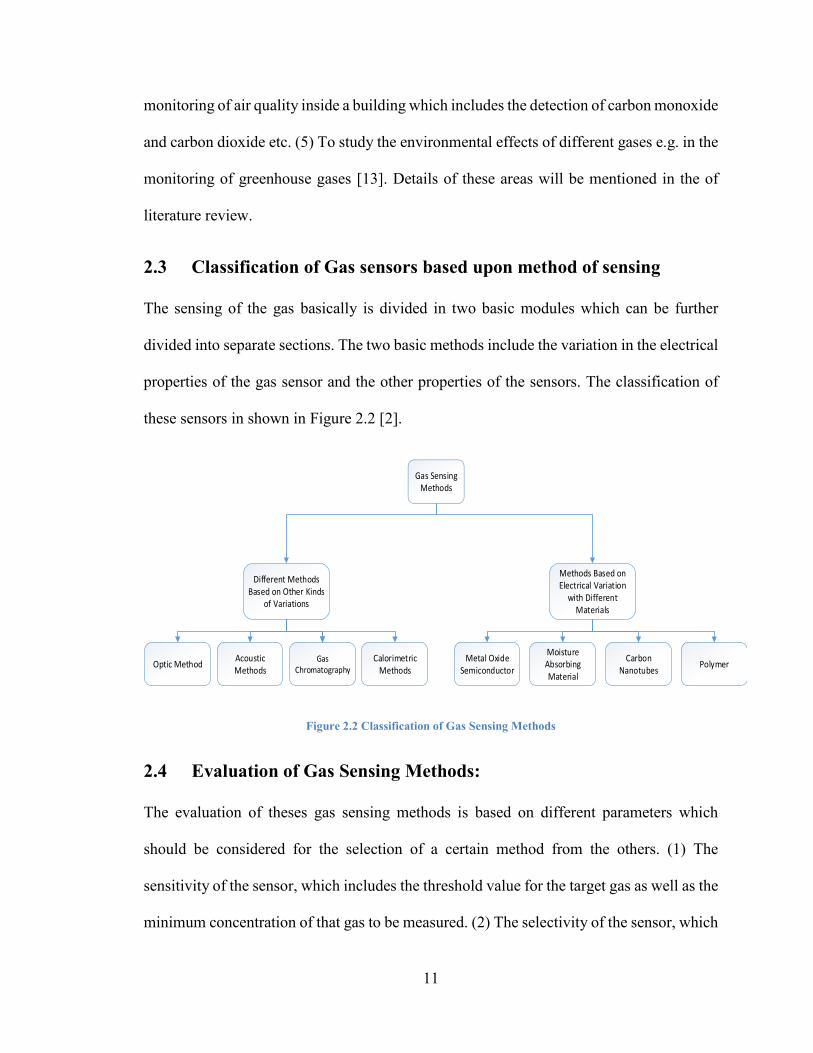
The sensing of the gas basically is divided in two basic modules which can be further
divided into separate sections. The two basic methods include the variation in the electrical
properties of the gas sensor and the other properties of the sensors. The classification of
these sensors in shown in Figure 2.2 [2].
Gas Sensing Methods
Methods Based on Electrical Variation
with Different Materials
Different Methods Based on Other Kinds
of Variations
Metal Oxide Semiconductor
PolymerCarbon
Nanotubes
Moisture Absorbing Material
Optic MethodAcoustic Methods
Gas Chromatography
Calorimetric Methods
Figure 2.2 Classification of Gas Sensing Methods
2.4 Evaluation of Gas Sensing Methods:
The evaluation of theses gas sensing methods is based on different parameters which
should be considered for the selection of a certain method from the others. (1) The
sensitivity of the sensor, which includes the threshold value for the target gas as well as the
minimum concentration of that gas to be measured. (2) The selectivity of the sensor, which

12
make sure to detect a certain gas when the combination of different gases are present. (3)
The response time of the sensor which includes the time between the concentration of the
gas to the certain value and when the sensor detects that and responds. (4) The energy or
power consumption of the specific sensor. (5) The reversibility of the sensor to its original
state after the measurement of a certain gas. (6) The absorbent ability of the sensor that it
can absorb the moisture and the reading is not affected by the moisture. (7) The cost of
fabrication for the sensor which can vary for the different methods and the usage of that
sensor in a particular environment. [14]
Although the sensors are designed to give the desired results for a long period of time and
their efficiency should remain the same but the performance of these sensors may degrade
with one of these reasons which can cause the major fail in the safety requirements of a
certain setup and a loss of human life and property may occur. (1) The design error in the
sensor which can be avoided by the careful inspection of the sensor in the test phase before
the commercial production. (2) The change or variation in the structure of the sensor when
the measurement is taken from it. (3) The lag or phase shift in the reading of the sensor due
to some additional doping on the sensing layer of the sensor. (4) The change in the chemical
properties of the sensor due to the chemical reaction of certain gas on the sensor. (5) The
effect of environmental factors which can alter the response of the sensor for a specific gas.
Table 2.1 shows the advantages, disadvantages and applications of these sensors. Usually
the gas sensors mostly used were based on film based, optical based or the semiconductor
and catalytic based. Film based sensors uses the combination of a colorimetric chemical
sensor along with the sensor for intensity of light [20]. The sensor receives the intensity of
light which is changed by the presence of hazardous gas in the form of change in color of
13
the film. These kinds of sensor although have very low power consumption but large
response time which makes them unsuitable for deployment by taking care of safety
requirements. Optical based sensors are employed with the help of laser-spectroscopic
trace gas sensors [20]. These sensors detect the little traces of gas concentration based on
calculation of ppm or ppb (parts per million or parts per billion). Although these sensors
are very accurate and response time is very less according to the safety requirements but
the power consumption of theses sensors is very high and draws a huge amount of current
(around 500mA) which makes them imperfect for wireless based sensors. The catalytic or
semiconductor based sensor are in between the two of them having the less power
consumption than the optical based sensors and are fast and selectable as compared to film
based sensors [2].

14
Table 2.1 Advantages, disadvantages and applications of different Gas sensors
So our prime interest will be on metal oxide semiconductor based wireless sensors for
compact low power sensors with acceptable sensitivity.
2.5 Approaches for Metal Oxides semiconductor based Gas Sensors:
The popular approaches for wireless gas sensors are described in Figure 2.3. Every
approach has its own advantages and disadvantages and one must critically analyze each

15
of them to be suitable for their target application. These approaches are analyzed and most
suitable configuration is used which is described in detail in the next chapter.
Figure 2.3 Approaches for Wireless Gas Sensors
The approach in (a) converts the front-end voltage /current to digital by the help of low
noise amplifier (OP amp based) and then ADC to convert the amplified signal into digital
[21]. The approach (b) converts the sensor front end voltage/current into frequency
dependent of incoming voltage /current and then a binary counter is utilized to convert that
frequency into digital output [22]. The approach (c) is utilized when the output required is
a voltage dependent frequency and that change in frequency determines the presence of a
specific gas [22].
2.6 Blocks of Wireless Gas Sensors:
Typically, the Wireless sensors has the followings blocks which will be described in a brief
detail in order to understand the purpose of each block.
16
2.6.1 Sensor Front End:
The sensor front end circuit is usually based on the Wheatstone bridge circuit, which
comprises of two sensing resistors and two normal resistors to complete the bridge circuit.
The power is generally consumed in the sensing resistors as compared to the other resistors
when the measurement is taken. CMOS based micro heaters are utilized to heat up the
resistances up to the required temperature with low power consumption and higher
efficiency [14]. One of the two sensing resistors is gas sensitive resistor due to the catalyst.
The catalyst is applied over the main measurement resistor and the reference sensing
resistors does not have catalyst on its surface. The oxidation of the gas starts at around 200
oC and the gas starts burning over the surface of the resistor. The change in resistance of
the sensing resistor with catalyst on the surface starts from this temperature but the change
is too small. It begins to increase with the increase of temperature. When the resistors are
heated to almost 400oC, the catalyst burns over the surface of main sensing resistor and its
resistance changes fully while the resistance of other sensing resistor without the catalyst
remains the same. The different output is obtained then the situation when gas is not
present. When gas is not present, the catalyst doesn’t burn and resistance of both sensing
resistances remains the same giving the zero output although if there is some change in
resistance due to high temperature, it is minimized due to the cancelling structure of
wheatstone bridge as it will come in both sensing resistors and will affect them equally
which will neglect the effect.
Due to the two-sensing resistor, the Wheatstone bridge configuration consumes more
power, the sensing front end sensor can also be based on voltage divider circuit which is
termed as differential circuit in [8] although it does not provide the differential output and

17
name is adopted as the output voltage changes with respect to the change in resistance and
then the difference is taken from the original value. Many articles in literature claims to
achieve low power consumption as there is only one sensing resistor and one reference
resistor as compared to the Wheatstone bridge which has two of both. The only difference
comes in the sensitivity of the sensor front end which is significantly reduced in the
differential based circuits as compared to wheatstone bridge. The circuit schematic of both
the approaches are shown in Fig 2.4 [8].
Figure 2.4 Sensing front end circuits (a) Wheatstone (b) Voltage Divider
2.6.2 Drawback of the approach:
The circuit suggested in (b) comes with only one sensing resistor and consumes less power,
but the issue of environmental factors is still there and the circuit is not much efficient. If
the resistance of the sensing resistor changes just due to very high temperature, it will give
the different output which can trigger the false alarm. The wheatstone bridge on the other
hand has four resistors with two sensing resistors and two reference resistors, the power
consumption is more. So we had to come up with the solution to resolve both the problems
while keeping the sensitivity as high as possible.

18
2.6.3 Low Noise Amplifier:
A low-noise amplifier (LNA) is an electronic amplifier that amplifies a very low-power
signal without significantly degrading its signal-to-noise ratio. An amplifier increases the
power of both the signal and the noise present at its input. LNAs are designed to minimize
additional noise. Designers minimize noise by considering trade-offs that include
impedance matching, choosing the amplifier technology (such as low-noise components)
and selecting low-noise biasing conditions.
LNAs are found in radio communications systems, medical instruments and electronic
equipment. A typical LNA may supply a power gain of 100 (20 decibels (dB)) while
decreasing the signal-to-noise ratio by less than a factor of two (a 3-dB noise figure (NF)).
Although LNAs are primarily concerned with weak signals that are just above the noise
floor, they must also consider the presence of larger signals that cause intermodulation
distortion.
The second stage in the sensor will be based on LNA (low noise amplifier). LNA should
be broadband to have a reliable matching of the input, more linearity, and the noise figure
should be low over a wide bandwidth of GHz, but having very little power consumption
and very small area to be easily fitted on a chip. The major challenge for the design of
ultra-wide band LNA is the linearity which should be high through all of the available
bandwidth. The optimization of the overdrive voltage is one of the methods to improve
linearity for the small input amplitudes and it will increase the response to the process
variation. It is usually effected by the low supply voltage and the mobility effects of high
fields [23]. The output from the first stage of sensor front end in the form of voltage or
current is then sent to a LNA. The measurement from the sensor front end has a very small

19
difference when the gas is present and when gas is not present. The low noise amplifier
voltage or current mode with a proper gain can be utilized at this stage to get the required
outputs.
The (MAX2659) low-noise amplifier has a large gain which is designed to be used portable
and handheld devices like GPS, GLONASS and Galileo. The amplifier is very ideal to be
used for a global positioning system to be added to a small navigational device as well as
cell phones to use this feature for personal mobility.
Although the MAX2659 has sufficient linearity for most of the system applications but still
we can improve the IP3 of the device. This is achieved by using a degeneration inductor
among the port number 2 which is the emitter of the amplifier and ground terminal, which
is described in Figure 2.5. This would increase significantly the IP3 meanwhile this will
reduce the gain of the amplifier along with the little degradation of the noise figure.
Figure 2.5 Typical application circuit for increased linearity.
The problem with these LNA is the huge power consumption in mW range, which makes
them difficult to use in low power solutions. The second thing is the use of inductors in the
circuit design which will make the integration difficult and CMOS realization of these

20
inductors will add power consumption of the circuit. Even a low voltage LNA having
supply voltage of 0.4V is having the power consumption of 1.03mW [24]. The
microcontroller can read the signal directly from sensor front end without the need of
amplification on the cost of such power. So, the LNA stage can be avoided in the design
according to the requirement of specific application of these wireless gas sensors.
2.6.4 Microcontroller:
The major block of these wireless gas sensor is the microcontroller unit which performs all
the required tasks for the wireless gas sensor. It works as a main control unit for all the
activities that are performing inside the sensor circuit. The micro controller is power
hungry element after the micro-heater in the gas sensor. The power in the range of mW is
required to carry out all the functions. These microcontrollers are very popular with the gas
sensors as they provide a wide range of possibilities which can be easily achieved with the
presence of microcontrollers with a little sacrifice of power consumption. So different
techniques such as pulse width modulation (PWM), on- off timing, heating profile, sleep
mode are used in order to save the power when using the microcontroller in the sensor
node.
The microcontroller consists of the blocks like programmable memory, comparators,
oscillators, ADC, DAC, timers/ counters, reset and power on circuits and they are also used
to control the other blocks like transmitters, receivers, supply control circuit etc. Typically,
these are targeted for the applications like
Industrial control
Climate control

21
Hand-held battery applications
Factory automation
ZigBee
Power tools
Building control
Motor control
HVAC
Networking
Optical
Medical Applications
Different microcontrollers are used in literature in order to achieve the desired result with
minimum power consumption. Atmel ATxmega32A4 is preferred in most of the sensors
due to small sleep current of 1 µA and 12bit ADC and DAC. During the operations, its
current is in mA as it controls all the function which includes the circuit management, the
heating profile of the sensor as well as communication with transmitter module. [25]
Following blocks of microcontroller are often used in the gas sensors for performing the
proper operation of the sensing.
2.6.3.1 Analog to Digital Converter (ADC)
One of the important block in a microcontroller is the availability of analog to digital
converter. The ADC will be required to convert the analog form of voltage or current to
digital form which can be easily transmitted to the receiver end. The resolution and power
consumption of ADC are important factors which must be considered according to the

22
required situation. The available types of ADC which includes SAR, Delta-Sigma and
Pipeline gives the range of resolution on the expense of power consumption. The SAR
ADC with maximum of 16 is usually utilized when it is used separately with minimum
power consumption of the three types. The microcontroller mostly used in gas sensors have
12-bit ADC in them like in ATxmega32A4 The typical power consumption of SAR ADC
for 9 bits of resolution is described as 1.2µW with max frequency of 1.1MHz in [26]. The
optimum condition is achieved with lower power of sensor front-end and a little more
power of ADC for better resolution at lower temperature will be followed in order to get
the acceptable results with overall low power consumption of the sensor. The low power
ADC proposed in [26] is shown in Figure 2.6.
Figure 2.6 Tri-level comparator SAR ADC architecture
The timing for the comparator is relaxed and the resolution of the ADC is reduced to one
bit by reducing the power consumption very low and very low supply voltage is required.
As for the gas monitoring sensor, very high frequency is not required and the process of
measurement only takes place once or twice in a minute so we can tradeoff the speed of
conversion and reduce the power consumption of the block.

23
2.6.3.1 Binary Counter:
Usually a 32-bit counter is available in the microcontroller that can even run during the
sleep mode in order to carry out the tasks such as heating of the sensor front end after a
specific amount of time. The counter/timers are really important for the microcontroller
to perform the required tasks. With the help of these counter, the sub hertz frequency is
achieved with the help of programming to turn on the heater after the specific amount of
time.
In the approach consisting of voltage/current to frequency converter. asynchronous
counters are usually utilized to convert the frequency generated in the voltage/current to
frequency converter block to digital values. The block diagram for the binary counter is
given in Fig. 2.7 [27].
Figure 2.7 Block diagram of frequency to digital converter
The counter is selected up to 9-bit resolution and the reference counter is also there to
compare the results for the reference frequency and the frequency we are getting from
previous stage. The comparison of the two is obtained the results are sent to next stage for
transmission to receiver end.
24
2.6.3.3 Sensor Heating Profile:
To save the power consumption of the wireless sensor, the sensors are not continuously
heated, instead they are heated after a regular interval as well as in different manners to
reduce the power consumption and get the required results. This is achieved by the
programming of microcontroller. The timer in the microcontroller runs even in sleep mode
to count the required time after which one level of voltage is applied to the sensor front end
and after required time, another value of voltage can be applied. This follows according to
the desired pattern fed through programming in the microcontroller. Some of the traditional
heating profiles are shown in Figure 2.8.
Figure 2.8 Sensor heating profiles with time
As the microcontroller is not used so the heating profile will be first one with two voltage
levels high and low produced by sub hertz timer.
2.6.5 Voltage/Current to frequency Converter:
The other approach from low noise amplifier and ADC is to use the voltage to frequency
conversion. The output voltage/current from the sensor front end is fed to the voltage
controlled ring oscillator which is composed of inverter which is followed by a TG
(transmission gate). The NAND gate is used to minimize the static power consumption in
idle state which prevents the needless oscillations. The frequency of oscillations is
determined by the change of resistance of the TG with the VH and VL from the sensor front

25
end stage. The output power is termed as 71 nW which is very suitable to be used in
wireless sensors for low power applications. [22]. The circuit schematic is shown in Figure
2.9
Figure 2.9 Circuit diagram of a voltage controlled ring oscillator.[3]
Another approach uses Buffered source-coupled Multi-vibrator circuit to generate the
frequency proportional to the change of output from the sensor front end. The low power
consumption of theses sensors is around 600nW with 0.9V supply. The circuit is capable
of providing waveforms with symmetry and also high frequency of oscillations. The circuit
schematic is shown in Fig 2.10 [27].
Figure 2.10 Schematic circuit for source coupled multi-vibrator

26
The cross coupled NMOS transistors will provide a gain stage that drives the load
resistance R. The switching in alternate cycles for the cross coupled transistors charges and
discharges the floated capacitor Co. The frequency of oscillations will be directly
depending upon the output voltage and input current and the value of capacitor [4].
�� =��
����� (2.1)
2.7 Benchmark table:
Table 2.2 shows some research work purely regarding the gas sensors and their power
consumption. [8]
Table 2.2 Power Consumption comparison for different sensor circuits
The trend of power consumption is given in mW for the references and still it is not a low
power circuit which can be operated totally on energy harvesting. The response time is
acceptable if it is less than a minute to avoid any loss of life and assets in the emergency
condition. By means of differential mentioned in the table, the author means the voltage
divider circuit.

27
3 CHAPTER 3
GAS SENSOR: INTEGRATED CIRCUIT APPROACH
This chapter begins with major idea of the proposed integrated approach towards the design
of wireless gas sensor. Instead of microcontroller, a sub hertz oscillator is proposed to
provide the on off timing for the sensor which is the prime objective of the microcontroller.
The secondary functions of microcontroller which contains the memory and signal
conditioning circuit is taken at receiver end and performed there to save the power. The
flow diagram for the proposed sensor approach is shown in figure below.
Figure 3.1 Flow diagram for the proposed sensor approach
The simulation is carried out in Cadence® with 0.15um CMOS technology and results will
be displayed. The main target of this approach is to reduce the overall power consumption
of the wireless sensor by keeping the sensitivity of the sensor as priority. Different energy
saving techniques as well as the steps to make the gas sensor smart are discussed in this

28
chapter with details. The multistage configuration is also demonstrated for larger DC
output voltage
3.1 Sub hertz Oscillator
The very first stage for the wireless gas sensor would be its timed on-off switching in order
to save power while maintaining the required time of operation. The micro-heater should
be heated in a pulsating manner instead of continuous manner which is the major cause of
power consumption in a wireless gas sensor. First challenge was to develop the timer/
oscillator which would provide that on-off timing to the sensor front end.
The oscillator required for this purpose was a square wave oscillator which have a logic
high and logic low to the switch which will provide current to the sensor front end. In this
way the sensor front end will be heated in a pulsated manner instead of continuous heating.
The next target was the introduction of pulse width modulation in the oscillator so that the
oscillator should provide logic high for a small unit of time and logic low for the large unit
of time in order to same maximum power. A bi-stable multi-vibrator is the circuit which
has two stable states and it can remain in one state until and unless the trigger makes it go
to the other stable state.
3.1.1 The feedback loop
The bi-stable function is achieved by a connection of an amplifier in the topology of
positive feedback with the closed loop gain more than unity. This feedback requires the
output to be fed back to the positive input in such a way that there is no phase shift between
the output and the input. The basic idea of positive feedback is considered with an example

29
of op-amp with output going back to positive input through the voltage divider circuit as
shown in Figure 3.2
Figure 3.2 Positive feedback loop for bi-stable operation
The circuit is working without any input and there is an assumption that a small noise is
there in every circuit and this noise will increase due to positive feedback to vi+. This will
continue to increase until the op-amp will saturate at the positive biasing voltages.
Similarly, if we start with the negative voltage, it will end in the negative biasing voltage
at the end. This is also termed as Schmitt trigger in this case.
Previously both the inputs of the circuit was at ground. Now if we connect a positive source
to the v+ of the op-amp. Initially we assume that the output of the op-amp is at L+ and hence
the feedback to v+ is ßL+. Now as the voltage at positive terminal of op-amp increases from
zero volts, the output remains the same until the input voltage reaches the level of v+. As
the input voltage exceeds this voltage, the negative voltage appears between the both input
terminals of the op-amp. The negative voltage will be multiplied by the open loop gain of
the amplifier and the output voltage will go negative. The feedback will provide that
negative voltage back to v+ which will start incrementing the output voltage until the
amplifier saturates at L-.

30
Further if the input voltage starts to decrease, the output will remain same until the input
voltage reduces further than the voltage at v+, which will make the difference between the
inputs of op-amp as positive and make the output of the amplifier positive. The positive
feedback will provide this voltage to v+ and hence increasing the output voltage until the
amplifier saturates at L+. The phenomena is shown in Figure 3.3.
Figure 3.3 Bi-stable circuit with transfer characteristics
3.1.2 Relaxation Oscillator:
The square waveform can be produced by making the bi-stable multi-vibrator to toggle its
two states in a periodic manner. The feature is produced by adding a RC circuit to a bi-
stable multi-vibrator in feedback loop. This has the inverting characteristics and the output
will go high and low with the charging and discharging of the capacitor. This way the

31
circuit has now no stable state and thus it is called astable-mutlivibrator [28]. The circuit
for the astable-mutlivibrator is shown in Figure 3.4.
Figure 3.4 Astable Multivibrator
The operation of the circuit will be such that assume the output of the circuit is at L+, the
capacitor will start to charge to this voltage through the resistance R. This voltage will
appear on v- of the op-amp which will start to increase towards ßL+ according to the time
constant CR. The voltage at v+ is already ßL+ and when the capacitor voltage reaches the
threshold equal to ßL+, the output will switch to L- and ßL- will appear on the v+ terminal.
The capacitor will now start discharging towards the ßL- and as soon as it reaches the lower
threshold, the output toggles again and shifts to L+. In this way, we will achieve the square
output from the relaxation oscillator.
The charging time for the capacitor is given by eqaution while Ƭ=CR is
�� = Ƭ ln�� ß�
����
�
�� ß (3.1)
Similarly, the discharging time for the capacitor is given by
�� = Ƭ ln�� ß�
����
�
�� ß (3.2)

32
If the charging and discharging time are equal which are obtained by L+ = L- then the time
period of the square wave is given by
� = 2Ƭ ln�� ß
�� ß (3.3)
3.1.3 Proposed Oscillator:
The usual oscillator of this type is based on the idea of a comparator with two bias voltages
which will decide the amplitude of the output whenever the signal goes above or below
these voltages. Ideal current sources supply the current to charge and discharge the
capacitor. If the charging and discharging currents are equal, then the frequency of the
timer will be given the formula which is not dependent upon the supply [28].
����
��(���� ���) (3.4)
These types of circuits have the problem of bias voltages and current sources, as the bias
voltages should be independent of process, the fluctuations in temperature and voltage
changes. The real challenge to reduce the power is to have a large time constant. This could
be either achieved through the large value of capacitor and resistor, but this will not be
suitable for integration. The other way is to reduce the current for charging and discharging
paths in order that the capacitor would require a large time to charge and discharge which
will increase the time constant. This low current can be achieved by either sub-threshold
current or the leakage current. The leakage current idea explained in [29] states that it
requires specific transistor to perform the leakage current. These special transistors have
different gate oxide thickness and only these kinds of transistors are allowing the leakage
current to flow. This solution cannot be much efficient as the leakage current is not a
33
constant current and with the passage of time, it may damage or degrade the performance
of the device. Secondly these special transistors may not be available for all kinds of
technology.
So, for the proper function of the circuit, we use normal transistor biased in sub-threshold
region to minimize the current for charging and discharging paths of capacitor. The other
techniques are utilized as well to minimize the current which will be discussed after the
Figure showing the circuit for the proposed oscillator.
Figure 3.5 Proposed CMOS based Oscillator
The function of comparator for this purpose is performed by CMOS based Schmitt trigger
instead of op-amp based Schmitt trigger to save power consumption which is the major
issue of the circuit. The sections are described in detail separately along with the functions
of each block.

34
Figure 3.6 CMOS based Schmitt Trigger
The standard cascade architecture used in the CMOS Schmitt Trigger circuit design [12] is
shown in the Figure 1 limits lowering of the operating voltage. The operation of the Schmitt
Trigger circuit is as follows. Initially, IN = 0 V, the two-stacked p-MOSFET (M6 and M7)
will be on. Hence OUT = VDD. When IN rises to VTN, M9 is on. But M8 is still off since
M11 is on and source voltage of M8 is VDD. Now both M8 and M9 are on, OUT
approaches to 0V rapidly and M11 becomes off. When IN approaches VDD, the two-
stacked n-MOSFET (M8 and M9) will be on. Hence OUT =0. When IN falls to |VTP|, M6
is on. But M7 is still off since M10 is on and source voltage of M7 is 0 V. Thus, source
voltage of M7 is rising with decreasing IN. When source voltage of M7 rises to |VTP|, M7
is on. Now both M6 and M7 are on, OUT approaches to VDD rapidly and M10 becomes
off.
VOH is the maximum output voltage and VOL is the minimum output voltage. Vhl is the
input voltage at which output switches from VOH to VOL. Vlh is the input voltage at which
output switches from VOL to VOH. Vhw is called the hysteresis width.
��� =��� − ����
� + 1

35
��� =�|��� |
� + 1
��� = ��� − ��� =��� − �(��� − |��� |)
� + 1
Where R is the ratio of n- and p-MOSFETs’ transconductance parameters respectively.
� = ���
��
The threshold voltage can be calculated for MOSFET by the following equation.
��� = ��� + ɣ� |− 2ø� + ��� |− � |2ø� |
Where
ɣ = ����
����� 2������
VSB is the source-to-body substrate bias, 2ø� is the surface potential, and ��� is threshold
voltage for zero substrate bias.
The CMOS based Schmitt Trigger is biased in threshold voltage. Input to the Schmitt
trigger is the capacitor voltage which is either charging or discharging shape. The Schmitt
trigger is based on inverter circuit and when charging input is there the output is logic zero
and when discharging output is there the output is logic one.
The next stage for the Schmitt trigger is the inverter to maintain the positive feedback in
order maintain the oscillations. The output of the inverter is fed back to the transistors as
switches which will allow vdd and gnd to connect to the capacitor and the charging and

36
discharging. The charging of the capacitor is carried out through PMOS which will be on
when it gets the output low from the feedback circuit. When the PMOS turn on in sub
threshold region, in order to get the long off time for the output, the charging current is
further divided into two unequal paths by two parallel PMOS transistors M12 and M13
which will pass the smaller ration of current to charge the capacitor through M12. This will
increase the off time up to 40 seconds with the capacitor value of 100pF. Similarly, the
discharging path is turned on by NMOS and size of NMOS is kept bigger than PMOS in
order to have smaller time for discharge so that the output will be on for a smaller time
according to the requirement. M14 and M15 serves as voltage divider to provide the
required voltage to M16 to provide the suitable discharging time of capacitor. To alter the
time size of M14 and M15 is changed until the required results are obtained.
The charging and discharging time of the oscillator can be changed by varying the size of
charging and discharging path switching transistors. The maximum half period we are
getting with 100pF capacitor is around 44 seconds. For the applications which require more
time period, a capacitor can be added in parallel with 100pF capacitor which would
increase the time period of the oscillator.
In sub threshold operation, the current through MOSFET is the exponential function of
Vgs and Vds and is given by
��� ������������ = ������ � ���
�ø� �1 − �
� ����ø� �
�� = ���
�
�(� − 1)ø�
�

37
ø� =��
� ≈ 26��
If ��� > 3ø� ≈ 78�� , �1 − �� � ��
ø� � ≈ 1.
The charging current through M1 is calculated first. As Vds is greater than 78mV so the
effect of Vds will be eliminated in the calculation of current and will only depend upon the
Vgs of M1. This will be the total current through M1 which is split in two branches with
PMOS with unequal sizes to divide the current in such a way that less current goes towards
the charging of capacitor. (W/L)M13 > (W/L)M12
�� � = �� �� + �� ��
The charging current can be found directly by taking the ratio of sizes of transistors or by
substituting the values in above equations to find the both currents separately. The
Charging current will be taken as average because it is maximum when the capacitor is
uncharged and it goes less when the capacitor is charged to the maximum value.
Similarly, for discharging of capacitor, NMOS block consisting of M14, M15 and M16.
The gate voltage of discharging transistor M16 is divided by two transistors M14 and M15
in order to reduce the discharging current and increase the discharging time for the
capacitor. Vgs can be calculated by taking the ratios of sizes of M14 and M15. The current
can be found through the current equation in subthreshold. Here again the Vds is larger so
effect of Vds will be neglected.
The charging and discharging times can be calculated by the following equations. During
the charging time the output is low while during discharging period the output is high.
38
��������� =�����
���������
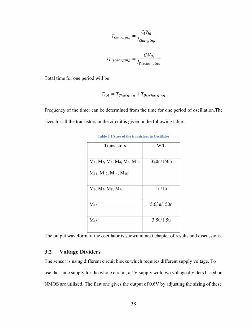
������������ =�����
������������
Total time for one period will be
���� = ��������� + ������������
Frequency of the timer can be determined from the time for one period of oscillation.The
sizes for all the transistors in the circuit is given in the following table.
Table 3.1 Sizes of the transistors in Oscillator
Transistors W/L
M1, M2, M3, M4, M5, M10,
M11, M12, M14, M16
320n/150n
M6, M7, M8, M9, 1u/1u
M13 5.63u/150n
M15 3.5u/1.5u
The output waveform of the oscillator is shown in next chapter of results and discussions.
3.2 Voltage Dividers
The sensor is using different circuit blocks which requires different supply voltage. To
use the same supply for the whole circuit, a 1V supply with two voltage dividers based on
NMOS are utilized. The first one gives the output of 0.6V by adjusting the sizing of these

39
transistors. The second voltage divider takes the 0.6V and provides 0.4V by sizing the
transistors properly. The 0.4V is utilized by sub-hertz oscillator and 0.6V is utilized by
the buffer. Rest of the circuit works with 1V supply.
Figure 3.7 Voltage dividers for the circuit
3.3 Buffer
In order to drive all the circuits with this timing oscillator, the digital buffer is required.
This buffer performs two functions, one is to provide the function of buffer and second is
the voltage level shifting from 0.2V to 0.6V for the proper operation of transistor switch in
strong inversion. The inverter used in the oscillator is cascaded with another one in order
to give the output as buffer. The difference between the normal inverter based buffer and
this one is that it is changing the input signal of 0.4V amplitude to 0.6V output. The first
inverter is having the supply voltage of 0.4V while the 2nd stage is having the supply
voltage of 0.6V. These voltages are generated from the main supply of 1V. All the
transistors from M17 to M24 are in sub-threshold region with minimum W/L of 320n/150n.
The buffer is shown in Figure 3.8

40
Figure 3.8 Inverter based buffer
3.4 Wheatstone bridge
The sensor front end is connected in the topology of Wheatstone bridge in order to get
maximum sensitivity although by differential mode, 2 resistors are less and they will save
the power but it has degraded sensitivity as compared to wheatstone bridge. With better
sensitivity, we can detect the presence of gas earlier than the differential circuit and this
will save the power by not heating the sensor to full 400°C. As the major cause of power
consumption is the micro-heater heating the sensor.
The R2 is the gas sensitive resistor which has catalyst applied over the surface and R3 is the
resistor with no catalyst. Different values of resistances are used in literature for the sensor
front end. This mainly depends upon the material used to fabricate the micro-heater and
that will have its specific resistance. So, in literature the values of Ω, KΩ and MΩ are used
[8], [21], [27] and we have tested the bridge for all these ranges of resistances. In the
presence of gas, the gas sensitive resistor can change the resistance up to twice depending
upon the material being used to create these resistances. Even in low resistance case it
might increase more than twice [8], so we have analyzed the change of resistance right

41
from the start of 1% to 100% and even more in case of low resistances. The results are
discussed in next chapter of results and discussion. The Wheatstone bridge configuration
is shown in Figure 3.9.
Figure 3.9 Wheatstone bridge configuration of sensor front-end
3.4.1 Micro-heater for gas sensor
Micro-heater is an essential part of gas sensor as it must heat the resistor to the required
temperature to sense the presence of gas in the surrounding atmosphere. These micro-
heaters are fabricated with different materials and different designs to get maximum
efficiency of heating with minimum power consumption. The basic configuration of a
typical micro-heater is shown in the Figure 3.10.
The main block consists of two resistors baked inside a single housing. One of them is the
heater resistor Rh which heat up to the required temperature when the current pass through
it and the heat of this resistor is passed to the resistor which is connected for the
measurement in the circuit. Catalyst is applied over the surface which burns in the presence
of gas which changes the resistance of the gas sensing resistor Rs [30], [37-38]

42
Figure 3.10 Typical micro-heater
The design of micro heater is vastly present in the literature which have a huge diversity
in shape, size, patterns and materials in order to have maximum resultant heating with
minimum power consumption. Still today the power consumption of these micro-heaters
is in mW [31-33]
3.4.1.1 Geometries of micro-heater:
The micro-heaters are fabricated in different patterns to get the desired performances as
there are different kinds of heat loss through conduction, convection and radiation
phenomena. Some of the shapes are described briefly here as
Plane plate structure with hole in center: By this design, the process of natural
convection takes place. Due to the hole in the center of the structure, the problem
of uneven and random appearance of hot spots near the center and the power
consumption of these structure is high. The structure is shown in Figure 3.11.

43
Figure 3.11 Plate structure of micro-heater with hole in center
Meander line structure: These structures have 90° turns for the meandering
structure which takes a small area instead of a straight-line structure. The problem
with this structure is the creation of hot spots with high temperatures around the
bends which will cause uneven heating. The structure is shown in Figure 3.12.
Figure 3.12 Meander line structure
Double spiral shaped: Due to the problems of meander design of micro-heater, a
double spiral shaped micro-heater were created with variable gap between the lines
and variable widths of the line inside the pattern. The shape is shown in the Figure
3.13.

44
Figure 3.13 Double Spiral Shaped
Fan shaped Micro-heater: The modification of double spiral shaped micro-heater
creates the fan shaped micro-heater. This design is one of the best design to achieve
uniform heating along with the very low power consumption. The structure is given
in Figure 3.14.
Figure 3.14 Fan shaped Micro-heater
Honey-comb Shaped Micro-heater: This design of micro-heater allows the
redistribution of thermal energy and provides the uniform heating profile. The
structure is given in Figure 3.15.
Figure 3.15 Honey-comb Shaped Micro-heater

45
S-Shaped Micro-Heater: This design is also very suitable for the low power
consumption and uniform heating but is only used for small sized sensing
structures. The structure is given in Figure 3.16.
Figure 3.16 S-Shaped Micro-Heater
3.4.2 Noise analysis of Wheatstone bridge:
In several applications, Wheatstone bridge with resistive bridge elements constitute the
front end and are excited using the DC supply and the reading is taken at very low
frequency. Although all resistive elements exhibit small amount of Nyquist noise but in
this particular case, 1/f noise will dominate and will be the biggest source of noise as you
will go low in frequency.
The solution of this problem to avoid 1/f noise is to excite the bridge using AC. The
frequency of AC should not be very high and it will be cleared in next section that what
minimum frequency of AC will solve the problem of 1/f noise. Following are the types of
noise that effects the resistive Wheatstone bridge.
3.4.2.1 Nyquist Noise:
Nyquist noise also known as thermal noise exists in both AC and DC excitation for
resistive bridge measurement circuit. This is due to the motion of particles (electrons)
inside the resistance which does not depends upon any supply voltage. The response of

46
such noise has white spectrum and it exists in all the frequency bands. The effect of this
noise cannot be removed completely but it can be reduced by decreasing the bandwidth.
3.4.2.2 Shot Noise:
Whenever the current flows through the resistor, the noise may appear in the form of an
opposing voltage which is termed as shot noise. It occurs due to random fluctuations in the
flow of current. In order to avoid this noise, we must avoid the large amount of current
through the resistors which will result in the presence of shot noise.
3.4.2.3 Flicker Noise:
The flicker noise of 1/f noise typically exists in the electronic systems at low frequencies,
normally when we go below 100 Hz. As there is inverse relation between the noise and
frequency so it rises with the decrease of frequency towards DC. The sources of this noise
are random fluctuations in any parameter of the circuit.
So, combining all the facts the noise spectrum for the resistive network is shown by the
Figure 3.17 [34]
Figure 3.17 Noise spectrum for resistive circuit
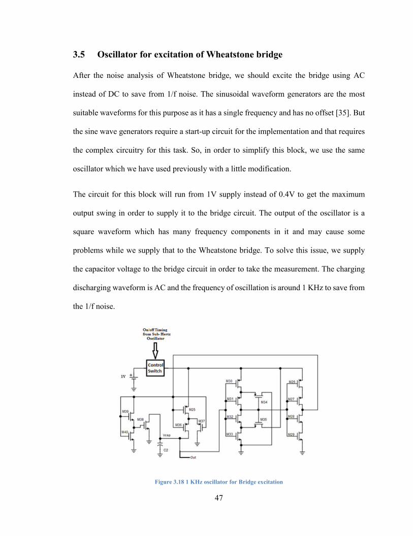
47
3.5 Oscillator for excitation of Wheatstone bridge
After the noise analysis of Wheatstone bridge, we should excite the bridge using AC
instead of DC to save from 1/f noise. The sinusoidal waveform generators are the most
suitable waveforms for this purpose as it has a single frequency and has no offset [35]. But
the sine wave generators require a start-up circuit for the implementation and that requires
the complex circuitry for this task. So, in order to simplify this block, we use the same
oscillator which we have used previously with a little modification.
The circuit for this block will run from 1V supply instead of 0.4V to get the maximum
output swing in order to supply it to the bridge circuit. The output of the oscillator is a
square waveform which has many frequency components in it and may cause some
problems while we supply that to the Wheatstone bridge. To solve this issue, we supply
the capacitor voltage to the bridge circuit in order to take the measurement. The charging
discharging waveform is AC and the frequency of oscillation is around 1 KHz to save from
the 1/f noise.
Figure 3.18 1 KHz oscillator for Bridge excitation

48
The capacitor for this oscillator is 5pF and the output is taken from the capacitor node
which will supplied to the next stage. The W/L ratio of these transistors are given in the
table 3.2
Table 3.2 Sizes of 1 KHz oscillator circuit
Transistors W/L
M25, M26, M27, M28, M29,
M34, M35, M36, M38, M39
320n/150n
M30, M31, M32, M33 1u/1u
M37 10u/1u
M40 320n/200n
The output waveform is show in next chapter with title of results and discussions. The same
phenomena of PWM is used to control the charging and discharging time for the capacitor
but here the charging and discharging time are almost equal.
3.6 Analog Buffer
In order to supply the AC waveform, form the oscillator to bridge circuit, analog buffer is
required in order to avoid the oscillator from loading effect. The analog buffer is based on
simple two stage op-amp, with PMOS as differential input stage. This stage gives the open
loop gain of 40dB with power consumption in nW. When connected in closed loop for
buffer, it gives the loose and not performing as a proper buffer. So, in order to enhance the
gain and better performance, a CS stage is added and the buffer configuration is achieved.

49
Input waveform from the oscillator stage is buffered and applied to the wheatstone bridge
for the measurement. The op-amp buffer is shown in Figure 3.19.
Figure 3.19 Analog buffer based on two stage op-amp
As the input signal has a DC offset due to the type of input signal which is the charging
and discharging waveform between the upper and lower thresholds. The offset in the input
is always multiplied by the gain and that offset appears in the output. As the op-amp is used
as a buffer so its closed loop gain is around one and the DC offset almost remains the same
after passing through the buffer stage. The W/L for the buffer circuit are given in the table
3.3.
Table 3.3 Sizes for the Analog Buffer
Transistors W/L
M41, M47, M44, M45 1u/1u
M42, M43 1u/700n
M46 50u/1u

50
3.7 Difference Amplifier:
When the Wheatstone bridge is excited with the AC signal from the oscillator through
buffer, it enters both the branches of Wheatstone bridge with equal impedance and the
differential output of the bridge will be zero in this case. When the gas is present, the
resistance of the gas sensing resistor will change which will cause the output of that branch
of Wheatstone bridge to change and the differential output of the Wheatstone bridge will
not be zero. This would be a very small value and will be difficult to monitor for every
small change like 1% in the resistance. In order to get the difference from the outputs of
Wheatstone bridge amplified, the difference amplifier is used based upon op-amp.
The main idea is to have much more gap between every 1% change of resistance that it can
be easily monitored. For that purpose, we require a high closed gain from the amplifier.
This may cause a power consumption but still we will be able to detect the gas at very early
stage as compared to the detection after a specific amount of time. The power consumption
of such circuits is usually in hundreds of microwatts which will be still better than using
the micro-controller with mW of power consumption.
The difference amplifier is used to take the difference between the input signals and rejects
any common signal to both of them. An ideal difference amplifier should have the zero-
common mode output and a fixed gain output in differential mode [28]. The output of the
difference amplifier is given as
�� = ����� + ������� (3.5)
Where Ad is the differential gain, vid is the differential input, Acm is common mode gain
and vicm is common mode input for the amplifier. The amplifier we are using is the two

51
stage op-amp with input differential stage implemented with PMOS transistors and the
second stage with a common source amplifier. The ratio of resistors for the feedback path
to input path is 70:1 such that we are getting the gain of 63.5 for the output signal. The
input signal is has the full scale change from 0.0798mV to 7.412mV when the resistance
change is from 1% to 100% for which the output will have the range from 5.067mV to
471.36mV for the same amount of change. The circuit for the difference amplifier is shown
in Figure below. The input is having the offset of around 30mV which is reduced by
negative feedback but the remaining one is multiplied by the gain and appears in the output.
When the difference of resistance occur, it also changes the amplitude as well as the offset
in the particular branch of Wheatstone bridge. So the inputs going to difference amplifier
have different amplitudes as well as different offset. The supply voltages are 1V and -1V.
Figure 3.20 Difference Amplifier

52
The sizes for these transistors are shown in table below. These values are selected in order
to make all the transistors in pinch-off mode in order to get maximum gain out of the
amplifier so that the output may have a large variation with the change in input.
Table 3.4 Sizes for the difference amplifier
Transistors W/L
M48, M53, M54 10u/700n
M49, M50 10u/1u
M51 , M52 12u/1u
The output waveforms will be discussed in detail in the next chapter of results and
discussions as well as the comparison tables and graphs will be displayed.
3.8 Switching Transistors
In order to make all the circuit working only in the time when the sub-hertz oscillator have
logic level high, the switches based on transistors are used. Although a single transistor can
be used as a switch like NMOS where the drain is connected to supply and gate to the
control signal and source to the circuit where the supply has to be delivered. But taking the
output from source will not give the efficient results. So in order to maintain the efficiency
a combination of NMOS and PMOS are used where NMOS is used as common source and
PMOS as common drain. This combination allows the perfect switch and maximum power
transfer. The switch is shown in Figure below

53
Figure 3.21 Transistor Switch
3.9 Operation during the presence of gas
During the normal operation of gas sensor with no gas, the output of the difference
amplifier will be almost zero. The nominal heating time for the microheater varies between
0.4sec – 2.5sec [8], [36]. The nominal time it takes to cool down back to the IC temperature
takes 0.2 sec to 2sec depending on the construction of microheaters [36-37]. Normally
these gas sensors are operated once between 20sec- 60sec depending upon the location and
type of gas being monitored. The readings are taken keeping the above timings in
considerations so for experiment, the on time for sensor for heating is chosen close to
maximum time that is 2sec and 44sec for sleep time provided by sub-hertz timer. During
this time, not only microheater, but the whole circuit is turned off as the supply to all the
circuit goes through the switch operated by the same sub-hertz timer. The power
consumption will only for the time of operation of the circuit and average power
consumption is calculated for the whole period.
The output of difference amplifier with the amplitude and offset will depict the presence
of gas and the reading will be sent to receiver end where the reading would be analyzed

54
and return the status to continue the operation if the gas is not present. Later, when the gas
will be present, the output will be shown so in order for the safety of the location, the sensor
will not take the reading after 40 seconds but instead it will continue to take the reading
until and unless the presence of gas is eliminated [40]. In order to propose this feature for
future, a comparator with output connected to switches consisting of NMOS and PMOS
with gates connected together for input will be added. The drain of NMOS is connected to
the main supply while the PMOS is connected to the output from sub hertz oscillator. When
the gas will not be present output will be zero and PMOS will be on to supply the normal
sub hertz on time for the sensor but when the gas will be present the output will turn on
NMOS and turn off PMOS and sensor will be connected directly to the supply for
continuous mode of operation until the sensor is reset or if the gas eliminates from the
premises.

55
4 CHAPTER 4
RESULTS AND DISCUSSIONS
This chapter will discuss the results and discussions for the blocks described in previous
chapter. The output waveform of each block will be separately and also the required
conditions will be discussed. The comparison tables along with the different graphs will
also be displayed.
4.1 Output of Sub Hertz Oscillator
The sub hertz oscillator is working with the voltage of 0.4V and all the transistor are in
sub-threshold region. The capacitor used is of 100pF in order to get the frequency of 0.0217
Hz. In order to get more low frequency, the capacitor in parallel have to be added. The
charging time for the capacitor is 44 seconds which will keep the output low for this time
and discharging time for the capacitor is 2 seconds for which the output will be high.
The Schmitt trigger sets the upper threshold voltage at 68.9 mv while the lower threshold
is kept at 20.32 mv keeping the capacitor voltage to swing between these thresholds and
maintaining the output amplitude of 48.58mV for the capacitor voltage. The output of the
oscillator switches between 0V and 216.5 mV. The output waveform of oscillator and the
capacitor voltage is shown below

56
Figure 4.1 Output Characteristics of Sub-Hertz Oscillator with C=100p
By changing the value of capacitor to lower value, we can get a fast response for the
oscillator and by changing W/L of charging and discharging paths we can adjust the PWM
as well. Now making the value of capacitor as 50pF and frequency of oscillation changes
to 0.05Hz. This phenomenon can be adapted for the sensors which are located in the
sensitive areas and they require getting the reading faster as compared to the other places.
The output characteristics with half the value of capacitor is shown below.
Figure 4.2 Output Characteristics of Sub-Hertz Oscillator with C=50p

57
4.2 Output at Buffer Stage
The next stage of oscillator was the digital buffer in order to provide the output of the
oscillator to later circuit with the amount of voltage which can be served to turn on and off
the transistor in linear or pinch-off region. The inverter based buffer uses the 0.4V for the
first inverter and 0.6V by the second buffer. The input to the buffer is the square waveform
with values of 0V and 216.5mV while the output from the buffer is between 0V and
600mV. The output at the buffer stage is shown in Figure 4.3.
Figure 4.3 Output characteristics at buffer stage
This output is supplied to the switches to turn on the other parts of circuit during this time
and for the other time, all the other circuits should be off in order to save the power.
4.3 Characteristics of 1 KHz oscillator:
The output of buffer is applied to switch which connects the 1 KHz oscillator with 1V
supply voltage and it starts giving the output. The value of capacitor is 5pF for this
oscillator. We make the charging and discharging paths equal in order to get a proper output
waveform.

58
Figure 4.4 Output of 1 KHz Oscillator
Zooming that waveform, we get the output of the oscillator as follows
Figure 4.5 Zooming in the waveform of 1 KHz oscillator
The frequency comes out to be around 1 KHz for the oscillator but we have to use the
capacitor voltage of this oscillator to be used as output for the next stage to excite the
Wheatstone bridge. So, the capacitor voltage waveform with same frequency is given by
the following Figure 4.6. The waveform has the offset of about 100mV while the swing is
between 130mV to 68mV making the amplitude of the capacitor voltage to be around
62mV.

59
Figure 4.6 Capacitor voltage for the 1 KHz oscillator
4.4 Characteristics of Analog Buffer Stage
The next stage after the 1 KHz oscillator will be the analog buffer in order to provide the
capacitor voltage to the load of Wheatstone bridge and avoiding any loading effect on the
oscillator. The op-amp based oscillator was designed in order to get the required buffer
output. The buffer is working from the supply voltage of 1V. The supply is reaching it
through the switch which is controlled by the sub hertz oscillator which will only allow
this buffer to work during the required time and for other time it is off. The waveform of
previous stage from capacitor and the waveform of analog buffer are shown in the Figure
4.7.
Figure 4.7 Output waveform of Analog buffer compared with capacitor voltage

60
4.5 Characteristics at Wheatstone bridge:
The output of the buffer stage is then supplied to the Wheatstone bridge with two normal
resistors and two micro-heater based resistors among them one is gas sensitive due to the
catalyst present on the surface of that resistor. When no gas is present, all the resistors have
same values so the overall differential voltage from the bridge will be zero and both
voltages will be same in magnitude.
When the gas is present, the resistance of gas sensing resistor will change and the
differential output from the Wheatstone bridge will not be zero. Both voltages will have
different amplitude as well as different offset voltage. In the literature, different values of
resistances are used for Wheatstone bridge depending upon the resistance of micro-heater
based resistor which is constructed from different materials have resistance in different
ranges. The other resistors are selected according to the resistance of micro-heater based
resistor.
The outputs from both branches of wheatstone bridge is given in the Figure 4.8 when no
gas is present and all the resistors have the same value of 1KΩ.
Figure 4.8 Outputs of Wheatstone Bridge at equal transistors of 1KΩ

61
When the gas is present and resistance of gas sensitive resistor changes. The full-scale
variation is given when the resistance becomes twice of the initial value for the gas
sensitive resistor. In that case, the gas sensitive resistor has resistance of 2KΩ and other
three resistances are of 1KΩ. There will be change in the amplitude for both the branches
of Wheatstone bridge as well as the offset voltage will be different. The output waveform
for the configuration is given in the Figure 4.9
Figure 4.9 Outputs of Wheatstone Bridge at 1KΩ and 2KΩ resistors in one branch
The values of these voltages and the output obtained is discussed in next section with
complete table and waveforms.
4.6 Output Characteristics of Gas Sensor:
The output of the gas sensor is evaluated at the output of the difference amplifier. For the
catalytic sensors, during the presence of gas, the resistance of the microheater based resistor
increases while for the semiconductor based microheater, the resistance decreases with the
presence of gas. The output with each case is evaluated and in the end the comparison table
will be shown. First the outputs for the KΩ range will be discussed and the waveforms will
be shown.

62
Case 1: When the bridge is constructed with KΩ resistors, we choose 1KΩ for both
resistance for the normal resistors and 1KΩ for the micro-heater based resistors.
When no gas is present, no change for the gas sensitive resistor takes place and both
the outputs of Wheatstone bridge will have a little difference of offset as they are
directly connected to difference amplifier but the amplitude will be same. The
output for the difference amplifier will be a very small voltage due to common
mode gain which is ideally zero but practically not. The output is around 2mV for
the inputs of 26.182mV.
Figure 4.10 Output for the case of both 1 KΩ Resistors
Case 2: When the gas is present and the resistance of the gas sensitive resistor starts
to change. For increase of 1% of resistance, the change at the output of wheatstone
bridge is 0.125mV and the output will be 5.439mV having 43.5 gain from the
difference amplifier. The offset for the output waveform is 207.3mV. The output
waveform is given in Figure 4.11.

63
Figure 4.11 Output for the case of increase of 1% resistance
Case 3: For increase of 5% of resistance, the change at the output of wheatstone
bridge is 0.433mV and the output will be 18.854mV having 43.5 gain from the
difference amplifier. The offset for the output waveform is 240.2mV. The output
waveform is given in Figure 4.12.
Figure 4.12 Output for the case of increase of 5% resistance

64
Case 4: For increase of 10% of resistance, the change at the output of wheatstone
bridge is 1.008mV and the output will be 43.535mV having 43.5 gain from the
difference amplifier. The offset for the output waveform is 272.3mV. The output
waveform is given in Figure 4.13.
Figure 4.13 Output for the case of increase of 10% resistance
Case 5: For increase of 20% of resistance, the change at the output of wheatstone
bridge is 2.068mV and the output will be 90.001mV having 43.5 gain from the
difference amplifier. The offset for the output waveform is 332.7mV. The output
waveform is given in Figure 4.14.

65
Figure 4.14 Output for the case of increase of 20% resistance
Case 6: For increase of 50% of resistance, the change at the output of wheatstone
bridge is 4.562mV and the output will be 198.4490mV having 43.5 gain from the
difference amplifier. The offset for the output waveform is 480.1mV. The output
waveform is given in Figure 4.15
Figure 4.15 Output for the case of increase of 50% resistance

66
Case 7: For increase of 100% of resistance, the change at the output of wheatstone
bridge is 6.553mV and the output will be 285.097mV having 43.5 gain from the
difference amplifier. The offset for the output waveform is 631.2mV. The output
waveform is given in Figure 4.16
Figure 4.16 Output for the case of increase of 100% resistance
If the change of resistance occurs by decreasing the value of resistance, still we get the
same relation with output being multiplied by the value of gain of difference amplifier.
Two cases are discussed here just in order to depict the idea that resistance change in
either direction will not affect the working of sensor. The only difference would be the
offset which will increase in positive direction.
Case 8: For decrease of 5% of resistance the resistance of gas sensitive resistor is
950Ω, the change at the output of wheatstone bridge is 0.579mV and the output will
be 25.202mV having 43.5 gain from the difference amplifier. The offset for the
output waveform is 178.5mV. The output waveform is given in Figure 4.17

67
Figure 4.17 Output for the case of decrease of 5% resistance
Case 9: For decrease of 10% of resistance the resistance of gas sensitive resistor is
900Ω, the change at the output of wheatstone bridge is 0.821mV and the output will
be 35.720mV having 43.5 gain from the difference amplifier. The offset for the
output waveform is 154.4mV. The output waveform is given in Figure 4.18
Figure 4.18 Output for the case of decrease of 10% resistance

68
Now for the cases when the resistance of micro-heater is in range of MΩ, so all the other
resistors are chosen in MΩ and applied the same condition over the Wheatstone bridge
to evaluate the performance of the sensor.
Case 1: When the bridge is constructed with MΩ resistors, we choose 1MΩ for both
resistance for the normal resistors and 1MΩ for the micro-heater based resistors. When no
gas is present, No change for the gas sensitive resistor takes place and both the outputs of
Wheatstone bridge will have a little difference of offset as they are directly connected to
difference amplifier but the amplitude will be same. The output for the difference amplifier
will be a very small voltage due to common mode gain which is ideally zero but practically
not. The output is around 2mV for the inputs of 26.182mV
Figure 4.19 Output for the case 1MΩ - 1MΩ
Case 2: When the gas is present and the resistance of the gas sensitive resistor starts
to change. For increase of 1% of resistance, the change at the output of wheatstone
bridge is 0.181mV and the output will be 7.897mV having 43.5 gain from the

69
difference amplifier. The offset for the output waveform is 216.3mV. The output
waveform is given in Figure 4.20.
Figure 4.20 Output for the case of increase of 1% resistance
Case 3: For increase of 5% of resistance, the change at the output of wheatstone
bridge is 0.408mV and the output will be 17.77mV having 43.5 gain from the
difference amplifier. The offset for the output waveform is 252.9mV. The output
waveform is given in Figure 4.21

70
Figure 4.21 Output for the case of increase of 5% resistance
Case 4: For increase of 10% of resistance, the change at the output of wheatstone
bridge is 1.010mV and the output will be 43.942mV having 43.5 gain from the
difference amplifier. The offset for the output waveform is 288.6mV. The output
waveform is given in Figure 4.22
Figure 4.22 Output for the case of increase of 10% resistance

71
Case 5: For increase of 20% of resistance, the change at the output of wheatstone
bridge is 2.070mV and the output will be 90.050mV having 43.5 gain from the
difference amplifier. The offset for the output waveform is 355.6mV. The output
waveform is given in Figure 4.23.
Figure 4.23 Output for the case of increase of 20% resistance
Case 6: For increase of 50% of resistance, the change at the output of wheatstone
bridge is 4.719mV and the output will be 205.288mV having 43.5 gain from the
difference amplifier. The offset for the output waveform is 517.1mV. The output
waveform is given in Figure 4.24

72
Figure 4.24 Output for the case of increase of 50% resistance
Case 7: For increase of 100% of resistance, the change at the output of wheatstone
bridge is 6.340mV and the output will be 275.79mV having 43.5 gain from the
difference amplifier. The offset for the output waveform is 679.4mV. The output
waveform is given in Figure 4.25
Figure 4.25 Output for the case of increase of 100% resistance

73
If the change of resistance occurs by decreasing the value of resistance, still we get the
same relation with output being multiplied by the value of gain of difference amplifier.
Two cases are discussed here just in order to depict the idea that resistance change in
either direction will not affect the working of sensor. The only difference would be the
offset which will increase in positive direction.
Case 8: For decrease of 5% of resistance the resistance of gas sensitive resistor is
950KΩ, the change at the output of wheatstone bridge is 0.631mV and the output
will be 27.476mV having 43.5 gain from the difference amplifier. The offset for
the output waveform is 187.1mV. The output waveform is given in Figure 4.26
Figure 4.26 Output for the case of decrease of 5% resistance
Case 9: For decrease of 10% of resistance the resistance of gas sensitive resistor is
900KΩ, the change at the output of wheatstone bridge is 0.871mV and the output
will be 37.923mV having 43.5 gain from the difference amplifier. The offset for
the output waveform is 156.8mV. The output waveform is given in Figure 4.27

74
Figure 4.27 Output for the case of decrease of 10% resistance
4.7 Summary of the Results
The results can be summarized in the following tables. For the increase of resistance in the
range of KΩ, the results are as follows
Table 4.1 Summary for increase in Resistance of KΩ
Resistor
values
(Ω)
%
change
V1 on
bridge
(mV)
V2 on
bridge
(mV)
Output of
Wheatsto
ne bridge
(mV)
Output
voltage
of
Sensor
(mV)
Gain Offset
voltage
(mV)
1K-1.01K 1 26.205 26.080 0.125 5.439 43.5 207.3
1K-1.05K 5 26.207 25.774 0.433 18.854 43.5 240.2
1K-1.1K 10 26.278 25.270 1.008 43.535 43.5 272.3
1K-1.2K 20 26.211 24.143 2.068 90.001 43.5 332.7
1K-1.5K 50 26.217 21.655 4.562 198.449 43.5 480.1
1K-2K 100 26.310 19.757 6.553 285.097 43.5 631.2

75
If the change results in decrease of resistance, the circuit will work fine as well, we just
tested two conditions in order to make sure the circuit works perfectly. The offset in this
situation will increase positively with the decrease of voltage. The following table shows
the results for change of 5% and 10% decrease in the given value.
Table 4.2 Summary of decrease of resistance in KΩ
Resistor
values
(Ω)
%
change
V1 on
bridge
(mV)
V2 on
bridge
(mV)
Output of
Wheatstone
bridge
(mV)
Output
voltage
of
Sensor
(mV)
Gain Offset
voltage
(mV)
1K-950 5 26.205 26.784 0.579 25.202 43.5 178.5
1K-900 10 26.203 27.024 0.821 35.720 43.5 154.4
For the results of MΩ the table summarize the findings as
Table 4.3 Summary of increase in resistance in MΩ
Resistor
values
(Ω)
%
change
V1 on
bridge
(mV)
V2 on
bridge
(mV)
Output of
Wheatstone
bridge
(mV)
Output
voltage
of
Sensor
(mV)
Gain Offset
voltage
(mV)
1M-1.01M 1 26.182 26.001 0.181 7.897 43.5 216.3
1M-1.05M 5 26.182 25.774 0.408 17.77 43.5 252.9
1M-1.1M 10 26.214 25.204 1.010 43.942 43.5 288.6
1M-1.2M 20 26.190 24.112 2.070 90.050 43.5 355.6
1M-1.5M 50 26.210 21.495 4.719 205.288 43.5 517.1
1M-2M 100 26.556 20.216 6.340 275.790 43.5 679.4

76
For the decrease in resistance in this case, we again checked two cases to make sure the
working of the sensor. Summary is given in table below
Table 4.4 Summary of decrease in resistance for MΩ
Resistor
values
(Ω)
%
change
V1 on
bridge
(mV)
V2 on
bridge
(mV)
Output of
Wheatston
e bridge
(mV)
Output
voltage
of
Sensor
(mV)
Gain Offset
voltage
(mV)
1M-950K 5 26.215 26.846 0.631 27.476 43.5 187.15
1M-900K 10 26.190 27.061 0.871 37.923 43.5 156.8
The Following graph shows the change of resistance for sensing resistor against the output
of the Wheatstone bridge in differential mode.
Figure 4.28 Change of resistance for Wheatstone bridge
The output of sensor for the change of resistance is given by the following graph
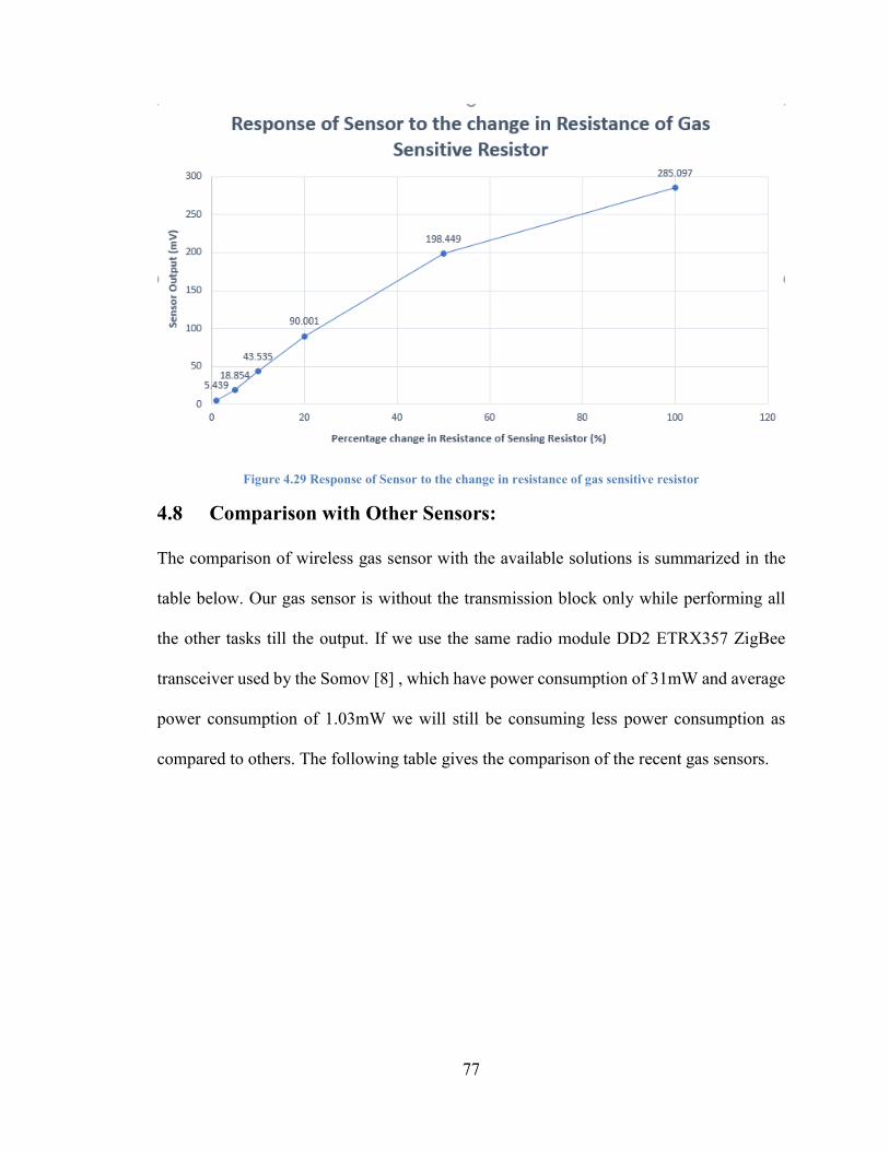
77
Figure 4.29 Response of Sensor to the change in resistance of gas sensitive resistor
4.8 Comparison with Other Sensors:
The comparison of wireless gas sensor with the available solutions is summarized in the
table below. Our gas sensor is without the transmission block only while performing all
the other tasks till the output. If we use the same radio module DD2 ETRX357 ZigBee
transceiver used by the Somov [8] , which have power consumption of 31mW and average
power consumption of 1.03mW we will still be consuming less power consumption as
compared to others. The following table gives the comparison of the recent gas sensors.

78
Table 4.5 State-of-the-art Gas Sensing Circuits: Comparative Study
Comparing with the least power consumption, The Somov [8] gas sensor has a full range
of sensitivity 30mV in Wheatstone bridge configuration and 6mV in differential
configuration when the resistance changes to full scale. With this work, the 30mV
difference is achieved with only 5% of resistance change and the full-scale change of
470mV is available with 5.06mV change with only 1% of resistance change.

79
5 CHAPTER 5
POST LAYOUT SIMULATION
The post layout simulations of the proposed Schmitt trigger, the sensor circuit based on
proposed Schmitt trigger and sensor circuit based on proposed Schmitt trigger is done in
this last chapter. This chapter outlines the layout of the proposed design and how
simulations are affected after layout extraction.
5.1 Layout for gas sensor circuit based on Schmitt Trigger based
Timer.
The layout is created in order to make the sensor universal and to be used for any gas with
the requirements suitable for any user. For this purpose, the capacitors of both sub-hertz
and 1 KHz is placed off-chip so that it can be used according to requirement of designer.
The Wheatstone bridge containing the microheaters will also be off chip and the resistors
for deciding the gain of the difference amplifier at the end will also be off chip in order to
give the flexibility to the designer to select those values according to the requirements. The
layout for the chip is shown in Figure 5.1

80
Figure 5.1 Layout for first configuration of the gas sensor (layout floorplanning)
5.2 Post Layout Simulations for both configuration of gas sensors
The post layout simulation is for the configuration is given in Figure 5.2. There is small
difference in the value of output voltage due to parasitic in connection.

81
Figure 5.2 Comparison of schematic and post-layout simulation for first configuration
The results for the post layout and schematic are compared in the table 5.2. There is small
difference due to parasitic in the connections of extracted version.
Table 5.1 Comparison for both configurations
Configurations Schematic Post-layout
1 Output (mv) 455.456 448.351

82
6 CHAPTER 6
CONCLUSION AND FUTURE WORK
In this chapter, the conclusion and inferences of the thesis are summarized. This mainly
outlines the considered problem, the proposed solution and analysis of the results. Also, a
discussion on the prospects of extending this work in future is presented at the end.
6.1 Conclusion
The purpose of this work is to design a Wireless gas sensor with lower power consumption
then the available solutions while keeping the sensitivity of the sensor. The idea was to
avoid the use of microcontroller and use the sub hertz oscillator and circuit techniques in
order to achieve the purpose of gas sensing smartly. The first objective was the reduction
of power consumption for the whole sensor which is achieved by making the circuit level
implementation of required blocks for the operation and then optimizing them to get the
required results. A new approach of integrated sensor is achieved instead of using
microcontroller and other blocks for the sensors. The next target was keeping the sensitivity
comparable while going down in power consumption. We have improved the sensitivity of
the wireless sensor by using a high gain difference amplifier at the end which uses average
power of 3.2µW but provides the gain of 63.5 which makes the output range of 470mV for
full scale variation. This allowed us to take the measurement just when the resistance starts
changing around 200°C [5] instead of going to higher temperatures. This will reduce
sufficiently the amount of power significantly as more power is lost in the heating of the
gas sensor. The average power consumption of the whole circuit is 38.77µW without the

83
micro-heater power consumption. The commercial micro-heater CCS801 by Cambridge
CMOS Sensors will consume 1mW average power for our time of operation and including
DD2 ETRX357 ZigBee transceiver block for transmission will add another 1mW average
power which will combine to give 2.072mW as overall for the whole sensor which is still
very less with the available solutions.
6.2 Future Work:
This work can be continued with the fabricating the design to make the chip of this wireless
gas sensor. Furthermore, the micro-heater with suitable materials can also be fabricated on
to the single chip to make the wireless gas sensor fully integrated. The effect of heat would
be studied and how to shield the other parts of circuit from this heat if micro-heater is
located on the same chip. After fabrication, the testing can be performed and the results
will be analyzed. With more than one wireless sensors, a wireless sensor network will be
created in order to monitor various areas of the industry. The same sensor with different
operating time can be used according to the conditions of that place. If the place has human
life working then sensors can take the measurements after a short interval of time and for
the other places like gas pipelines outside the industry, the reading time can be made
maximum in order to reduce the average power and increase the life of wireless sensor
batteries.

84
References
[1] Mohamed Hefeeda and Majid Bagheri,” Wireless Sensor Networks for Early Detection
of Forest Fires”, International Conference on Mobile Adhoc and Sensor Systems, 2007, 8-
11 Oct. 2007, Pisa, Italy, IEEE, Page(s): 1- 6
[2] Xiao Liu, Sitian Cheng, Hong Liu, Sha Hu, Daqiang Zhang and Huansheng Ning,” A
Survey on Gas Sensing Technology”, 28 Oct - 31 Oct 2012, Taipei, Taiwan, Page(s): 9635-
9665; doi:10.3390/s120709635.
[3] Stefano Tranquillini, Patrik Spieß, Florian Daniel, Stamatis Karnouskos, Fabio Casati,
Nina Oertel, Luca Mottola, Felix Jonathan Oppermann, Gian Pietro Picco, Kay Römer,
Thiemo Voigt,” Process-Based Design and Integration of Wireless Sensor Network
Applications”, Lecture Notes in Computer Science Volume 7481, 2012, Berlin, Heidelberg
pp 134-149. DOI: 10.1007/978-3-642-32885-5_10
[4] G. N. L. Ravi Teja, V. K. R. Harish, Nayeem Muddin Khan D, R. Bhargava Krishna,
Rajesh Singh, S Chaudhary,” Land Slide Detection and Monitoring System using Wireless
Sensor Networks (WSN)”, IEEE International Advance Computing Conference (IACC),
21-22 Feb. 2014, Gurgaon, India, DOI: 10.1109/IAdCC.2014.6779310.
[5] Luís M. L. Oliveira, Joel J. P. C. Rodrigues,” Wireless Sensor Networks: A Survey on
Environmental Monitoring”, Journal of Communications, VOL. 6, No. 2, April 2011.
[6] Jonathan Isaac Chanin Andrew R. Halloran,” Wireless Sensor Network for Monitoring
Applications”, A Major Qualifying Project Report Submitted to the University of
Worcester Polytechnic Institute, October 2003.

85
[7] Gang Zhao,” Wireless Sensor Networks for Industrial Process Monitoring and Control:
A Survey”, Network Protocols and Algorithms ISSN 1943-3581, Vol. 3, No. 1, 2011. DOI:
https://doi.org/10.5296/npa.v3i1.580
[8] Andrey Somov, Alexander Baranov, Denis Spirjakin, and Roberto Passerone,” Circuit
Design and Power Consumption Analysis of Wireless Gas Sensor Nodes: One-Sensor
Versus Two-Sensor Approach”, IEEE Sensors Journal, Vol. 14, NO. 6, June 2014. Page(s):
2056 – 2063 DOI: 10.1109/JSEN.2014.2309001
[9] A. Somov, A. Baranov, A. Savkin, D. Spirjakin, A. Spirjakin, and R. Passerone,
“Development of Wireless Sensor Network for Combustible Gas Monitoring,” Sens.
Actuators A, Phys., vol. 171, no. 2, pp. 398–405, Jul. 2011.
[10] Kavi K. Khedo, Rajiv Perseedoss and Avinash Mungur, “A Wireless Sensor Network
Air Pollution Monitoring System”, International Journal of Wireless and Mobile Networks
(IJWMN), Vol 2, No 2, May 2010.
[11] Jer Hayes, Stephen Beirne, King-Tong Lau, Dermot Diamond,” Evaluation of a low
cost Wireless Chemical Sensor Network for Environmental Monitoring”, IEEE Sensors,
26-29 Oct. 2008, Lecce, Italy, DOI: 10.1109/ICSENS.2008.4716494
[12] S.E. Moon, H.-K. Lee, N.-J. Choi, J. Lee, C.A. Choi, W.S. Yang, J. Kim, J.J. Jong,
D.-J. Yoo,” Low power consumption micro C2H5OH gas sensor based on micro-heater
and screen printing technique”, Sensors and Actuators B 187 (2013) Page(s): 598– 603.

86
[13] J. Hayes, S. Beirne, K.-T. Lau, and D. Diamond, “Evaluation of a low cost wireless
chemical sensor network for environmental monitoring,” in Proc. Sensors, 2008, pp. 530–
533.
[14] I.F. Akyildiz, W. Su, Y. Sankarasubramaniam, E. Cayirci,” Wireless sensor networks:
a survey” Elseveir Journal on Computer Networks Volume 38, Issue 4, 15 March 2002,
Pages 393–422.
[15] AMA association for sensor technology, Europe, “Trends in Future-Oriented Sensor
Technologies”, July 2010.
[16] Dan Chen, Zhixin Liu, Lizhe Wang, Minggang Dou, Jingying Chen, Hui Li,” Natural
Disaster Monitoring with Wireless Sensor Networks: A Case Study of Data-intensive
Applications upon Low-Cost Scalable Systems” Mobile Networks and Applications
October 2013, Springer, Volume 18, Issue 5, pp 651-663.
[17] B O’Flynn, Rafael Martínez, Català, S. Harte, C. O’Mathuna, John Cleary, C. Slater,
F. Regan, D. Diamond, Heather Murphy,” SmartCoast: A Wireless Sensor Network for
Water Quality Monitoring”, 32nd IEEE Conference on Local Computer Networks. 15-18
Oct. 2007, Dublin, Ireland, DOI: 10.1109/LCN.2007.34
[18] Liqun Hou and Neil W. Bergmann,” Novel Industrial Wireless Sensor Networks for
Machine Condition Monitoring and Fault Diagnosis”, IEEE Transactions on
Instrumentation and Measurement, Vol. 61, NO. 10, October 2012. Page(s): 2787 - 2798

87
[19] A. Somov et al., “Energy-Aware Gas Sensing Using Wireless Sensor Networks”
(Lecture Notes in Computer Science). New York, NY, USA: Springer-Verlag, 2012, pp.
245–260.
[20] S. Ho, F. Koushanfar, A. Kosterev, and F. Tittel, “LaserSPECks: Laser spectroscopic
trace-gas sensor networks-sensor integration and application,” in Proc. IPSN, 25-27 April
2007, Cambridge, MA, USA, pp. 226–235
[21] Seokhyeon Jeong, Zhiyoong Foo, Yoonmyung Lee, Jae-Yoon Sim, David Blaauw and
Dennis Sylvester,” A Fully-Integrated 71 nW CMOS Temperature Sensor for Low Power
Wireless Sensor Nodes”, IEEE Journal of Solid-State Circuits, Vol. 49, No. 8, August 2014
Page(s): 1682 – 1693.
[22] Shailesh Singh Chouhan and Kari Halonen,” A Low Power Temperature to Frequency
Converter for the On-Chip Temperature Measurement”, IEEE Sensors Journal, Vol. 15,
NO. 8, August 2015. Page(s): 4234 - 4240
[23] W. Chen, G. Liu, B. Zdravko, and A. M. Niknejad, “A highly linear broadband CMOS
LNA employing noise and distortion cancellation,” IEEE J. Solid-State Circuits, vol. 43,
no. 5, pp. 1164–1176, May 2008.
[24] Dake Wu, Ru Huang, Waisum Wong, and Yangyuan Wang, “A 0.4-V Low Noise
Amplifier Using Forward Body Bias Technology for 5 GHz Application”, IEEE
Microwave and Wireless Components Letters, Vol. 17, NO. 7, July 2007. Page(s): 543 -
545
[25] (2013). Flyport Sensing Platform [Online]. Available: http://www.openpicus.com

88
[26] Akira Shikata, Ryota Sekimoto, Tadahiro Kuroda and Hiroki Ishikuro,” A 0.5 V 1.1
MS/sec 6.3 fJ/Conversion-Step SAR-ADC With Tri-Level Comparator in 40 nm CMOS”,
IEEE Journal of Solid-State Circuits, Vol. 47, No. 4, April 2012.
[27] Poki Chen, Chun-Chi Chen, Yu-Han Peng, Kai-Ming Wang, and Yu-Shin Wang,” A
Time Domain SAR Smart Temperature Sensor with Curvature Compensation and a 3σ
Inaccuracy of 0.4 C ∼ +0.6 C Over a 0 C to 90 C Range”, IEEE Journal of Solid-State
Circuits, Vol. 45, No. 3, March 2010.
[28] Adel S. Sedra, Kenneth C. Smith “Microelectronic Circuits” Oxford Series in
Electrical & Computer Engineering, 6th Edition.
[29] Yu-Shiang Lin, Dennis Sylvester and David Blaauw,” A sub-pW timer using gate
leakage for ultra-low-power sub-Hz monitoring systems”, IEEE Custom Integrated
Circuits Conference (CICC) 16-19 Sept. 2007, San Jose, CA, USA
[30] Product brief for CCS801, Ultra-low power multi-gas sensor for indoor air quality,
Cambridge CMOS Sensors.
[31] M. Baroncini, P. Placidi, G.C. Cardinali, A. Scorzoni,” Thermal characterization of a
microheater for micromachined gas sensors”, Sensors and Actuators Volume 115, Issue 1,
15 September 2004, Pages 8–14
[32] S. Vallejos, I. Gràcia E. Figueras, J. Sánchez, R. Mas, O. Beldarrain, C. Cané,
“Microfabrication of flexible gas sensing devices based onnanostructured semiconducting
metal oxides”, Sensors and Actuators A Volume 219, 1 November 2014, Pages 88–93.

89
[33] G.Velmathi, S.Mohan , N.Ramshanker, “Importance of Temperature in Gas Sensors
and Design, Fabrication, Testing of S shaped Low Power Platinum Microheater for Gas
Sensor Applications”, International Journal of Emerging Trends in Electrical and
Electronics, Vol. 5, Issue. 2, July-2013.
[34] M. A. Khan, G. Dumstorff, C. Winkelmann, W. Lang,” Investigations on Noise Level
in AC- and DC- Bridge circuits for sensor measurement systmes”, GMA/ITG-Fachtagung
Sensoren und Messsysteme 2016
[35] C. O. Mathuna, T. O’Donnell, R. V. Martinez-Catala, J. Rohan, and B. O’Flynn,
“Energy scavenging for long-term deployable wireless sensor networks,” Talanta J., vol.
75, no. 3, pp. 613–623, May 2008.
[36] M. Cihan Çakır, Deniz Çalı¸skan , Bayram Bütün and Ekmel Özbay,” Planar Indium
Tin Oxide Heater for Improved Thermal Distribution for Metal Oxide Micromachined Gas
Sensors”, Sensors 2016
[37] Mengying Zhang, Lidong Du, Zhen Fang and Zhan Zhao,” A Sensitivity-Enhanced
Film Bulk Acoustic Resonator Gas Sensor with an Oscillator Circuit and Its Detection
Application” Micromachines 2017, 8(1), 25; doi:10.3390/mi8010025
[38] D. Wobscholl, “A wireless gas monitor with IEEE 1451 protocol,” inProc. SAS, 2006,
pp. 162–164.
[39] D. Kelaidonis et al., “Virtualization and cognitive management of real world objects
in the internet of things,” in Proc. GreenCom, 2012, pp. 187–194.

90
[40] K. Yokosawa, K. Saitoh, S. Nakano, Y. Goto, and K. Tsukada, “FET hydrogen-gas
sensor with direct heating of catalytic metal,” Sens. Actuators B, Chem., vol. 130, no. 1,
pp. 94–99, Mar. 2008.
[41] Pratchayaporn Singhanath, Apirak Suadet, Arnon Kanjanop, Thawatchai Thongleam,
Sanya Kuankid and Varakorn Kasemsuwan,” Low Voltage Adjustable CMOS Schmitt
Trigger” 4th International Conference on Modeling, Simulation and Applied Optimization
(ICMSAO), 19-21 April 2011, Kuala Lumpur, Malaysia
[42] Fei Yuan,” A high-speed differential CMOS Schmitt trigger with regenerative
current feedback and adjustable hysteresis”, Mixed Signal Letter, Analog Integrated
Circuits and Signal Process, Springer, Volume 63 Issue 1, April 2010 Pages 121 - 127
[43] Fei Yuan,” Differential CMOS Schmitt trigger with tunable hysteresis”, Express
Letter, Analog Integrated Circuits and Signal Process, Springer, Volume 62 Issue 2,
February 2010, Pages 245 – 248.
[44] Zhenhua Wang,” CMOS Adjustable Schmitt Triggers” IEEE Transactions on
Instrumentation and Measurement, vol. 40. No. 3. June 1991. Page(s): 601 - 605
[45] A. Pfister,” Novel CMOS Schmitt Trigger with Controllable Hysteresis” Electronics
Letters 26th March 1992 Vol. 28 No. 7 Page(s): 639 - 641

91
Vitae
Name :Hamza Shahid
Nationality :Pakistani
Date of Birth :8/23/1989
Email :[email protected]
Address :House No 342, Ali block, Bahria town, Lahore
Academic Background :Electrical Engineer
Publications:
[C1] Hamza Shahid, Umais Tayyab, Hussain Alzaher, “A CMOS Timer Circuit with Pulse
Width Modulation for Sub-hertz Monitoring Applications”, accepted in 14th
International MultiConference on Systems, Signals & Devices (SSD), Marrakech,
Morocco, March 2017.
[C2] Umais Tayyab, Hamza Shahid, Hussain Alzaher, “A Self-Biased Active Precision
Rectifier for Energy Harvesting Systems”, accepted in 14th International Multi-
Conference on Systems, Signals & Devices (SSD), Marrakech, Morocco, March
2017.


