NOTICE Effective October 1, 2012, QUALCOMM Incorporated completed a corporate reorganization in which the assets of certain of its businesses and groups, as well as the stock of certain of its direct and indirect subsidiaries, were contributed to Qualcomm Technologies, Inc. (QTI), a wholly- owned subsidiary of QUALCOMM Incorporated that was created for purposes of the reorganization. Qualcomm Technology Licensing (QTL), the Company’s patent licensing business, continues to be operated by QUALCOMM Incorporated, which continues to own the vast majority of the Company’s patent portfolio. Substantially all of the Company’s products and services businesses, including QCT, as well as substantially all of the Company’s engineering, research and development functions, are now operated by QTI and its direct and indirect subsidiaries 1 . Neither QTI nor any of its subsidiaries has any right, power or authority to grant any licenses or other rights under or to any patents owned by QUALCOMM Incorporated. No use of this website and/or documentation, including but not limited to the downloading of any software, programs, manuals or other materials of any kind or nature whatsoever, and no purchase or use of any products or services, grants any licenses or other rights, of any kind or nature whatsoever, under or to any patents owned by QUALCOMM Incorporated or any of its subsidiaries. A separate patent license or other similar patent-related agreement from QUALCOMM Incorporated is needed to make, have made, use, sell, import and dispose of any products or services that would infringe any patent owned by QUALCOMM Incorporated in the absence of the grant by QUALCOMM Incorporated of a patent license or other applicable rights under such patent. Any copyright notice referencing QUALCOMM Incorporated, Qualcomm Incorporated, QUALCOMM Inc., Qualcomm Inc., Qualcomm or similar designation, and which is associated with any of the products or services businesses or the engineering, research or development groups which are now operated by QTI and its direct and indirect subsidiaries, should properly reference, and shall be read to reference, QTI. 1 The products and services businesses, and the engineering, research and development groups, which are now operated by QTI and its subsidiaries include, but are not limited to, QCT, Qualcomm Mobile & Computing (QMC), Qualcomm Atheros (QCA), Qualcomm Internet Services (QIS), Qualcomm Government Technologies (QGOV), Corporate Research & Development, Qualcomm Corporate Engineering Services (QCES), Office of the Chief Technology Officer (OCTO), Office of the Chief Scientist (OCS), Corporate Technical Advisory Group, Global Market Development (GMD), Global Business Operations (GBO), Qualcomm Ventures, Qualcomm Life (QLife), Quest, Qualcomm Labs (QLabs), Snaptracs/QCS, Firethorn, Qualcomm MEMS Technologies (QMT), Pixtronix, Qualcomm Innovation Center (QuIC), Qualcomm iSkoot, Qualcomm Poole and Xiam.
Transcript
NOTICE
Effective October 1, 2012, QUALCOMM Incorporated completed a corporate reorganization in which the assets of certain of its businesses and groups, as well as the stock of certain of its direct and indirect subsidiaries, were contributed to Qualcomm Technologies, Inc. (QTI), a wholly-owned subsidiary of QUALCOMM Incorporated that was created for purposes of the reorganization.
Qualcomm Technology Licensing (QTL), the Company’s patent licensing business, continues
to be operated by QUALCOMM Incorporated, which continues to own the vast majority of the Company’s patent portfolio. Substantially all of the Company’s products and services businesses, including QCT, as well as substantially all of the Company’s engineering, research and development functions, are now operated by QTI and its direct and indirect subsidiaries1. Neither QTI nor any of its subsidiaries has any right, power or authority to grant any licenses or other rights under or to any patents owned by QUALCOMM Incorporated.
No use of this website and/or documentation, including but not limited to the downloading of
any software, programs, manuals or other materials of any kind or nature whatsoever, and no purchase or use of any products or services, grants any licenses or other rights, of any kind or nature whatsoever, under or to any patents owned by QUALCOMM Incorporated or any of its subsidiaries. A separate patent license or other similar patent-related agreement from QUALCOMM Incorporated is needed to make, have made, use, sell, import and dispose of any products or services that would infringe any patent owned by QUALCOMM Incorporated in the absence of the grant by QUALCOMM Incorporated of a patent license or other applicable rights under such patent.
Any copyright notice referencing QUALCOMM Incorporated, Qualcomm Incorporated,
QUALCOMM Inc., Qualcomm Inc., Qualcomm or similar designation, and which is associated with any of the products or services businesses or the engineering, research or development groups which are now operated by QTI and its direct and indirect subsidiaries, should properly reference, and shall be read to reference, QTI.
1 The products and services businesses, and the engineering, research and development groups, which are now operated by QTI and its subsidiaries include, but are not limited to, QCT, Qualcomm Mobile & Computing (QMC), Qualcomm Atheros (QCA), Qualcomm Internet Services (QIS), Qualcomm Government Technologies (QGOV), Corporate Research & Development, Qualcomm Corporate Engineering Services (QCES), Office of the Chief Technology Officer (OCTO), Office of the Chief Scientist (OCS), Corporate Technical Advisory Group, Global Market Development (GMD), Global Business Operations (GBO), Qualcomm Ventures, Qualcomm Life (QLife), Quest, Qualcomm Labs (QLabs), Snaptracs/QCS, Firethorn, Qualcomm MEMS Technologies (QMT), Pixtronix, Qualcomm Innovation Center (QuIC), Qualcomm iSkoot, Qualcomm Poole and Xiam.
Confidential and Proprietary - Qualcomm Atheros, Inc.
Restricted Distribution. Not to be distributed to anyone who is not an employee of either Qualcomm or a subsidiary of Qualcomm without the express approval of Qualcomm’s Configuration Management.
Not to be used, copied, reproduced in whole or in part, nor its contents revealed in any manner to others without the express written permission of Qualcomm Atheros, Inc.
QUALCOMM is a registered trademark of QUALCOMM Incorporated. ATHEROS is a registered trademark of Qualcomm Atheros, Inc. All other registered and unregistered trademarks are the property of Qualcomm Incorporated, Qualcomm Atheros, Inc. or their respective owners and used with permission. Registered marks owned by Qualcomm Incorporated and Qualcomm Atheros, Inc. are registered in the United States of America and may be registered in other countries.
This technical data may be subject to U.S. and international export, re-export, or transfer (“export”) laws. Diversion contrary to U.S. and international law is strictly prohibited.
Table RGMII DC characteristics — 1.8V I/O supply: add 2.1 to Max for symbol VIH, add GND - 0.3 to Min for symbol VIL, and add 1.9 to Max for symbol VOH
Table RGMII DC characteristics — 1.5V I/O supply: add 1.8 to Max for symbol VIH, add GND - 0.3 to Min for symbol VIL, and add 1.57 to Max for symbol VOH
Update RGMII characteristics and AC timing diagrams
MDIO timing: change Min from 10 to 0, add Typ 4, and remove Max of symbol tmdelay in Table MDIO AC characteristic
Clock characteristics: remove symbol Fs and Fo in table Recommended crystal parameters
Power pin current consumption: update the voltage range from “3.3V ±10%” to “3.3V ±5%” for symbol AVDD33 in table Power pin consumption
Revision Date Description
80-Y0618-2 Rev A 3 Confidential and Proprietary - Qualcomm Atheros, Inc.MAY CONTAIN U.S. AND INTERNATIONAL EXPORT CONTROLLED INFORMATION
AR8033 Integrated 10/100/1000 Mbps Ethernet Transceiver Data Sheet
The AR8033 Ethernet transceiver is a single port, 10/100/1000 Mbps tri-speed Ethernet PHY. The AR8033 Ethernet transceiver supports both RGMII and SGMII to the MAC. The AR8033 Ethernet transceiver belongs to the Arctic™ PHY family which provides a low power, low BOM cost solution for comprehensive applications including enterprise, carrier and home networks such as CPE, home gateway, enterprise switch, carrier switch/router, mobile base station and base station controller, optical module and media converter, industrial automation and measurement.
The AR8033 Ethernet transceiver integrates Green ETHOS® power saving technologies which significantly save power in both active operation and idle condition. Green ETHOS power saving schemes include ultra-low power in cable unplugged mode or port power down mode, as well as automatically optimized power saving based on cable length. The AR8033 Ethernet transceiver supports standard IEEE 802.3az Energy Efficient Ethernet (EEE) and Qualcomm Atheros proprietary SmartEEE™. SmartEEE allows legacy MAC and SoC devices without IEEE 802.3az support to cowork with AR8033 to provide full IEEE 802.3az support. Furthermore, the AR8033 Ethernet transceiver supports Wake-on-LAN (WoL) feature to manage and regulate total system power requirements.
The AR8033 Ethernet transceiver embeds Cable Diagnostics Test (CDT) technology for measuring cable length, detecting the cable status, and identifying remote and local PHY malfunctions, bad or marginal patch cord segments or connectors.
The AR8033 Ethernet transceiver requires only a single 3.3 V power supply. Embedded regulators are used to generate other required voltages. The AR8033 Ethernet transceiver integrates the termination circuitry at the line side.
The AR8033 Ethernet transceiver incorporates a 1.25 Gbps SerDes. This interface can be connected directly to a fiber-optic transceiver for 1000BASE-X/100BASE-FX mode or used as SGMII with MAC.
The AR8033 Ethernet transceiver supports Synchronous Ethernet by offering recovered clock output from data on the network-line side.
The AR8033 Ethernet transceiver supports IEEE 802.3az standard. The key features include:
10BASE-Te PHY uses reduced transmit amplitude.
100BASE-TX and 1000BASE-T use Low Power Idle (LPI) mode to turn off unused analog and digital blocks to save power when data traffic is idle.
1.1 Features 10BASE-Te/100BASE-TX/1000BASE-T IEEE 802.3 compliant
80-Y0618-2 Rev A 11 Confidential and Proprietary - Qualcomm Atheros, Inc.MAY CONTAIN U.S. AND INTERNATIONAL EXPORT CONTROLLED INFORMATION
AR8033 Integrated 10/100/1000 Mbps Ethernet Transceiver Data Sheet Introduction
1000BASE-T PCS and auto-negotiation with next page support
RGMII or SGMII to MAC devices
Fiber and copper combo mode when MAC interface works in RGMII mode
Additional IEEE 1000BASE-X and 100BASE-FX with integrated SerDes
RGMII timing modes support internal delay and external delay on Rx path
Green ETHOS power saving modes with internal automatic DSP power saving scheme
IEEE 802.3az EEE
SmartEEE which allows legacy MAC and SoC devices without IEEE 802.3az support to cowork with AR8033 to provide full IEEE 802.3az support
Wake-on-LAN (WoL) to detect magic packet and notify the sleeping system to wake up
Fully integrated digital adaptive equalizers, echo cancellers, and Near End Crosstalk (NEXT) cancellers
Synchronous Ethernet with frequency selectable recovered clock output
Robust Cable Discharge Event (CDE) protection of ±6 kV
Robust operation over up to 140 meters of CAT5 cable
Automatic Channel Swap (ACS)
Automatic MDI/MDIX crossover
Automatic polarity correction
IEEE 802.3u compliant auto-negotiation
Jumbo frame support up to 10 KB (full-duplex)
Multiple loopback modes for diagnostics
Robust surge protection with ±750 V/line-to-line mode and ±4 kV/line-to-ground mode IEC61000-4-5(2001)
Cable Diagnostic Test (CDT)
Single power supply: 3.3 V, optional for external regulator for core voltage
6 mm × 6 mm, 48-pin QFN package
Industry temperature (I-temp) option available
80-Y0618-2 Rev A 12 Confidential and Proprietary - Qualcomm Atheros, Inc.MAY CONTAIN U.S. AND INTERNATIONAL EXPORT CONTROLLED INFORMATION
AR8033 Integrated 10/100/1000 Mbps Ethernet Transceiver Data Sheet Introduction
1.2 Functional block diagram
DAC
Hybrid circuit
PGA
AGC
ADC
Waveshape filter
Echo canceller
Next canceller
Feed forward
equalizer
Timing and phase
recovery
Deskewer
Auto-negotiationMII management
registerDLL
Decision feedback equalizer
Symbol encoder
Symbol decoder
SGMII/SerDes
PMA
PCS
Trellis decoder Serial
interface
Sync-E
MDIOMDC
MDIO
RGMIIRGMII
80-Y0618-2 Rev A 13 Confidential and Proprietary - Qualcomm Atheros, Inc.MAY CONTAIN U.S. AND INTERNATIONAL EXPORT CONTROLLED INFORMATION
2 Pin Descriptions
This section includes a package pinout and signal descriptions.
Nomenclatures for signal names
Nomenclatures for signal types
NC No signal connection from this pin
_n Signal name suffix indicating active low signals
_P Signal name suffix indicating the positive side of a differential signal
_N Signal name suffix indicating the negative side of a differential signal
D Open drain
IA Analog input signal
I Digital input signal
I/O Digital bidirectional signal
OA Analog output signal
O Digital output signal
P Power or ground signal
PD Internal pull-down for input
PU Internal pull-up for input
80-Y0618-2 Rev A 14 Confidential and Proprietary - Qualcomm Atheros, Inc.MAY CONTAIN U.S. AND INTERNATIONAL EXPORT CONTROLLED INFORMATION
AR8033 Integrated 10/100/1000 Mbps Ethernet Transceiver Data Sheet Pin Descriptions
2.1 Pinout diagram
Figure 2-1 AR8033 48-pin QFN pinout (top view)
NOTE An exposed ground pad is on the back side of the package.
2.2 Pin descriptions
1
2
12
5
11
10
9
8
7
6
4
3
13 2423222120191817161514
48 3738394041424344454647
36
35
25
32
26
27
28
29
30
31
33
34
AR8033QFN 48-pinTop View
Exposed Ground Pad on Bottom
RSTn
LX
VDD33
MDC
INT
XTLO
XTLI
AVDDL
RBIAS
VDDH_REG
TRXP0
TRXN0
AV
DD
L
TR
XP
1
TR
XN
1
AV
DD
33
TR
XP
2
TR
XN
2
AV
DD
L
TR
XP
3
TR
XN
3
NC
LED
_AC
T
LED
_10
00
GTX_CLK
TX_EN
RX_CLK
TXD0
RX_DV
RXD0
RXD1
VDDIO_REG
RXD2
RXD3
LED_10_100
CLK_25M
MD
IO
DV
DD
L
AV
DD
L
SO
P
SO
N
SD
WO
L_IN
T
TX
D3
TX
D2
TX
D1
SIN
SIP
Table 2-1 Signal to pin descriptions
Symbol Pin Type Description
MDI
80-Y0618-2 Rev A 15 Confidential and Proprietary - Qualcomm Atheros, Inc.MAY CONTAIN U.S. AND INTERNATIONAL EXPORT CONTROLLED INFORMATION
AR8033 Integrated 10/100/1000 Mbps Ethernet Transceiver Data Sheet Pin Descriptions
TRXP0 11 IA, OA Media-dependent interface 0, differential 100 Ω transmission line
TRXN0 12
TRXP1 14 IA, OA Media-dependent interface 1, differential 100 Ω transmission line
TRXN1 15
TRXP2 17 IA, OA Media-dependent interface 2, differential 100 Ω transmission line
TRXN2 18
TRXP3 20 IA, OA Media-dependent interface 3, differential 100 Ω transmission line
TRXN3 21
RGMII
GTX_CLK 35 I, PD RGMII transmit clock, 125 MHz @ 1000 Mbps, 25 MHz @ 100 Mbps, and 2.5 MHz @ 10 Mbps digital clock input. Adding a 22 Ω damping resistor is recommended near MAC side.
RX_CLK 33 I/O, PD RGMII receive clock, 125 MHz @1000 Mbps, 25 MHz @ 100 Mbps, and 2.5 MHz @ 10 Mbps digital clock output. Adding a 22 Ω damping resistor is recommended near PHY side.
Power-on strapping input
RX_DV 32 I/O, PD RGMII receive data valid, RGMII output. Adding a 22 Ω damping resistor is recommended near PHY side.
Power-on strapping input
RXD0 31 I/O, PD RGMII receive data 0, RGMII output. Adding a 22 Ω damping resistor is recommended near PHY side.
Power-on strapping input
RXD1 30 I/O, PD RGMII receive data 1, RGMII output. Adding a 22 Ω damping resistor is recommended near PHY side.
Power-on strapping input
RXD2 28 I/O, PD RGMII receive data 2, RGMII output. Adding a 22 Ω damping resistor is recommended near PHY side.
Power-on strapping input
RXD3 27 I/O, PD RGMII receive data 3, RGMII output. Adding a 22 Ω damping resistor is recommended near PHY side.
Power-on strapping input
TX_EN 34 I, PD RGMII transmit enable, RGMII input
TXD0 36 I, PD RGMII transmit data 0, RGMII input
TXD1 37 I, PD RGMII transmit data 1, RGMII input
TXD2 38 I, PD RGMII transmit data 2, RGMII input
TXD3 39 I, PD RGMII transmit data 3, RGMII input
Table 2-1 Signal to pin descriptions (cont.)
Symbol Pin Type Description
80-Y0618-2 Rev A 16 Confidential and Proprietary - Qualcomm Atheros, Inc.MAY CONTAIN U.S. AND INTERNATIONAL EXPORT CONTROLLED INFORMATION
AR8033 Integrated 10/100/1000 Mbps Ethernet Transceiver Data Sheet Pin Descriptions
SGMII/1000BX
SIP 46 IA 1.25 Gbps transmit differential inputs
When this interface is used as a MAC interface, the MAC transmitter positive output connects to SIP and the MAC transmitter negative output connects to the SIN.
When this interface is used as a fiber interface, the fiber-optic transceiver positive output connects to the SIP and the fiber-optic transceiver negative output connects to the SIN.
SIN 45
SOP 43 OA 1.25 Gbps receive differential outputs
When this interface is used as a MAC interface, the MAC receiver positive input connects to SOP and the MAC receiver negative input connects to the SON.
When this interface is used as a fiber interface, the fiber-optic transceiver positive input connects to the SOP and the fiber-optic transceiver negative input connects to the SON.
SON 42
SD 41 IA Signal detect. 1.2 V voltage level. Input signals must not exceed 1.4 V.
High indicates that input signal is valid. Because signal detect is integrated in SerDes, this pin can be left NC.
Management interface
MDC 1 I, PU Management data clock reference
MDIO 48 I/O, D, PU
Management data, 1.5 kΩ pull-up resistor to 3.3 V/2.5 V
LED
LED_ACT 23 I/O, PU Parallel LED output for 10BASE-Te/100BASE-TX/1000BASE-T (copper) and 100BASE-X/1000BASE-X (fiber) activity; LED active based on power-on strapping.
If pulled up, active low; if pulled down, active high.
LED_1000 24 I/O, PU Parallel LED output for 1000BASE-T (copper) and 1000BASE-X (fiber) link; LED active based on power-on strapping.
If pulled up, active low; if pulled down, active high.
LED_10_100 26 I/O, PU Parallel LED output for 10BASE-Te/100BASE-TX (copper) and 100BASE-FX (fiber) link. LED active based on power-on strapping of LED_1000.
If LED_1000 is pulled up, this pin is active low; if LED_1000 is pulled down, this pin is active high.
External PUHigh 10 Mbps
Low 100 Mbps
External PDLow 10 Mbps
High 100 Mbps
For detailed information of LED, see “LED interface” on page 31.
System signal group/reference
CLK_25M 25 O Synchronous Ethernet recovered clock (25 MHz, 50 MHz, 62.5 MHz, or 125 MHz) output, frequency can be configured by register.
Table 2-1 Signal to pin descriptions (cont.)
Symbol Pin Type Description
80-Y0618-2 Rev A 17 Confidential and Proprietary - Qualcomm Atheros, Inc.MAY CONTAIN U.S. AND INTERNATIONAL EXPORT CONTROLLED INFORMATION
AR8033 Integrated 10/100/1000 Mbps Ethernet Transceiver Data Sheet Pin Descriptions
2.3 Power-on strapping
Table 2-3 lists the pin-to-PHY core power-on strapping configurations.
RSTn 2 I System reset, active low. This pin requires an external pull-up resistor to 2.5 V or 3.3 V.
XTLI 7 IA Crystal oscillator input; typical 27 pF capacitor to GND. Support external 25 MHz 1.2 V swing clock input through this pin.
XTLO 6 OA Crystal oscillator output; typical 27 pF capacitor to GND
RBIAS 9 OA External 2.37 kΩ 1% resistor to GND to set bias current
INT 5 I/O, D, PD
System interrupt output. This pin is OD-gate by default and requires external 10 kΩ pull-up resistor, active low.
WOL_INT 40 D, PD Wake-on-LAN interrupt output. This pin is OD-gate by default and requires external 10 kΩ resistor pull-up. See “Wake-on-LAN” on page 40 for details.
Power
LX 3 OA Power inductor pin. Add an external 4.7 µH/500 mA power inductor to this pin directly.
VDDH_REG 10 OA 2.5 V internal regulator output. Adding a 1 µF capacitor parallel with this pin and GND is recommended.
VDDIO_REG 29 OA Regulator output for the RGMII I/O voltage. It can be either 1.5 V (default) or 1.8 V. If 2.5 V is intended for the RGMII I/O, connect this pin with the 2.5 V regulator output at pin 10 (VDDH_REG).
AVDDL 8, 13, 19, 44
P 1.1 V analog input. Connect to pin 47 through a bead.
DVDDL 47 P 1.1 V digital core power input. Connect to power inductor directly and 10 µF+0.1 µF ceramic capacitors to GND.
VDD33 4 P 3.3 V input for internal switching regulator
AVDD33 16 P 3.3 V input for PHY, from VDD33 through a bead
In the Type column, PU and PD indicates the pin includes internal weak pull-up and pull-down resistor respectively.
Table 2-2 Not connected pin
Symbol Pin
NC 22
Table 2-1 Signal to pin descriptions (cont.)
Symbol Pin Type Description
80-Y0618-2 Rev A 18 Confidential and Proprietary - Qualcomm Atheros, Inc.MAY CONTAIN U.S. AND INTERNATIONAL EXPORT CONTROLLED INFORMATION
AR8033 Integrated 10/100/1000 Mbps Ethernet Transceiver Data Sheet Pin Descriptions
2.3.1 Mode definition
Table 2-4 lists the mode definition.
Table 2-3 Power-on strapping pins
PHY pinPHY core
configuration signalDescription
Default internal weak pull-up/down
RXD0 PHYADDRESS0 LED_ACT and RXD[1:0] set the lower three bits of the physical address. The upper two bits of the physical address are set to 00.
0
RXD1 PHYADDRESS1 0
LED_ACT PHYADDRESS2 1
RX_DV MODE[0] Mode select bit 0 0
RXD2 MODE[1] Mode select bit 1 0
RX_CLK MODE[2] Mode select bit 2 0
RXD3 MODE[3] Mode select bit 3 0
LED_1000 External interrupt select
An external 10 kΩ pull-down resistor is required.
1
1. 0 = Pull-down, 1 = Pull-up.2. Power-on strapping pins are latched during power-up reset or warm hardware reset.3. Because the MAC device input pins can be driven high or low during power-up or reset, PHY power-on
strapping status can be affected by the MAC side. In this case, an external 10 kΩ pull-down or pull-up resistor is required to ensure stable status.
Table 2-4 Mode definition
Mode [3:0] Description
0000 10BASE-Te/100BASE-TX/1000BASE-T, RGMII
0001 10BASE-Te/100BASE-TX/1000BASE-T, SGMII
0010 1000BASE-X, RGMII, 50 Ω
0011 1000BASE-X, RGMII, 75 Ω
0100 Converter mode between 1000BASE-X and 1000BASE-T media, 50 Ω
0101 Converter mode between 1000BASE-X and 1000BASE-T media, 75 Ω
0110 100BASE-FX, RGMII, 50 Ω
0111 Converter mode between 100BASE-FX and 100BASE-TX media, 50 Ω
1011 Copper/fiber auto-detection, RGMII
1110 100BASE-FX, RGMII mode, 75 Ω
1111 Converter mode between 100BASE-FX and 100BASE-TX media, 75 Ω
Others Reserved
The 50 Ω (typical) or 75 Ω is the single-ended output impedance.
80-Y0618-2 Rev A 19 Confidential and Proprietary - Qualcomm Atheros, Inc.MAY CONTAIN U.S. AND INTERNATIONAL EXPORT CONTROLLED INFORMATION
3 Function Description
The AR8033 Ethernet transceiver is an low cost GbE PHY. The highly integrated Analog Front End (AFE) and Digital Signal Processing (DSP) architecture ensures robust performance combined with substantial cost reduction. The AR8033 Ethernet transceiver provides physical layer functions for half/full-duplex 10BASE-Te, 100BASE-TX and full-duplex 1000BASE-T Ethernet to transmit and receive high-speed data over standard Category 5 (CAT5) un-shielded twisted pair cable.
The AR8033 10/100/1000 PHY is fully IEEE 802.3ab compliant, and supports Reduced Gigabit Media-Independent Interface (RGMII) to connect to a Gigabit-capable MAC.
The AR8033 Ethernet transceiver combines echo canceller, Near End Cross Talk (NEXT) canceller, feed-forward equalizer, joint Viterbi, feedback equalizer, and timing recovery, to enhance signal performance in noisy environments.
Table 3-1 lists feature comparison among the AR8031, AR8033, and AR8035 family.
Table 3-1 AR8031, AR8033, and AR8035 comparison
Feature AR8031 AR8033 AR8035
RGMII Yes Yes Yes
SGMII Yes Yes –
Cu Ethernet(2) Yes Yes Yes
EEE (IEEE 802.3az) Yes Yes Yes
Wake-on-LAN Yes Yes Yes
SerDes/Fiber(3) Yes Yes –
1588v2 Yes – –
Sync-E Yes Yes –
Packaging 48-pin 48-pin 40-pin
1. AR8031 and AR8033 are pin-to-pin compatible.2. 10BASE-Te, 100BASE-TX, and 1000BASE-T are supported.3. 100BASE-FX and 1000BASE-X are supported.
80-Y0618-2 Rev A 20 Confidential and Proprietary - Qualcomm Atheros, Inc.MAY CONTAIN U.S. AND INTERNATIONAL EXPORT CONTROLLED INFORMATION
AR8033 Integrated 10/100/1000 Mbps Ethernet Transceiver Data Sheet Function Description
3.1 Operation modes
3.1.1 Copper
Figure 3-1 shows the copper operating mode for AR8033.
Figure 3-1 Copper operating mode
SGMII is serial GMII with significantly less signal pins than required for GMII to connect with MAC/SoC. After copper-side link is established, SGMII passes the copper-side link status (link, speed, duplex) to MAC side for building the link. SGMII shares the same SerDes with the fiber port.
MAC requires to configure RGMII (including speed, duplex and pause) according to PHY link status.
The following ways can be used for MAC to get the information:
Through PHY specific status register — copper page (MII register offset 0x11)
Through interrupt function
Interrupt enable register (MII register offset 0x12) must be enabled and the interrupt status can be retrieved in Interrupt status register (MII register offset 0x13). When the controller gets the interrupt, check the interrupt source and link status in MII register 0x11.
Through inband status (RGMII)
Through auto-negotiation (SGMII)
For RGMII, by default AR8033 adds 2 ns delay for RX_CLK reference to RXD to meet the MAC input setup and hold time. The MAC to PHY direction requires to add 2 ns typical delay of GTX_CLK reference to TXD for PHY to capture the data.
3.1.2 Fiber
Figure 3-2 shows the fiber operating mode for AR8033.
MAC interface- RGMII- SGMII
Media types:- 10BASE-Te
- 100BASE-TX- 1000BASE-T
SoC or switch
RJ-45AR8033 Transformer
80-Y0618-2 Rev A 21 Confidential and Proprietary - Qualcomm Atheros, Inc.MAY CONTAIN U.S. AND INTERNATIONAL EXPORT CONTROLLED INFORMATION
AR8033 Integrated 10/100/1000 Mbps Ethernet Transceiver Data Sheet Function Description
Figure 3-2 Fiber operating mode
AR8033 supports both 1000BASE-X and 100BASE-FX modes configured by power-on strapping pins (see “Power-on strapping” on page 18) or by bits[3:0] MODE_CFG of Chip configure register. In fiber mode, the TRXP[3:0] and TRXN[3:0] pins can be left floated.
In MII registers, offset addresses (0x0, 0x1, 0x4, 0x5, 0x6, 0x7, 0x8 and 0x11) canbe used as either copper page or fiber page.
For fiber mode, set 0x1F[15] = 0 to select fiber page. Then check the link status (including link, speed, duplex and pause) in PHY specific status register — fiber page (MII register offset 0x11).
See “Copper” on page 21 for the other settings.
The fiber interface cannot auto-detect the link speed.
When set to 1000BASE-X mode, AR8033 works only in 1000 Mbps.
When set to 100BASE-FX mode, AR8033 works only in 100 Mbps.
3.1.3 Media Converter
Figure 3-3 shows the media converter operating mode for AR8033.
Figure 3-3 Media converter operating mode
AR8033
MAC interface- RGMII
Media types:- 100BASE-FX- 1000BASE-X
Fiber I/F- Serial
Fiber optics
SoC orswitch
Media types:- 100BASE-TX- 1000BASE-T
Media types:- 100BASE-FX- 1000BASE-X
Transformer RJ-45
Fiber interface: SerDes AR8033
80-Y0618-2 Rev A 22 Confidential and Proprietary - Qualcomm Atheros, Inc.MAY CONTAIN U.S. AND INTERNATIONAL EXPORT CONTROLLED INFORMATION
AR8033 Integrated 10/100/1000 Mbps Ethernet Transceiver Data Sheet Function Description
AR8033 supports the following converter modes:
100BASE-FX fiber to 100BASE-TX copper
1000BASE-X fiber to 1000BASE-T copper
The converter mode can be configured by power-on strapping pins (see “Power-on strapping” on page 18) or by bits[3:0] MODE_CFG in Chip configure register. The register configuration takes effect immediately. Three LEDs are used to indicate fiber interface status.
In converter mode, auto-negotiation is running independently on fiber and copper interfaces. The link status can be checked from copper page and fiber page respectively.
Chip configure register
Bit[15]: BT_BX_REG_SEL
– 1 = Select copper page.
– 0 = Select fiber page.
Offset addresses (0x0, 0x1, 0x4, 0x5, 0x6, 0x7, 0x8 and 0x11) can be used as either fiber page or copper page. See “Registers” on page 55 for details.
When the fiber and copper interfaces link up to the same speed, packets can go through the PHY. When 1000M converter mode (BX1000_CONV) is enabled, the copper port can still link to 100M with a 100M link partner, but packets cannot go through the PHY.
NOTE
Because the two interfaces implement auto-negotiation individually, the controller is required to ensure that the duplex and pause of two remote link partners are matched.
In converter mode, the RGMII signal can be left floated.
3.1.4 Auto-Media Detect (Combo)
AR8033 supports auto-media detect feature which allows MAC to detect active link partners and process data from copper or fiber interface according to the priority setting and link status. The copper and fiber work modes can be enabled simultaneously by setting the mode bit to 1011 by power-on strapping pin or bits[3:0] MODE_CFG in Chip configure register.
No fiber or cable connection: Both interfaces enter power saving mode.
Fiber connected: RGMII fiber mode. The PHY uses signal detection from SerDes along with the synchronization state machine to recognize a valid connection.
Copper connected: RGMII copper mode. The PHY recognizes copper connection through power transmitted over the copper line.
Combo mode: When active link partners over both fiber and copper are detected, the PHY operation mode is defined by priority setting. Priority is configured by Chip configure register:
Bit[10]: PRIORITY_SEL
– 0 = Copper
80-Y0618-2 Rev A 23 Confidential and Proprietary - Qualcomm Atheros, Inc.MAY CONTAIN U.S. AND INTERNATIONAL EXPORT CONTROLLED INFORMATION
AR8033 Integrated 10/100/1000 Mbps Ethernet Transceiver Data Sheet Function Description
– 1 = Fiber
In auto-media detect mode, fiber port can be configured to 1000BASE-X or 100BASE-FX by Chip configure register:
Bit[8]: FIBER_MODE_AUTO
1 = 1000BASE-X (default)
0 = 100BASE-FX
3.2 Transmit functions
Table 3-2 lists the transmit function encoder modes.
3.3 Receive functions
3.3.1 Decoder modes
Table 3-3 lists the receive function decoder modes.
Table 3-2 Transmit function encoder modes
Mode Description
1000BASE-T In 1000BASE-T mode, AR8033 scrambles Tx data bytes from the MAC interfaces and encodes them into 4D five-level PAM signals over the four pairs of CAT5 cable.
100BASE-TX In 100BASE-TX mode, 4-bit data from the MII is 4B/5B serialized, scrambled, and encoded to a 3-level MLT3 sequence transmitted by the PMA.
10BASE-Te In 10BASE-Te mode, AR8033 transmits and receives Manchester-encoded data.
Table 3-3 Receive function decoder mode
Mode Description
1000BASE-T In 1000BASE-T mode, the PMA recovers the 4D PAM signals after accounting for the cabling conditions such as skew among the four pairs, the pair swap order, and the polarity of the pairs. The resulting code group is decoded into 8-bit data values. Data stream delimiters are translated appropriately and data is output to the MAC interfaces.
100BASE-TX In 100BASE-TX mode, the receive data stream is recovered and descrambled to align to the symbol boundaries. The aligned data is then parallelized and 5B/4B decoded to 4-bit data. This output runs to the MII receive data pins after data stream delimiters have been translated.
10BASE-Te In 10BASE-Te mode, the recovered 10BASE-Te signal is decoded from Manchester then aligned.
80-Y0618-2 Rev A 24 Confidential and Proprietary - Qualcomm Atheros, Inc.MAY CONTAIN U.S. AND INTERNATIONAL EXPORT CONTROLLED INFORMATION
AR8033 Integrated 10/100/1000 Mbps Ethernet Transceiver Data Sheet Function Description
3.3.2 Analog-to-Digital converter
Each Rx channel includes an advanced high speed ADC with high resolution for better Signal-to-Noise Ratio (SNR) and lower error rates.
3.3.3 Echo canceller
Because hybrid circuit is used to transmit and receive simultaneously on each pair, echo occurs when the transmitter is not perfectly matched to the line. Connector or cable imperfections, such as patch panel discontinuity and variations in cable impedance along the twisted pair cable, can also result in drastic SNR degradation on the Rx signal.
The adaptive digital echo canceller is used to compensate for the varied channel conditions that result in SNR degradation on the Rx signal.
3.3.4 NEXT canceller
The 1000BASE-T physical layer uses all four twisted pairs to transmit data which incurs significant high frequency crosstalk occurs between adjacent pairs.
Three parallel NEXT cancellers are thus integrated on each Rx channel to cancel high frequency crosstalk by subtracting an estimate noise signals from the equalizer output.
3.3.5 Baseline wander canceller
Baseline wander occurs on Ethernet links AC-coupled to the transceiver. When the AC-coupling cannot maintain voltage levels for a specific time, the transmitted pulses are distorted which results in erroneous sampled values for affected pulses.
The baseline wander cancellation circuit continuously monitors and compensates for this issue, minimizing the impact of DC baseline shift on the overall error rate.
3.3.6 Digital adaptive equalizer
The digital adaptive equalizer, using a combination of Feedforward Equalizer (FFE) and Decision Feedback Equalizer (DFE), removes inter-symbol interference at the receiver by filtering unequalized signals from ADC output for optimized SNR.
3.3.7 Auto-negotiation
The auto-negotiation function for 10BASE-Te/100BASE-TX/1000BASE-T Copper complies with IEEE 802.3 clauses 28 and 40.
Auto-negotiation provides a mechanism to exchange information between a pair of link partners to choose the optimized mode of operation in terms of speed, duplex modes, and master/slave preference. Auto-negotiation is initiated upon any of the following scenarios:
Power-on reset
80-Y0618-2 Rev A 25 Confidential and Proprietary - Qualcomm Atheros, Inc.MAY CONTAIN U.S. AND INTERNATIONAL EXPORT CONTROLLED INFORMATION
AR8033 Integrated 10/100/1000 Mbps Ethernet Transceiver Data Sheet Function Description
Hardware reset
Software reset
Auto-negotiation restart
Transition from power-down to power-up
Link down
When auto-negotiation is disabled, the operation speed mode can be manually selected using the IEEE MII register 0.
NOTE In 10BASE-Te/100BASE-TX, when one end disables auto-negotiation (force mode) and the other end enables auto-negotiation (advertise half-duplex), the link can be established and the end with auto-negotiation enabled works in half-duplex mode. So if the end in force mode is in half-duplex mode, the information transmission between the two link partners works normally; if the end in force mode is in full-duplex mode, mismatch occurs between the two link partners. The link cannot be established in 1000BASE-T under similar situation.
3.3.8 Smartspeed
The Smartspeed function is an enhanced feature of auto-negotiation that allows the AR8033 device to downgrade in speed based on cabling conditions. With Smartspeed enabled, after a configurable number (MII Register 14.4:2) of failed attempts, the PHY automatically downgrades the highest ability it advertises to the next lower speed: from 1000 to 100 to 10.
The Smartspeed feature is enabled by default. See “Smart speed register” on page 85 for detailed information.
Bit[5]: SMARTSPEED_EN
1 = Enables Smartspeed (default)
0 = Disables Smartspeed
Bits[4:2]: SMARTSPEED_RETRY_LIMIT
Sets the number of link attempts before adjusting
Bit[1]: BYPASS_SMARTSPEED_TIMER
Timer to determine the stable link condition
NOTE The Smartspeed enable bit requires a software reset to take effect after writing bit[15] in Control register — copper page (0x0) to 1. When Smartspeed function is disabled, write bit[8] in Smart speed register (0x14) to 1, rather than change bit[9] in 1000BASE-T control register (0x9), to disable 1000BASE-T full-duplex link ability.
3.3.9 Automatic MDI/MDIX crossover
During auto-negotiation, the automatic MDI/MDIX crossover function automatically determines and sets the required MDI configuration, eliminating the need for external crossover cable.
80-Y0618-2 Rev A 26 Confidential and Proprietary - Qualcomm Atheros, Inc.MAY CONTAIN U.S. AND INTERNATIONAL EXPORT CONTROLLED INFORMATION
AR8033 Integrated 10/100/1000 Mbps Ethernet Transceiver Data Sheet Function Description
The algorithm described in IEEE 802.3 clause 40.4.4 ensures that only one device performs the required crossover when the remote device implements automatic MDI crossover as well.
For 1000BASE-T, swap can happen only between pair A and pair B, or pair C and pair D. See Table 3-4.
3.3.10 Polarity correction
If cable polarity is incorrectly wired, the polarity correction function automatically corrects polarity errors on the receive pairs in 1000BASE-T, 100BASE-TX, and 10BASE-Te modes.
3.4 Loopback modes
3.4.1 Digital loopback
Digital loopback loops transmitted data back to the receiver using digital circuit in the AR8033 device. Figure 3-4 and Figure 3-5 show the block diagrams for the digital loopbacks.
Figure 3-4 Digital loopback in copper mode
Figure 3-5 Digital loopback in fiber mode
Table 3-4 Supported MDI pair combinations
A (1, 2) B (3, 6) C (4, 5) D (7, 8) Normal MDI
B (3, 6) A (1, 2) D (7, 8) C (4, 5) Normal MDI-X
A (1, 2) B (3, 6) D (7, 8) C (4, 5) Normal MDI with pair swap on C and D pair
B (3, 6) A (1, 2) C (4, 5) D (7, 8) Normal MDI-X with pair swap on C and D pair
MAC/switch
RGMII/SGMII
PHY digital
PHY AFE
MAC/switch
RGMIIPHY
digitalSerDes
80-Y0618-2 Rev A 27 Confidential and Proprietary - Qualcomm Atheros, Inc.MAY CONTAIN U.S. AND INTERNATIONAL EXPORT CONTROLLED INFORMATION
AR8033 Integrated 10/100/1000 Mbps Ethernet Transceiver Data Sheet Function Description
Configuring internal loopback
MII register settings for PHY internal digital loopback mode selection:
1000M loopback: register 0x0 = 0x4140
100M loopback: register 0x0 = 0x6100
10M loopback: register 0x0 = 0x4100
3.4.2 External cable loopback
External cable loopback loops RGMII/SGMII Tx to RGMII/SGMII Rx through complete digital and analog path and an external cable. This function is used to test the digital data paths and the analog circuits. Figure 3-6 shows a block diagram of external cable loopback.
Figure 3-6 External cable loopback
Configuring external cable loopback
To configure external cable loopback:
1. Plug in an external loopback cable (1 wiring 3, 2 wiring 6, 4 wiring 7, and 5 wiring 8).
2. Set bit[15] PS_HIB_EN of External loopback selection register (Debug Register offset 0xB) to 0 to disable hibernate (power saving) mode.
3. Set bit[0] EXT_LPBK of External loopback selection register (Debug Register offset 0x11) to 1 to enable external loopback.
4. Set MII Register 0x0 to select loopback modes:
1000M loopback: register 0x0 = 0x8140
100M loopback: register 0x0 = 0xA100
10M loopback: register 0x0 = 0x8100
NOTE When cable is removed and reconnected to 1000M mode, the register 0x0 must be configured to 0x8140 again to establish PHY link.
MAC/switch
PHY digital R
J-45PHY
AFERGMII/SGMII
80-Y0618-2 Rev A 28 Confidential and Proprietary - Qualcomm Atheros, Inc.MAY CONTAIN U.S. AND INTERNATIONAL EXPORT CONTROLLED INFORMATION
AR8033 Integrated 10/100/1000 Mbps Ethernet Transceiver Data Sheet Function Description
3.4.3 Remote PHY loopback
In remote PHY loopback mode, the data from MDI Rx is looped back to MDI Tx to enable the remote link partner to detect the connectivity in the loop.
Figure 3-7 shows the block diagram of the remote PHY loopback.
Figure 3-7 Remote PHY loopback
Configuring remote PHY loopback
To enable remote PHY loopback, set bit[0] of MMD3 — RemotePHY loopback register (MMD3 Register offset 0x805A) to 1.
NOTE When remote loopback is enabled, packets from link partner still appear at RGMII.
3.5 Cable diagnostic test
The Cable Diagnostic Test (CDT) feature uses Time Domain Reflectometry (TDR) technology to identify malfunctions in remote and local PHYs, bad or marginal cable, patch cord segments and connectors.
The following are the problems that can be possibly diagnosed using CDT:
Open
Short
Cable impedance mismatch
Bad connector
Termination mismatch
Bad magnetic
The CDT can be performed when no link partner is present or the link partner is auto-negotiating.
Configuring CDT
To perform the cable diagnostic test:
MAC/switch
RGMII/SGMII
PHY digital
PHY AFE R
J-45
80-Y0618-2 Rev A 29 Confidential and Proprietary - Qualcomm Atheros, Inc.MAY CONTAIN U.S. AND INTERNATIONAL EXPORT CONTROLLED INFORMATION
AR8033 Integrated 10/100/1000 Mbps Ethernet Transceiver Data Sheet Function Description
1. Set bits[9:8] MDI PAIR SELECT of Cable diagnostic test control register (offset 0x16) to select the MDI pair to be tested.
2. Set bit[0] ENABLE TEST of Cable diagnostic test control register (offset 0x16) to 1 to enable CDT.
3. Check bits[9:8] STATUS of Cable diagnostic test status register (offset 0x1C) for cable status.
4. Check bits[7:0] DELTA_TIME of Cable diagnostic test status register (offset 0x1C) for delta time. The distance between the faulty point and PHY is [delta time] × 0.824.
3.6 Fiber mode support
Besides standard 10/100/1000 BASE-T copper port support, AR8033 provides additional IEEE 1000BASE-X and 100BASE-FX support in fiber applications through integrated SerDes. AR8033 can work in RGMII mode to fiber, 100BASE-FX to 100BASE-TX, and 1000BASE-X to 1000BASE-T.
Besides 1000BASE-X and 100BASE-FX support, AR8033 supports IEEE 802.3 remote Fault Indication and Fault Propagation in fiber application.
3.6.1 IEEE 802.3 remote fault indication support
Remote Fault allows stations on a fiber optic link to detect when a problem occurs on the link. Without Remote Fault, a station cannot detect a problem that affects only one fiber such as transmit direction fiber.
With Remote Fault, the loss of a Receive signal (Link) causes the transmitter to send a special pattern of data indicating that a fault has occurred. 84 “1”s followed by a single “0” is sent three times, in-band, and is readily detectable by the remote station. This data is constructed not to satisfy the 100BASE-X carrier sense criterion, so the message is not interpreted as normal traffic. If the remote station has Remote Fault, the link is dropped. If the remote station does not have Remote Fault, the special data pattern is ignored.
AR8033 indicates whether or not a Remote Fault pattern has been received from the remote station using the Remote Fault Status Bit. This Remote Fault Status Bit can be Propagated (see “Fault propagation” on page 30) to the copper links on both ends of a fiber link. In case of a detected fault, both ends of the link can be notified of the failure in this way. This is particularly useful given that the distances fiber links are generally used over.
3.6.2 Fault propagation
In the converter (Fiber to Copper) application, the AR8033 supports the fault propagation function. This function allows the fault in the Fiber link to be propagated to the twist-pair connection and enables both sides of PC or router to detect the link down status. With link fault propagation, system administrators can notice the link failure within a short period of time, minimizing the loss caused by this problem.
To process fault propagation for 1000BASE-X providing that the two PHYs are both AR8033 in converter mode:
80-Y0618-2 Rev A 30 Confidential and Proprietary - Qualcomm Atheros, Inc.MAY CONTAIN U.S. AND INTERNATIONAL EXPORT CONTROLLED INFORMATION
AR8033 Integrated 10/100/1000 Mbps Ethernet Transceiver Data Sheet Function Description
1. 1000BASE-X restarts auto-negotiation when the Rx path of fiber on media converter-A detects no signal or is link down.
2. If converter-A fiber keeps link down for about 40 ms, converter-A copper is shut off.
3. Because of fiber of converter-A in auto-negotiation, fiber of converter-B is also link down.
4. If converter-B fiber keeps link down for about 40 ms, converter-B copper is shut off.
To process fault propagation for the 100BASE-FX providing that the two PHYs are both AR8033 in converter mode:
1. The copper is shut off when the Rx path of fiber on media converter-A detects no signal or is link down for about 40 ms.
2. The media converter-A sends Far-End-Fault message back on Tx fiber to alert right media converter-B of link loss when the Rx path of its Fiber detects no signal or is link down.
3. The converter-B fiber is link down.
4. The copper is shut off after fiber of converter-B keeps link down for about 40 ms.
Figure 3-8 shows the Fiber Fault mechanism.
Figure 3-8 Fiber fault propagation or re-auto-negotiation
3.7 LED interface
The LED interface can be controlled by the PHY or manually, independent of the state of the PHY. The LED pins can be programmed to indicate the following status:
Operation speed
Traffic mode
Link
Figure 3-9 and Figure 3-10 show the reference designs for the LED interface.
RX
TX
TX
RX
OFF
Twisted-Pair
FiberTwisted-
PairFiber
Far-End-Fault or Re-auto negotiation
RX
TX
TX
OFF
RX
80-Y0618-2 Rev A 31 Confidential and Proprietary - Qualcomm Atheros, Inc.MAY CONTAIN U.S. AND INTERNATIONAL EXPORT CONTROLLED INFORMATION
AR8033 Integrated 10/100/1000 Mbps Ethernet Transceiver Data Sheet Function Description
Figure 3-9 Reference design for LED, active high
Figure 3-10 Reference design for LED, active low
The active status of LED_ACT and LED_1000 depends on power-on strapping mode. When the interface is strapped high, the LED interface is active low; when strapped low, the LED interface is active high.
The active status of LED_10_100 depends on LED_1000 power-on strapping mode and thus LED_10_100 and LED_1000 use the same LED reference design.
The default LED functions are listed in Table 3-5.
Table 3-5 Default LED status
Symbol 10M link 10M active 100M link 100M active 1000M link 1000M active
LED_10_100 OFF OFF ON ON OFF OFF
LED_1000 OFF OFF OFF OFF ON ON
LED_ACT ON BLINK ON BLINK ON BLINK
ON = active; OFF = inactive
10 kohm
510 ohm
470 pF
AR8033
LED_ACT
510 ohm
470 pF
AR8033
LED_ACT
VDDH_REG 3.3 V
10 kohm
80-Y0618-2 Rev A 32 Confidential and Proprietary - Qualcomm Atheros, Inc.MAY CONTAIN U.S. AND INTERNATIONAL EXPORT CONTROLLED INFORMATION
AR8033 Integrated 10/100/1000 Mbps Ethernet Transceiver Data Sheet Function Description
See Table 3-6 for LED status in RGMII to fiber mode.
NOTE In converter mode, the LEDs show the fiber port link and active status only.The LED_1000 cannot be controlled manually. The LED_ACT and LED_10_100 can be controlled by MII Registers 0x18 and 0x19.
3.8 Power supplies
One external power supply is required:
3.3 V
Internal power rails are:
3.3 V
2.5 V
1.1 V
1.8/1.5 V
AR8033 integrates a switch regulator to convert 3.3 V to 1.1 V with high efficiency for core power rail.
Two embedded LDOs are integrated to support 2.5, 1.5/1.8 V RGMII I/O voltages. When working at 2.5 V RGMII I/O, connect the VDDH_REG pin to VDDIO_REG pin directly. The 2.5 V to 1.5/1.8 V regulator can be set to any mode because the output voltage is same as input which causes regulator shutdown. When working at 2.5 V RGMII I/O, AR8033 can connect with 3.3 V RGMII I/O. Because the input can bear 3.3 V logic signal, the output logic VoH and VoL can satisfy the 3.3 V LVCMOS/LVTTL requirements. See “Electrical Characteristics” on page 43 for parameter details.
Figure 3-11 shows the reference design for 2.5/3.3 V RGMII voltage level.
Table 3-6 BaseX LED status
Symbol 100Mbps link 100Mbps active 1000Mbps link 1000Mbps active
LED_10_100 ON ON OFF OFF
LED_1000 OFF OFF ON ON
LED_ACT ON BLINK ON BLINK
ON = active; OFF = inactive
80-Y0618-2 Rev A 33 Confidential and Proprietary - Qualcomm Atheros, Inc.MAY CONTAIN U.S. AND INTERNATIONAL EXPORT CONTROLLED INFORMATION
AR8033 Integrated 10/100/1000 Mbps Ethernet Transceiver Data Sheet Function Description
Figure 3-11 Reference design, 2.5/3.3 V RGMII I/O
When working at 1.5/1.8 V RGMII I/O, disconnect VDDH_REG and VDDIO_REG and set the internal LDO to output the right voltage. The 1.5 V or 1.8 V selection is configured by bit[3] in PHY control debug register 0 (debug register 0x1F).
Figure 3-12 shows the reference design for 1.5/1.8 V RGMII voltage level.
AR8033
2.5V/3.3VRGMII
LX
VDD33
AVDDL
VDDH_REGA
VD
DL
AV
DD
33
AV
DD
L
VDDIO_REGDV
DD
L
1uF
0.1uF
0.1uF
0.1uF
0.1uF
3.3 V input
Bead
Bead
0.1uF4.7uH
0.1uF
0.1uF10uF
10uF 0.1uF
1uF
AV
DD
L
0.1uF
80-Y0618-2 Rev A 34 Confidential and Proprietary - Qualcomm Atheros, Inc.MAY CONTAIN U.S. AND INTERNATIONAL EXPORT CONTROLLED INFORMATION
AR8033 Integrated 10/100/1000 Mbps Ethernet Transceiver Data Sheet Function Description
Figure 3-12 Reference design, 1.5/1.8 V RGMII I/O
3.9 Management interface
The management interface, compliance with IEEE 802.3u clause 22, provides access to the internal registers of PHYs via the MDC and MDIO pins. MDC is sourced by the station management entity to the PHY as the timing reference for transfer of information on the MDIO signal.
MDIO is a bidirectional signal between the PHY and the STA. It is used to transfer control information and status between the PHY and the STA. Control information is driven by the STA synchronously with respect to MDC and is sampled synchronously by the PHY. Status information is driven by the PHY synchronously with respect to MDC and is sampled synchronously by the STA.
MDIO is an open-drain I/O and requires an external 1.5 kΩ pull-up resistor.
Table 3-7 and Table 3-8 describe the management interface format.
AR8033
1.5/1.8VRGMII
LX
VDD33
AVDDL
VDDH_REGA
VD
DL
AV
DD
33
AV
DD
L
VDDIO_REGDV
DD
L
0.1uF
0.1uF
0.1uF
0.1uF
0.1uF
3.3 V input
Bead
Bead
0.1uF4.7uH
0.1uF
1uF10uF
10 uF0.1uF
1uF
AV
DD
L
0.1uF
Table 3-7 Management interface frame fields
PRE ST OP PHYAD REGAD TA DATA IDLE
80-Y0618-2 Rev A 35 Confidential and Proprietary - Qualcomm Atheros, Inc.MAY CONTAIN U.S. AND INTERNATIONAL EXPORT CONTROLLED INFORMATION
AR8033 Integrated 10/100/1000 Mbps Ethernet Transceiver Data Sheet Function Description
3.10 Timing synchronization
3.10.1 Synchronous Ethernet
Synchronous Ethernet (Sync-E) is a timing synchronization method implemented at the physical layer.
The AR8033 transceiver supports synchronous Ethernet for 100BASE-TX and 1000BASE-T applications by offering one recovered clock from the network line-side. This recovered clock output (CLK_25M) can be configured to 25 MHz (default), 50 MHz, 62.5 MHz or 125 MHz, to meet the ITU-T recommendations G.8261/Y.1361. The network node can use this recovered clock to replace local clock sources and drive the local system. Therefore all distributed nodes in the system use the same network clock to support synchronous and timing sensitive services like T1/E1 service over Ethernet.
CLK_25M
Figure 3-13 shows the CLK_25M in reference to power-up and reset timing.
READ 1...1 01 10 AAAAA RRRRR Z0 DDDDDDDDDDDDDDDD Z
WRITE 1...1 01 01 AAAAA RRRRR 10 DDDDDDDDDDDDDDDD Z
Table 3-8 Management interface field definitions
Field Definition
PRE A sequence of 32 contiguous single logic bits on MDIO with corresponding cycles on MDC to provide PHY with a pattern for synchronization.
PHYAD 5-bit PHY device address. The bits[2:0] in the PHY address are configured by power-on strapping, thus eight PHYs can be connected to a single management interface. The PHYs connected to the same bus have unique PHY addresses. The first PHY address bit transmitted and received is the MSB of the address.
REGAD 5-bit register address. The 5-bit register address allows 32 registers to be addressed at each PHY. The first register address bit transmitted and received is the MSB of the address.
TA 2-bit field to avoid contention during a read operation.
In read operation, both MAC and PHY are at high-impedance state for the first bit time. The PHY drives a zero during the second bit time of the turnaround.
In write operation, the MAC must drive 10.
DATA 16-bit data from accessed register. MSB is transmitted first.
IDLE High-impedance without driving state of the MDIO. At least one clocked idle state is required between frames.
80-Y0618-2 Rev A 36 Confidential and Proprietary - Qualcomm Atheros, Inc.MAY CONTAIN U.S. AND INTERNATIONAL EXPORT CONTROLLED INFORMATION
AR8033 Integrated 10/100/1000 Mbps Ethernet Transceiver Data Sheet Function Description
Figure 3-13 CLK_25M timing
When power is stable, CLK_25M is stable in 5 ms.
CLK_25M can output clock for system application. If not used, it can be left floated.
If used in synchronous Ethernet, CLK_25M is divided from the DSP clock recovered from the line side; if not used in synchronous Ethernet or linked down, the 50, 62.5, or 125 MHz clock is divided from PLL that references the local clock; the 25 MHz clock is from oscillator directly not from PLL.
If CLK_25M output is used as a stable system reference, configure AR8033 to PLL ON mode by setting bit[2] to 1 in PHY control debug register 0 (debug register 0x1F). In PLL OFF mode, when entering hibernation mode, AR8033 shuts down internal PLL and thus causes CLK_25M output to drop periodically. The 25 MHz clock does not drop periodically.
CLK_25M outputs 25 MHz clock from local crystal by default. When CLK_25 is configured to output 50, 62.5 or 125 MHz clock, the output is reset to default 25 MHz after hardware reset.
See “MMD7 — CLK_25M clock select register” on page 108 for details.
In RGMII to fiber (1000BASE-X/100BASE-FX) mode, PHY recovers clock from received data. This recovered clock is sent out from the RX_CLK pin. The RX_CLK pin can be used as Sync-E recovered clock that is synchronous with the link partner output reference clock.
In 1000BASE-X mode, RX_CLK outputs 125 MHz; in 100BASE-FX mode, RX_CLK outputs 25 MHz.
NOTE Clear to default value on hardware reset. If the fiber interface SerDes is not getting any valid energy for about ten seconds, AR8033 enters hibernation mode (power saving mode). In hibernation mode, RX_CLK is turned off. To enable RX_CLK to always output valid clock, write MMD7 Register 0x8005[15] = 0 to turn off SerDes hibernation mode.
< 5ms CLK_25M
3.3V
Reset
80-Y0618-2 Rev A 37 Confidential and Proprietary - Qualcomm Atheros, Inc.MAY CONTAIN U.S. AND INTERNATIONAL EXPORT CONTROLLED INFORMATION
AR8033 Integrated 10/100/1000 Mbps Ethernet Transceiver Data Sheet Function Description
3.11 Green ETHOS feature
3.11.1 Low power modes
The AR8033 device supports the low power mode with software power-down.
To enter the standard IEEE power-down mode, set the bit[11] POWER_DOWN of Control register — copper page or Control register — fiber page to 1. In this mode, AR8033 ignores all MAC interface signals except the MDC/MDIO and does not respond to any activity on the media side.
AR8033 cannot wake up on its own and is only waken up by setting the POWER_DOWN bit to 0.
3.11.2 Short cable power mode
Given cable length of less than 30 meters, Qualcomm Atheros proprietary Green ETHOS power saving technology saves 25% power consumption over standard consumption on 100-meter CAT5 cable.
3.11.3 Hibernation mode
Hibernation mode yields very low power consumption compared with normal operation mode.
When cable is unplugged, AR8033 enters hibernation mode in about 10 seconds. When cable is reconnected, AR8033 wakes up to restore normal function.
3.12 IEEE 802.3az
IEEE 802.3az provides a mechanism to reduce power consumption between data packets bursts. Two operating states are supported: active state for normal data transfer, and Low Power Idle (LPI) state for power saving between the data packet bursts.
The link partners enter LPI state by sending short refresh signals to maintain the link. In the low-power state, PHY shuts down most of the analog and digital blocks. In Ethernet network where systems stay in non-burst mode most of time, therefore over 90% power can be saved with LPI enabled.
During link establishment, both link partners exchange information through auto-negotiation to determine if both parties are LPI-capable.
Legacy Ethernet products are supported.
The link states for IEEE 802.3az include:
Active: Act in regular mode for transmitting or receiving data.
Sleep: Send specific signal to inform remote link partner of entering low-power state.
Quiet: No signal transmitted on media. Most of the analog and digital blocks are shut down.
80-Y0618-2 Rev A 38 Confidential and Proprietary - Qualcomm Atheros, Inc.MAY CONTAIN U.S. AND INTERNATIONAL EXPORT CONTROLLED INFORMATION
AR8033 Integrated 10/100/1000 Mbps Ethernet Transceiver Data Sheet Function Description
Refresh: Periodically send specific training signal to maintain timing recovery and equalizer coefficients.
Wake: Send specific wake-up signal to remote link partner to inform of entering Active state.
IEEE 802.3az LPI is supported on 100BASE-TX and 1000BASE-T.
100BASE-TX EEE allows asymmetrical operation that allows Tx or Rx to enter the LPI mode independently.
1000BASE-T EEE requires symmetrical operation that both Tx and Rx must enter the LPI mode simultaneously.
Figure 3-14 shows the IEEE 802.3az operating states for AR8033.
Figure 3-14 Operating states — 802.3az LPI mode
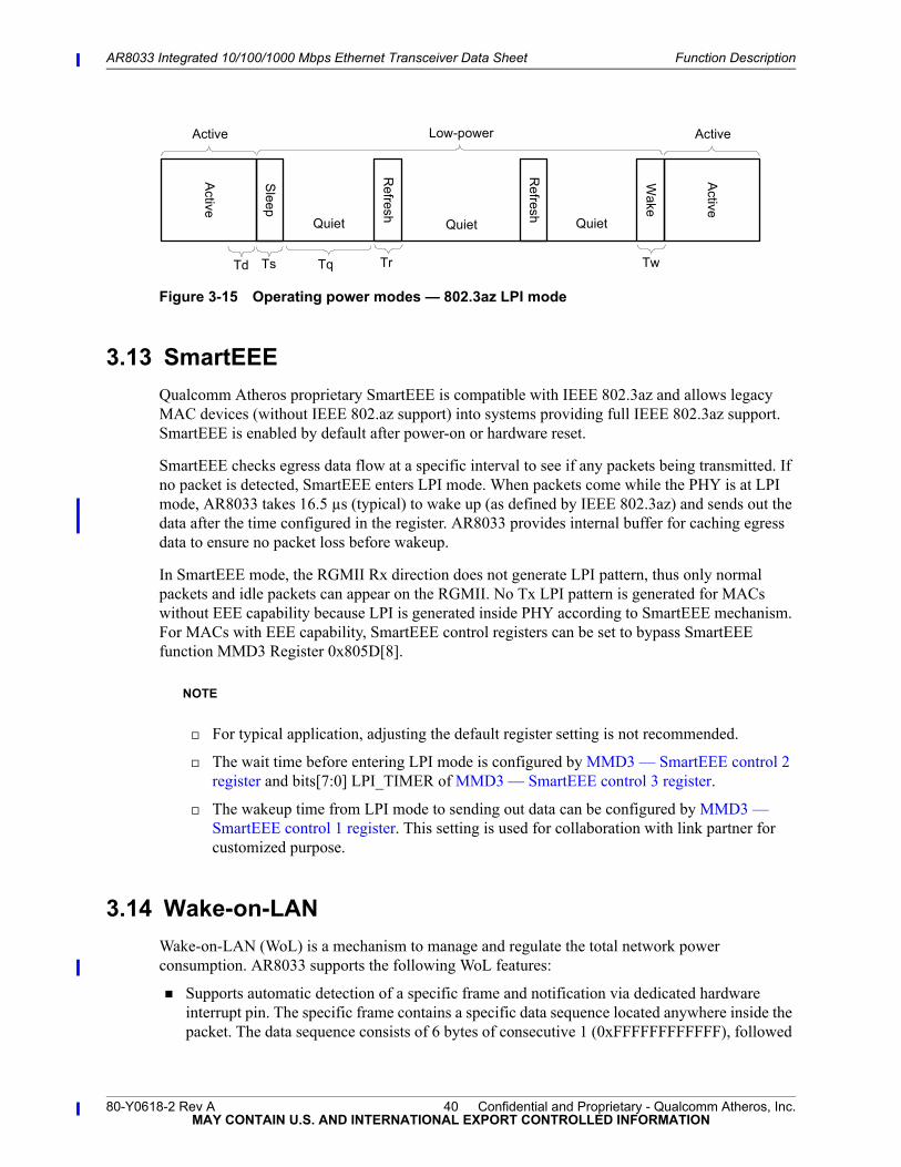
Figure 3-15 shows the IEEE 802.3az operating power modes for AR8033.
Active
Active
Td
Existing state used for data transmission. Data packets or IPG/Idle symbols are transmitted
New state used during periods of no data transmission to allow system power reduction
between data packet bursts
Operating states
Sleep
Refresh
Refresh
Quiet
Wa
ke
Quiet Quiet
Low-power
TrTqTs Tw
Td: Decision time, higher-layer control policy timingTs: Sleep time, Min. duration Sleep symbols sent before going to QuietTq: Quiet duration, Max. duration PHY remains Quiet before RefreshTr: Refresh duration, Min. duration HY sends Refresh symbolsTw: Wake time, Max. period to permit the receiving system to wake up
80-Y0618-2 Rev A 39 Confidential and Proprietary - Qualcomm Atheros, Inc.MAY CONTAIN U.S. AND INTERNATIONAL EXPORT CONTROLLED INFORMATION
AR8033 Integrated 10/100/1000 Mbps Ethernet Transceiver Data Sheet Function Description
Figure 3-15 Operating power modes — 802.3az LPI mode
3.13 SmartEEE
Qualcomm Atheros proprietary SmartEEE is compatible with IEEE 802.3az and allows legacy MAC devices (without IEEE 802.az support) into systems providing full IEEE 802.3az support. SmartEEE is enabled by default after power-on or hardware reset.
SmartEEE checks egress data flow at a specific interval to see if any packets being transmitted. If no packet is detected, SmartEEE enters LPI mode. When packets come while the PHY is at LPI mode, AR8033 takes 16.5 µs (typical) to wake up (as defined by IEEE 802.3az) and sends out the data after the time configured in the register. AR8033 provides internal buffer for caching egress data to ensure no packet loss before wakeup.
In SmartEEE mode, the RGMII Rx direction does not generate LPI pattern, thus only normal packets and idle packets can appear on the RGMII. No Tx LPI pattern is generated for MACs without EEE capability because LPI is generated inside PHY according to SmartEEE mechanism. For MACs with EEE capability, SmartEEE control registers can be set to bypass SmartEEE function MMD3 Register 0x805D[8].
NOTE
For typical application, adjusting the default register setting is not recommended.
The wait time before entering LPI mode is configured by MMD3 — SmartEEE control 2 register and bits[7:0] LPI_TIMER of MMD3 — SmartEEE control 3 register.
The wakeup time from LPI mode to sending out data can be configured by MMD3 — SmartEEE control 1 register. This setting is used for collaboration with link partner for customized purpose.
3.14 Wake-on-LAN
Wake-on-LAN (WoL) is a mechanism to manage and regulate the total network power consumption. AR8033 supports the following WoL features:
Supports automatic detection of a specific frame and notification via dedicated hardware interrupt pin. The specific frame contains a specific data sequence located anywhere inside the packet. The data sequence consists of 6 bytes of consecutive 1 (0xFFFFFFFFFFFF), followed
Active
Active
Sleep
Refresh
Refresh
Quiet
Wake
Quiet Quiet
Low-power
Ts Tq TrTd
Active
Active
Tw
80-Y0618-2 Rev A 40 Confidential and Proprietary - Qualcomm Atheros, Inc.MAY CONTAIN U.S. AND INTERNATIONAL EXPORT CONTROLLED INFORMATION
AR8033 Integrated 10/100/1000 Mbps Ethernet Transceiver Data Sheet Function Description
by 16 repetitions of the MAC address of the computer to be waken up. The 48-bit MAC address is written in MMD3 0x804A, 0x804B, 0x804C registers.
For example, to write a specific MAC address (0xAAAABBBBCCCC) to PHY, write MMD3 0x804A = 0xAAAA, 0x804B = 0xBBBB, and 0x804C = 0xCCCC. The PHY internal MAC address can be set to any value.
NOTE The MAC address is not a real MAC address and is only a symbol to indicate the content of the frame.
Figure 3-16 shows the WoL system application structure.
Figure 3-16 WoL system application structure
Two hardware pins can be used for triggering WoL interrupt:
Active low signal through the INT pin. When the interrupt bit in register 0x12[0] is set to 1, AR8033 generates interrupt at the reception of WoL packet.
Active with pulse width of 32 clock cycles through the WOL_INT pin at the reception of WoL packet. Clock frequencies for different traffic rates are:
– 1000 Mbps: 125 MHz
– 100 Mbps: 25 MHz
– 10 Mbps: 2.5 MHz
For example, if the link speed is 1000 Mbps, the clock frequency is 125 MHz and the clock cycle is 8 ns, the WoL is active with a 32 × 8 ns low pulse.
When WoL interrupt occurs, the bit[0] INT_WOL_PTP in Interrupt status register (MII Register 0x13) is set to 1. This bit is cleared after read operation.
When the bit[0] INT_WOL_PTP in Interrupt enable register is set to 1, the external INT pin is triggered when interrupt occurs. When the bit[0] INT_WOL_PTP is cleared to 0, the external INT pin cannot be triggered even when interrupt occurs.
NOTE
ARCTICPHY
ControllerWOL_INT
INT
Written MAC address
MDC/MDIO
FF FF FF FF FF FF MAC address
Fiber/copper
>=16*MAC address
Same address
80-Y0618-2 Rev A 41 Confidential and Proprietary - Qualcomm Atheros, Inc.MAY CONTAIN U.S. AND INTERNATIONAL EXPORT CONTROLLED INFORMATION
AR8033 Integrated 10/100/1000 Mbps Ethernet Transceiver Data Sheet Function Description
Because PHY requires to receive packets from the line side, PHY cannot be powered down. If the link partner supports Energy Efficient Ethernet function, both ends can use EEE mode to save more power.
In LPI mode, the controller can use WoL function to turn off unused circuits to save power. When receiving WoL interrupt from PHY, the controller can wake up to work.
– Control register — copper page or Control register — fiber page (MII Register 0x0)
• Bit[10] ISOLATE: When this bit is set to 1, the RGMII output pins are tri-stated. The RGMII inputs are ignored. This bit can be used to save more power of PHY in system power saving mode. When receiving WoL packet, this bit is cleared automatically.
The bit[5] WOL_EN in MMD3 — PTP1588 control register (MMD3 0x8012) is used to enable or disable WoL function.
Programming INT work mode and active polarity
1. Power on by default configuration.
If INT is configured as interrupt function by power-on strapping (LED_1000 externally pulled-down), INT is active low.
If LED_1000 is pulled-up, write MMD7 0x8016[12] = 1 to enable the interrupt function for the INT pin.
2. Select INT polarity.
Write MMD7 0x801A[13] = 0 to set interrupt active high (by default the value is 1, active low).
80-Y0618-2 Rev A 42 Confidential and Proprietary - Qualcomm Atheros, Inc.MAY CONTAIN U.S. AND INTERNATIONAL EXPORT CONTROLLED INFORMATION
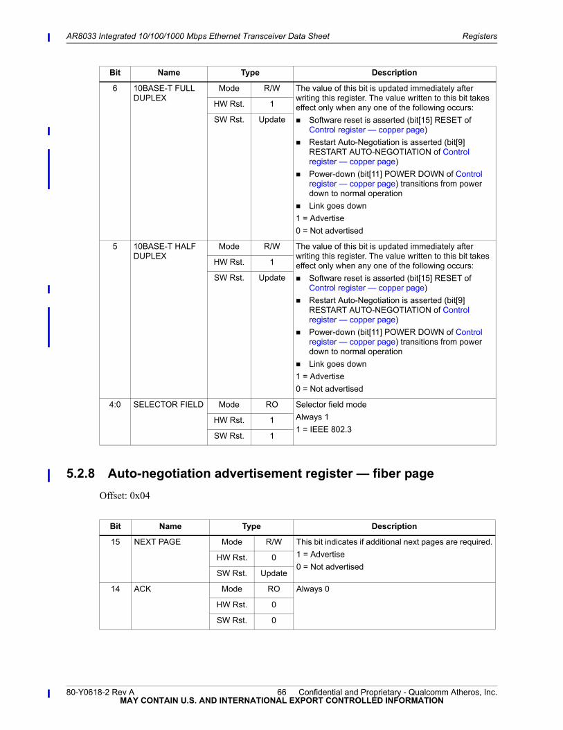
4 Electrical Characteristics
4.1 Absolute maximum ratings
Table 4-1 summarizes the absolute maximum ratings for the AR8033 Ethernet transceiver. Absolute maximum ratings are those values beyond which damage to the device can occur. Functional operation under these conditions, or at any other condition beyond those indicated in the operational sections of this document, is not recommended.
4.2 Recommended operating conditions
Table 4-2 lists the recommended operating conditions for the AR8033 Ethernet transceiver.
Table 4-1 Absolute maximum ratings
Symbol Parameter Max rating Unit
VDD33/AVDD33 3.3 V supply voltage 3.8 V
AVDDL 1.1 V analog supply voltage 1.6 V
DVDDL 1.1 V digital core supply voltage 1.6 V
Tstore Storage temperature -65 to 150 °C
HBM Electrostatic discharge tolerance — human body model ±2000 V
MM Machine model ±200 V
Vmin Supply voltage min -0.3 V
Table 4-2 Recommended operating conditions
Symbol Parameter Min Typ Max Unit
VDD33/AVDD33 3.3 V supply voltage 3.15 3.3 3.45 V
VDDH_REG 2.5 V analog/digital 2.4 2.62 2.75 V
AVDDL/DVDDL 1.1 V analog/digital with on-chip regulator
1.04 1.1 1.17 V
Tambient Ambient temperature for normal operation — Commercial chip version AR8033-AL1A
0 – 70 °C
Ambient temperature for normal operation — Industrial chip version AR8033-AL1B
-40 – 85 °C
80-Y0618-2 Rev A 43 Confidential and Proprietary - Qualcomm Atheros, Inc.MAY CONTAIN U.S. AND INTERNATIONAL EXPORT CONTROLLED INFORMATION
AR8033 Integrated 10/100/1000 Mbps Ethernet Transceiver Data Sheet Electrical Characteristics
NOTE External regulators are optional for supplying AVDDL/DVDDL. For industrial version, external AVDDL/DVDDL inputs must be within the range of 1.2 V ± 5%. For commercial version, external AVDDL/DVDDL inputs must be within the range of 1.1 V - 5% and 1.2 V + 5%.
NOTE The following condition must be satisfied:
TJmax > TCmax + ΨJT × PTypical
Where:
TJmax = Maximum allowable junction temperature
TCmax = Maximum allowable case temperature
ΨJT = Thermal dissipation coefficient
PTypical = Typical power dissipation
4.3 RGMII characteristics
Table 4-3 shows the RGMII DC characteristics with 2.5/3.3V I/O supply.
Table 4-4 shows the RGMII DC characteristics with 1.8 V I/O supply.
Table 4-3 RGMII DC characteristics — 2.5/3.3V I/O supply
Symbol Parameter Min Max Unit
IIH Input high current – 15 μA
IIL Input low current -15 – μA
VIH Input high voltage 1.7 3.5 V
VIL Input low voltage GND - 0.3 0.7 V
VOH Output high voltage 2.4 2.8 V
VOL Output low voltage GND - 0.3 0.4 V
Table 4-4 RGMII DC characteristics — 1.8V I/O supply
Symbol Parameter Min Max Unit
VIH Input high voltage 1.4 2.1 V
VIL Input low voltage GND - 0.3 0.4 V
80-Y0618-2 Rev A 44 Confidential and Proprietary - Qualcomm Atheros, Inc.MAY CONTAIN U.S. AND INTERNATIONAL EXPORT CONTROLLED INFORMATION
AR8033 Integrated 10/100/1000 Mbps Ethernet Transceiver Data Sheet Electrical Characteristics
Table 4-5 shows the RGMII DC characteristics with 1.5 V I/O supply.
Figure 4-1 shows the RGMII input AC timing diagram.
Figure 4-1 RGMII input timing diagram
Table 4-6 shows the RGMII input AC characteristics.
RX_CLK hardware reset adds typical 2 ns delay internally by default, so the MAC side has sufficient setup and hold time for sampling. Figure 4-2 shows the RGMII output AC timing with internal delay added diagram.
VOH Output high voltage 1.5 1.9 V
VOL Output low voltage – 0.3 V
Table 4-5 RGMII DC characteristics — 1.5 I/O supply
Symbol Parameter Min Max Unit
VIH Input high voltage 1.2 1.8 V
VIL Input low voltage GND - 0.3 0.3 V
VOH Output high voltage 1.3 1.57 V
VOL Output low voltage – 0.2 V
Table 4-6 RGMII AC characteristics — no internal delay
Symbol Parameter Min Typ Max Unit
TsetupR Data to clock input setup time (at receiver) 1.0 2.0 – ns
TholdR Data to clock input hold time (at receiver) 1.0 2.0 – ns
1. If the transmitter side (MAC) does not add internal delay or PCB trace delay for GTX_CLK, the input setup and hold time minimum must be within ±0.5 ns. GTX_CLK precise 2.4 ns delay can be added in PHY internal by setting bit[8] RGMII_TX_CLK_DLY = 1 in SerDes test and system mode control register (Debug Register 0x5).
2. For 1000BASE-T, both the rising and falling edges are used to sample the data.3. For 10BASE-Te/100BASE-TX, only the rising edge is used to sample the data.
Table 4-4 RGMII DC characteristics — 1.8V I/O supply (cont.)
TXD[3:0], TX_EN
TholdRGTX_CLK
TsetupRTsetupR
TholdR
80-Y0618-2 Rev A 45 Confidential and Proprietary - Qualcomm Atheros, Inc.MAY CONTAIN U.S. AND INTERNATIONAL EXPORT CONTROLLED INFORMATION
AR8033 Integrated 10/100/1000 Mbps Ethernet Transceiver Data Sheet Electrical Characteristics
Figure 4-2 RGMII output AC timing diagram with internal delay added
Table 4-7 shows the RGMII AC characteristics with delay added.
4.4 SerDes and SGMII characteristics
Table 4-8 shows the Driver DC characteristics.
Table 4-7 RGMII AC characteristics — with internal delay added (default)
Symbol Parameter Min Typ Max Unit
TsetupT Data to clock output setup (at transmitter — integrated delay)
1.2 2.0 – ns
TholdT Clock to data output hold (at transmitter — integrated delay)
1.2 2.0 – ns
1. RX_CLK delay can be disabled by setting bit[15] SEL_CLK125M_DSP = 0 in Analog test control register (Debug Register 0x0).
2. If RX_CLK delay is disabled in PHY, the RX_CLK to RXD edge delay is within ±500 ps requiring the MAC side to add internal delay or PCB trace delay.
RX_CLK
RXD[3:0], RX_DV TsetupT
RXC with internal delay added
TholdR
Table 4-8 Driver DC characteristics
Symbol Parameter Min Typical Max Unit
Voh Output voltage high – 950 1050 mV
Vol Output voltage low 500 650 – mV
Vring Output ringing – – 10 %
|Vod| Output differential voltage Programmable
300 (default)
mV
Vos Output offset voltage 750 800 850 mV
Ro Output impedance
(single-ended)
50ohm termination
40 50 60 ohm
Output impedance
(single-ended)
75ohm termination
60 75 90 ohm
Delta Ro Mismatch in a pair – – 10 %
Delta VOD Change in VOD between “0” and “1” – – 25 mV
80-Y0618-2 Rev A 46 Confidential and Proprietary - Qualcomm Atheros, Inc.MAY CONTAIN U.S. AND INTERNATIONAL EXPORT CONTROLLED INFORMATION
AR8033 Integrated 10/100/1000 Mbps Ethernet Transceiver Data Sheet Electrical Characteristics
Table 4-9 shows the Receiver DC characteristics
Table 4-10 shows the Driver AC characteristics.
4.5 MDIO timing
Figure 4-3 shows the MDIO AC timing diagram.
Delta Vos Change in VOS between “0” and “1” – – 25 mV
Isa,Isb Output current on short to GND – – 40 mA
Isab Output current when a, b are shorted – – 12 mA
Ixa,Ixb Power off leakage current – – 10 mA
Output differential voltage can be configured by register MMD7 0x8011 [15:13].
Table 4-9 Receiver DC characteristics
Symbol Parameter Min Typical Max Unit
Vio Internal offset voltage 730 825 930 mV
Vih Input single voltage high – 1050 1150 mV
Vil Input single voltage low 500 600 – mV
Vidth Input differential threshold -50 – +50 mV
Vhyst Input differential hysteresis 25 – – mV
Rin Receiver differential input impedance
50ohm termination
80 100 120 ohm
Receiver differential input impedance
75ohm termination
120 150 180 ohm
Table 4-10 Driver AC characteristics
Symbol Parameter Min Max Unit
tfall Vod fall time
(20%-80%)
100 200 ps
trise Vod rise time
(20%-80%)
100 200 ps
Tskew1 Skew between two members of a differential pair
– 20 ps
Skew measured at 50% of the transition.
Table 4-8 Driver DC characteristics (cont.)
Symbol Parameter Min Typical Max Unit
80-Y0618-2 Rev A 47 Confidential and Proprietary - Qualcomm Atheros, Inc.MAY CONTAIN U.S. AND INTERNATIONAL EXPORT CONTROLLED INFORMATION
AR8033 Integrated 10/100/1000 Mbps Ethernet Transceiver Data Sheet Electrical Characteristics
Figure 4-3 MDIO AC timing diagram
4.6 MDIO/MDC DC characteristic
Table 4-11 MDIO AC characteristic
Symbol Parameter Min Typ Max Unit
tmdc MDC period 40 – – ns
tmdcl MDC low period 16 – – ns
tmdch MDC high period 16 – – ns
tmdsu MDIO to MDC rising setup time 10 – – ns
tmdhold MDIO to MDC rising hold time 10 – – ns
tmdelay MDC to MDIO output delay 0 4 – ns
MDC
tmdhold
VIH
VIL
VIH
VIL
tmdsu
tmdcltmdch
tmdc
MDIO
Table 4-12 MDIO/MDC DC characteristic
Symbol Parameter Min Max Unit
VOH Output high voltage 2.4 – V
VOL Output low voltage – 0.4 V
VIH Input high voltage 1.7 – V
VIL Input low voltage – 0.7 V
IIH Input high current – 0.4 mA
IIL Input low current -0.4 – mA
80-Y0618-2 Rev A 48 Confidential and Proprietary - Qualcomm Atheros, Inc.MAY CONTAIN U.S. AND INTERNATIONAL EXPORT CONTROLLED INFORMATION
AR8033 Integrated 10/100/1000 Mbps Ethernet Transceiver Data Sheet Electrical Characteristics
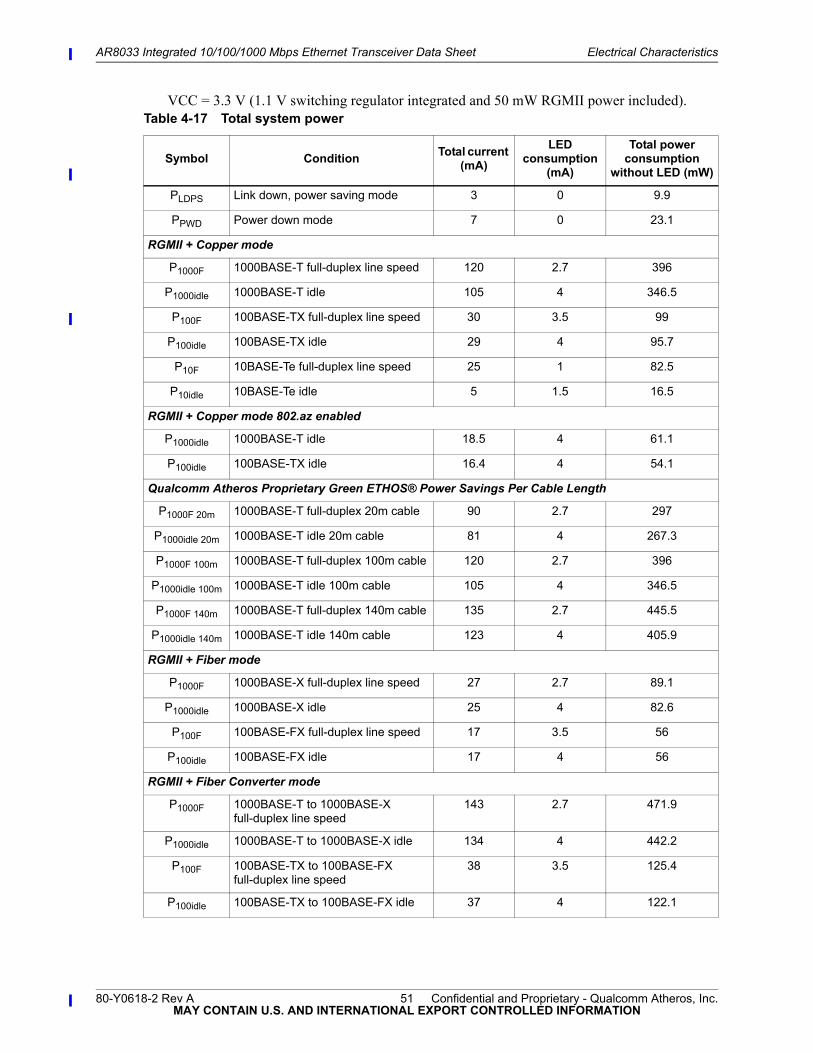
4.7 Clock characteristics
AR8033 supports both crystal and external clock input as reference. The basic principle for selecting crystal and load capacitance is to make the oscillation stable at 25 MHz ± 50 ppm. Crystal with 25 MHz ± 30 ppm frequency tolerance is preferred with two 27 pF NPO ceramic capacitors. The capacitors can be changed according to actual crystal selection and board level test results under full application temperature and voltage ranges.
Figure 4-4 External crystal
Table 4-13 Recommended crystal parameters
Symbol Parameter Min Typ Max Unit
Ff Crystal fundamental frequency – 25 – MHz
Ft Frequency tolerance -30ppm – +30ppm MHz
Cs Shunt capacitance – 7 – pF
Cl Load capacitance – 15 – pF
Vo I/O voltage level (for drive level evaluation) – 1.2 – V
DL Drive level – 300 – µW
ESR Equivalent series resistance – 30 50 Ω
Table 4-14 External clock input characteristic
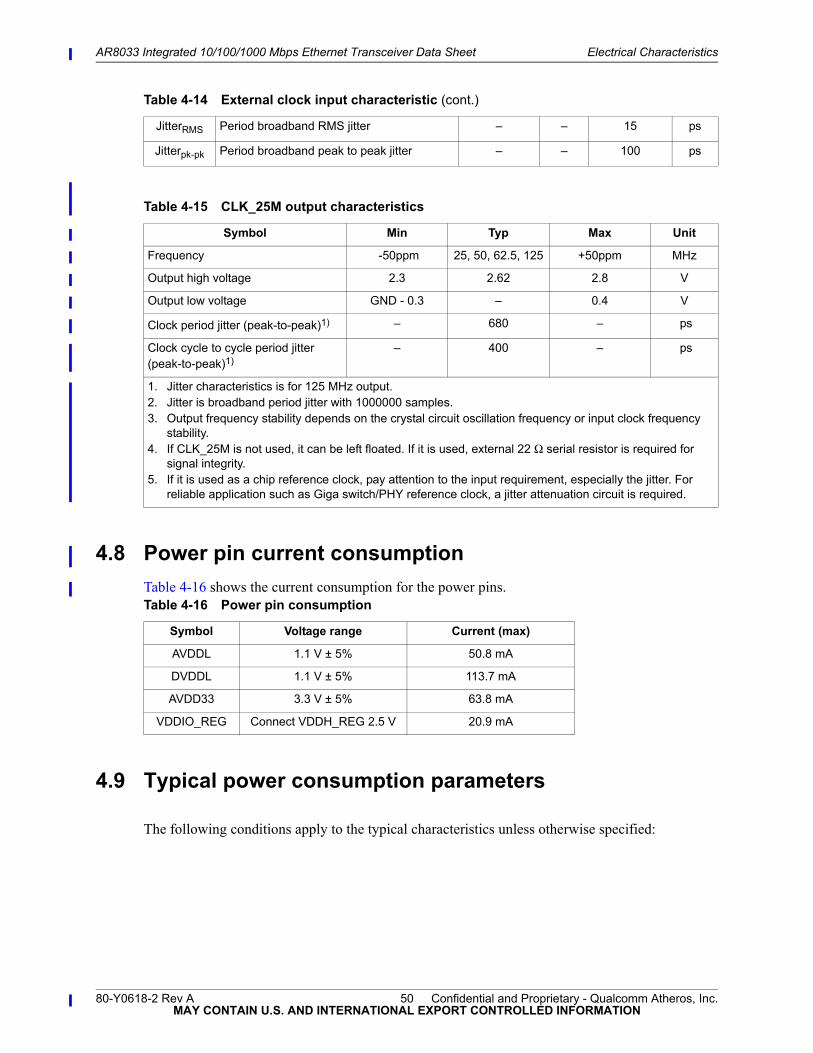
Symbol Parameter Min Typ Max Unit
T_XI_PER XI Clock Period 40.0 - 50ppm 40.0 40.0 + 50ppm ns
T_XI_HI XI Clock High 14 20.0 – ns
T_XI_LO XI Clock Low 14 20.0 – ns
T_XI_RISE XI Clock Rise Time, VIL (max) to VIH (min) – – 4 ns
T_XI_FALL XI Clock Fall time, VIL (max) TO VIH (min) – – 4 ns
V_IH_XI The XI input high level 0.8 1.2 1.5 V
V_IL_XI The XI input low level voltage -0.3 0 0.15 V
CIN Load capacitance – 1 2 pF
12
327 pF 27 pF
XTLI
XTLOAR803325 MHz
80-Y0618-2 Rev A 49 Confidential and Proprietary - Qualcomm Atheros, Inc.MAY CONTAIN U.S. AND INTERNATIONAL EXPORT CONTROLLED INFORMATION
AR8033 Integrated 10/100/1000 Mbps Ethernet Transceiver Data Sheet Electrical Characteristics
4.8 Power pin current consumption
Table 4-16 shows the current consumption for the power pins.
4.9 Typical power consumption parameters
The following conditions apply to the typical characteristics unless otherwise specified:
JitterRMS Period broadband RMS jitter – – 15 ps
Jitterpk-pk Period broadband peak to peak jitter – – 100 ps
Table 4-15 CLK_25M output characteristics
Symbol Min Typ Max Unit
Frequency -50ppm 25, 50, 62.5, 125 +50ppm MHz
Output high voltage 2.3 2.62 2.8 V
Output low voltage GND - 0.3 – 0.4 V
Clock period jitter (peak-to-peak)1) – 680 – ps
Clock cycle to cycle period jitter (peak-to-peak)1)
– 400 – ps
1. Jitter characteristics is for 125 MHz output.2. Jitter is broadband period jitter with 1000000 samples.3. Output frequency stability depends on the crystal circuit oscillation frequency or input clock frequency
stability.4. If CLK_25M is not used, it can be left floated. If it is used, external 22 Ω serial resistor is required for
signal integrity.5. If it is used as a chip reference clock, pay attention to the input requirement, especially the jitter. For
reliable application such as Giga switch/PHY reference clock, a jitter attenuation circuit is required.
P1000F 1000BASE-X full-duplex line speed 27 2.7 89.1
P1000idle 1000BASE-X idle 25 4 82.6
P100F 100BASE-FX full-duplex line speed 17 3.5 56
P100idle 100BASE-FX idle 17 4 56
RGMII + Fiber Converter mode
P1000F 1000BASE-T to 1000BASE-X full-duplex line speed
143 2.7 471.9
P1000idle 1000BASE-T to 1000BASE-X idle 134 4 442.2
P100F 100BASE-TX to 100BASE-FX full-duplex line speed
38 3.5 125.4
P100idle 100BASE-TX to 100BASE-FX idle 37 4 122.1
80-Y0618-2 Rev A 51 Confidential and Proprietary - Qualcomm Atheros, Inc.MAY CONTAIN U.S. AND INTERNATIONAL EXPORT CONTROLLED INFORMATION
AR8033 Integrated 10/100/1000 Mbps Ethernet Transceiver Data Sheet Electrical Characteristics
NOTE Power consumption test results are based on the demo board.
4.10 Power-on sequence, reset and clock
4.10.1 Power-on sequence
AR8033 only requires a single 3.3 V power supply input. The 1.1 V core and 2.5 V, 1.8/1.5 V voltages are generated by AR8033 internal regulators. So the AR8033 power-on sequence to establish the power rails stability is met internally.
4.10.2 Reset and clock timing
The AR8033 hardware reset requires the clock to take effect. Input clock including the crystal and external input clock must be stable for at least 1 ms before RESET can be de-asserted. For chip reliability, an external clock must be input after the power-on sequence.
Figure 4-5 shows the reset timing diagram.
SGMII + Copper mode
P1000F 1000BASE-T full-duplex line speed 141 2.7 465.3
P1000idle 1000BASE-T idle 133 4 438.9
P100F 100BASE-TX full-duplex line speed 39 4 128.7
P100idle 100BASE-TX idle 38 4 125.4
SGMII + Copper mode 802.3az enabled
P1000idle 1000BASE-T idle 27 4 89.1
P100idle 100BASE-TX idle 23 4 75.9
Table 4-17 Total system power (cont.)
Symbol ConditionTotal current
(mA)
LED consumption
(mA)
Total power consumption
without LED (mW)
80-Y0618-2 Rev A 52 Confidential and Proprietary - Qualcomm Atheros, Inc.MAY CONTAIN U.S. AND INTERNATIONAL EXPORT CONTROLLED INFORMATION
AR8033 Integrated 10/100/1000 Mbps Ethernet Transceiver Data Sheet Electrical Characteristics
Figure 4-5 Reset timing diagram
NOTE When using crystal, clock is generated internally after the power is stable. To get reliable power-on reset, keep asserting the reset low signal long enough to ensure that the clock is stable and clock-to-reset (1 ms) requirement is satisfied.
4.11 Digital pin design guide
3.3V
XI clock
Reset
> 0ms
>= 1ms >= 1ms
~~
Table 4-18 Digital pin designs
Pin type Pin description Reset asserted Reset de-asserted (Normal working level)
Input TXD[3:0]
TX_EN
GTX_CLK
Input, internal weak PD Input, based on RGMII I/O voltage level set
I/O RXD[3:0]
RX_DV
RX_CLK
Input, internal weak PD Output, based on RGMII I/O voltage level set
I/O LED_1000
LED_ACT
LED_10_100
Input, internal weak PU Output, 2.5 V (VDDH_REG)
Input MDC Input, internal weak PU Input, 2.5 V (3.3 V tolerant)
I/O MDIO Input, internal weak PU I/O, 2.5 V (3.3 V tolerant)
Input RSTn Input, no weak PU Input, 2.5 V (3.3 V tolerant)
Output INT
WOL_INT
Output, kept driving low Open drain output (default), based on external PU voltage level
Output CLK_25M Output, output clock Output, 2.5 V (VDDH_REG)
80-Y0618-2 Rev A 53 Confidential and Proprietary - Qualcomm Atheros, Inc.MAY CONTAIN U.S. AND INTERNATIONAL EXPORT CONTROLLED INFORMATION
AR8033 Integrated 10/100/1000 Mbps Ethernet Transceiver Data Sheet Electrical Characteristics
Output PPS Output, kept driving high 2.5 V (VDDH_REG), internal RTC clock output
Input SD Input, weak PD Input, VIH min = 0.7 V, VIL max = 0.4 V. Input must be lower than 1.4 V.
1. When MDC/MDIO/RESET acts as an input, VIH min is 1.7 V, VIL max is 0.7 V, thus the chip supports 2.5/3.3 V LVTTL/LVCMOS level signal input.
2. Power-on strapping pins are input when reset is asserted. They are output during normal operation. External pull-up to VDDIO_REG for RGMII signal, and to 2.5 V (VDDH_REG) for LED are recommended.
3. RESET and MDIO can be pulled up to 2.5 V (VDDH_REG) or 3.3 V.4. SD is a backup solution used for signal detection. Because AR8033 integrates the signal
detection function in SerDes, leaving the pin floated is recommended. When the pin is pulled high, valid signal is detected; when pulled low, no valid signal is detected.
Table 4-18 Digital pin designs (cont.)
Pin type Pin description Reset asserted Reset de-asserted (Normal working level)
80-Y0618-2 Rev A 54 Confidential and Proprietary - Qualcomm Atheros, Inc.MAY CONTAIN U.S. AND INTERNATIONAL EXPORT CONTROLLED INFORMATION
5 Registers
Three types of registers are present on AR8033:
IEEE defined 32 MII registers, referred to as “MII Registers” in this document
MII registers are accessed directly through the management frame.
Debug registers defined by Qualcomm Atheros, referred to as “Debug Registers” in this document
Write the offset address of debug register to 0x1D.
Read/write the data from/to 0x1E.
IEEE defined MDIO Manageable Device (MMD) register, referred to as “MDIO Interface (MMD3/MMD7) Registers” in this document
MMD registers are accessed by reading/writing MMD access control register (MII register 0xD) and MMD access data register (MII register 0xE).
Example: Writing 0x8000 to register 0x0 of MMD3
1. Write 0x3 to MII register 0xD to set the device address of the MMD register.
2. Write 0x0 to MII register 0xE to set the offset address of the MMD register.
3. Write 0x4003 to MII register 0xD to keep the device address.
4. Read MII register 0xE to check the data from register 0x0 of MMD3.
5. Write 0x8000 to MII register 0xE, that is register 0x0 of MMD3.
NOTE Read operation follows the process 1 to 4.
5.1 Register bit type
Table 5-1 shows the register bit types.
Table 5-1 Register bit types
Type Description
LH Register field with latching high function. If status is high, then the register is set to one and remains set until a read operation is performed through the management interface or a reset occurs.
LL Register field with latching low function. If status is low, then the register is cleared to a zero and remains cleared until a read operation is performed through the management interface or a reset occurs.
80-Y0618-2 Rev A 55 Confidential and Proprietary - Qualcomm Atheros, Inc.MAY CONTAIN U.S. AND INTERNATIONAL EXPORT CONTROLLED INFORMATION
AR8033 Integrated 10/100/1000 Mbps Ethernet Transceiver Data Sheet Registers
5.2 MII registers
Retain Value written to a register field takes effect without a software reset.
SC Self-clear. Writing a one to this register causes the desired function to execute immediately, and the register field clears to zero when the function is complete.
Update The value written to the register field does not take effect until a software reset is executed. The value can still be read after it is written.
Table 5-1 Register bit types (cont.)
Type Description
Table 5-2 Register summary
Offset Register
0x00 “Control register — copper page” on page 57
“Control register — fiber page” on page 58
0x01 “Status register — copper page” on page 60
“Status register — fiber page” on page 61
0x02 “PHY identifier 1 register” on page 63
0x03 “PHY identifier 2 register” on page 63
0x04 “Auto-negotiation advertisement register — copper page” on page 64
“Auto-negotiation advertisement register — fiber page” on page 66
0x05 “Auto-negotiation link partner ability register — copper page” on page 67
“Auto-negotiation link partner ability register — fiber page” on page 69
0x06 “Auto-negotiation expansion register — copper page” on page 70
“Auto-negotiation expansion register — fiber page” on page 70
0x07 “Auto-negotiation next page transmit register — copper page” on page 71
“Auto-negotiation next page transmit register — fiber page for 1000BASE-X, SGMII” on page 72
0x08 “Auto-negotiation link partner next page register — copper page” on page 72
“Auto-negotiation link partner next page register — fiber page for 1000BASE-X, SGMII” on page 73
0x09 “1000BASE-T control register” on page 74
0x0A “1000BASE-T status register” on page 76
0x0B Reserved
0x0C Reserved
0x0D “MMD access control register” on page 77
0x0E “MMD access data register” on page 77
0x0F “Extended status register” on page 77
0x10 “PHY specific function control register” on page 78
0x11 “PHY specific status register — copper page” on page 79
“PHY specific status register — fiber page” on page 81
80-Y0618-2 Rev A 56 Confidential and Proprietary - Qualcomm Atheros, Inc.MAY CONTAIN U.S. AND INTERNATIONAL EXPORT CONTROLLED INFORMATION
AR8033 Integrated 10/100/1000 Mbps Ethernet Transceiver Data Sheet Registers
5.2.1 Control register — copper page
Offset: 0x00
0x12 “Interrupt enable register” on page 82
0x13 “Interrupt status register” on page 83
0x14 “Smart speed register” on page 85
0x15 Reserved
0x16 “Cable diagnostic test control register” on page 86
0x17 Reserved
0x18 “LED control register” on page 86
0x19 “Manual LED override register” on page 87
0x1A Reserved
0x1B “Copper/fiber status register” on page 88
0x1C “Cable diagnostic test status register” on page 90
0x1D “Debug port — address offset register” on page 90
0x1E “Debug port — dataport register” on page 90
0x1F “Chip configure register” on page 91
For most MII Register offset addresses, each address has two pages. One for copper port, and the other for fiber port.
When 0x1F[15] = 0, the MII register shows fiber page.
When 0x1F[15] = 1, the MII register shows copper page.For typical application, poll the PHY specific status register to get link/speed/duplex information and then configure MAC before sending and receiving packets.
Table 5-2 Register summary (cont.)
Offset Register
Bit Name Type Description
15 RESET Mode R/W PHY Software Reset. Writing 1 to this bit causes immediate PHY reset. When the operation is done, this bit is cleared automatically.
1 = PHY reset
0 = Normal operation
HW Rst. 0
SW Rst. SC
14 LOOPBACK Mode R/W When loopback is activated, the transmitter data on TXD is looped back to RXD internally.
80-Y0618-2 Rev A 57 Confidential and Proprietary - Qualcomm Atheros, Inc.MAY CONTAIN U.S. AND INTERNATIONAL EXPORT CONTROLLED INFORMATION
AR8033 Integrated 10/100/1000 Mbps Ethernet Transceiver Data Sheet Registers
5.2.2 Control register — fiber page
Offset: 0x00
12 AUTO-NEGOTIATION
Mode R/W 1 = Enable auto-negotiation process
0 = Disable auto-negotiation processHW Rst. 1
SW Rst. Retain
11 POWER DOWN Mode R/W When the port is switched from power down to normal operation, software reset and restart Auto-negotiation are performed even when bit[15] RESET and bit[9] RESTART AUTO-NEGOTIATION are not set.
1 = Power-down
0 = Normal operation
HW Rst. 0
SW Rst. 0
10 ISOLATE Mode R/W The RGMII output pins are tri-stated when this bit is 1. The RGMII inputs are ignored.
1 = Isolate
0 = Normal operation
HW Rst. 0
SW Rst. 0
9 RESTART AUTO-NEGOTIATION
Mode R/W, SC
Auto-negotiation automatically restarts after hardware or software reset regardless of whether this bit is set or not.
1 = Restart auto-negotiation process
0 = Normal operation
HW Rst. 0
SW Rst. 0
8 DUPLEX MODE Mode R/W 1 = Full-duplex
0 = Half-duplexHW Rst. 1
SW Rst. Retain
7 COLLISION TEST Mode R/W Setting this bit to 1 asserts the COL pin whenever the TX_EN pin is asserted.
1 = Enable COL signal test
0 = Disable COL signal test
HW Rst. 0
SW Rst. 0
6 SPEED SELECTION (MSB)
Mode R/W See bit[13] SPEED SELECTION (LSB)
HW Rst. 0
SW Rst. 0
5:0 RESERVED Mode R/O Always 0
HW Rst. 0
SW Rst. 0
Bit Name Type Description
Bit Name Type Description
15 RESET Mode R/W PHY software reset. Writing 1 to this bit causes immediate PHY reset. When the operation is done, this bit is cleared automatically.
1 = PHY reset
0 = Normal operation
HW Rst. 0
SW Rst. SC
80-Y0618-2 Rev A 58 Confidential and Proprietary - Qualcomm Atheros, Inc.MAY CONTAIN U.S. AND INTERNATIONAL EXPORT CONTROLLED INFORMATION
AR8033 Integrated 10/100/1000 Mbps Ethernet Transceiver Data Sheet Registers
14 LOOPBACK Mode R/W 100BASE-FX, 1000BASE-X, SGMII loopback. When loopback is activated, 10-bit TXD to SerDes is looped back to 10-bit RXD.
The force speed is valid only when bit[12] AUTO-NEGOTIATION is 0.
HW Rst. 0
SW Rst. Retain
12 AUTO-NEGOTIATION
Mode R/W For 1000BASE-X, SGMII:
1 = Enable auto-negotiation process
0 = Disable auto-negotiation process
No auto-negotiation in 100BASE-FX
HW Rst. 1
SW Rst. 1
11 POWER DOWN Mode R/W For 100BASE-FX, 1000BASE-X, SGMII mode:
When the port is switched from power-down to normal operation, software reset and restart Auto-Negotiation are performed even when bit[15] RESET and bit[9] RESTART AUTO-NEGOTIATION are not set.
1 = Power-down, shut off SerDes
0 = Normal operation
HW Rst. 0
SW Rst. Retain
10 ISOLATE Mode R/W Not implement
HW Rst. 0
SW Rst. 0
9 RESTART AUTO-NEGOTIATION
Mode R/W, SC
For 1000BASE-X, SGMII:
Auto-negotiation automatically restarts after hardware or software reset regardless of whether or not this bit is set.
1 = Restart auto-negotiation process
0 = Normal operation
HW Rst. 0
SW Rst. SC
8 DUPLEX MODE Mode R/W, Takes effect in 1000BASE-X auto-negotiation disable (bit[12] AUTO-NEGOTIAION = 0) mode, or 100BASE-FX mode:
1 = Full-duplex
0 = Half-duplex
HW Rst. 1
SW Rst. Retain
7 COLLISION TEST Mode R/W N/A
HW Rst. 0
SW Rst. 0
6 SPEED SELECTION (MSB)
Mode R/W See bit[13] SPEED SELECTION (LSB)
HW Rst. 1
SW Rst. Retain
Bit Name Type Description
80-Y0618-2 Rev A 59 Confidential and Proprietary - Qualcomm Atheros, Inc.MAY CONTAIN U.S. AND INTERNATIONAL EXPORT CONTROLLED INFORMATION
AR8033 Integrated 10/100/1000 Mbps Ethernet Transceiver Data Sheet Registers
5.2.3 Status register — copper page
Offset: 0x01
5:0 RESERVED Mode R/W Always 0
HW Rst. 0
SW Rst. 0
Bit Name Type Description
Bit Name Type Description
15 100BASE-T4 Mode RO 100BASE-T4
Always 0
This protocol is not available.
1 = PHY supports 100BASE-T4.
0 = PHY does not support 100BASE-T4.
HW Rst. 0
SW Rst. 0
14 100BASE-TX FULL-DUPLEX
Mode RO Always 1
1 = PHY supports 100BASE-TX full-duplex.
0 = PHY does not support 100BASE-TX full-duplex.HW Rst. 1
SW Rst. 1
13 100BASE-TX HALF-DUPLEX
Mode RO Always 1
1 = PHY supports 100BASE-TX half-duplex.
0 = PHY does not support 100BASE-TX half-duplex.HW Rst. 1
SW Rst. 1
12 10BASE-T FULL-DUPLEX
Mode RO Always 1
1 = PHY supports 10BASE-T full-duplex.
0 = PHY does not support 10BASE-T full-duplex.HW Rst. 1
SW Rst. 1
11 10BASE-T HALF-DUPLEX
Mode RO Always 1
1 = PHY supports 10BASE-T half-duplex.
0 = PHY does not support 10BASE-T half-duplex.HW Rst. 1
SW Rst. 1
10 100BASE-T2 FULL-DUPLEX
Mode RO Always 0
1 = PHY supports 100BASE-T2.
0 = PHY does not support 100BASE-T2.HW Rst. 0
SW Rst. 0
9 100BASE-T2 HALF-DUPLEX
Mode RO Always 0
1 = PHY supports 100BASE-T2.
0 = PHY does not support 100BASE-T2.HW Rst. 0
SW Rst. 0
8 EXTENDED STATUS
Mode RO Always 1
Extended status information in Extended status register
HW Rst. 1
SW Rst. 1
7 RESERVED Mode RO Always 0
HW Rst. 0
SW Rst. 0
80-Y0618-2 Rev A 60 Confidential and Proprietary - Qualcomm Atheros, Inc.MAY CONTAIN U.S. AND INTERNATIONAL EXPORT CONTROLLED INFORMATION
AR8033 Integrated 10/100/1000 Mbps Ethernet Transceiver Data Sheet Registers
5.2.4 Status register — fiber page
Offset: 0x01
6 MF PREAMBLE SUPPRESSION
Mode RO Always 1
1 = PHY accepts management frames with preamble suppressed.
0 = PHY does not accept management frames with preamble suppressed.
HW Rst. 1
SW Rst. 1
5 AUTO-NEGOTIATION COMPLETE
Mode RO 1 = Auto-negotiation process completed
0 = Auto-negotiation process not completedHW Rst. 0
0 = PHY does not support auto-negotiation.HW Rst. 1
SW Rst. 1
2 LINK STATUS Mode RO, LL This bit indicates whether the link was lost since the last read. For the current link status, see bit[10] LINK (REAL-TIME) of register PHY specific status register — copper page.
0 = PHY does not support auto-negotiation.HW Rst. 1
SW Rst. 1
Bit Name Type Description
80-Y0618-2 Rev A 62 Confidential and Proprietary - Qualcomm Atheros, Inc.MAY CONTAIN U.S. AND INTERNATIONAL EXPORT CONTROLLED INFORMATION
AR8033 Integrated 10/100/1000 Mbps Ethernet Transceiver Data Sheet Registers
5.2.5 PHY identifier 1 register
Offset: 0x02
5.2.6 PHY identifier 2 register
Offset: 0x03
2 LINK STATUS Mode RO, LL This bit indicates whether the link is lost since the last read. For the current link status, see bit[10] LINK (REAL-TIME) of register PHY specific status register — fiber page.
15 NEXT PAGE Mode R/W The value of this bit is updated immediately after writing this register. The value written to this bit takes effect only when any one of the following occurs:
Software reset is asserted (bit[15] RESET of Control register — copper page)
Restart Auto-Negotiation is asserted (bit[9] RESTART AUTO-NEGOTIATION of Control register — copper page)
Power-down (bit[11] POWER DOWN of Control register — copper page) transitions from power down to normal operation
Link goes down
If 1000BASE-T is advertised, the required next pages are automatically transmitted. Bit[15] NEXT PAGE of Auto-negotiation advertisement register — copper page must be set to 0 if no additional next pages are required.
1 = Advertise
0 = Not advertised
HW Rst. 0
SW Rst. Update
14 ACK Mode RO Always 0
HW Rst. 0
SW Rst. 0
13 REMOTE FAULT Mode R/W 1 = Set Remote Fault bit
0 = Do not set Remote Fault bitHW Rst. 0
SW Rst. Update
12 XNP_ABLE Mode R/W Extended next page enable control bit:
1 = Local device supports transmission of extended next pages.
0 = Local device does not support transmission of extended next pages.
HW Rst. Always 1
SW Rst. Retain
11 ASYMMETRIC PAUSE
Mode R/W The value of this bit is updated immediately after writing this register. The value written to this bit takes effect only when any one of the following occurs:
Software reset is asserted (bit[15] RESET of Control register — copper page)
Restart Auto-Negotiation is asserted (bit[9] RESTART AUTO-NEGOTIATION of Control register — copper page)
Power-down (bit[11] POWER DOWN of Control register — copper page) transitions from power down to normal operation
Link goes down
1 = Asymmetric pause
0 = No asymmetric pause
HW Rst. 1
SW Rst. Update
80-Y0618-2 Rev A 64 Confidential and Proprietary - Qualcomm Atheros, Inc.MAY CONTAIN U.S. AND INTERNATIONAL EXPORT CONTROLLED INFORMATION
AR8033 Integrated 10/100/1000 Mbps Ethernet Transceiver Data Sheet Registers
10 PAUSE Mode R/W The value of this bit is updated immediately after writing this register. The value written to this bit takes effect only when any one of the following occurs:
Software reset is asserted (bit[15] RESET of Control register — copper page)
Restart Auto-Negotiation is asserted (bit[9] RESTART AUTO-NEGOTIATION of Control register — copper page)
Power-down (bit[11] POWER DOWN of Control register — copper page) transitions from power down to normal operation
Link goes down
1 = MAC PAUSE implemented
0 = MAC PAUSE not implemented
HW Rst. 1
SW Rst. Update
9 100BASE-T4 Mode RO Always 0
1 = PHY supports 100BASE-T4.
0 = PHY does not support 100BASE-T4.HW Rst. 0
SW Rst. 0
8 100BASE-TX FULL DUPLEX
Mode R/W The value of this bit is updated immediately after writing this register. The value written to this bit takes effect only when any one of the following occurs:
Software reset is asserted (bit[15] RESET of Control register — copper page)
Restart Auto-Negotiation is asserted (bit[9] RESTART AUTO-NEGOTIATION of Control register — copper page)
Power-down (bit[11] POWER DOWN of Control register — copper page) transitions from power down to normal operation
Link goes down
1 = Advertise
0 = Not advertised
HW Rst. 1
SW Rst. Update
7 100BASE-TX HALF DUPLEX
Mode R/W The value of this bit is updated immediately after writing this register. The value written to this bit takes effect only when any one of the following occurs:
Software reset is asserted (bit[15] RESET of Control register — copper page)
Restart Auto-Negotiation is asserted (bit[9] RESTART AUTO-NEGOTIATION of Control register — copper page)
Power-down (bit[11] POWER DOWN of Control register — copper page) transitions from power down to normal operation
Link goes down
1 = Advertise
0 = Not advertised
HW Rst. 1
SW Rst. Update
Bit Name Type Description
80-Y0618-2 Rev A 65 Confidential and Proprietary - Qualcomm Atheros, Inc.MAY CONTAIN U.S. AND INTERNATIONAL EXPORT CONTROLLED INFORMATION
AR8033 Integrated 10/100/1000 Mbps Ethernet Transceiver Data Sheet Registers
Mode R/W The value of this bit is updated immediately after writing this register. The value written to this bit takes effect only when any one of the following occurs:
Software reset is asserted (bit[15] RESET of Control register — copper page)
Restart Auto-Negotiation is asserted (bit[9] RESTART AUTO-NEGOTIATION of Control register — copper page)
Power-down (bit[11] POWER DOWN of Control register — copper page) transitions from power down to normal operation
Link goes down
1 = Advertise
0 = Not advertised
HW Rst. 1
SW Rst. Update
5 10BASE-T HALF DUPLEX
Mode R/W The value of this bit is updated immediately after writing this register. The value written to this bit takes effect only when any one of the following occurs:
Software reset is asserted (bit[15] RESET of Control register — copper page)
Restart Auto-Negotiation is asserted (bit[9] RESTART AUTO-NEGOTIATION of Control register — copper page)
Power-down (bit[11] POWER DOWN of Control register — copper page) transitions from power down to normal operation
Link goes down
1 = Advertise
0 = Not advertised
HW Rst. 1
SW Rst. Update
4:0 SELECTOR FIELD Mode RO Selector field mode
Always 1
1 = IEEE 802.3HW Rst. 1
SW Rst. 1
Bit Name Type Description
Bit Name Type Description
15 NEXT PAGE Mode R/W This bit indicates if additional next pages are required.
1 = Advertise
0 = Not advertisedHW Rst. 0
SW Rst. Update
14 ACK Mode RO Always 0
HW Rst. 0
SW Rst. 0
80-Y0618-2 Rev A 66 Confidential and Proprietary - Qualcomm Atheros, Inc.MAY CONTAIN U.S. AND INTERNATIONAL EXPORT CONTROLLED INFORMATION
AR8033 Integrated 10/100/1000 Mbps Ethernet Transceiver Data Sheet Registers
5.2.9 Auto-negotiation link partner ability register — copper page
Offset: 0x05
13:12 REMOTE FAULT Mode R/W 00 = LINK_OK
01 = OFFLINE
10 = LINK_FAILURE
11 = AUTO_ERROR
HW Rst. 00
SW Rst. Update
11:9 RESERVED Mode R/W –
HW Rst. 0
SW Rst. 0
8 ASYMMETRIC PAUSE
Mode R/W 1 = Asymmetric pause
0 = No asymmetric pauseHW Rst. 1
SW Rst. Update
7 PAUSE Mode R/W 1 = MAC PAUSE implemented
0 = MAC PAUSE not implementedHW Rst. 1
SW Rst. Update
6 1000BASE-X HALF DUPLEX
Mode R/W 1000BASE-X half-duplex ability
HW Rst. 0
SW Rst. Retain
5 1000BASE-X FULL DUPLEX
Mode R/W 1000BASE-X full-duplex ability
HW Rst. 1
SW Rst. Retain
4:0 RESERVED Mode RO Always 0
HW Rst. 0
SW Rst. 0
Bit Name Type Description
Bit Name Type Description
15 NEXT PAGE Mode RO Received code word bit[15]
1 = Link partner supports Next Page
0 = Link partner does not support Next PageHW Rst. 0
SW Rst. 0
14 ACK Mode RO Acknowledge
Received code word bit[14]
1 = Link partner successfully received link code word
0 = Link partner failed to receive link code word
HW Rst. 0
SW Rst. 0
13 REMOTE FAULT Mode RO Remote fault
Received code word bit[13]
1 = Link partner detects remote fault
0 = Link partner does not detect remote fault
HW Rst. 0
SW Rst. 0
80-Y0618-2 Rev A 67 Confidential and Proprietary - Qualcomm Atheros, Inc.MAY CONTAIN U.S. AND INTERNATIONAL EXPORT CONTROLLED INFORMATION
AR8033 Integrated 10/100/1000 Mbps Ethernet Transceiver Data Sheet Registers
12 RESERVED Mode RO Technology ability field
Received code word bit[12]HW Rst. 0
SW Rst. 0
11 ASYMMETRIC PAUSE
Mode RO Technology ability field
Received code word bit[11]
1 = Link partner requests asymmetric pause
0 = Link partner does not request asymmetric pause
HW Rst. 0
SW Rst. 0
10 PAUSE Mode RO Technology ability field
Received code word bit[10]
1 = Link partner supports pause operation
0 = Link partner does not support pause operation
HW Rst. 0
SW Rst. 0
9 100BASE-T4 Mode RO Technology ability field
Received code word bit[9]
1 = Link partner supports 100BASE-T4
0 = Link partner does not support 100BASE-T4
HW Rst. 0
SW Rst. 0
8 100BASE-TX FULL DUPLEX
Mode RO Technology ability field
Received code word bit[8]
1 = Link partner supports 100BASE-TX full-duplex
0 = Link partner does not support 100BASE-TX full-duplex
HW Rst. 0
SW Rst. 0
7 100BASE-TX HALF DUPLEX
Mode RO Technology ability field
Received code word bit[7]
1 = Link partner supports 100BASE-TX half-duplex
0 = Link partner does not support 100BASE-TX half-duplex
HW Rst. 0
SW Rst. 0
6 10BASE-T FULL DUPLEX
Mode RO Technology ability field
Received code word bit[6]
1 = Link partner support 10BASE-T full-duplex
0 = Link partner does not support 10BASE-T full-duplex
HW Rst. 0
SW Rst. 0
5 10BASE-T HALF DUPLEX
Mode RO Technology ability field
Received code word bit[5]
1 = Link partner supports 10BASE-T half-duplex
0 = Link partner does not support 10BASE-T half-duplex
HW Rst. 0
SW Rst. 0
4:0 SELECTOR FIELD Mode RO Selector field
Received code word bit[4:0]HW Rst. 0
SW Rst. 0
Bit Name Type Description
80-Y0618-2 Rev A 68 Confidential and Proprietary - Qualcomm Atheros, Inc.MAY CONTAIN U.S. AND INTERNATIONAL EXPORT CONTROLLED INFORMATION
AR8033 Integrated 10/100/1000 Mbps Ethernet Transceiver Data Sheet Registers
5.2.10 Auto-negotiation link partner ability register — fiber page
Offset: 0x05
Bit Name Type Description
15 NEXT PAGE Mode RO Received code word bit[15]
1 = Link partner supports Next Page
0 = Link partner does not support Next PageHW Rst. 0
SW Rst. 0
14 ACK Mode RO Acknowledge
Received code word bit[14]
1 = Link partner received link code word
0 = Link partner does not have Next Page ability
HW Rst. 0
SW Rst. 0
13:12 REMOTE FAULT Mode RO Remote fault
Received code word bit[13:12]HW Rst. 0
SW Rst. 0
11:9 RESERVED Mode RO –
HW Rst. 0
SW Rst. 0
8 ASYMMETRIC PAUSE
Mode RO Technology ability field
Received code word bit[8]
1 = Link partner requests asymmetric pause
0 = Link partner does not request asymmetric pause
HW Rst. 0
SW Rst. 0
7 PAUSE Mode RO Technology ability field
Received code word bit[7]
1 = Link partner supports pause operation
0 = Link partner does not support pause operation
HW Rst. 0
SW Rst. 0
6 1000 BASE-X HALF DUPLEX
Mode RO Technology ability field
Received code word bit[6]
1 = Link partner supports 1000BASE-X half-duplex
0 = Link partner does not support 1000BASE-X half-duplex
HW Rst. 0
SW Rst. 0
5 1000 BASE-X FULL DUPLEX
Mode RO Technology ability field
Received code word bit[6]
1 = Link partner supports 1000BASE-X full-duplex
0 = Link partner does not support 1000BASE-X full-duplex
HW Rst. 0
SW Rst. 0
4:0 RESERVED Mode RO –
HW Rst. 0
SW Rst. 0
80-Y0618-2 Rev A 69 Confidential and Proprietary - Qualcomm Atheros, Inc.MAY CONTAIN U.S. AND INTERNATIONAL EXPORT CONTROLLED INFORMATION
AR8033 Integrated 10/100/1000 Mbps Ethernet Transceiver Data Sheet Registers
0 = Link partner does not support Next PageHW Rst. 0
SW Rst. 0
2 LOCAL NEXT PAGE ABLE
Mode RO 1 = Local device supports Next Page
0 = Local device does not support Next PageHW Rst. 1
SW Rst. 1
1 PAGE RECEIVED Mode RO, LH
1 = A new page is received
0 = No new page is received
HW Rst. 0
SW Rst. 0
0 LINK PARTNER AUTO-NEGOTIATION ABLE
Mode RO 1 = Link partner supports auto-negotiation
0 = Link partner does not support auto-negotiationHW Rst. 0
SW Rst. 0
Bit Name Type Description
15:4 RESERVED Mode RO Always 0
HW Rst. 0
SW Rst. 0
3 LINK PARTNER NEXT PAGE ABLE
Mode RO For 1000BASE-X, SGMII:
1 = Link partner supports Next Page
0 = Link partner does not support Next PageHW Rst. 0
SW Rst. 0
2 LOCAL NEXT PAGE ABLE
Mode RO For 1000BASE-X, SGMII:
1 = Local device supports Next Page
0 = Local device does not support Next PageHW Rst. 1
SW Rst. 1
80-Y0618-2 Rev A 70 Confidential and Proprietary - Qualcomm Atheros, Inc.MAY CONTAIN U.S. AND INTERNATIONAL EXPORT CONTROLLED INFORMATION
AR8033 Integrated 10/100/1000 Mbps Ethernet Transceiver Data Sheet Registers
5.2.13 Auto-negotiation next page transmit register — copper page
Offset: 0x07
1 PAGE RECEIVED Mode RO For 1000BASE-X, SGMII:
1 = A new page is received
0 = No new page is receivedHW Rst. 0
SW Rst. 0
0 LINK PARTNER AUTO NEGOTIATION ABLE
Mode RO, LH For 1000BASE-X, SGMII:
1 = Link partner supports auto-negotiation
0 = Link partner does not support auto-negotiationHW Rst. 0
SW Rst. 0
Bit Name Type Description
Bit Name Type Description
15 NEXT PAGE Mode R/W Transmit code word bit[15]
HW Rst. 0
SW Rst. 0
14 RESERVED Mode R/W Transmit code word bit[14]
HW Rst. 0
SW Rst. 0
13 MESSAGE PAGE MODE Mode R/W Transmit code word bit[13]
HW Rst. 1
SW Rst. 1
12 ACK2 Mode R/W Transmit code word bit[12]
HW Rst. 1
SW Rst. 1
11 TOGGLE Mode RO Transmit code word bit[11]
HW Rst. 0
SW Rst. 0
10:0 MESSAGE/UNFORMATTED FIELD
Mode R/W Transmit code word bits[10:0]
HW Rst. 1
SW Rst. 1
80-Y0618-2 Rev A 71 Confidential and Proprietary - Qualcomm Atheros, Inc.MAY CONTAIN U.S. AND INTERNATIONAL EXPORT CONTROLLED INFORMATION
AR8033 Integrated 10/100/1000 Mbps Ethernet Transceiver Data Sheet Registers
5.2.14 Auto-negotiation next page transmit register — fiber page for 1000BASE-X, SGMII
Offset: 0x07
5.2.15 Auto-negotiation link partner next page register — copper page
Offset: 0x08
Bit Name Type Description
15 NEXT PAGE Mode R/W Transmit code word bit[15]
HW Rst. 0
SW Rst. 0
14 RESERVED Mode R/W Transmit code word bit[14]
HW Rst. 0
SW Rst. 0
13 MESSAGE PAGE MODE Mode R/W Transmit code word bit[13]
HW Rst. 1
SW Rst. 1
12 ACK2 Mode R/W Transmit code word bit[12]
HW Rst. 0
SW Rst. 0
11 TOGGLE Mode RO Transmit code word bit[11]
HW Rst. 0
SW Rst. 0
10:0 MESSAGE/UNFORMATTED FIELD
Mode R/W Transmit code word bits[10:0]
HW Rst. 1
SW Rst. 1
Bit Name Type Description
15 NEXT PAGE Mode RO Received code word bit[15]
HW Rst. 0
SW Rst. 0
14 RESERVED Mode RO Received code word bit[14]
HW Rst. 0
SW Rst. 0
80-Y0618-2 Rev A 72 Confidential and Proprietary - Qualcomm Atheros, Inc.MAY CONTAIN U.S. AND INTERNATIONAL EXPORT CONTROLLED INFORMATION
AR8033 Integrated 10/100/1000 Mbps Ethernet Transceiver Data Sheet Registers
5.2.16 Auto-negotiation link partner next page register — fiber page for 1000BASE-X, SGMII
Offset: 0x08
13 MESSAGE PAGE MODE Mode RO Received code word bit[13]
HW Rst. 0
SW Rst. 0
12 ACK2 Mode RO Received code word bit[12]
HW Rst. 1
SW Rst. 1
11 TOGGLE Mode RO Received code word bit[11]
HW Rst. 1
SW Rst. 1
10:0 MESSAGE/UNFORMATTED FIELD
Mode RO Received code word bits[10:0]
HW Rst. 0
SW Rst. 0
Bit Name Type Description
Bit Name Type Description
15 NEXT PAGE Mode RO Received code word bit[15]
HW Rst. 0
SW Rst. 0
14 RESERVED Mode RO Received code word bit[14]
HW Rst. 0
SW Rst. 0
13 MESSAGE PAGE MODE Mode RO Received code word bit[13]
HW Rst. 0
SW Rst. 0
12 ACK2 Mode RO Received code word bit[12]
HW Rst. 0
SW Rst. 0
11 TOGGLE Mode RO Received code word bit[11]
HW Rst. 0
SW Rst. 0
10:0 MESSAGE/UNFORMATTED FIELD
Mode RO Received code word bits[10:0]
HW Rst. 0
SW Rst. 0
80-Y0618-2 Rev A 73 Confidential and Proprietary - Qualcomm Atheros, Inc.MAY CONTAIN U.S. AND INTERNATIONAL EXPORT CONTROLLED INFORMATION
AR8033 Integrated 10/100/1000 Mbps Ethernet Transceiver Data Sheet Registers
5.2.17 1000BASE-T control register
Offset: 0x09
Bit Name Type Description
15:13 TEST MODE Mode R/W After exiting the test mode, hardware reset or software reset (bit[15] RESET of Control register — copper page) must be issued to ensure normal operation.
000 = Normal Mode
001 = Test mode 1 – Transmit waveform test
010 = Test mode 2 – Transmit jitter test (master mode)
011 = Test mode 3 – Transmit jitter test (slave mode)
100 = Test mode 4 – Transmit distortion test
101, 110, 111 = Reserved
HW Rst. 0
SW Rst. Retain
12 MASTER/SLAVE MANUAL CONFIGURATION ENABLE
Mode R/W The value of this bit is updated immediately after writing this register. The value written to this bit takes effect only when any one of the following occurs:
Software reset is asserted (bit[15] RESET of Control register — copper page)
Restart Auto-Negotiation is asserted (bit[9] RESTART_AUTO_NEGOTIATION of Control register — copper page)
Power-down (bit[11] POWER_DOWN of Control register — copper page) transitions from power down to normal operation
Link goes down
1 = Manual master/slave configuration
0 = Automatic master/slave configuration
HW Rst. 0
SW Rst. Update
11 MASTER/SLAVE CONFIGURATION
Mode R/W The value of this bit is updated immediately after writing this register. The value written to this bit takes effect only when any one of the following occurs:
Software reset is asserted (bit[15] RESET of Control register — copper page)
Restart Auto-Negotiation is asserted (bit[9] RESTART_AUTO_NEGOTIATION of Control register — copper page)
Power-down (bit[11] POWER_DOWN of Control register — copper page) transitions from power down to normal operation
Link goes down
Bit[11] MASTER/SLAVE CONFIGURATION is ignored if bit[12] MASTER/SLAVE MANUAL CONFIGURATION ENABLE = 0.
1 = Manual configure as master
0 = Manual configure as slave
HW Rst. 0
SW Rst. Update
80-Y0618-2 Rev A 74 Confidential and Proprietary - Qualcomm Atheros, Inc.MAY CONTAIN U.S. AND INTERNATIONAL EXPORT CONTROLLED INFORMATION
AR8033 Integrated 10/100/1000 Mbps Ethernet Transceiver Data Sheet Registers
10 PORT TYPE Mode R/W The value of this bit is updated immediately after writing this register. The value written to this bit takes effect only when any one of the following occurs:
Software reset is asserted (bit[15] RESET of Control register — copper page)
Restart Auto-Negotiation is asserted (bit[9] RESTART_AUTO_NEGOTIATION of Control register — copper page)
Power-down (bit[11] POWER_DOWN of Control register — copper page) transitions from power down to normal operation
Link goes down
Bit[10] PORT TYPE is ignored if bit[12] MASTER/SLAVE MANUAL CONFIGURATION ENABLE = 1.
1 = Prefer multi-port device (master)
0 = Prefer single-port device (slave)
HW Rst. 0
SW Rst. Update
9 1000BASE-T FULL DUPLEX
Mode R/W The value of this bit is updated immediately after writing this register. The value written to this bit takes effect only when any one of the following occurs:
Software reset is asserted (bit[15] RESET of Control register — copper page)
Restart Auto-Negotiation is asserted (bit[9] RESTART_AUTO_NEGOTIATION of Control register — copper page)
Power-down (bit[11] POWER_DOWN of Control register — copper page) transitions from power down to normal operation
Link goes down
1 = Advertise
0 = Not advertised
HW Rst. 1
SW Rst. Update
8 1000BASE-T HALF-DUPLEX
Mode R/W The value of this bit is updated immediately after writing this register. The value written to this bit takes effect only when any one of the following occurs:
Software reset is asserted (bit[15] RESET of Control register — copper page)
Restart Auto-Negotiation is asserted (bit[9] RESTART_AUTO_NEGOTIATION of Control register — copper page)
Power-down (bit[11] POWER_DOWN of Control register — copper page) transitions from power down to normal operation
Link goes down
1 = Advertise
0 = Not advertised
Note: The 1000BASE-T/half-duplex is not advertised by default.
HW Rst. 0
SW Rst. Update
7:0 RESERVED Mode R/W –
HW Rst. 0
SW Rst. 0
Bit Name Type Description
80-Y0618-2 Rev A 75 Confidential and Proprietary - Qualcomm Atheros, Inc.MAY CONTAIN U.S. AND INTERNATIONAL EXPORT CONTROLLED INFORMATION
AR8033 Integrated 10/100/1000 Mbps Ethernet Transceiver Data Sheet Registers
5.2.18 1000BASE-T status register
Offset: 0x0A
Bit Name Type Description
15 MASTER/SLAVE CONFIGURATION FAULT
Mode RO, LH This bit is cleared on a read operation.
1 = Master/Slave configuration fault detected
0 = No fault detectedHW Rst. 0
SW Rst. 0
14 MASTER/SLAVE CONFIGURATION RESOLUTION
Mode RO This bit is valid only when bit[1] PAGE RECEIVED of Auto-negotiation expansion register — copper page = 1.
1 = Local PHY configuration resolved to master
0 = Local PHY configuration resolved to slave
HW Rst. 0
SW Rst. 0
13 LOCAL RECEIVER STATUS
Mode RO 1 = Local receiver OK
0 = Local receiver not OKHW Rst. 0
SW Rst. 0
12 REMOTE RECEIVER STATUS
Mode RO 1 = Remote receiver OK
0 = Remote receiver not OKHW Rst. 0
SW Rst. 0
11 LINK PARTNER 1000 BASE-T FULL DUPLEX CAPABILITY
Mode RO This bit is valid only when bit[1] PAGE RECEIVED of Auto-negotiation expansion register — copper page = 1.
1 = Link partner supports 1000BASE-T full-duplex
0 = Link partner does not support 1000BASE-T full-duplex
HW Rst. 0
SW Rst. 0
10 LINK PARTNER 1000 BASE-T HALF DUPLEX CAPABILITY
Mode R/W This bit is valid only when bit[1] PAGE RECEIVED of Auto-negotiation expansion register — copper page = 1.
1 = Link partner supports 1000 BASE-T half-duplex
0 = Link partner does not support 1000 BASE-T half-duplex
HW Rst. 0
SW Rst. 0
9:8 RESERVED Mode RO Always 0
HW Rst. 0
SW Rst. 0
7:0 IDLE ERROR COUNT
Mode RO, SC MSB of idle error counter
Report the idle error count since the last time this register was read. The counter counts up to 11111111 and does roll over.
HW Rst. 0
SW Rst. 0
80-Y0618-2 Rev A 76 Confidential and Proprietary - Qualcomm Atheros, Inc.MAY CONTAIN U.S. AND INTERNATIONAL EXPORT CONTROLLED INFORMATION
AR8033 Integrated 10/100/1000 Mbps Ethernet Transceiver Data Sheet Registers
5.2.19 MMD access control register
Offset: 0x0D
5.2.20 MMD access data register
Offset: 0x0E
5.2.21 Extended status register
Offset: 0x0F
Bit Name Type Description
15:14 FUNCTION Mode R/W 00 = Address
01 = Data, no post increment
10 = Data, post increment on read and write operations
11 = Data, post increment on write operation only
HW Rst. 0
SW Rst. 0
13:5 RESERVED Mode RO –
HW Rst. 0
SW Rst. 0
4:0 DEVAD Mode R/W Device address
HW Rst. 0
SW Rst. Update
Bit Name Type Description
15:14 ADDRESS DATA
Mode R/W If bits[15:14] FUNCTION = 00 in MMD access control register, MMD DEVAD is address register.
Otherwise, MMD DEVAD is data register indicated by the contents of its address register.
See “MII registers” on page 56 for detailed information of accessing MMD registers.
HW Rst. 0
SW Rst. Retain
13:0 RESERVED – –
Bit Name Type Description
15 1000BASE-X FULL DUPLEX
Mode RO Always 1
1 = PHY supports 1000BASE-X full-duple.
0 = PHY does not support 1000BASE-X full-duple.HW Rst. 1
SW Rst. 1
14 1000BASE-X HALF DUPLEX
Mode RO Always 0
1 = PHY supports 1000BASE-X half-duplex.
0 = PHY does not support 1000BASE-X half-duplex.HW Rst. 0
SW Rst. 0
80-Y0618-2 Rev A 77 Confidential and Proprietary - Qualcomm Atheros, Inc.MAY CONTAIN U.S. AND INTERNATIONAL EXPORT CONTROLLED INFORMATION
AR8033 Integrated 10/100/1000 Mbps Ethernet Transceiver Data Sheet Registers
5.2.22 PHY specific function control register
Offset: 0x10
13 1000BASE-T FULL-DUPLEX
Mode RO Always 1
1 = PHY supports 1000BASE-T full-duplex.
0 = PHY does not support 1000BASE-T full-duplex.HW Rst. 1
SW Rst. 1
12 1000BASE-T HALF-DUPLEX
Mode R/W Always 0
1 = PHY supports 1000BASE-T half-duplex.
0 = PHY does not support 1000BASE-T half-duplex.HW Rst. 0
SW Rst. 0
11:0 RESERVED Mode RO Always 0
HW Rst. 0
SW Rst. 0
Bit Name Type Description
Bit Name Type Description
15:12 RESERVED Mode R/W –
HW Rst. 0
SW Rst. Retain
11 ASSERT CRS ON TRANSMIT
Mode R/W This bit is valid only in 10BASE-T half-duplex mode:
1 = Assert on Transmitting or receiving
0 = Never assert on transmitting, only assert on receiving
HW Rst. 1
SW Rst. Retain
10 FORCE_LINK Mode R/W 1 = When bit[12] AUTO-NEGOTIATION of Control register — copper page = 1, force 10BASE-T link up
0 = Normal modeHW Rst. 0
SW Rst. Retain
9:7 RESERVED Mode R/W –
HW Rst. 0
SW Rst. Retain
6:5 MDI CROSSOVER MODE
Mode R/W Changes to these bits are disruptive to the normal operation, therefore any changes to these registers must be followed by a software reset to take effect.
00 = Manual MDI configuration
01 = Manual MDIX configuration
10 = Reserved
11 = Enable automatic crossover for all modes
HW Rst. 11
SW Rst. Update
4:3 RESERVED Mode RO –
HW Rst. 0
SW Rst. 0
80-Y0618-2 Rev A 78 Confidential and Proprietary - Qualcomm Atheros, Inc.MAY CONTAIN U.S. AND INTERNATIONAL EXPORT CONTROLLED INFORMATION
AR8033 Integrated 10/100/1000 Mbps Ethernet Transceiver Data Sheet Registers
5.2.23 PHY specific status register — copper page
Offset: 0x11
2 SQE TEST Mode R/W SQE Test is automatically disabled in full-duplex mode regardless of the state of this bit.
1 = SQE test enabled
0 = SQE test disabled
HW Rst. 0
SW Rst. Retain
1 POLARITY REVERSAL
Mode R/W If polarity is disabled, the polarity is forced to be normal in 10BASE-T.
1 = Polarity auto reversal enabled:
To set this bit to 1, write 0.
To set this bit to 0, write 1.
0 = Polarity auto reversal disabled.
HW Rst. 1
SW Rst. Retain
0 DISABLE JABBER Mode RO Jabber is available in 10BASE-T half-duplex mode only.
1 = Disable jabber function
0 = Enable jabber functionHW Rst. 0
SW Rst. Retain
Bit Name Type Description
Bit Name Type Description
15:14 SPEED Mode RO These status bits are valid only when bit[11] SPEED AND DUPLEX RESOLVED = 1. Bit[11] is set when Auto-negotiation is completed or Auto-negotiation is disabled.
11 = Reserved
10 = 1000 Mbps
01 = 100 Mbps
00 = 10 Mbps
HW Rst. 0
SW Rst. Retain
13 DUPLEX Mode RO This status bit is valid only when bit[11] SPEED AND DUPLEX RESOLVED = 1. Bit[11] is set when Auto-negotiation is completed or Auto-negotiation is disabled.
1 = Full-duplex
0 = Half-duplex
HW Rst. 0
SW Rst. Retain
12 PAGE RECEIVED (REAL-TIME)
Mode RO 1 = Page received
0 = Page not receivedHW Rst. 0
SW Rst. Retain
11 SPEED AND DUPLEX RESOLVED
Mode RO When Auto-negotiation is not enabled, set this bit = 1 for force speed mode.
1 = Resolved
0 = Not resolved
HW Rst. 0
SW Rst. 0
10 LINK (REAL-TIME) Mode RO 1 = Link up
0 = Link downHW Rst. 0
SW Rst. 0
80-Y0618-2 Rev A 79 Confidential and Proprietary - Qualcomm Atheros, Inc.MAY CONTAIN U.S. AND INTERNATIONAL EXPORT CONTROLLED INFORMATION
AR8033 Integrated 10/100/1000 Mbps Ethernet Transceiver Data Sheet Registers
9:7 RESERVED Mode RO Always 0
HW Rst. 0
SW Rst. 0
6 MDI CROSSOVER STATUS
Mode RO This status bit is valid only when bit[11] SPEED AND DUPLEX RESOLVED = 1. Bit[11] is set when Auto-Negotiation is completed or Auto-negotiation is disabled.
The value of this bit depends on what is written to bits[6:5] MDI CROSSOVER MODE of PHY specific function control register in manual configuration mode. Bits[6:5] MDI CROSSOVER MODE of PHY specific function control register are updated with software reset.
1 = MDIX
0 = MDI
HW Rst. 0
SW Rst. Retain
5 WIRESPEED DOWNGRADE
Mode RO When Smartspeed function is enable:
1 = Downgrade
0 = No DowngradeHW Rst. 0
SW Rst. Retain
4 RESERVED Mode RO –
HW Rst. 1
SW Rst. Retain
3 TRANSMIT PAUSE ENABLED
Mode RO This is a reflection of the MAC pause resolution. This bit is for information purposes and is not used by the device.
This status bit is valid only when bit[11] SPEED AND DUPLEX RESOLVED = 1. Bit[11] is set when Auto-negotiation is completed; while in force mode, this bit is set to 0.
1 = Transmit pause enabled
0 = Transmit pause disabled
HW Rst. 0
SW Rst. Retain
2 RECEIVE PAUSE ENABLED
Mode RO This is a reflection of the MAC pause resolution. This bit is for information purposes and is not used by the device.
This status bit is valid only when bit[11] SPEED AND DUPLEX RESOLVED = 1. Bit[11] is set when Auto-negotiation is completed; while in force mode, this bit is set to 0.
1 = Receive pause enabled
0 = Receive pause disabled
HW Rst. 0
SW Rst. Retain
1 POLARITY (REAL-TIME)
Mode RO 1 = Reverted.
0 = NormalHW Rst. 0
SW Rst. Retain
0 JABBER (REAL-TIME)
Mode RO 1 = Jabber
0 = No jabberHW Rst. 0
SW Rst. Retain
Bit Name Type Description
80-Y0618-2 Rev A 80 Confidential and Proprietary - Qualcomm Atheros, Inc.MAY CONTAIN U.S. AND INTERNATIONAL EXPORT CONTROLLED INFORMATION
AR8033 Integrated 10/100/1000 Mbps Ethernet Transceiver Data Sheet Registers
5.2.24 PHY specific status register — fiber page
Offset: 0x11
Bit Name Type Description
15:14 SPEED Mode RO 11 = Reserved
10 = 1000 Mbps
01 = 100 Mbps
00 = 10 Mbps
HW Rst. 10
SW Rst. Retain
13 DUPLEX Mode RO 1 = Full-duplex
0 = Half-duplexHW Rst. 1
SW Rst. Retain
12 PAGE RECEIVED (REAL-TIME)
Mode RO 1 = Page received
0 = Page not receivedHW Rst. 0
SW Rst. Retain
11 SPEED AND DUPLEX RESOLVED
Mode RO When Auto-Negotiation is not enabled, set this bit = 1 for force speed mode.
1 = Resolved
0 = Not resolved
HW Rst. 0
SW Rst. 0
10 LINK (REAL-TIME) Mode RO For 1000BASE-X, 100BASE-FX:
1 = Link up
0 = Link downHW Rst. 0
SW Rst. 0
9 MR_AN_COMPLETE
Mode RO For 1000BASE-X, SGMII:
1 = Auto-negotiation completed
0 = Auto-negotiation not completedHW Rst. 0
SW Rst. 0
8 SYNC_STATUS Mode RO For 1000BASE-X, SGMII
1 = SGMII_BASEX is sync
0 = SGMII_BASEX is not syncHW Rst. 0
SW Rst. 0
7:4 RESERVED Mode RO –
HW Rst. 0
SW Rst. 0
3 TRANSMIT PAUSE ENABLED
Mode RO This is a reflection of the MAC pause resolution. This bit is for information purposes and is not used by the device.
This status bit is valid only when bit[11] SPEED AND DUPLEX RESOLVED = 1. Bit[11] is set when Auto-Negotiation is completed; while in force mode, this bit is set to 0.
1 = Transmit pause enabled
0 = Transmit pause disabled
HW Rst. 0
SW Rst. Retain
80-Y0618-2 Rev A 81 Confidential and Proprietary - Qualcomm Atheros, Inc.MAY CONTAIN U.S. AND INTERNATIONAL EXPORT CONTROLLED INFORMATION
AR8033 Integrated 10/100/1000 Mbps Ethernet Transceiver Data Sheet Registers
5.2.25 Interrupt enable register
Offset: 0x12
2 RECEIVE PAUSE ENABLED
Mode RO This is a reflection of the MAC pause resolution. This bit is for information purposes and is not used by the device.
This status bit is valid only when bit[11] SPEED AND DUPLEX RESOLVED = 1. Bit[11] is set when Auto-Negotiation is completed; while in force mode, this bit is set to 0.
1 = Receive pause enabled
0 = Receive pause disabled
HW Rst. 0
SW Rst. Retain
1:0 RESERVED Mode RO –
HW Rst. 0
SW Rst. 0
Bit Name Type Description
Bit Name Type Description
15 AUTO-NEGOTIATION ERROR
Mode R/W 1 = Interrupt enable
0 = Interrupt disableHW Rst. 0
SW Rst. Retain
14 SPEED CHANGED Mode R/W 1 = Interrupt enable
0 = Interrupt disableHW Rst. 0
SW Rst. Retain
13 RESERVED Mode R/W –
HW Rst. 0
SW Rst. Retain
12 PAGE RECEIVED Mode R/W 1 = Interrupt enable
0 = Interrupt disableHW Rst. 0
SW Rst. Retain
11 LINK FAIL INTERRUPT
Mode R/W 1 = Interrupt enable
0 = Interrupt disableHW Rst. 0
SW Rst. Retain
10 LINK SUCCESS INTERRUPT
Mode R/W 1 = Interrupt enable
0 = Interrupt disableHW Rst. 0
SW Rst. Retain
9 FAST LINK DOWN[1] Mode R/W 1 = Interrupt enable, must be enabled with bit[6] FAST LINK DOWN[0] together
0 = Interrupt disableHW Rst. 0
SW Rst. Retain
80-Y0618-2 Rev A 82 Confidential and Proprietary - Qualcomm Atheros, Inc.MAY CONTAIN U.S. AND INTERNATIONAL EXPORT CONTROLLED INFORMATION
AR8033 Integrated 10/100/1000 Mbps Ethernet Transceiver Data Sheet Registers
5.2.26 Interrupt status register
Offset: 0x13
8 LINK_FAIL_BX Mode R/W 1 = Interrupt enable
0 = Interrupt disableHW Rst. 0
SW Rst. Retain
7 LINK_SUCCESS_BX Mode R/W 1 = Interrupt enable
0 = Interrupt disableHW Rst. 0
SW Rst. Retain
6 FAST LINK DOWN[0] Mode R/W Must be enabled together with bit[9] FAST LINK DOWN[1]
1 = Interrupt enable
0 = Interrupt disable
HW Rst. 0
SW Rst. Retain
5 WIRESPEED-DOWNGRADE INTERRUPT
Mode R/W 1 = Interrupt enable
0 = Interrupt disableHW Rst. 0
SW Rst. Retain
4 INT_10MS_PTP Mode R/W 1 = Interrupt enable
0 = Interrupt disableHW Rst. 0
SW Rst. Retain
3 INT_RX_PTP Mode R/W 1 = Interrupt enable
0 = Interrupt disableHW Rst. 0
SW Rst. Retain
2 INT_TX_PTP Mode R/W 1 = Interrupt enable
0 = Interrupt disableHW Rst. 0
SW Rst. Retain
1 POLARITY CHANGED
Mode R/W 1 = Interrupt enable
0 = Interrupt disableHW Rst. 0
SW Rst. Retain
0 INT_WOL_PTP Mode R/W Wake-on-LAN interrupt
1 = Interrupt enable
0 = Interrupt disableHW Rst. 0
SW Rst. Retain
Bit Name Type Description
Bit Name Type Description
15 AUTO-NEGOTIATION ERROR
Mode RO, LH An error can occur if either MASTER/SLAVE does not resolve, or no common HCD, or link does not come up after negotiation is completed.
1 = Auto-negotiation error
0 = No auto-negotiation error
HW Rst. 0
SW Rst. Retain
80-Y0618-2 Rev A 83 Confidential and Proprietary - Qualcomm Atheros, Inc.MAY CONTAIN U.S. AND INTERNATIONAL EXPORT CONTROLLED INFORMATION
AR8033 Integrated 10/100/1000 Mbps Ethernet Transceiver Data Sheet Registers
14 SPEED CHANGED Mode RO, LH 1 = Speed changed
0 = Speed unchangedHW Rst. 0
SW Rst. Retain
13 RESERVED Mode RO, LH –
HW Rst. 0
SW Rst. Retain
12 PAGE RECEIVED Mode RO, LH 1 = Page received
0 = Page not receivedHW Rst. 0
SW Rst. Retain
11 LINK FAIL INTERRUPT
Mode RO, LH 1 = BASE-T Link down occurs.
0 = No link is down.HW Rst. 0
SW Rst. Retain
10 LINK SUCCESS INTERRUPT
Mode RO, LH 1 = BASE-T Link up occurs.
0 = No link is up.HW Rst. 0
SW Rst. Retain
9 FAST LINK DOWN[1]
Mode RO, LH Cooperate with bit[6] to show different speed interrupt
HW Rst. 0
SW Rst. Retain
8 LINK_FAIL_BX Mode RO, LH 1 = 1000BASE-X/100BASE-FX link down occurs.
0 = No 1000BASE-X/100BASE-FX link is down.HW Rst. 0
SW Rst. Retain
7 LINK_SUCCESS_BX
Mode RO, LH 1 = 1000BASE-X/100BASE-FX link up occurs.
0 = No 1000BASE-X/100BASE-FX link is up.HW Rst. 0
SW Rst. Retain
6 FAST LINK DOWN[0]
Mode RO, LH Work with bit[9] to show fast link down interrupt [bit9, bit6]
00 = Without fast link down
01 = 10BASE-T fast link down occurs
01 = 100BASE-T fast link down occurs
10 = 1000BASE-T fast link down occurs
HW Rst. 0
SW Rst. Retain
5 WIRESPEED-DOWNGRADE INTERRUPT
Mode RO, LH 1 = Wirespeed-downgrade detected
0 = No Wirespeed-downgrade detectedHW Rst. 0
SW Rst. Retain
4:2 RESERVED Mode – –
HW Rst. –
SW Rst. –
Bit Name Type Description
80-Y0618-2 Rev A 84 Confidential and Proprietary - Qualcomm Atheros, Inc.MAY CONTAIN U.S. AND INTERNATIONAL EXPORT CONTROLLED INFORMATION
AR8033 Integrated 10/100/1000 Mbps Ethernet Transceiver Data Sheet Registers
5.2.27 Smart speed register
Offset: 0x14
1 POLARITY CHANGED
Mode RO, LH 1 = Polarity changed
0 = Polarity not changedHW Rst. 0
SW Rst. Retain
0 INT_WOL_PTP Mode RO, LH 1 = Wake-on-LAN packet received
0 = No Wake-on-LAN packet receivedHW Rst. 0
SW Rst. Retain
Bit Name Type Description
Bit Name Type Description
15:9 RESERVED Mode RO Always 0
HW Rst. 0
SW Rst. 0
8 GIGA_DIS_QUAL Mode RO Make PHY to disable GIGA mode. After writing this bit to 1, bit[9] 1000BASE-T FULL DUPLEX of 1000BASE-T control register = 0.HW Rst. 0
SW Rst. 0
7:6 RESERVED Mode RO Always 0
HW Rst. 0
SW Rst. 0
5 SMARTSPEED_EN Mode R/W The default value is 1.
When this bit is set to 1, the PHY enables smartspeed function.
Writing this bit requires a software reset to update.
HW Rst. 1
SW Rst. Update
4:2 SMARTSPEED_RETRY_LIMIT
Mode R/W The default value is 3.
If these bits are set to 3, the PHY attempts five times (set value 3 + additional 2) before downgrading. The number of attempts can be changed by these bits.
HW Rst. 011
SW Rst. Update
1 BYPASS_SMARTSPEED_TIMER
Mode R/W The default value is 0.
If this bit is set to 1, the Smartspeed FSM bypasses the timer used for stability.
HW Rst. 0
SW Rst. Update
0 RESERVED Mode RO Always 0
HW Rst. 0
SW Rst. 0
80-Y0618-2 Rev A 85 Confidential and Proprietary - Qualcomm Atheros, Inc.MAY CONTAIN U.S. AND INTERNATIONAL EXPORT CONTROLLED INFORMATION
AR8033 Integrated 10/100/1000 Mbps Ethernet Transceiver Data Sheet Registers
5.2.28 Cable diagnostic test control register
Offset: 0x16
5.2.29 LED control register
Offset: 0x018
Bit Name Type Description
15:10 RESERVED Mode RO Always 0
HW Rst. 0
SW Rst. 0
9:8 MDI PAIR SELECT
Mode R/W CDT control registers.
Use the CDT control registers to select which MDI pair is shown in the CDT status register.
00 = MDI[0] pair
01 = MDI[1] pair
10 = MDI[2] pair
11 = MDI[3] pair
HW Rst. 00
SW Rst. Retain
7:1 RESERVED Mode R/W Always 0
HW Rst. 0
SW Rst. 0
0 ENABLE TEST Mode R/W When set, hardware automatically disables this bit when CDT is done.
1 = Enable CDT Test
0 = Disable CDT Test
HW Rst. 0
SW Rst. Retain
Bit Name Type Description
15 DISABLE LED Mode R/W Control LED_10_100, LED_ACT
0 = Enable
1 = DisableHW Rst. 0
SW Rst. Retain
14:12 LED ON TIME Mode R/W LED_ACT active duty cycle.
000 = 5 ms
001 = 10 ms
010 = 21 ms
011 = 42 ms
100 = 84 ms
101 = 168 ms
110 to 111 = 42 ms
HW Rst. 011
SW Rst. Retain
11 RESERVED Mode RO –
HW Rst. 0
SW Rst. 0
80-Y0618-2 Rev A 86 Confidential and Proprietary - Qualcomm Atheros, Inc.MAY CONTAIN U.S. AND INTERNATIONAL EXPORT CONTROLLED INFORMATION
AR8033 Integrated 10/100/1000 Mbps Ethernet Transceiver Data Sheet Registers
5.2.30 Manual LED override register
Offset: 0x19
10:8 LED OFF TIME Mode R/W LED_ACT active duty cycle.
000 = 21 ms
001 = 42 ms
010 = 84 ms
011 = 168 ms
100 = 330 ms
101 = 670 ms
110 to 111 = 168 ms
HW Rst. 010
SW Rst. Retain
7:5 RESERVED Mode RO –
HW Rst. 000
SW Rst. Always 0
4:3 LED_LINK CONTROL
Mode R/W 00 = Direct LED mode (default)
11 = Disable LED_10_100 only
01, 10 = ReservedHW Rst. 00
SW Rst. Retain
2 LED_ACT CONTROL
Mode R/W 0 = Normal
1 = LED_ACT blinks when linkedHW Rst. 0
SW Rst. Retain
1 RESERVED Mode R/W –
HW Rst. 0
SW Rst. Retain
0 RESERVED Mode R/W –
HW Rst. 0
SW Rst. Retain
Bit Name Type Description
Bit Name Type Description
15:13 RESERVED Mode R/W –
HW Rst. 001
SW Rst. Retain
12 LED_ACT CONTROL
Mode R/W 1 = link/active. When link is established, LED_ACT is on. When link is active, LED_ACT blinks.
0 = active. When link is established, LED_ACT is off. When link is active, LED_ACT blinks.
The blink duty cycle is controlled by LED control register.
HW Rst. 1
SW Rst. Retain
80-Y0618-2 Rev A 87 Confidential and Proprietary - Qualcomm Atheros, Inc.MAY CONTAIN U.S. AND INTERNATIONAL EXPORT CONTROLLED INFORMATION
AR8033 Integrated 10/100/1000 Mbps Ethernet Transceiver Data Sheet Registers
5.2.31 Copper/fiber status register
Offset: 0x01B
11:8 RESERVED Mode R/W –
HW Rst. 0
SW Rst. Retain
7:6 LED_LINK10_100 CONTROL
Mode R/W 00 = normal
01 = LED_ACT blinks
10 = LED off
11 = LED on
LED_ACT can be turned off by bits[3:0] of Manual LED override register.
HW Rst. 00
SW Rst. Retain
5:4 RESERVED Mode R/W –
HW Rst. 00
SW Rst. Retain
3:2 LED_RX Mode R/W 00 = Normal
01 = Blink
10 = LED off
11 = LED on
LED_ACT status = LED_TX|LED_RX
When both LED_RX and LED_TX are set to 10, LED_ACT is turned off; when either is set to 01, LED_ACT blinks; when either is set to 11, LED_ACT is on.
HW Rst. 00
SW Rst. Retain
1:0 LED_TX Mode R/W 00 = Normal
01 = Blink
10 = LED off
11 = LED on
When both LED_RX and LED_TX are set to 10, LED_ACT is turned off; when either is set to 01, LED_ACT blinks; when either is set to 11, LED_ACT is on.
HW Rst. 00
SW Rst. Retain
Bit Name Type Description
Bit Name Type Description
15:14 RESERVED Mode R/W –
HW Rst. 0
SW Rst. 0
13 TRANSMIT_PAUSE_EN_BX
Mode RO Enable 1000BASE-X transmit pause
HW Rst. 0
SW Rst. 0
80-Y0618-2 Rev A 88 Confidential and Proprietary - Qualcomm Atheros, Inc.MAY CONTAIN U.S. AND INTERNATIONAL EXPORT CONTROLLED INFORMATION
AR8033 Integrated 10/100/1000 Mbps Ethernet Transceiver Data Sheet Registers
12 RECEIVE_PAUSE_EN_BX
Mode RO Enable 1000BASE-X receive pause
HW Rst. 0
SW Rst. 0
11 LINK_ESTABLISHED_BX
Mode RO Link status of fiber
HW Rst. 0
SW Rst. 0
10 FD_MODE_BX Mode RO Duplex mode of fiber
HW Rst. 1
SW Rst. Always 1
9:8 SPEED_MODE_BX Mode RO Speed_mode of fiber with only 2 cases:
10 = 1000BASE-X
01 = 100BASE-FXHW Rst. 10
SW Rst. 10
7:6 RESERVED Mode RO –
HW Rst. 0
SW Rst. 0
5 TRANSMIT_PAUSE_EN_BT
Mode RO Enable 1000BASE-T transmit pause
HW Rst. 0
SW Rst. 0
4 RECEIVE_PAUSE_EN_BT
Mode RO Enable 1000BASE-T receive pause
HW Rst. 0
SW Rst. 0
3 LINK_ESTABLISHED_BT
Mode RO Link status of copper
HW Rst. 0
SW Rst. 0
2 FD_MODE_BT Mode RO Duplex mode of copper
HW Rst. 0
SW Rst. 0
1:0 SPEED_MODE_BT Mode RO Speed_mode of copper:
00 = 10 Mbps
01 = 100 Mbps
10 = 1000 Mbps
11 = Reserved
HW Rst. 0
SW Rst. 0
Bit Name Type Description
80-Y0618-2 Rev A 89 Confidential and Proprietary - Qualcomm Atheros, Inc.MAY CONTAIN U.S. AND INTERNATIONAL EXPORT CONTROLLED INFORMATION
AR8033 Integrated 10/100/1000 Mbps Ethernet Transceiver Data Sheet Registers
5.2.32 Cable diagnostic test status register
Offset: 0x1C
5.2.33 Debug port — address offset register
Offset: 0x1D
5.2.34 Debug port — dataport register
Offset: 0x1E
Bit Name Type Description
15:10 RESERVED Mode RO Always 0
HW Rst. 0
SW Rst. 0
9:8 STATUS Mode RO The content of the CDT status registers applies to the cable pair selected in the CDT control registers.
11 = Test fail
00 = Valid test, normal cable (no short or open in cable)
10 = Valid test, open in cable (impedance > 333 Ω)
01 = Valid test, short in cable (impedance < 33 Ω)
HW Rst. 0
SW Rst. 0
7:0 DELTA_TIME Mode RO Delta time to indicate distance
HW Rst. 0
SW Rst. 0
Bit Name Type Description
15:6 RESERVED Mode RO –
HW Rst. 0
SW Rst. 0
5:0 ADDRESS OFFSET
Mode R/W The address index of the register to be written or read.
HW Rst. 0
SW Rst. 0
Bit Name Type Description
15:0 DEBUG DATA PORT
Mode R/W The data port of debug register.
Set the address offset in register “Debug port — address offset register” on page 90 before accessing this register.
HW Rst. 0
SW Rst. 0
80-Y0618-2 Rev A 90 Confidential and Proprietary - Qualcomm Atheros, Inc.MAY CONTAIN U.S. AND INTERNATIONAL EXPORT CONTROLLED INFORMATION
AR8033 Integrated 10/100/1000 Mbps Ethernet Transceiver Data Sheet Registers
5.2.35 Chip configure register
Offset: 0x1F
Bit Name Type Description
15 BT_BX_REG_SEL Mode R/W Power-on strapping pin
Copper page fiber page select bit:
1 = Select copper page registers
0 = Select fiber page registers
HW Rst. See Description
SW Rst. Retain
14 SMII_IMP_50_75_AUTO Mode R/W Rx/Tx impedance of SerDes in auto media select mode.
10 PRIORITY_SEL Mode R/W Media preference in auto media select mode.
1 = Prefer fiber
0 = Prefer copper (default)HW Rst. 0
SW Rst. Retain
9 RESERVED Mode R/W –
HW Rst. 0
SW Rst. 0
8 FIBER_MODE_AUTO Mode R/W Fiber mode in auto media select mode.
1 = 1000BASE-X fiber
0 = 100BASE-FX fiberHW Rst. 1
SW Rst. Retain
80-Y0618-2 Rev A 91 Confidential and Proprietary - Qualcomm Atheros, Inc.MAY CONTAIN U.S. AND INTERNATIONAL EXPORT CONTROLLED INFORMATION
AR8033 Integrated 10/100/1000 Mbps Ethernet Transceiver Data Sheet Registers
5.3 Debug registers
7:4 MODE_CFG_QUAL Mode RO If MODE_CFG is not set to auto media detect mode (RG_AUTO_MDET), MODE_CFG_QUAL is equal to MODE_CFG.
If MODE_CFG is set to auto media detect mode:
When auto media select is completed, MODE_CFG is set to actual internal mode. If copper is up, MDOE_CFG_QUAL is BASET_RGMII; if fiber is up, MODE_CFG_QUAL is FX100_RGMII_75/50 or BX1000_RGMII_75/50.
When auto media select is not done, or no copper or copper link is present, MODE_CFG_QUAL is RG_AUTO_MDET.
HW Rst. 0
SW Rst. 0
3:0 MODE_CFG Mode R/W Power-on strapping pin
Chip mode configure bits:
0000 = BASET_RGMII
0001 = BASET_SGMII
1110 = FX100_RGMII_75
0110 = FX100_RGMII_50
1111 = FX100_CONV_75
0111 = FX100_CONV_50
0011 = BX1000_RGMII_75
0010 = BX1000_RGMII_50
0101 = BX1000_CONV_75
0100 = BX1000_CONV_50
1011 = RG_AUTO_MDET
Others: Reserved
HW Rst. See Description
SW Rst. Retain
Bit Name Type Description
Table 5-3 Debug register summary
Offset Register
0x00 “Analog test control register” on page 93
0x05 “SerDes test and system mode control register” on page 93
0xB “Hibernate control register” on page 93
0x10 “100BASE-TX test mode select register” on page 94
0x11 “External loopback selection register” on page 95
0x12 “10BASE-Tetest mode select register” on page 95
0x1F “PHY control debug register 0” on page 96
0x29 “Power saving control register” on page 96
0x3D “Green feature configure 2 register” on page 97
80-Y0618-2 Rev A 92 Confidential and Proprietary - Qualcomm Atheros, Inc.MAY CONTAIN U.S. AND INTERNATIONAL EXPORT CONTROLLED INFORMATION
AR8033 Integrated 10/100/1000 Mbps Ethernet Transceiver Data Sheet Registers
5.3.1 Analog test control register
Offset: 0x00
5.3.2 SerDes test and system mode control register
Offset: 0x05
5.3.3 Hibernate control register
Offset: 0x0B
Bit Name Type Description
15 SEL_CLK125M_DSP Mode R/W Control bit for RGMII interface Rx clock delay:
1 = RGMII Rx clock delay enable
0 = RGMII Rx clock delay disableHW Rst. 1
SW Rst. Retain
14:0 RESERVED Mode RO –
HW Rst. 0x2EE
SW Rst. Retain
Bit Name Type Description
15 RESERVED Mode R/W Always 0
HW Rst. See Desc.
SW Rst. Retain
14:9 RESERVED Mode RO –
HW Rst. 0
SW Rst. 0
8 RGMII_TX_CLK_DLY Mode R/W RGMII Tx clock delay control bit:
1 = RGMII Tx clock delay enable
0 = RGMII Tx clock delay disableHW Rst. 0
SW Rst. 0
7:0 RESERVED Mode R/W –
HW Rst. 0
SW Rst. 0
Bit Name Type Description
15 PS_HIB_EN Mode R/W Power hibernate control bit for copper interface only
1 = Hibernate enable
0 = Hibernate disable
HW Rst. 1
SW Rst. Retain
80-Y0618-2 Rev A 93 Confidential and Proprietary - Qualcomm Atheros, Inc.MAY CONTAIN U.S. AND INTERNATIONAL EXPORT CONTROLLED INFORMATION
AR8033 Integrated 10/100/1000 Mbps Ethernet Transceiver Data Sheet Registers
5.3.4 100BASE-TX test mode select register
Offset: 0x10
14:13 RESERVED Mode RO –
HW Rst. 1
SW Rst. Retain
12 RESERVED Mode R/W –
HW Rst. 1
SW Rst. Retain
11:7 RESERVED Mode R/W –
HW Rst. 0x18
SW Rst. Retain
6:5 RESERVED Mode RO –
HW Rst. 10
SW Rst. Retain
4:0 RESERVED Mode R/W –
HW Rst. 0
SW Rst. Retain
Bit Name Type Description
Bit Name Type Description
15:8 RESERVED Mode RO –
HW Rst. 0
SW Rst. Retain
7 JITTER_TEST Mode R/W 100BASE-TX jitter test
HW Rst. 0
SW Rst. Retain
6 OS_TEST Mode R/W 100BASE-TX over shoot test
HW Rst. 0
SW Rst. Retain
5 DCD_TEST Mode R/W 100BASE-TX DCD test
HW Rst. 0
SW Rst. Retain
4:0 RESERVED Mode RO –
HW Rst. 0
SW Rst. 0
80-Y0618-2 Rev A 94 Confidential and Proprietary - Qualcomm Atheros, Inc.MAY CONTAIN U.S. AND INTERNATIONAL EXPORT CONTROLLED INFORMATION
AR8033 Integrated 10/100/1000 Mbps Ethernet Transceiver Data Sheet Registers
If MMD7 register (0x3C) bits[2:1] = 2’b00, this bit is internally disabled automatically even it is set to 1.
HW Rst. 1
SW Rst. Retain
7:0 LPI_TIMER Mode R/W LPI_TIMER[23:16]
The LPI_TIMER configures the duration from when no data is being transmitted to entering LPI mode. At timeout, PHY enters LPI mode.
HW Rst. 0
SW Rst. Retain
80-Y0618-2 Rev A 103 Confidential and Proprietary - Qualcomm Atheros, Inc.MAY CONTAIN U.S. AND INTERNATIONAL EXPORT CONTROLLED INFORMATION
AR8033 Integrated 10/100/1000 Mbps Ethernet Transceiver Data Sheet Registers
5.4.15 MMD7 — Auto-negotiation control register
Device Address = 7; Offset = 0x0
5.4.16 MMD7 — EEE advertisement register
Device Address = 7; Offset = 0x3C
Bit Name Type Description
15 AN_RST Mode R/W, SC
This bit restores the MMD3/MMD7 registers to default states and triggers a software reset.
1 = Augo-negotiation reset
0 = Normal operationHW Rst. 0
SW Rst. 0
14 RESERVED Mode RO Always 0.
HW Rst. 0
SW Rst. 0
13 XNP_CTRL Mode R/W If MII register 4 bit[12] is set to 0, setting of this bit has no effect.
1 = Local device intends to enable the exchange of extended next page.
0 = Local device does not intend to enable the exchange of extended next page.
HW Rst. 1
SW Rst. Retain
12:0 RESERVED Mode RO Always 0.
HW Rst. 0
SW Rst. 0
Bit Name Type Description
15:3 RESERVED Mode RO Always 0
HW Rst. 0
SW Rst. 0
2 EEE_1000BT Mode R/W If Local device supports EEE operation for 1000BASE-T, and EEE operation is required, this bit must be set to 1.
The value of this bit is updated immediately after writing this register. The value written to this bit takes effect only when any one of the following occurs:
Software reset is asserted (bit[15] RESET of Control register — copper page)
Restart Auto-Negotiation is asserted (bit[9] RESTART AUTO-NEGOTIATION of Control register — copper page)
Power-down (bit[11] POWER DOWN of Control register — copper page) transitions from power down to normal operation
Link goes down
HW Rst. 1
SW Rst. Retain
80-Y0618-2 Rev A 104 Confidential and Proprietary - Qualcomm Atheros, Inc.MAY CONTAIN U.S. AND INTERNATIONAL EXPORT CONTROLLED INFORMATION
AR8033 Integrated 10/100/1000 Mbps Ethernet Transceiver Data Sheet Registers
5.4.17 MMD7 — EEE LP advertisement register
Device Address = 7; Offset = 0x3D
1 EEE_100BT Mode R/W If Local device supports EEE operation for 100BASE-T, and EEE operation is required, this bit must be set to 1.
The value of this bit is updated immediately after writing this register. The value written to this bit takes effect only when any one of the following occurs:
Software reset is asserted (bit[15] RESET of Control register — copper page)
Restart Auto-Negotiation is asserted (bit[9] RESTART AUTO-NEGOTIATION of Control register — copper page)
Power-down (bit[11] POWER DOWN of Control register — copper page) transitions from power down to normal operation
Link goes down
HW Rst. 1
SW Rst. Retain
0 RESERVED Mode RO Always 0
HW Rst. 0
SW Rst. 0
Bit Name Type Description
Bit Name Type Description
15:3 RESERVED Mode RO Always 0
HW Rst. 0
SW Rst. 0
2 EEE_1000BT Mode RO 1 = Link partner supports EEE operation for 1000BASE-T, and EEE operation is desired.
0 = Link partner does not support EEE operation for 1000BASE-T, or EEE operation is not desired.
HW Rst. 0
SW Rst. 0
1 EEE_100BT Mode RO 1 = Link partner supports EEE operation for 100BASE-T, and EEE operation is desired.
0 = Link partner does not support EEE operation for 100BASE-T, or EEE operation is not desired.
HW Rst. 0
SW Rst. 0
0 RESERVED Mode RO Always 0
HW Rst. 0
SW Rst. 0
80-Y0618-2 Rev A 105 Confidential and Proprietary - Qualcomm Atheros, Inc.MAY CONTAIN U.S. AND INTERNATIONAL EXPORT CONTROLLED INFORMATION
AR8033 Integrated 10/100/1000 Mbps Ethernet Transceiver Data Sheet Registers
5.4.18 MMD7 — EEE ability auto-negotiation result register
Device Address = 7; Offset = 0x8000
5.4.19 MMD7 — SGMII control register 0
Device Address = 7; Offset = 0x8005
Bit Name Type Description
15:3 RESERVED Mode RO Always 0
HW Rst. 0
SW Rst. 0
2 EEE_1000BT_EN Mode RO 1 = 1000BASE-T 802.3az enabled. Both sides support EEE operation for 1000BASE-T and EEE operation is preferred.
0 = 1000BASE-T 802.3az disabled. Either side does not support EEE operation for 1000BASE-T or EEE operation is not preferred.
HW Rst. 0
SW Rst. 0
1 EEE_100BT_EN Mode RO 1 = 100BASE-T 802.3az enabled. Both sides support EEE operation for 100BASE-T and EEE operation is preferred.
0 = 100BASE-T 802.3az disabled. Either side does not support EEE operation for 100BASE-T or EEE operation is not preferred.
HW Rst. 0
SW Rst. 0
0 RESERVED Mode RO Always 0
HW Rst. 0
SW Rst. 0
Bit Name Type Description
15 SERDES HIBERNATION CONTROL
Mode R/W 1 = Enable hibernation
0 = Disable hibernationHW Rst. 1
SW Rst. Retain
14:0 RESERVED Mode RO –
HW Rst. 0x20C6
SW Rst. 0x20C6
80-Y0618-2 Rev A 106 Confidential and Proprietary - Qualcomm Atheros, Inc.MAY CONTAIN U.S. AND INTERNATIONAL EXPORT CONTROLLED INFORMATION
AR8033 Integrated 10/100/1000 Mbps Ethernet Transceiver Data Sheet Registers
5.4.20 MMD7 — SGMII control register 1
Device Address = 7; Offset = 0x8010
5.4.21 MMD7 — SGMII control register 2
Device Address = 7; Offset = 0x8011
Bit Name Type Description
15:8 RESERVED Mode – –
HW Rst. –
SW Rst. –
7 EN_SGMII_AFE Mode R/W For control signals (SGMII_EN_RX, SGMII_EN_TX, SGMII_EN_PLL, SGMII_EN_SD, SGMII_CDR_BW, and SGMII_FIBER_MODE):