Nanostructured Photovoltaic Cells Investigators Michael D. McGehee, Assistant Professor, Materials Science and Engineering; Yuxiang Liu, Vignesh Gowrishankar, Chia Goh, Bhavani Srinivasan, Michael Rowell, Graduate Researchers Introduction This project involves making efficient photovoltaic (PV) cells with semiconducting polymers that could be deposited in reel-to-reel coaters. Careful analysis and optimization of each process that occurs in bulk heterojunction PV cells will be carried out and devices based on ordered interpenetrating networks of organic and inorganic semiconductors will be created. Specifically this research will lead to devices that will efficiently split excitons and carry charge to electrodes, that will have improved packing of the molecules in the organic semiconductor to enhance its ability to carry charge, and that will have a modified organic-inorganic interface to prevent recombination of electrons and holes. It is anticipated that charge recombination in the cells will be almost completely eliminated and energy conversion efficiencies in the range of 10-15% will be obtained. Background Currently the best commercially available PV cells are made of crystalline silicon and have an energy conversion efficiency of 12%. The cost of these cells is $3 per Watt of power generated under solar AM 1.5G conditions. These costs need to be reduced by an order of magnitude to around $0.3 per Watt for PV cells to be competitive with other energy generation systems and be manufactured on a large scale. A revolutionary breakthrough in reducing the costs of PV cells may be achieved if the semiconductor were deposited from solution onto large flexible substrates in reel-to-reel coating machines similar to those used to make photographic film. Manufacturing costs would be much lower because reel-to-reel coaters use very little energy and have an exceptionally high throughput. Installation costs would be lower because lightweight flexible PV cells could be handled more easily than heavy silicon panels. Since organic semiconductors, such as conjugated polymers, can be deposited from solution, they are very attractive for PV applications. Research on organic PV cells has shown that it is important to have two semiconductors with a large interfacial area so that photogenerated excitons can be split by electron transfer. 1-6 PV devices with interpenetrating networks of two semiconductors are known as bulk heterojunction cells. The processes involved in operating a bulk heterojunction PV device are shown in Figure 1. To optimize the performance of these cells, the desirable processes (1. light absorption, 2. exciton diffusion, 3. forward electron transfer, and 4. charge transport) should be maximized, while the undesirable recombination processes (5. geminate recombination and 6. back electron transfer) should be limited. This optimization can be achieved by improving charge carrier mobility and slowing down the rate of back electron transfer so that photogenerated charge carriers can escape from the film before recombination occurs, while maintaining a thick enough film to allow most of the light to be absorbed. GCEP Technical Report 2005 http://gcep.stanford.edu
Transcript
Nanostructured Photovoltaic Cells
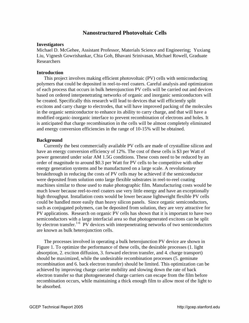
Investigators Michael D. McGehee, Assistant Professor, Materials Science and Engineering; Yuxiang Liu, Vignesh Gowrishankar, Chia Goh, Bhavani Srinivasan, Michael Rowell, Graduate Researchers Introduction This project involves making efficient photovoltaic (PV) cells with semiconducting polymers that could be deposited in reel-to-reel coaters. Careful analysis and optimization of each process that occurs in bulk heterojunction PV cells will be carried out and devices based on ordered interpenetrating networks of organic and inorganic semiconductors will be created. Specifically this research will lead to devices that will efficiently split excitons and carry charge to electrodes, that will have improved packing of the molecules in the organic semiconductor to enhance its ability to carry charge, and that will have a modified organic-inorganic interface to prevent recombination of electrons and holes. It is anticipated that charge recombination in the cells will be almost completely eliminated and energy conversion efficiencies in the range of 10-15% will be obtained. Background Currently the best commercially available PV cells are made of crystalline silicon and have an energy conversion efficiency of 12%. The cost of these cells is $3 per Watt of power generated under solar AM 1.5G conditions. These costs need to be reduced by an order of magnitude to around $0.3 per Watt for PV cells to be competitive with other energy generation systems and be manufactured on a large scale. A revolutionary breakthrough in reducing the costs of PV cells may be achieved if the semiconductor were deposited from solution onto large flexible substrates in reel-to-reel coating machines similar to those used to make photographic film. Manufacturing costs would be much lower because reel-to-reel coaters use very little energy and have an exceptionally high throughput. Installation costs would be lower because lightweight flexible PV cells could be handled more easily than heavy silicon panels. Since organic semiconductors, such as conjugated polymers, can be deposited from solution, they are very attractive for PV applications. Research on organic PV cells has shown that it is important to have two semiconductors with a large interfacial area so that photogenerated excitons can be split by electron transfer.1-6 PV devices with interpenetrating networks of two semiconductors are known as bulk heterojunction cells. The processes involved in operating a bulk heterojunction PV device are shown in Figure 1. To optimize the performance of these cells, the desirable processes (1. light absorption, 2. exciton diffusion, 3. forward electron transfer, and 4. charge transport) should be maximized, while the undesirable recombination processes (5. geminate recombination and 6. back electron transfer) should be limited. This optimization can be achieved by improving charge carrier mobility and slowing down the rate of back electron transfer so that photogenerated charge carriers can escape from the film before recombination occurs, while maintaining a thick enough film to allow most of the light to be absorbed.
Figure 1: A schematic diagram of the energy levels in an organic heterojunction photovoltaic cell and the electronic processes (defined in the text) that occur in one.
Results Since the project began in January of 2004, we have focused our research on making inorganic semiconductor films with straight pores, improving exciton transport to organic-inorganic interfaces, optimizing the organic-inorganic interface and increasing the charge carrier mobility of conjugated polymers confined to nanopores. These are important steps towards our long-term goal of enabling the reel-to-reel manufacturing of bulk heterojunction PV cells.
Fabrication of nanoporous semiconductor films Before the GCEP project began, we showed that films of titania with a semiordered array of connected 8-nm-diameter ellipsoidal pores can be self-assembled by dip coating substrates with a mixture of a block copolymer and titanium ethoxide and then heating the film to remove the block copolymer.7,8 We found that the films could be filled with the semiconducting polymer regioregular poly(3-hexyl thiophene) (P3HT) and that PV cells could be made, but that the efficiency was poor because the P3HT chains were stuck in a non-optimal coiled conformation in the small pores, which causes the charge carrier mobility to be low. We hypothesized that charge transport could be improved if the pores were slightly larger and straighter. To see if simply increasing the pore size would help, we used a structure directing block copolymer with a higher molecular weight than the one we had used previously. The pore size was increased to 20 nm, but we saw no improvement in device efficiency. Analysis of the absorption and photoluminescence spectra of the polymers indicated that the polymers chains were still coiled in the pores, which is not surprising since the pore walls are highly curved. For this reason, we have focused on making straight pores over the last year.
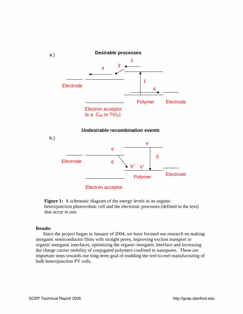
We have fabricated densely-spaced, well-ordered arrays of nanopillars in Si, which could be used as the inorganic semiconductor-phase in bulk-heterojunction PV cells. The nanopillars cover a large area (of the order of sq. cm.), occur with periodicities of ~35 nm, are taller than 100 nm and have aspect-ratios as high as 10 (Figure 2). Block copolymer lithography (using poly(styrene-b-methylmethacrylate)) was used to form the template for patterning the silicon substrate via metal deposition and liftoff. The need to fabricate high-aspect-ratio nanopillars necessitates the use of a highly selective, anisotropic etch chemistry or a sufficiently thick etch mask or both. However, block copolymer lithography does not allow for thick etch masks (thicker than 5 – 10 nm) to be deposited because of prohibitive problems in the liftoff step. Furthermore, even with a very thin layer of the etch mask (under 5 nm), liftoff is not trivial and only seems to occur in sporadic domains a few microns across, at most. We have used a novel way to circumvent the liftoff problem as well as an uncommon Reactive-Ion-Etch (RIE) chemistry to achieve the nanostructures. Preliminary results of silicon-polymer solar cells show promise. Infiltrating the polymer semiconductor into the silicon nanostructure would enable us to fabricate ordered, bulk-heterojunction solar cells. We are writing up a more detailed description of this research for publication and can provide a manuscript to the GCEP sponsors in June 2005.
Figure 2: 90-nm-tall pillars in Si spaced by about 15 nm. These pillars were obtained using block copolymer lithography and reactive ion etching.
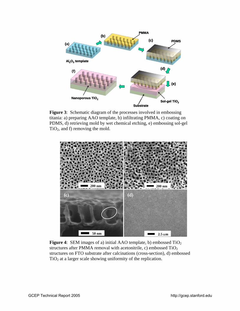
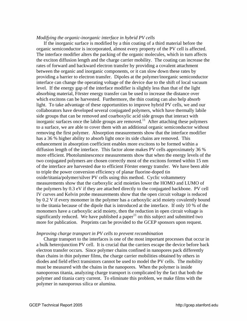
The second approach we have developed to make straight pores is to use anodic alumina to make polymer molds, which can be used to emboss titania sol-gel precursors.9 Anodic alumina has a honeycomb structure with pores in the 10 –1000 nm diameter range. It would be perfect itself for bulk heterojunction PV cells if alumina were a semiconductor. If polydimethysilizane or other elastomers are used as mold materials, the features in the mold stick to each other when removed from the anodic alumina.10 For this reason, we typically fill the anodic alumina with low molecular weight poly(methyl methacrylate), which is a relatively stiff polymer. After we etch away the alumina, we are left with a hard mold of patterned poly(methyl methacrylate). We then press this into a wet film of titania ethoxide that is only partially hydrolyzed and condensed. At this point we heat the film to condense the titania. We then dissolve away the polymer. Figures 3 and 4 show a schematic of the process we used and micrographs of the anodic alumina, mold and embossed titania. We have submitted a more detailed description of this research for publication and can provide a preprint to the GCEP sponsors upon request.
Figure 3: Schematic diagram of the processes involved in embossing titania: a) preparing AAO template, b) infiltrating PMMA, c) coating on PDMS, d) retrieving mold by wet chemical etching, e) embossing sol-gel TiO2, and f) removing the mold.
Figure 4: SEM images of a) initial AAO template, b) embossed TiO2 structures after PMMA removal with acetonitrile, c) embossed TiO2 structures on FTO substrate after calcinations (cross-section), d) embossed TiO2 at a larger scale showing uniformity of the replication.
Modifying the organic-inorganic interface in hybrid PV cells If the inorganic surface is modified by a thin coating of a third material before the organic semiconductor is incorporated, almost every property of the PV cell is affected. The interface modifier alters the packing of the organic molecules, which in turn affects the exciton diffusion length and the charge carrier mobility. The coating can increase the rates of forward and backward electron transfer by providing a covalent attachment between the organic and inorganic components, or it can slow down these rates by providing a barrier to electron transfer. Dipoles at the polymer/inorganic semiconductor interface can change the operating voltage of the device due to the shift of local vacuum level. If the energy gap of the interface modifier is slightly less than that of the light absorbing material, Förster energy transfer can be used to increase the distance over which excitons can be harvested. Furthermore, the thin coating can also help absorb light. To take advantage of these opportunities to improve hybrid PV cells, we and our collaborators have developed several conjugated polymers, which have thermally labile side groups that can be removed and coarboxylic acid side groups that interact with inorganic surfaces once the labile groups are removed.11 After attaching these polymers to a surface, we are able to cover them with an additional organic semiconductor without removing the first polymer. Absorption measurements show that the interface modifier has a 36 % higher ability to absorb light once its side chains are removed. This enhancement in absorption coefficient enables more excitons to be formed within a diffusion length of the interface. This factor alone makes PV cells approximately 36 % more efficient. Photoluminescence measurements show that when the energy levels of the two conjugated polymers are chosen correctly most of the excitons formed within 15 nm of the interface are harvested due to efficient Förster energy transfer. We have been able to triple the power conversion efficiency of planar fluorine-doped tin oxide/titania/polymer/silver PV cells using this method. Cyclic voltammetry measurements show that the carboxylic acid moieties lower the HOMO and LUMO of the polymers by 0.3 eV if they are attached directly to the conjugated backbone. PV cell IV curves and Kelvin probe measurements show that the open circuit voltage is reduced by 0.2 V if every monomer in the polymer has a carboxylic acid moiety covalently bound to the titania because of the dipole that is introduced at the interface. If only 10 % of the monomers have a carboxylic acid moiety, then the reduction in open circuit voltage is significantly reduced. We have published a paper11 on this subject and submitted two more for publication. Preprints can be provided to the GCEP sponsors upon request. Improving charge transport in PV cells to prevent recombination
Charge transport to the interfaces is one of the most important processes that occur in a bulk heterojunction PV cell. It is crucial that the carriers escape the device before back electron transfer occurs. Since polymer chains confined in nanopores pack differently than chains in thin polymer films, the charge carrier mobilities obtained by others in diodes and field effect transistors cannot be used to model the PV cells. The mobility must be measured with the chains in the nanopores. When the polymer is inside nanoporous titania, analyzing charge transport is complicated by the fact that both the polymer and titania carry current. To eliminate this problem, we make films with the polymer in nanoporous silica or alumina.
When we make diodes with poly (3-hexyl thiophene) (P3HT) in nanoporous silica, which has a pore structure identical to the nanoporous titania we self assemble with block copolymers, we find that the current-voltage curves can be fit to a space charge limited current model.12 The mobility is on the order of 10-9 cm2/Vs, which is extremely low. For comparison, the mobility measured in diodes of just the polymer is 10-4 cm2/Vs, and the mobility in field effect transistors (FETs) made with the polymer is 10-1 cm2/Vs.[13] The FET mobility is higher than the diode mobility because the chains lie in the plane of the film and FETs have charge transport in the film while diodes have transport perpendicular to the film. We attribute the extremely low mobility in the mesoporous silica to the highly coiled polymer conformation that is induced by the curved pore walls.
We have formed films of anodic alumina with arrays of straight nanopores on indium
tin oxide (ITO) electrodes. We filled the pores with conjugated polymers, including P3HT and OC1C10-PPV, by spin casting the polymers over the pores and then melting the film. Scanning electron microscopy, photoabsorption spectroscopy and depth profiling confirm that the polymer fills the pores. Measurements of the transmission and reflectance of s and p-polarized light as a function of angle, show that the polymer in the nanopores is partially aligned in the direction perpendicular to the substrate as compared to a neat film. We thermally evaporated high work function electrodes on top of the polymer to make hole-only diodes, which can be used to measure the mobility in the direction perpendicular to the substrate by fitting the I-V characteristics to a space charge limited current (SCLC) model. In the case of P3HT, which is known to have anisotropic transport characteristics, we see a substantial (> 50x) enhancement in current as compared to neat films of equivalently thick polymer. We have simulated the electrodynamics in the semiconductor (polymer) – insulator (alumina) nanostructure using the device simulation program Medici to account for a possible increase in current due to the dielectric environment in the nanopores. It was found that a correction factor between two and four was needed, depending on pore diameter and thickness. Including this correction, we obtained a mobility of greater than 0.006 cm2/Vs which is a factor of 20 higher than the highest diode mobility seen in neat films of P3HT. We believe a mobility as high as 0.1 cm2/Vs can be achieved if the chains are fully aligned since this value has been observed in field effect transistors where the chains lie in the plane of the film and current goes in the plane of the film. In the case of OC1C10-PPV, which is known to have isotropic charge transport characteristics, there was no enhancement in mobility in the anodic alumina-infiltrated polymer diodes. We are currently characterizing other polymers, polymers with varying molecular weight, the effect of treating the surface of the alumina pores before polymer infiltration, and different annealing conditions to further optimize the mobility. These results have important implications for bulk heterojunction photovoltaic cells, which are mainly limited by hole mobility in the polymer. Increased hole mobility in the diode geometry can enable photogenerated carriers to reach the top electrode before recombination with electrons occurs. By replacing the insulating alumina with a semiconductor, such as titania, we should be able to make efficient ordered bulk heterojunction solar cells. A more detailed description of this work has been submitted for publication. A preprint can be provided to the GCEP sponsors upon request.
Progress and Future Plans We are now able to make arrays of silicon nanowires and are exploring the possibility of making silicon-polymer hybrid PV cells. We are also able to emboss a titania precursor paste to make 200-nm thick films of nanoporous titania with 75 nanometer diameter pores. We have made solar cells with these titania films by filling the pores with polymer, but found, not surprisingly, that the excitons could not reach the organic-interface to be split. We are trying to solve this problem by making smaller pores and increasing the diffusion length of excitons in polymers. We have shown that modifying the organic-inorganic interface with a small band gap material has several beneficial effects. The most notable one is that excitons can be transferred to the interface from relatively large distances by Förster energy transfer. We are searching for better combinations of materials so that more of the solar spectrum can be harvested. We have shown that polymer chains can be aligned in 75-nm-diameter pores and that this increases the charge carrier mobility by a factor of 25. We have not been able to achieve suitable charge carrier mobility in smaller pores. We will use x-ray diffraction and spectroscopic measurements to figure out how the molecules pack and why the mobility is lower in the smaller pores. We hope to modify the pore walls and polymer chain length to achieve better chain packing. Our improved ability to fabricate organic-inorganic hybrid nanostructures and understanding of the electronic processes that occur in these films should enable us to make highly efficient photovoltaic cells over the coming two years. Conference Presentations 1. “Fundamental Electronic Processes in Polymeric Photovoltaic Cells” M.D. McGehee,
American Physical Society March Meeting, Los Angeles, CA, March 21-25, 2005. 2. “Improving Exciton and Charge Transport in Organic-Inorganic Hybrid Photovoltaic
Cells,” American Chemical Society, San Diego, CA, March 14-18, 2005. 3. “Tuning the Nanostructure of Semiconducting Polymers to Make Better Photovoltaic
Cells and Transistors” M.D. McGehee, Symposium on Polymer and Molecular Electronics Devices, Singapore, January 10-11, 2005.
4. “The Role of Organic-Inorganic Interfaces in Polymer Field Effect Transistors and Photovoltaic Cells,” M.D. McGehee, K.M. Coakley, Y. Liu, C. Goh, Gordon Conference on Chemistry at Interfaces, New Hampshire, August 15-20, 2004.
5. “Optimizing the Nanostructure of Organic-Inorganic Hybrid Photovoltaic cells” M.D. McGehee, K.M. Coakley, Y. Liu, C. Goh, SPIE’s 49th Annual Meeting, Denver, CO, August 2-6, 2004.
6. “Improving the Interface in Organic-Inorganic Hybrid Photovoltaic Cells,” Y. Liu, S. Scully, N. Dallas, M.D. McGehee, C. Edder, J. Liu, J. Frechet, Spring Materials Research Society Meeting, San Francisco, CA, March 28-April 1, 2005.
7. “Improving Charge Carrier Mobility of Conjugated Polymers by Chain Alignment in Nanopores,” B. Srinivasan, K.M. Coakley, C. Goh, Y. Liu, M.D. McGehee, Spring Materials Research Society Meeting, San Francisco, CA, March 28-April 1, 2005.
8. “Aligning Conjugated Polymers in Nanopores to Improve Bulk Heterojunction Photovoltaic Cells,” C. Goh, K.M. Coakley, Y. Liu, M.D. McGehee, Fall Materials Research Society Meeting, Boston, MA, November 29 – December 3, 2004.
9. “Ordered Nanostructures for Organic Photovoltaic Cells,” Gowrishankar, V, M.D. McGehee, Materials Research Society Fall Meeting, Boston, MA, November 29 - Dec 3, 2004.
3. “Polythiophene containing thermally removable solubilizing groups enhances the interface and the performance of polymer-titania hybrid solar cells” J.S. Liu, E.N. Kadnikova, Y. Liu, M.D. McGehee, J.M.J. Frechet, Journal of the American Chemical Society, 126 (2004) 9486-7.
Several manuscripts have been submitted and should be published by the end of 2005. References (1) Yu, G.; Gao, J.; Hummelen, J. C.; Wudl, F.; Heeger, A. J. Science 1995, 270,
1789-91. (2) Shaheen, S. E.; Brabec, C. J.; Sariciftci, N. S.; Padinger, F.; Fromherz, T.;
Hummelen, J. C. Appl. Phys. Lett. 2001, 78, 841-843. (3) Huynh, W. U.; Dittmer, J. J.; Alivisatos, A. P. Science 2002, 295, 2425-2427. (4) Peumans, P.; Yakimov, A.; Forrest, S. J. of Appl. Phys. 2003, 93, 3693-3723. (5) Shaheen, S. E.; Ginley, D. S.; Jabbour, G. E. MRS Bulletin 2005, 30, 10-15. (6) Coakley, K. M.; McGehee, M. D. Chem. Mater. 2004, 16, 4533-4542. (7) Coakley, K. M.; Y., L.; McGehee, M. D.; Frindell, K. M.; Stucky, G. D. Adv.
Funct. Mater. 2003, 13, 301-306. (8) Coakley, K. M.; McGehee, M. D. Appl. Phys. Lett. 2003, 83, 3380-2. (9) Masuda, H.; Nishio, K.; Baba, N. Jpn. J. Appl. Phys. 1992, 31, L 1775- L 1777. (10) Odom, T.; Love, C.; Wolfe, D.; Paul, K.; Whitesides, G. Langmuir 2002, 18,
5314-5320. (11) Liu, J.; Kadnikova, E. N.; Liu, Y.; McGehee, M. D.; Frechet, J. M. J. J. Am.
Chem. Soc. 2004, 126, 9486-7. (12) Bozano, L.; Carter, S. A.; Scott, J. C.; Malliaras, G. G.; Brock, P. J. Appl. Phys.