23 May 2006 LCFI Collab Meeting – Chris Damerell 1 Low-capacitance CCD Chris Damerell An idea to reduce inter-gate capacitance in CPCCDs, hoping to achieve busline distribution of clocks and hence minimal demands on driver and storage capacitors Valuable help and advice from Konstantin, Brian Hawes, Rainer Richter (MPI) and David Burt – and all who came to the e2V meeting on 18 th May Started as a cross-check whether the DALSA inter-gate figure of 0.33 pF/cm (per edge) was at all credible, contrary to simulations by Konstantin and Brian and opinions at e2V …
Transcript
23 May 2006 LCFI Collab Meeting – Chris Damerell1
Low-capacitance CCD
Chris Damerell
An idea to reduce inter-gate capacitance in CPCCDs, hoping to achieve
busline distribution of clocks and hence minimal demands on driver and storage capacitors
Valuable help and advice from Konstantin, Brian Hawes, Rainer Richter (MPI) and David Burt – and all who came to the e2V meeting on 18th May
Started as a cross-check whether the DALSA inter-gate figure of 0.33 pF/cm (per edge) was at all credible, contrary to simulations by Konstantin and Brian and opinions at e2V …
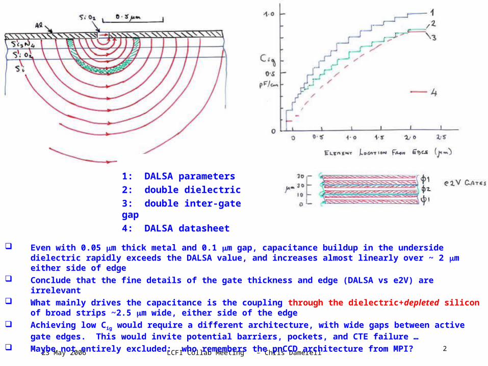
23 May 2006 LCFI Collab Meeting – Chris Damerell2
Even with 0.05 m thick metal and 0.1 m gap, capacitance buildup in the underside dielectric
rapidly exceeds the DALSA value, and increases almost linearly over ~ 2 m either side of edge Conclude that the fine details of the gate thickness and edge (DALSA vs e2V) are irrelevant What mainly drives the capacitance is the coupling through the dielectric+depleted silicon of broad
strips ~2.5 m wide, either side of the edge Achieving low Cig would require a different architecture, with wide gaps between active gate edges.
This would invite potential barriers, pockets, and CTE failure … Maybe not entirely excluded: who remembers the pnCCD architecture from MPI?
1: DALSA parameters
2: double dielectric
3: double inter-gate gap
4: DALSA datasheet
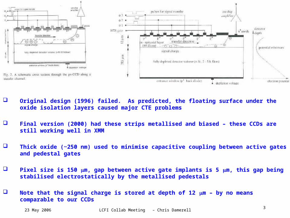
23 May 2006 LCFI Collab Meeting – Chris Damerell3
Original design (1996) failed. As predicted, the floating surface under the oxide isolation layers
caused major CTE problems
Final version (2000) had these strips metallised and biased – these CCDs are still working well in XMM
Thick oxide (~250 nm) used to minimise capacitive coupling between active gates and pedestal gates
Pixel size is 150 m, gap between active gate implants is 5 m, this gap being stabilised electrostatically by the metallised pedestals
Note that the signal charge is stored at depth of 12 m – by no means comparable to our CCDs
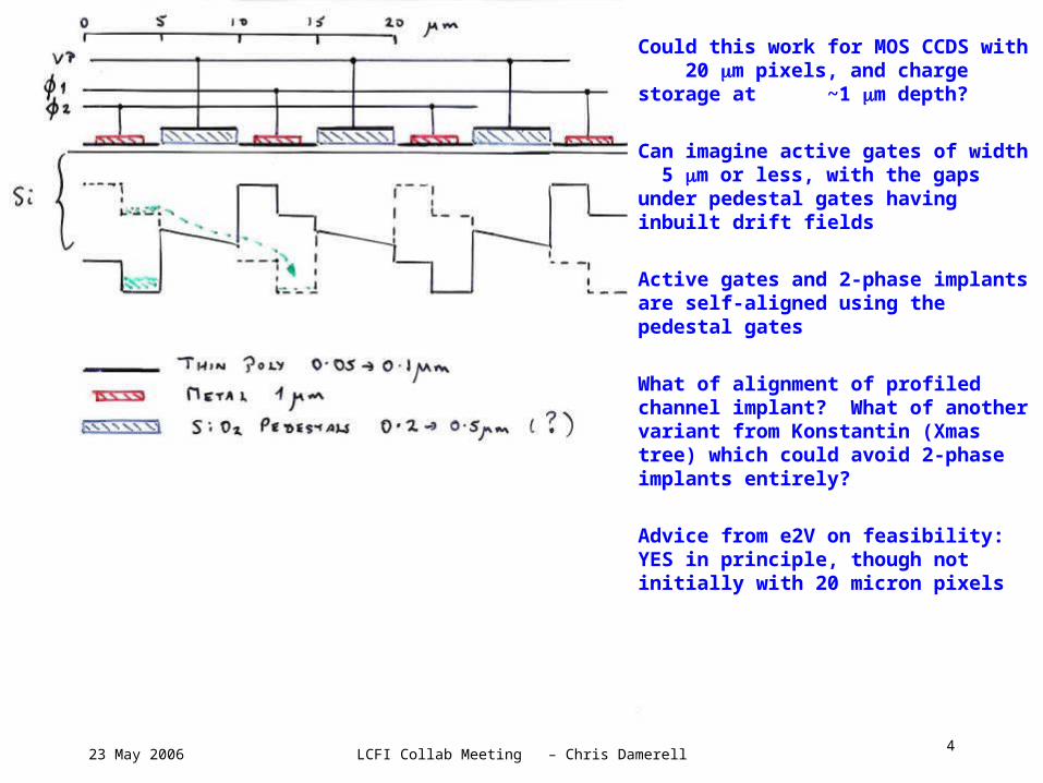
23 May 2006 LCFI Collab Meeting – Chris Damerell4
Could this work for MOS CCDS with 20 m pixels, and charge storage at ~1 m depth?
Can imagine active gates of width 5 m or less, with the gaps under pedestal gates having inbuilt drift fields
Active gates and 2-phase implants are self-aligned using the pedestal gates
What of alignment of profiled channel implant? What of another variant from Konstantin (Xmas tree) which could avoid 2-phase implants entirely?
Advice from e2V on feasibility: YES in principle, though not initially with 20 micron pixels
23 May 2006 LCFI Collab Meeting – Chris Damerell5
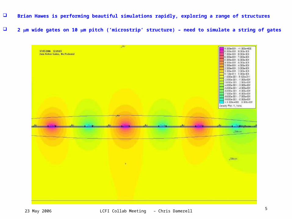
Brian Hawes is performing beautiful simulations rapidly, exploring a range of structures
2 m wide gates on 10 m pitch (’microstrip’ structure) – need to simulate a string of gates
23 May 2006 LCFI Collab Meeting – Chris Damerell6
Rough approximation to e2V gates – 10 m pitch and 0.1 m gaps
Can ‘see’ the field lines, but it will be nice if possible to have a computer-generated one, lines spaced at equal intervals of surface charge
2 m wide gates on 10 m pitch (’microstrip’ structure) – need to simulate a string of gates
23 May 2006 LCFI Collab Meeting – Chris Damerell7
Parameters in this example:
• active gate length = pedestal gate length = 5 m• gate thickness (active and pedestal) = 0.1 m• Pedestal height = 0.5 m oxide• Dielectric isolation above Si: 85 nm oxide plus 85 nm nitride (e2V standard)
23 May 2006 LCFI Collab Meeting – Chris Damerell8
For min cap in open phase region, actually better to fill the available space with pedestal gate,
completely avoiding any implanted region• 8 m wide pedestal, Ceff = 1.98 pF/cm if 0.5 m high, 2.61 pF/cm if 0.2 m high
• 3/2/3 m wide implant/pedestal/implant shown above gives 3.06 pF/cm if 0.2 m high • All implant (not feasible in practice) gives 3.09 pF/cm
23 May 2006 LCFI Collab Meeting – Chris Damerell9
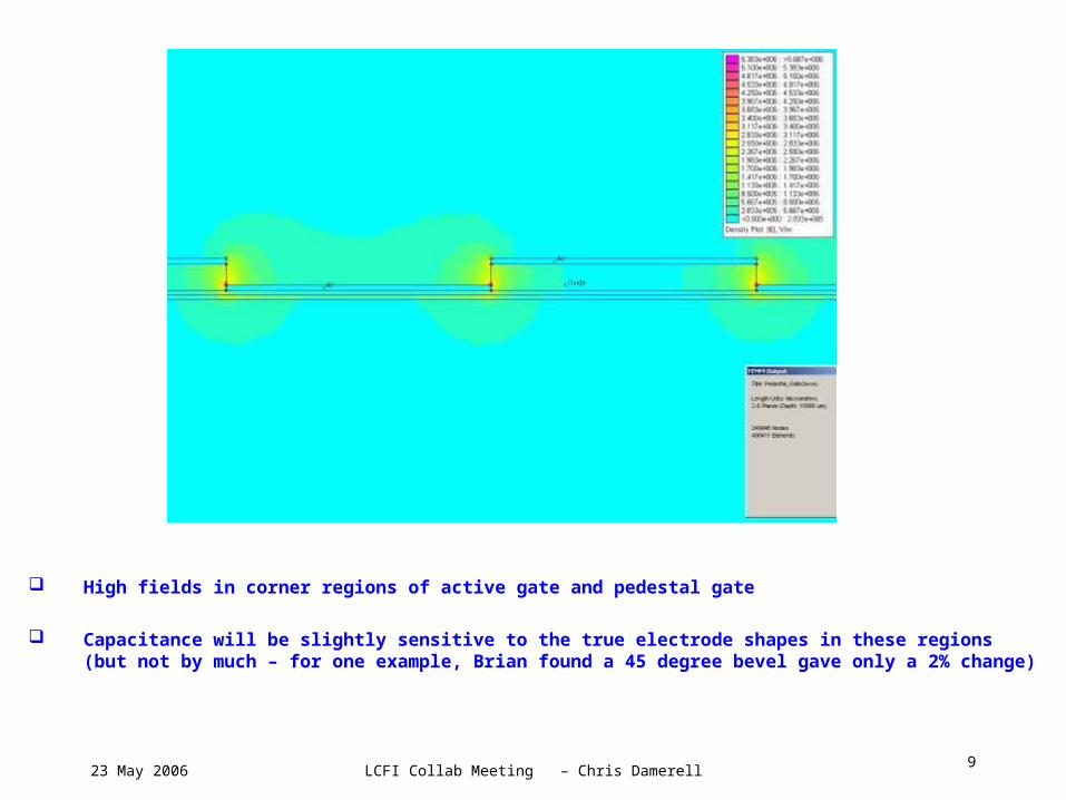
High fields in corner regions of active gate and pedestal gate
Capacitance will be slightly sensitive to the true electrode shapes in these regions (but not by much – for one example, Brian found a 45 degree bevel gave only a 2% change)
23 May 2006 LCFI Collab Meeting – Chris Damerell10
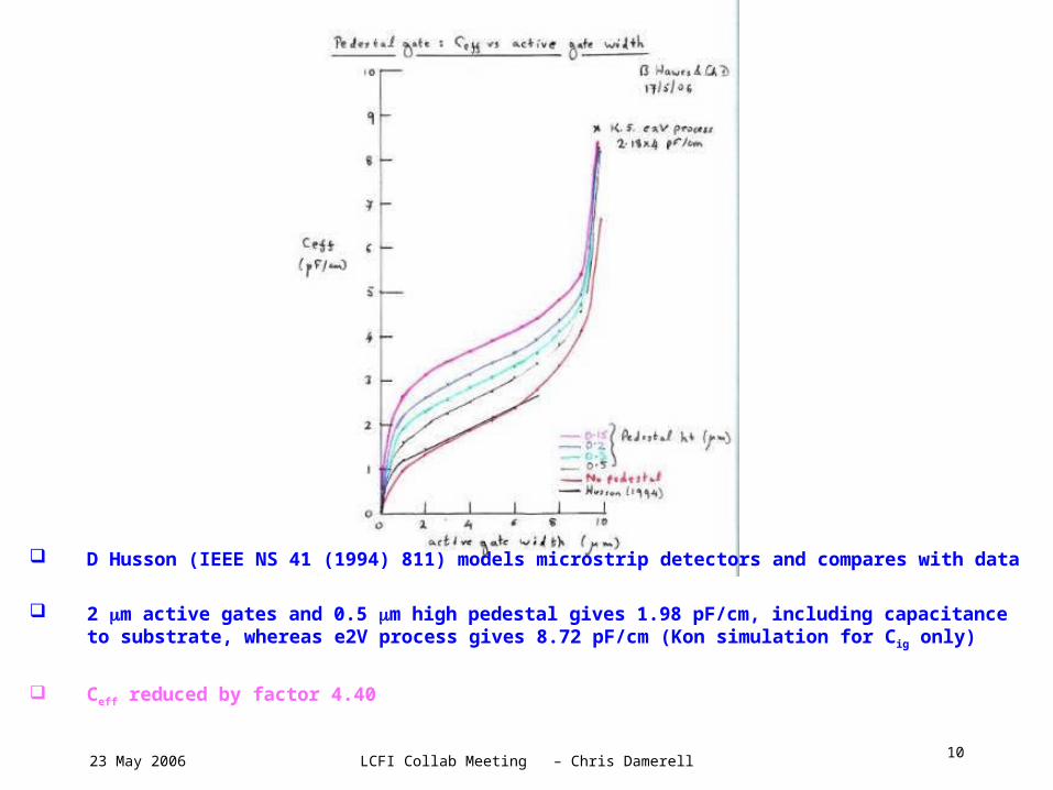
D Husson (IEEE NS 41 (1994) 811) models microstrip detectors and compares with data
2 m active gates and 0.5 m high pedestal gives 1.98 pF/cm, including capacitance to substrate, whereas e2V process gives 8.72 pF/cm (Kon simulation for C ig only)
Ceff reduced by factor 4.40
23 May 2006 LCFI Collab Meeting – Chris Damerell11
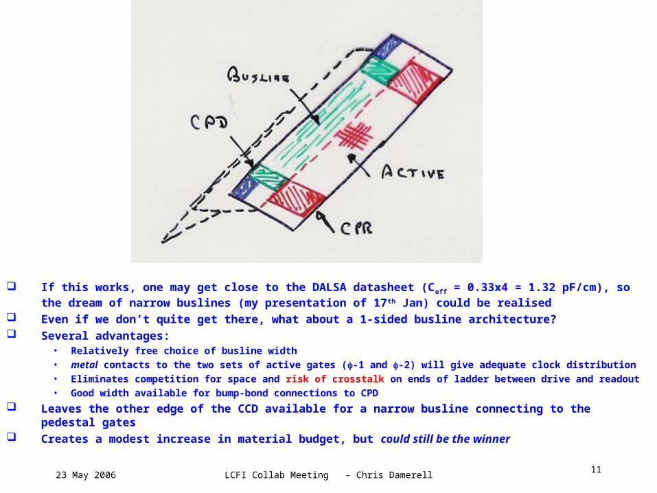
If this works, one may get close to the DALSA datasheet (Ceff = 0.33x4 = 1.32 pF/cm), so the dream
of narrow buslines (my presentation of 17th Jan) could be realised Even if we don’t quite get there, what about a 1-sided busline architecture? Several advantages:
• Relatively free choice of busline width• metal contacts to the two sets of active gates (-1 and -2) will give adequate clock distribution• Eliminates competition for space and risk of crosstalk on ends of ladder between drive and readout• Good width available for bump-bond connections to CPD
Leaves the other edge of the CCD available for a narrow busline connecting to the pedestal gates Creates a modest increase in material budget, but could still be the winner
23 May 2006 LCFI Collab Meeting – Chris Damerell12
There are several possible showstoppers, even if such a structure can be made:
• Potential barriers or pockets at the transitions between active gates and pedestal gates
• Jitter in potential under the pedestal gate, due to fluctuations in phi-1 and phi-2 waveforms
• Radiation-induced shifts in this potential. However, if this is uniform across the device, it can be eliminated by adjusting the pedestal gate voltage
The possibility of greatly reduced CCD capacitance is of general interest. It has always been frustrating that transferring such small signal charges needed such high driver power
If it can be made to work, there could be wider applications
We have started to discuss possible test structures with e2V
We (Brian?) could extend the model outwards from the CCD, back through the buslines (how wide should they really be?) and through bump bonds back to the CPD output